EP1761117A1 - Wiring board with embedded ceramic capacitors - Google Patents
Wiring board with embedded ceramic capacitors Download PDFInfo
- Publication number
- EP1761117A1 EP1761117A1 EP06018327A EP06018327A EP1761117A1 EP 1761117 A1 EP1761117 A1 EP 1761117A1 EP 06018327 A EP06018327 A EP 06018327A EP 06018327 A EP06018327 A EP 06018327A EP 1761117 A1 EP1761117 A1 EP 1761117A1
- Authority
- EP
- European Patent Office
- Prior art keywords
- layer
- main surface
- core
- capacitor
- wiring board
- Prior art date
- Legal status (The legal status is an assumption and is not a legal conclusion. Google has not performed a legal analysis and makes no representation as to the accuracy of the status listed.)
- Withdrawn
Links
Images




Classifications
-
- H—ELECTRICITY
- H05—ELECTRIC TECHNIQUES NOT OTHERWISE PROVIDED FOR
- H05K—PRINTED CIRCUITS; CASINGS OR CONSTRUCTIONAL DETAILS OF ELECTRIC APPARATUS; MANUFACTURE OF ASSEMBLAGES OF ELECTRICAL COMPONENTS
- H05K1/00—Printed circuits
- H05K1/18—Printed circuits structurally associated with non-printed electric components
- H05K1/182—Printed circuits structurally associated with non-printed electric components associated with components mounted in printed circuit boards [PCB], e.g. insert-mounted components [IMC]
- H05K1/185—Printed circuits structurally associated with non-printed electric components associated with components mounted in printed circuit boards [PCB], e.g. insert-mounted components [IMC] associated with components encapsulated in the insulating substrate of the PCBs; associated with components incorporated in internal layers of multilayer circuit boards
-
- H—ELECTRICITY
- H01—ELECTRIC ELEMENTS
- H01G—CAPACITORS; CAPACITORS, RECTIFIERS, DETECTORS, SWITCHING DEVICES, LIGHT-SENSITIVE OR TEMPERATURE-SENSITIVE DEVICES OF THE ELECTROLYTIC TYPE
- H01G2/00—Details of capacitors not covered by a single one of groups H01G4/00-H01G11/00
- H01G2/02—Mountings
- H01G2/06—Mountings specially adapted for mounting on a printed-circuit support
-
- H—ELECTRICITY
- H01—ELECTRIC ELEMENTS
- H01G—CAPACITORS; CAPACITORS, RECTIFIERS, DETECTORS, SWITCHING DEVICES, LIGHT-SENSITIVE OR TEMPERATURE-SENSITIVE DEVICES OF THE ELECTROLYTIC TYPE
- H01G4/00—Fixed capacitors; Processes of their manufacture
- H01G4/38—Multiple capacitors, i.e. structural combinations of fixed capacitors
-
- H—ELECTRICITY
- H05—ELECTRIC TECHNIQUES NOT OTHERWISE PROVIDED FOR
- H05K—PRINTED CIRCUITS; CASINGS OR CONSTRUCTIONAL DETAILS OF ELECTRIC APPARATUS; MANUFACTURE OF ASSEMBLAGES OF ELECTRICAL COMPONENTS
- H05K1/00—Printed circuits
- H05K1/02—Details
- H05K1/0213—Electrical arrangements not otherwise provided for
- H05K1/0216—Reduction of cross-talk, noise or electromagnetic interference
- H05K1/023—Reduction of cross-talk, noise or electromagnetic interference using auxiliary mounted passive components or auxiliary substances
- H05K1/0231—Capacitors or dielectric substances
-
- H—ELECTRICITY
- H10—SEMICONDUCTOR DEVICES; ELECTRIC SOLID-STATE DEVICES NOT OTHERWISE PROVIDED FOR
- H10P—GENERIC PROCESSES OR APPARATUS FOR THE MANUFACTURE OR TREATMENT OF DEVICES COVERED BY CLASS H10
- H10P72/00—Handling or holding of wafers, substrates or devices during manufacture or treatment thereof
- H10P72/70—Handling or holding of wafers, substrates or devices during manufacture or treatment thereof for supporting or gripping
- H10P72/74—Handling or holding of wafers, substrates or devices during manufacture or treatment thereof for supporting or gripping using temporarily an auxiliary support
-
- H—ELECTRICITY
- H10—SEMICONDUCTOR DEVICES; ELECTRIC SOLID-STATE DEVICES NOT OTHERWISE PROVIDED FOR
- H10W—GENERIC PACKAGES, INTERCONNECTIONS, CONNECTORS OR OTHER CONSTRUCTIONAL DETAILS OF DEVICES COVERED BY CLASS H10
- H10W44/00—Electrical arrangements for controlling or matching impedance
- H10W44/601—Capacitive arrangements
-
- H—ELECTRICITY
- H10—SEMICONDUCTOR DEVICES; ELECTRIC SOLID-STATE DEVICES NOT OTHERWISE PROVIDED FOR
- H10W—GENERIC PACKAGES, INTERCONNECTIONS, CONNECTORS OR OTHER CONSTRUCTIONAL DETAILS OF DEVICES COVERED BY CLASS H10
- H10W70/00—Package substrates; Interposers; Redistribution layers [RDL]
- H10W70/60—Insulating or insulated package substrates; Interposers; Redistribution layers
- H10W70/611—Insulating or insulated package substrates; Interposers; Redistribution layers for connecting multiple chips together
-
- H—ELECTRICITY
- H10—SEMICONDUCTOR DEVICES; ELECTRIC SOLID-STATE DEVICES NOT OTHERWISE PROVIDED FOR
- H10W—GENERIC PACKAGES, INTERCONNECTIONS, CONNECTORS OR OTHER CONSTRUCTIONAL DETAILS OF DEVICES COVERED BY CLASS H10
- H10W70/00—Package substrates; Interposers; Redistribution layers [RDL]
- H10W70/60—Insulating or insulated package substrates; Interposers; Redistribution layers
- H10W70/67—Insulating or insulated package substrates; Interposers; Redistribution layers characterised by their insulating layers or insulating parts
- H10W70/68—Shapes or dispositions thereof
- H10W70/685—Shapes or dispositions thereof comprising multiple insulating layers
-
- H—ELECTRICITY
- H10—SEMICONDUCTOR DEVICES; ELECTRIC SOLID-STATE DEVICES NOT OTHERWISE PROVIDED FOR
- H10W—GENERIC PACKAGES, INTERCONNECTIONS, CONNECTORS OR OTHER CONSTRUCTIONAL DETAILS OF DEVICES COVERED BY CLASS H10
- H10W72/00—Interconnections or connectors in packages
-
- H—ELECTRICITY
- H10—SEMICONDUCTOR DEVICES; ELECTRIC SOLID-STATE DEVICES NOT OTHERWISE PROVIDED FOR
- H10W—GENERIC PACKAGES, INTERCONNECTIONS, CONNECTORS OR OTHER CONSTRUCTIONAL DETAILS OF DEVICES COVERED BY CLASS H10
- H10W74/00—Encapsulations, e.g. protective coatings
- H10W74/01—Manufacture or treatment
- H10W74/019—Manufacture or treatment using temporary auxiliary substrates
-
- H—ELECTRICITY
- H05—ELECTRIC TECHNIQUES NOT OTHERWISE PROVIDED FOR
- H05K—PRINTED CIRCUITS; CASINGS OR CONSTRUCTIONAL DETAILS OF ELECTRIC APPARATUS; MANUFACTURE OF ASSEMBLAGES OF ELECTRICAL COMPONENTS
- H05K2201/00—Indexing scheme relating to printed circuits covered by H05K1/00
- H05K2201/10—Details of components or other objects attached to or integrated in a printed circuit board
- H05K2201/10431—Details of mounted components
- H05K2201/10507—Involving several components
- H05K2201/10522—Adjacent components
-
- H—ELECTRICITY
- H05—ELECTRIC TECHNIQUES NOT OTHERWISE PROVIDED FOR
- H05K—PRINTED CIRCUITS; CASINGS OR CONSTRUCTIONAL DETAILS OF ELECTRIC APPARATUS; MANUFACTURE OF ASSEMBLAGES OF ELECTRICAL COMPONENTS
- H05K2201/00—Indexing scheme relating to printed circuits covered by H05K1/00
- H05K2201/10—Details of components or other objects attached to or integrated in a printed circuit board
- H05K2201/10613—Details of electrical connections of non-printed components, e.g. special leads
- H05K2201/10621—Components characterised by their electrical contacts
- H05K2201/10674—Flip chip
-
- H—ELECTRICITY
- H05—ELECTRIC TECHNIQUES NOT OTHERWISE PROVIDED FOR
- H05K—PRINTED CIRCUITS; CASINGS OR CONSTRUCTIONAL DETAILS OF ELECTRIC APPARATUS; MANUFACTURE OF ASSEMBLAGES OF ELECTRICAL COMPONENTS
- H05K2201/00—Indexing scheme relating to printed circuits covered by H05K1/00
- H05K2201/10—Details of components or other objects attached to or integrated in a printed circuit board
- H05K2201/10613—Details of electrical connections of non-printed components, e.g. special leads
- H05K2201/10621—Components characterised by their electrical contacts
- H05K2201/10712—Via grid array, e.g. via grid array capacitor
-
- H—ELECTRICITY
- H05—ELECTRIC TECHNIQUES NOT OTHERWISE PROVIDED FOR
- H05K—PRINTED CIRCUITS; CASINGS OR CONSTRUCTIONAL DETAILS OF ELECTRIC APPARATUS; MANUFACTURE OF ASSEMBLAGES OF ELECTRICAL COMPONENTS
- H05K3/00—Apparatus or processes for manufacturing printed circuits
- H05K3/46—Manufacturing multilayer circuits
- H05K3/4602—Manufacturing multilayer circuits characterized by a special circuit board as base or central core whereon additional circuit layers are built or additional circuit boards are laminated
-
- H—ELECTRICITY
- H10—SEMICONDUCTOR DEVICES; ELECTRIC SOLID-STATE DEVICES NOT OTHERWISE PROVIDED FOR
- H10P—GENERIC PROCESSES OR APPARATUS FOR THE MANUFACTURE OR TREATMENT OF DEVICES COVERED BY CLASS H10
- H10P72/00—Handling or holding of wafers, substrates or devices during manufacture or treatment thereof
- H10P72/70—Handling or holding of wafers, substrates or devices during manufacture or treatment thereof for supporting or gripping
- H10P72/74—Handling or holding of wafers, substrates or devices during manufacture or treatment thereof for supporting or gripping using temporarily an auxiliary support
- H10P72/7424—Handling or holding of wafers, substrates or devices during manufacture or treatment thereof for supporting or gripping using temporarily an auxiliary support used as a support during the manufacture of self-supporting substrates
-
- H—ELECTRICITY
- H10—SEMICONDUCTOR DEVICES; ELECTRIC SOLID-STATE DEVICES NOT OTHERWISE PROVIDED FOR
- H10W—GENERIC PACKAGES, INTERCONNECTIONS, CONNECTORS OR OTHER CONSTRUCTIONAL DETAILS OF DEVICES COVERED BY CLASS H10
- H10W70/00—Package substrates; Interposers; Redistribution layers [RDL]
- H10W70/60—Insulating or insulated package substrates; Interposers; Redistribution layers
- H10W70/62—Insulating or insulated package substrates; Interposers; Redistribution layers characterised by their interconnections
- H10W70/65—Shapes or dispositions of interconnections
-
- H—ELECTRICITY
- H10—SEMICONDUCTOR DEVICES; ELECTRIC SOLID-STATE DEVICES NOT OTHERWISE PROVIDED FOR
- H10W—GENERIC PACKAGES, INTERCONNECTIONS, CONNECTORS OR OTHER CONSTRUCTIONAL DETAILS OF DEVICES COVERED BY CLASS H10
- H10W70/00—Package substrates; Interposers; Redistribution layers [RDL]
- H10W70/60—Insulating or insulated package substrates; Interposers; Redistribution layers
- H10W70/62—Insulating or insulated package substrates; Interposers; Redistribution layers characterised by their interconnections
- H10W70/65—Shapes or dispositions of interconnections
- H10W70/654—Top-view layouts
- H10W70/655—Fan-out layouts
-
- H—ELECTRICITY
- H10—SEMICONDUCTOR DEVICES; ELECTRIC SOLID-STATE DEVICES NOT OTHERWISE PROVIDED FOR
- H10W—GENERIC PACKAGES, INTERCONNECTIONS, CONNECTORS OR OTHER CONSTRUCTIONAL DETAILS OF DEVICES COVERED BY CLASS H10
- H10W72/00—Interconnections or connectors in packages
- H10W72/071—Connecting or disconnecting
- H10W72/072—Connecting or disconnecting of bump connectors
-
- H—ELECTRICITY
- H10—SEMICONDUCTOR DEVICES; ELECTRIC SOLID-STATE DEVICES NOT OTHERWISE PROVIDED FOR
- H10W—GENERIC PACKAGES, INTERCONNECTIONS, CONNECTORS OR OTHER CONSTRUCTIONAL DETAILS OF DEVICES COVERED BY CLASS H10
- H10W72/00—Interconnections or connectors in packages
- H10W72/071—Connecting or disconnecting
- H10W72/072—Connecting or disconnecting of bump connectors
- H10W72/07231—Techniques
- H10W72/07236—Soldering or alloying
-
- H—ELECTRICITY
- H10—SEMICONDUCTOR DEVICES; ELECTRIC SOLID-STATE DEVICES NOT OTHERWISE PROVIDED FOR
- H10W—GENERIC PACKAGES, INTERCONNECTIONS, CONNECTORS OR OTHER CONSTRUCTIONAL DETAILS OF DEVICES COVERED BY CLASS H10
- H10W72/00—Interconnections or connectors in packages
- H10W72/20—Bump connectors, e.g. solder bumps or copper pillars; Dummy bumps; Thermal bumps
- H10W72/241—Dispositions, e.g. layouts
-
- H—ELECTRICITY
- H10—SEMICONDUCTOR DEVICES; ELECTRIC SOLID-STATE DEVICES NOT OTHERWISE PROVIDED FOR
- H10W—GENERIC PACKAGES, INTERCONNECTIONS, CONNECTORS OR OTHER CONSTRUCTIONAL DETAILS OF DEVICES COVERED BY CLASS H10
- H10W72/00—Interconnections or connectors in packages
- H10W72/90—Bond pads, in general
-
- H—ELECTRICITY
- H10—SEMICONDUCTOR DEVICES; ELECTRIC SOLID-STATE DEVICES NOT OTHERWISE PROVIDED FOR
- H10W—GENERIC PACKAGES, INTERCONNECTIONS, CONNECTORS OR OTHER CONSTRUCTIONAL DETAILS OF DEVICES COVERED BY CLASS H10
- H10W72/00—Interconnections or connectors in packages
- H10W72/90—Bond pads, in general
- H10W72/941—Dispositions of bond pads
- H10W72/9415—Dispositions of bond pads relative to the surface, e.g. recessed, protruding
-
- H—ELECTRICITY
- H10—SEMICONDUCTOR DEVICES; ELECTRIC SOLID-STATE DEVICES NOT OTHERWISE PROVIDED FOR
- H10W—GENERIC PACKAGES, INTERCONNECTIONS, CONNECTORS OR OTHER CONSTRUCTIONAL DETAILS OF DEVICES COVERED BY CLASS H10
- H10W90/00—Package configurations
- H10W90/701—Package configurations characterised by the relative positions of pads or connectors relative to package parts
- H10W90/721—Package configurations characterised by the relative positions of pads or connectors relative to package parts of bump connectors
- H10W90/724—Package configurations characterised by the relative positions of pads or connectors relative to package parts of bump connectors between a chip and a stacked insulating package substrate, interposer or RDL
Definitions
- the present invention is related to a wiring board having a structure wherein a ceramic capacitor is embedded in a substrate core and a built-up layer is laminated on a surface of the substrate core on which a semiconductor integrated circuit element is mounted.
- the semiconductor integrated circuit element (IC chip) used for CPU in a computer etc. has operated at higher speeds with high functioning features.
- the number of terminals increases and the terminal interval tends to be narrow.
- many terminals are densely formed on the bottom surface of the IC chip in an array form, and such a terminal block is connected to a terminal block at the motherboard side by flip chip connection.
- the connection method generally employed is such that a package constituted by the IC chip, which is mounted on a wiring board for mounting the IC chip, is produced and then mounted on the mother board.
- An example of such wiring boards for mounting the IC chip, which constitutes this type of package includes a wiring board where a ceramic chip is embedded in a core substrate, which is comprised of a polymer material, so as to form a core portion, and a built-up layer is formed on both top and rear surfaces of the core portion, respectively (e.g., see Japanese Patent Application Laid-Open (kokai) No. 2005-39243 ).
- One of the examples for such system includes a package having a plurality of microprocessors. That is, this type of package having such multi-microprocessor structure is capable of performing a parallel processing of plural threads (tasks), which a single microprocessor structure or the like cannot perform, resulting in improving the processing capacity of the entire system. Further, a failure-resistance of the multi-microprocessor structure is improved compared to the single microprocessor structure.
- aceramic capacitor in a wiring board according to Japanese Patent Application Laid-Open (kokai) No. 2005-39243 is enlarged, and a microprocessor is mounted on plural locations, respectively, within an accommodation area of the enlarged ceramic capacitor.
- this structure when this structure is adopted, an area in a substrate core for forming a conductor portion, such as a through-hole and a conductive pattern, will decrease.
- a wiring for the conductor portion for used in electrically connecting the top and rear surfaces of a core portion becomes difficult, thereby being unlikely to reduce in the overall size of the wiring board.
- the wiring board according to Japanese Patent Application Laid-Open (kokai) No.2005-39243 canbeusedasacomponent part of a package having the multi-microprocessor structure when a plurality of power supply systems of the microprocessors can be shared.
- the power supply system cannot be shared, and it is necessary to establish the power supply system for every microprocessor, each microprocessor can not be fully operated, even though the wiring board is used as a component part. Therefore, the advantages of multi-microprocessor structure cannot be fully realized.
- the present invention has been accomplished in view of the above problems, and an object of the invention is to provide a wiring board capable of bringing out the advantages of the structure where a plurality of semiconductor integrated circuit elements are mounted, and the wiring board which allows a reduction in size thereof and offers excellent cost performance and reliability.
- the present invention provides the wiring board according to independent claim 1.
- a means for solving the above-mentioned problem is a wiring board, comprising: a substrate core including a core main surface and a core rear surface; a plurality of ceramic capacitors having a capacitor main sur face and a structure where a first inner electrode layer and a second inner electrode layer are alternately laminated by sandwiching a ceramic dielectric layer, wherein said ceramic capacitor is embedded in said substrate core in the state where said core main surface and said capacitor main surface are turned to the same side; and a built-up layer having a structure where an inter layer insulating layer and a conductor layer are alternately laminated on said core main surface and said capacitor main surface, and including a plurality of semiconductor integrated circuit element mounting areas in various locations on a surface of said built-up layer, and wherein said plural ceramic capacitors are disposed in areas of said substrate core, which correspond to said plural semiconductor integrated circuit element mounting areas.
- a plurality of semiconductor integrated circuit element mounting areas on which a semiconductor integrated circuit element may be mounted is provided in the built-uplayer, and, in the substrate core, a plurality of ceramic capacitors are disposed in the areas corresponding to a plurality of semiconductor integrated circuit element mounting areas, respectively. Therefore, a conductor portion, such as a through-hole conductor or a conductor pattern or the like can be formed in an area formed between the adjoining ceramic capacitors.
- a conductor layer can be formed for establishing an electrical connection between the top and rear surfaces of the substrate core, resulting in a prevention of an enlargement of the overall size of the wiring board.
- each semiconductor integrated circuit element can fully operate because the plural ceramic capacitors are electrically connected to the semiconductor integrated circuit element mounting areas, respectively. Therefore, when adopting the structure of mounting a plurality of semiconductor integrated circuit elements, the advantages of such a structure can be fully realized.
- each semiconductor integrated circuit element is supported on each ceramic capacitor.
- the influence of heat stress is reduced because a thermal expansion coefficient with the semiconductor integrated circuit element can easily match. Therefore, a crack and a faulty connection of the semiconductor integrated circuit element due to great heat stress can be prevented.
- each ceramic capacitor is disposed, respectively, in the inner area of the substrate core which is situated generally directly below the plural semiconductor integrated circuit element mounting area.
- Each ceramic capacitor disposed in this way is provided so that a part of or the entire ceramic capacitor may overlap the semiconductor integrated circuit element mounting area, when looking from the thickness direction of the capacitor.
- correlation in the magnitude between the dimension of each ceramic capacitor when looking from the thickness direction of the capacitor and the dimension of each semiconductor integrated circuit element mounting area can be at one's discretion. However, it is preferable that the former dimension be equal to or lager than the latter dimension.
- semiconductor integrated circuit element in the present invention means mainly a semiconductor integrated circuit element used as a microprocessor or the like of a computer.
- the semiconductor integrated circuit element is, for example, flip chip connected to the semiconductor integrated circuit element mounting area.
- semiconductor integrated circuit element mounting area means an area where a terminal pad block is disposed on the surface of the built-up layer. Two or more semiconductor integrated circuit elements mounting areas (i.e., the number of semiconductor integrated circuit element) may be provided.
- the substrate core constituting the above-mentioned wiring board is a part of the core portion in the wiring board, and assumes, for example, a plate-like form or shape having the core main surface and the core rear surface located opposed to the core main surface.
- the substrate core may include one ormore housing opening portion (s) for accommodating the ceramic capacitor.
- the housing opening portion may be a non-through-hole which only opens at the core main surface, or may be a through-hole which opens at both core main surface and core rear surface.
- a preferable substrate core is comprised mainly of a polymer material.
- the polymer materials for forming the substrate core include EP resin (epoxyresin), PI resin (polyimide resin), BT resin (bismaleimide triazine resin), PPE resin (polyphenylene ether resin), etc.
- a composite material made of these resins and organic fibers, such as glass fiber (glass woven fabric and non-woven glass fabric) or polyamide fiber may be employed.
- the ceramic capacitor constituting the above-mentioned wiring board has the capacitor main surface and a structure where the first inner electrode layer and the second inner electrode layer are alternately laminated by sandwiching the ceramic dielectric layer.
- the ceramic capacitor includes a capacitor main surface and a capacitor rear surface, which is located opposite side of the capacitor main surface.
- the ceramic capacitor in the present invention includes a capacitor formed in such a manner that a thin film layer made of ceramic material is laminated on a substrate (not limited to ceramic substrate). The ceramic capacitor is embedded in the substrate core in the state where the core main surface and the capacitor main surface are turned to the same side.
- embedded here means the state where at least a part of a ceramic capacitor is accommodated in the housing opening portion of the substrate core or the state where the entire ceramic capacitor is accommodated in the housing opening portion of the substrate core. Further, the ceramic capacitor is fixed by a filler made from, for example, a polymer material in the state that the ceramic capacitor is embedded in the substrate core.
- the ceramic capacitor includes a via arrayed type ceramic capacitor.
- the ceramic capacitor includes a plurality of via conductors for the power supply which electrically connect the said first inner electrode layers, and a plurality of via conductors for the ground which electrically connect the second inner electrode layers.
- the plural via conductors for the power supply and the plural via conductors for the ground are preferably disposed in an array form as a whole.
- the plural via conductors for the power supply and the plural via conductors for the ground together are preferably disposed as an array.
- a reduction in size of the ceramic capacitor is facilitated, thereby facilitating a reduction in the overall size of the wiring board.
- high electric capacity may be relatively easily secured, resulting in establishing more stable power supply.
- the ceramic capacitor is preferably accommodated in each housing opening portion in the state where the core main surface and the capacitor main surface are turned to the same side.
- the area for forming the conductor portion such as a through-hole conductor or a conductor pattern in the area formed between the adjoining housing opening portions.
- the substrate core may include the conductor portion, which is used for electrically connecting the core main surface and the core rear surface, in the area formed between the adjoining housing opening portions.
- the substrate core when the substrate core includes only a single housing opening portion therein, which opens at the core main surface, the plural ceramic capacitors are preferably accommodated in the housing opening portion in the state where the core main surface and the capacitor main surface are turned to the same side.
- the formation of the substrate core becomes easy be cause the same number of housing opening portions as that of the ceramic capacitor is not necessarily formed when all the ceramic capacitors are to be accommodated, resulting in easy formation of the wiring board.
- the substrate core may include the conductor portion, which is used for electrically connecting the core main surface and the core rear surface, in the area formed between the adjoining ceramic capacitors.
- the filler preferably comprises a resin material having an insulating characteristic.
- the aforementioned conductor portion such as a through-hole conductor or a conductive pattern is preferably electrically connected to, for example, the conductor layer for signals in the wiring board.
- the conductor portion such as a through-hole conductor or a conductive pattern is preferably electrically connected to, for example, the conductor layer for the ground.
- the conductor portion is the through-hole conductor, the plural through-hole conductors are preferably disposed in rows so that higher shielding effectiveness may be attained.
- the conductor portion can be a dummy conductor layer, which is electrically connected to neither the conductor layers for signals, for the power supply nor for the ground.
- a sintered body of high-temperature-firing ceramics such as alumina, aluminum nitride, boron nitride, silicon carbide and silicon nitride, is preferably employed as a ceramic dielectric layer.
- a sintered body of low-temperature-firing ceramics such as a glass-ceramic formed in such a manner that inorganic ceramic fillers, such as alumina, is added to borosilicic acid system glass or lead borosilicate system glass is preferably employed as a ceramic dielectric layer.
- a sintered body of dielectric ceramics such as barium titanate, lead titanate and strontium titanate, according to a use.
- the material for forming the first inner electrode layer and the second inner electrode layer is not particularly limited, however, a metal which can be sintered simultaneously with ceramics, for example, nickel, molybdenum, tungsten, titanium or the like is suitable.
- a metal which can be sintered simultaneously with ceramics for example, nickel, molybdenum, tungsten, titanium or the like is suitable.
- copper, silver or the like can be employed as a material for forming the first inner electrode layer and the second inner electrode layer.
- the ceramic capacitor may include a resistive element which comprises a material having a higher resistance value than the material constituting the first inner electrode layer and said second inner electrode layer.
- a resistive element which comprises a material having a higher resistance value than the material constituting the first inner electrode layer and said second inner electrode layer.
- the built-up layer constituting the wiring board has a structure where an interlayer insulating layer, which comprised mainlyofapolymermaterial, and the conductor layer are alternately laminated.
- the-built-up layer first built-up layer
- a second built-up layer having a structure where the interlayer insulating layer and the conductor layer are alternately laminated may be formed on the core rear surface and the capacitor rear surface.
- the built-up layer (first built-up layer) formed on the core main surface and the capacitor main surface includes a plurality of semiconductor integrated circuit element mounting areas in various locations of the surface of the built-up layer. Since a semiconductor element can be mounted on such semiconductor integrated circuit element mounting area, the difference in thermal expansion coefficient with the semiconductor integrated circuit element can be reduced, compared with the case where the semiconductor integrated circuit element mounting area is formed on the substrate core. Thus, this structure facilitates a reduction in the influence of the thermal stress imposed on the semiconductor integrated circuit element.
- the dimension of the semiconductor integrated circuit element mounting area is established so as to be equal to or smaller than the dimension of the capacitor main surface of the corresponding ceramic capacitor.
- the semiconductor integrated circuit element mounting area is preferably located within the capacitor main surface of the corresponding ceramic capacitor, when looking from the thickness direction of the ceramic capacitor.
- the dimension of the semiconductor integrated circuit element mounting area is smaller than that of capacitor main surface of the corresponding ceramic capacitor.
- the dimension of the semiconductor integrated circuit element mounting area is, in detail, 90% or less of the dimension of the capacitor main surface, the most preferably, 50% or more to 90% orless.
- the dimension of the semiconductor integratedcircui t element mounting area is 90% or less, the semiconductor integrated circuit element can be easily and stably supported. Further, when the dimension of the semiconductor integrated circuit element mounting area is 50% or more, the dimension of the semiconductor integrated circuit element mounting area will not be too small.
- a wiring board which is capable of fully bringing out the advantages of the structure where a plurality of semiconductor integrated circuit elements are mounted, and the wiring board which allows a reduction in size thereof and offers excellent cost performance and reliability.
- the wiring board includes a substrate core, a ceramic capacitor and a built-up layer.
- the substrate core has a housing opening portion therein which opens at a core main surface.
- the ceramic capacitor is accommodated in the housing opening portion in the state where the core main surface and a capacitor main surface are turned to the same side.
- the built-up layer includes a semiconductor integrated circuit element mounting area in various locations on a surface thereof. In the substrate core, each ceramic capacitor is disposed in an area corresponding to each semiconductor integrated circuit element mounting area, respectively.
- Embodiments according to the invention are also directed to methods by which the described apparatus is manufactured. It includes method steps for carrying out every function of the apparatus or manufacturing every part of the apparatus.
- a wiring board 10 is a wiring board for mounting an IC chip, and comprising: a substrate core 11 comprised of glass epoxy and assuming a generally rectangular form; a first built-up layer 31 (built-up layer) formed on an upper surface 12 (core main surface) of the substrate core 11; and a second built-up layer 32 formed on an lower surface 13 (core rear surface) of the substrate core 11.
- a through-hole conductor 16 is formed in plural locations in the substrate core 11.
- the through-hole conductor 16 electrically connects between the upper surface 12 side and the lower surface 13 side of the substrate core 11.
- insideofthethrough-holeconductor 16 is filled with, for example, a plugging body 17, such as epoxy resin.
- a conductor layer 41 comprised of copper is formed in a pattern on the upper surface 12 and the lower surface 13 of the substrate core 11 so that each conductor layer 41 may be electrically connected to the through-hole conductor 16.
- the first built-up layer 31 formed on the upper surface 12 of the substrate core 11 has a structure where resin insulating layers 33, 35 (hereinafter referred to as an interlayer insulating layer) comprised of epoxy resin and a conductor layer 42 comprised of copper are alternately laminated.
- a thermal expansion coefficient of the first built-up layer 31 is about 30-40 ppm/°C, indetail, about 35 ppm/°C.
- the thermal expansion coefficient of the first built-up layer 31 is defined as an average value of the measured value at between 30°C and a glass-transition temperature (Tg).
- Tg glass-transition temperature
- a part of the conductor layer 42 formed on the surface of the resin insulating layer 33 serving as a first layer is electrically connected to an upper end of the through-hole conductor 16.
- Terminal pads 44 are formed in plural locations on the surface of the second resin insulating layer 35 in an array form. Moreover, the surface of the resin insulating layer 35 is almost entirely covered with a solder resist 37. Openings 46 to which the terminal pads 44 are exposed are formed in the predetermined locations of the solder resist 37. Plural solder bumps 45 are disposed on the surfaces of the terminal pads 44, respectively. Each solder bump 45 is electrically connected to planar connection terminals 22 of IC chips 21, 22 (semiconductor integrated circuit element), respectively.
- the IC chips 20, 21 assume a rectangular plate-like form or shape and are comprised of silicon having a thermal expansion coefficient of about 3.5 ppm/°C.
- each terminal pad 44 and each solder bump 45 are located within an area right above a ceramic capacitor 100, 101, respectively.
- This area serves as an IC chip mounting area 23, 24 (a semiconductor integrated circuit element mounting area).
- the IC chip mounting area 23, 24 is formed in two separate locations on a top surface 39 of the first built-up layer 31.
- the resin insulating layers 33, 35 include via conductors 43, 47, respectively. Most of these via conductors 43, 47 are disposed on the same axle, and the conductor layers 41, 42 and the terminal pad 44 are electrically connected through these conductors.
- the second built-up layer 32 formed on the lower surface 13 of the substrate core 11 has the almost same structure as that of the first built-up layer 31. That is, the second built-up layer 32 has a thermal expansion coefficient of about 30-40 ppm/°C and has a structure where resin insulating layers 34, 36 (hereinafter referred to as an interlayer insulating layer) comprised of epoxy resin and a conductor layer 42 are alternately laminated. Apart of conductor layer 42 formed on the lower surface of the resin insulating layer 34 serving as the first layer is electrically connected to the lower end of the through-hole conductor 16.
- BGA pad 48 electrically connected to the conductor layer 42 through the via conductor 43 is formed in plural locations on the lower surface of the second resin insulating layer 36 with a lattice pattern. Moreover, the lower surface of the resin insulating layer 36 is almost entirely covered with a solder resist 38. Openings 40 to which the BGApads 48 are exposed are formed in the predetermined locations of the solder resist 38. Plural solder bumps 49 for electrically connecting to a motherboard (not illustrated) are disposed on the surfaces of the BGA pads 48, respectively. Then, the wiring board 10 is mounted on the motherboard (not illustrated) through each solder bump 49.
- the thermal expansion coefficient of the substrate core 11 is about 10-15 ppm/°C in the planar direction (XY direction).
- the thermal expansion coefficient of the substrate core 11 is defined as the average value of the measured value at between 30 °C and a glass-transition temperature (Tg).
- the substrate core 11 has a rectangular-shaped housing opening portion 90 in a plane view which opens at each center portion of the upper surface 12 and the lower surface 13. That is, the housing opening portion 90 is a through-hole portion.
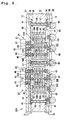
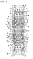
- a ceramic capacitor 100, 101 as shown in Figs. 2 to 4 or the like are accommodated in the housing opening portion 90 so as to be embedded therein.
- the ceramic capacitor 100, 101 are accommodated next to each other in the sate where the upper surface 102 (capacitor main surface) is turned to the same side as the upper surface 12 of the substrate core 11.
- the ceramic capacitor 100, 101 assumes the rectangular plate-like form or shape with the size of 12.0 mm (vertical) x12.0mm (lateral) x 0.8mm (thickness).
- the thickness of the ceramic capacitor 100, 101 is preferably 0.2mm or more to 1.0mm or less. When the thickness of the ceramic capacitor is less than 0.2mm, the ceramic capacitor 100, 101 is unable to reduce the stress arisen from at the time of mounting the IC chip 20, 21 on the IC chip mounting area 23, 24, thereby not sufficiently functioning as a support.
- the thickness of the ceramic capacitor is larger than 1.0mm, the wiring board 10 will become thick. More preferably, the thickness of the ceramic capacitor 100, 101 is 0.4 mm or more to 0.8 mm or less.
- the ceramic capacitor 100 is disposed in the area right under the IC chip mounting area 23, and the ceramic capacitor 101 is disposed in the area right below the IC chip mounting area 24.
- the dimension of the IC chip mounting area 23 (the face area where the planar connection terminals 22 of the IC chip 20 are formed) is smaller than the upper surface area 102 of the corresponding ceramic capacitor 100.
- the dimension of the IC chip mounting area 24 (the face area where the planar connection terminals 22 of the IC chip 21 are formed) is also smaller than the area of the upper surface 102 of the corresponding ceramic capacitor 101.
- the IC chip mounting area 23 is disposed within the upper surface 102 of the corresponding ceramic capacitor 100
- the IC chip mounting area 24 is disposed within the upper surface 102 of the corresponding ceramic capacitor 101.
- each ceramic capacitor 100, 101 assumes a generally square form in the plane view and includes a tapered portion having C 0.6 (R 0.6 mm) at each four corners thereof.
- the ceramic capacitor 100, 101 is so-called "a via array type ceramic capacitor".
- a ceramic sintered body 104 comprising the ceramic capacitor 100, 101 preferably has a thermal expansion coefficient, which is a mean value of the thermal expansion coefficient of the IC.chip 20, 21 and that of the built-up layer 31, 32, more preferably, the value near the thermal expansion coefficient of the IC chip 20, 21.
- the thermal expansion coefficient of the ceramic sintered body 104 is about 8-12 ppm/°C, in detail, about 9. 5 ppm /°C.
- the thermal expansion coefficient of the ceramic sintered body 104 is defined as the average value of the measured value at between 30 °C and 250 degrees °C.
- the ceramic sintered body 104 is a plate-like object having the upper surface 102 and the lower surface 103 (capacitor rear surface).
- the resin insulating layer 33 constituting the first built-up layer 31 is formed on the upper surface 102 of the ceramic sintered body 104
- the resin insulating layer 34 constituting the second built-up layer 32 is formed on the lower surface 103 of the ceramic sintered body 104.
- the ceramic sintered body 104 has a structure where a first internal electrode layer 141 and a second internal electrode layer 142 are alternately laminated by sandwiching a ceramic dielectric layer 105.
- the ceramic dielectric layer 105 is comprised of a sintered body of barium titanate, which is one of high permittivity ceramics, and functions as a dielectric (insulator) between the first internal electrode layer 141 and the second internal electrode layer 142.
- the first internal electrode layer 141 and the second internal electrode layer 142 are comprised mainly of nickel and are disposed alternately in the ceramic sintered body 104.
- a plurality of via holes 130 are formed in the ceramic sintered body 104 of the ceramic capacitor 100. These via holes 130 penetrate the ceramic sintered body 104 in the thickness direction and are disposed in a lattice pattern (an array form) over the whole surface.
- a plurality of via conductors 131, 132 comprised mainly of nickel are formed so as to communicate between the upper surface 102 and the lower surface 103 of the ceramic sintered body 104.
- Eachfirstviaconductor 131 for the power supply penetrates each first inner electrode layer 141 so that the first inner electrode layers 141 may be electrically connected to each other.
- Each first via conductor 132 for the ground penetrates each second inner electrode layer 142 so that the second inner electrode layers 142 may be electrically connected to each other.
- Each first via conductor 131 for the power supply and each first via conductor 132 for the ground are disposed in an array form as a whole. Notably, for explanatory purposes, the via conductor 131, 132 is illustrated by 3 x 3 in rows (or 5 x 5 in rows), however, the actual array has more rows.
- a plurality of first electrode terminals 111 for the power supply and a plurality of first electrode terminals 112 for the ground are formed on the upper surface 102 of the ceramic sintered body 104 of the ceramic capacitor 100 so as to protrude from the upper surface.
- a plurality of first electrode terminals 121 for the power supply and a plurality of first electrode terminals 122 for the ground are formed on the lower surface 103 of the ceramic sintered body 104 of the ceramic capacitor 100 so as to protrude from the lower surface.
- the electrode terminal 111, 112 disposed at the upper surface 102 side is electrically connected to the via conductor 47.
- the electrode terminal 121, 122 disposed at the lower surface 103 side is electrically connected to an electrode (terminal) of a motherboard (not illustrated) through the via conductor 47, the conductor layer 42, the via conductor 43, the BGA pad 48 and the solder bump 49. Further, a generally center portion of the bottom surface of the electrode terminal 111, 112 is directly connected to the end face of the via conductor 131, 132 at the upper surface 102 side. The generally center portion of the bottom surface of the electrode terminal 121, 122 is directly connected to the end face of the via conductor 131, 132 at the lower surface 103 side.
- the electrode terminal 111, 121 for the power supply is electrically conductive to the first via conductor 131 for the power supply and the first internal electrode layer 141
- the electrode terminal 112, 122 for the ground is electrically conductive to the first via conductor 132 for the ground and the second internal electrode layer 142, respectively.
- a plurality of via holes 130 are also formed in the ceramic sintered body 104 of the ceramic capacitor 101 as shown in Figs. 2 - 4.
- a plurality of via conductors 133, 134 comprised mainly of nickel is formed inside of each via hole 130 so as to communicate between the upper surface 102 and the lower surface 103 of the ceramic sintered body 104.
- Each second via conductor 133 for the power supply penetrates each first inner electrode layer 141 so that the first inner electrode layers 141 may be electrically connected to each other.
- Each second via conductor 134 for the ground penetrates each second inner electrode layer 142 so that the second inner electrode layers 142 may be electrically connected to each other.
- Each second via conductor 133 for the power supply and each second via conductor 134 for the ground are disposed in an array form as a whole. Notably, for explanatory purposes, the via conductor 133, 134 is illustrated by 3 x 3 in rows (or 5 x 5 in rows), however, the actual array has more rows.
- a plurality of second electrode terminals 113 for the power supply and a plurality of second electrode terminals 114 for the ground are formed on the upper surface 102 of the ceramic sintered body 104 of the ceramic capacitor 101 so as to protrude from the upper surface.
- a plurality of second electrode terminals 123 for the power supply and a plurality of second electrode terminals 124 for the ground are formed on the lower surface 103 of the ceramic sintered body 104 of the ceramic capacitor 101 so as to protrude from the lower surface.
- the electrode terminal 113, 114 disposed at the upper surface 102 side is electrically connected to the via conductor 47.
- the electrode terminal 123, 124 disposed at the lower surface 103 side is electrically connected to an electrode (terminal) of a motherboard (not illustrated) through the via conductor 47, the conductor layer 42, the via conductor 43, the BGA pad 48 and the solder bump 49. Further, a generally center portion of the bottom surface of the electrode terminal 113, 114 is directly connected to the end face of the via conductor 133, 134 at the upper surface 102 side. The generally center portion of the bottom surface of the electrode terminal 123, 124 is directly connected to the end face of the via conductor 133, 134 at the lower surface 103 side.
- the electrode terminal 113, 123 for the power supply is electrically conductive to the second via conductor 133 for the power supply and the first internal electrode layer 141
- the electrode terminal 114, 124 for the ground is electrically conductive to the second via conductor 134 for the ground and the second internal electrode layer 142, respectively.
- the electrode terminal 111, 112, 113, 114 is comprised mainly of nickel, and the surface thereof is entirely covered with a copper plating layer (not illustrated).
- the electrode terminal 121, 122, 123, 124 is also comprised mainly of nickel, and the surface thereof is covered with the copper plating layer (not illustrated).
- the diameter of the electrode terminals 111-114, 121-124 is about 500 ⁇ m, and the minimum pitch between the electrode terminals is about 580 ⁇ m.
- the ceramic capacitor 100, 101 functions as a capacitor.
- the first via conductor 131 for the power supply and the first via conductor 132 for the ground are al ternately adj acently disposed so that the current direction flowing through the first via conductor 131 for the power supply and the first via conductor 132 for the ground may reverse mutually.
- the second via conductor 133 for the power supply and the second via conductor 134 for the ground are alternately adjacently disposed so that the current direction flowing through the second via conductor 133 for the power supply and the second via conductor 134 for the ground may reverse mutually. As a result, reduction in the inductance is attained.
- each first via conductor 131 for the power supply is electrically connected to the planar connection terminal 22 of the IC chip 20 through a first power supply conductive path formed by the first electrode terminal 111 for the power supply, the via conductor 47, the conductor layer 42, the via conductor 43, the terminal pad 44 and the solder bump 45.
- a part of first via conductor 132 for the ground is electrically connected to the planar connection terminal 22 of the IC chip 20 through a first ground conductive path formed by the first electrode terminal 112 for the ground, the via conductor 47, the conductor layer 42, the via conductor 43, the terminal pad 44 and the solder bump 45.
- each second via conductor 133 for the power supply is electrically connected to the planar connection terminal 22 of the IC chip 21 through a second power supply conductive path formed by the second electrode terminal 113 for the power supply, the via conductor 47, the conductor layer 42, the via conductor 43, the terminal pad 44 and the solder bump 45.
- a part of second via conductor 134 for the ground is electrically connected to the planar connection terminal 22 of the IC chip 21 through a second ground conductive path formed by the second electrode terminal 114 for the ground, the via conductor 47, the conductor layer 42, the via conductor 43, the terminal pad 44 and the solder bump 45.
- the IC chip 20, 21 has an individual power supply system. Therefore, each ceramic capacitor 100, 101 is not only physically independent, but is also electrically independent from each other.
- the substrate core 11 and the ceramic capacitor 100, 101 are produced in advance with a conventionally known method, respectively.
- the substrate core 11 is produced as follows. First, a copper-clad laminated board in which a copper foil is laminated on both surfaces of a substrate having a size of 400mm (length) x 400mm (width) x 0.8mm (thickness) is prepared. In addition, the thickness of the substrate is preferably 0.2mm or more to 1.0mm or less. Next, a boring processing is performed to the copper-clad lamination using a routing machine to form a through-hole in advance in the predetermined location, which serves as the housing opening portion 90 (refer to Fig. 5).
- the through-hole serving as the housing opening portion 90 assumes a generally rectangular form cross-sectionally with a size of 14.0mm (lengthwise) x 30.0mm (crosswise) and a radius R 1.5mm at the four corners.
- the copper foil laminated on both surfaces of the copper-clad lamination board is etched to form the pattern of the conductor layer 41 by, for example, a subtractive method.
- the electrolytic copper plating is applied thereto employing the electroless copper plating layer as a common electrode.
- a dry film is laminated on thus-plated surface and subjected to an exposure and a development to thereby form predetermined pattern. In this process, unnecessary electrolytic copper plating layer, electroless copper plating layer and copper foil are removed by etching. Then, the dry film is peeled to complete the substrate core 11.
- the ceramic capacitor 100, 101 is produced as follows. A ceramic green sheet comprised of ceramics is produced, and then a nickel paste for an internal electrode layer is screen-printed on the green sheet and dried. Accordingly, a first internal electrode portion serving as the first internal electrode layer 141 and a second internal electrode portion serving as the second internal electrode layer 142 are formed. Next, the green sheet in which the first internal electrode portion is formed and the green sheet in which the second internal electrode portion is formed are alternately laminated and pressed in the laminated direction to thereby integrate the green sheets. Then, a green sheet laminated body is formed.
- a plurality of via holes 130 are formed in the green sheet laminated body using a laser processing machine, and a nickel paste for via conductor is filled in each via hole 130 using a press-fit filling equipment (not illustrated).
- a paste is printed on the upper surface of the green sheet laminated body to form the first electrode terminal 111 for the power supply and the first electrode terminal 112 for the ground (or the second electrode terminal 113 for the power supply and the second electrode terminal 114 for the ground) so as to cover the upper end face of each conductor portion at the upper side of the green sheet laminated body.
- the paste is printed on the lower surface of the green sheet laminated body to form the first electrode terminal 121 for the power supply and the first electrode terminal 122 for the ground (or the second electrode terminal 123 for the power supply and the second electrode terminal 124 for the ground) so as to cover the lower end face of each conductor portion at the lower side of the green sheet laminated body.
- the green sheet laminated body is dried so that a surface terminal portion may be solidified to some extent.
- the green sheet laminated body is degreased and subjected to firing at a predetermined temperature for a predetermined time. As a result, barium titanate and nickel contained in the paste are simultaneouslysintered, thereby forming the ceramic sintered body 104.
- the electroless copper plating (about 10 ⁇ m in thickness) is applied to each electrode terminal 111, 112, 121, 122 (or each electrode terminal 113, 114, 123, 124) which are included in the ceramic sintered body 104.
- the copper plating layer is formed on each electrode terminal 111, 112, 121, 122 (or each electrode terminal 113, 114, 123, 124), thereby completing the ceramic capacitor 100 (or the ceramic capacitor 101) .
- the electrolytic copper plating may be applied instead of applying the electroless copper plating.
- a subsequent fixation step 2 pieces of ceramic capacitors 100, 101 are accommodated in the housing opening portion 90 using a mounting device (made by Hyundai Motor Co., Ltd.) (refer to Fig. 6).
- a mounting device made by Hyundai Motor Co., Ltd.
- an adhesive tape 152 which can be peeled, is employed to seal the lower surface 13 side opening of the housing opening portion 90.
- the adhesive tape 152 is supported by a support board 151.
- Each ceramic capacitor 100, 101 is stuck on an adhesive face 153 of the adhesive tape 152 to be temporarily fixed.
- the gap between the inner surface of the housing opening portion 90 and the side face 106 of the ceramic capacitor 100, 101, and the region between the adjacent ceramic capacitor 100, 101 is filled with a filler 92 made of thermosetting resin (underfill material, made by Namix Co., Ltd.) using a dispenser device (made by Asymtek). Then, the filler 92 is hardened in a heat treatment to fix the ceramic capacitor 100, 101 to the housing opening portion 90. Then, the adhesive tape 152 is peeled at this time.
- a filler 92 made of thermosetting resin underfill material, made by Namix Co., Ltd.
- a built-up layer formation step is conducted.
- the first built-up layer 31 is formed on the upper surface 12 and the upper surface 102
- the second built-up layer 32 is formed on the lower surface 13 and the lower surface 103, based on the conventionally known method.
- the wiring board 10 comprised of the substrate core 11, the built-up layer 31, 32 is completed.
- the photosensitive epoxy resin is laminated on the lower surface 13 and the lower surface 103.
- an exposure and development are performed on thus-upper and lower surfaces to forma resin insulating layer 33, 34 of the first layer, respectively.
- the resin insulating layer 33, 34 has a blind via in a location where the via conductor 47 is formed. Further, a boring processing is performed using a YAG laser or a carbon dioxide laser to form a through-hole penetrating substrate core 11 and the resin insulating layer 33, 34. Then, after forming a through-hole conductor 16 by performing electroless copper plating and electrolytic copper plating in accordance with the conventionally known method, a plugging body 17 is filled in the through-hole conductor 16.
- the electrolytic copper plating is performed in accordance with the conventionally known method (e.g., semiadditive method) so as to form the via conductor 47 inside of the blind via, as well as forming the conductor layer 42 serving as a second layer on the resin insulating layer 33, 34 serving as the first layer.
- the conventionally known method e.g., semiadditive method
- the photosensitive epoxy resin is laminated on the resin insulating layer 33, 34 serving as the first layer, and the exposure and development thereof is performed to form the resin insulating layer 35, 36 of a second layer which has a blind via in the location where the via conductor 43 is formed.
- the electrolytic copper plating is applied in accordance with the conventionally known method to form the via conductor 43 inside of the blind via and to form a terminal pad 44 on the resin insulating layer 35 serving as the second layer and a pad 48 for BGA is formed on the resin insulating layer 36 serving as the second layer.
- a solder resist 37, 38 are formed on the resin insulating layer 35, 36 serving as the second layer by applying the photosensitive epoxy resin and curing thereof.
- the exposure and development are performed in the state where the predetermined mask is disposed to pattern-print an opening 40, 46 on the solder resist 37, 38.
- a solder bump 45 is formed on the terminal pad 44, and a solder bump 49 is formed on the pad 48 for BGA.
- the wiring board 10 comprised of the substrate core 11 and the built-up layer 31, 32 is completed.
- a wiring board 10A includes two housing opening portions 91 which open at the upper surface 12 of the substrate core 11.
- Each ceramic capacitor 100, 101 is accommodated in each housing opening portion 91, respectively, in the state where the upper surface 12 and the upper surface 102 are turned to the same side.
- the substrate core 11 includes a through-hole conductor 16A (conductor portion) disposed in an area formed between the adjoining housing opening portions 91.
- the inside of the through-hole conductor 16, 16A is filled with, for example, a plugging body 17 such as an epoxy resin.
- the upper end of the through-hole conductor 16, 16A is electrically connected to the conductor layer 42 formed on the resin insulating layer 33 of the first built-up layer 31, and the lower end of the through-hole conductor 16, 16A is electrically connected to the conductor layer 42 formed on the resin insulating layer 34 of the second built-up layer 32. That is, the through-hole conductor 16, 16A has a function to electrically connect the first built-up layer 31 and the second built-up layer 32.
- the through-hole conductor 16A formed between the adjoining housing opening portions 91 is formed simultaneously with other through-hole conductors 16 by means of the same method as that of the through-hole conductor 16 of the first embodiment.
- the space for forming the through-hole conductor 16A can be easily secured in the area formed between the adjoining ceramic capacitors 100, 101.
- a wiring of the conductor layer used for electrically connecting the top and rear surfaces of the substrate core 11 can be formed easily.
- any conductor for signals is not necessarily formed in the ceramic capacitor 100, 101 or the substrate core 11. Therefore, the miniaturization of the ceramic capacitor 100, 101 or the substrate core 11 may be facilitated. Furthermore, the miniaturization of ceramic capacitor 100, 101 contributes to an easy formation of the through-hole conductor 16A because the enough space for forming the through-hole conductor 16A can be secured.
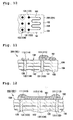
- a conductor portion such as a through-hole conductor 16B (see the wiring board 10B in Fig. 9) may be formed in the filler 92 which fills the area formed between the adjoining ceramic capacitors 100, 101.
- This structure facilitates the easy wiring of the conductor layer for electrically connecting the rear and top surfaces of the substrate core 11.
- the through-hole conductor 16B in the filler 92 is formedasfollows. Thatis,athrough-holepenetratingthesubstrate core 11 and the resin insulating layer 33, 34 and a through-hole penetrating the filler 92 are formed simultaneously by a laser boring processing. Then, an electroless copper plating and an electrolytic copper plating are applied by the conventionally known method so as to form the through-hole conductor 16B in the filler 92 which fills the area formed between the ceramic capacitor 100, 101.
- the housing opening portion 90, 91 of each embodiment described above is a through-hole portion which opens at the upper surface 12 and the lower surface 13 of the substrate core 11.
- the housing opening portion 90, 91 may be a bottomed concave portion (non-through-hole portion), which opens only at the upper surface 12 of the substrate core 11.
- a wiring pattern (inner layer pattern) may be formed in the substrate core 11 according to each embodiment described above. With this structure, a complicated electric circuit can be formed inside of the wiring board 10, thereby facilitating much more advanced features of the wiring board 10. Further, the substrate core 11 may be formed in such a manner that a thin insulating layer is laminated on the core.
- a resistive element 161 may be formed on an upper surface 102 or the like of a ceramic capacitor 200, 201.
- the resistive element 161 electrically connects a first electrode terminal 111 for the power supply (second electrode terminal 113 for the power supply) and the other first electrode terminal 111 for the power supply (second electrode terminal 113 for the power supply).
- the resistive element 161 is comprised of ceramics having a higher resistance than that of a material constituting the electrode terminal 111, 113 for the power supply, the first inner electrode layer 141 and the second inner electrode layer 142.
- the suitable resistive element 161 is formed such that, for example, after completion of the ceramic capacitor 200, 201, a ceramic paste is applied to the upper surface 102 side and fired for a predetermined duration, and then adjusting resistance value or the like by removing an unnecessary portion.
- the resistive element is necessarily embedded in a location in the substrate core 11 other than in the ceramic capacitor 200, 201, or formed at the built-up layer 31, 32 side.
- a plurality of dummy-via electrodes may be disposed between the ceramic capacitors 100, 101.
- the noise caused by interference between the ceramic capacitor 100 and the ceramic capacitor 101 can be reduced.
- the ceramic capacitor 100, 101 contains a large capacity portion and the small capacity portion whose capacity is smaller than the large capacity portion, it is preferable to provide plural dummy-via electrodes (groundviaelectrodes) between the large capacity portion and the small capacity portion.
- a plurality of dummy-via electrodes may be disposed in a location surrounding the ceramic capacitor 100, 101.
- a side face dummy electrode 151, 152 may be formed in a face (i.e., side face 106) other than the upper surface 102 and the lower surface 103 of a ceramic capacitor 100C, 101C. Similar to the above embodiment, this structure also contributes to a reduction in noise caused by interference between the ceramic capacitors 100C, 101C.
- the side face dummy electrode 151, 152 shown in Fig. 13 may be a conductor which is not electrically connected to any conductor layers. However, preferably, the side face dummy electrode 151, 152 is electrically connected to, for example, the conductor layer for the ground in the built-up layer 31, 32. According to this structure, the shielding effectiveness can be improved.
- such side face dummy electrode 151, 152 is comprised of, for example, the same metal material as that of the electrode terminal provided in the ceramic capacitor 100C, 101C.
- a capacitor portion 162 of a separate system (for the power supply to I/O or the like) other than for the IC chip 20, 21 may be formed in a part of a ceramic capacitor 300, 301. This structure allows the wiring board 10 to have more advanced features.
Landscapes
- Engineering & Computer Science (AREA)
- Power Engineering (AREA)
- Microelectronics & Electronic Packaging (AREA)
- Physics & Mathematics (AREA)
- Electromagnetism (AREA)
- Manufacturing & Machinery (AREA)
- Production Of Multi-Layered Print Wiring Board (AREA)
- Ceramic Capacitors (AREA)
- Fixed Capacitors And Capacitor Manufacturing Machines (AREA)
Abstract
Description
- The present invention is related to a wiring board having a structure wherein a ceramic capacitor is embedded in a substrate core and a built-up layer is laminated on a surface of the substrate core on which a semiconductor integrated circuit element is mounted.
- In recent years, the semiconductor integrated circuit element (IC chip) used for CPU in a computer etc. has operated at higher speeds with high functioning features. Along with this advance, the number of terminals increases and the terminal interval tends to be narrow. Generally, many terminals are densely formed on the bottom surface of the IC chip in an array form, and such a terminal block is connected to a terminal block at the motherboard side by flip chip connection. However, since the pitch between the terminal block at the IC chip side and the terminal block at the motherboard side has a great difference, it is difficult to directly connect the IC chip to the motherboard. Therefore, the connection method generally employed is such that a package constituted by the IC chip, which is mounted on a wiring board for mounting the IC chip, is produced and then mounted on the mother board. An example of such wiring boards for mounting the IC chip, which constitutes this type of package, includes a wiring board where a ceramic chip is embedded in a core substrate, which is comprised of a polymer material, so as to form a core portion, and a built-up layer is formed on both top and rear surfaces of the core portion, respectively (e.g., see
Japanese Patent Application Laid-Open (kokai) No. 2005-39243 - Recently, the strong demand for a system capable of offering a higher performance than a package where only a single microprocessor is mounted has been increasing. One of the examples for such system includes a package having a plurality of microprocessors. That is, this type of package having such multi-microprocessor structure is capable of performing a parallel processing of plural threads (tasks), which a single microprocessor structure or the like cannot perform, resulting in improving the processing capacity of the entire system. Further, a failure-resistance of the multi-microprocessor structure is improved compared to the single microprocessor structure.
- When carrying out a package having a multi-microprocessor structure, fore xample, aceramic capacitor in a wiring board according to
Japanese Patent Application Laid-Open (kokai) No. 2005-39243 - Further, the wiring board according to
Japanese Patent Application Laid-Open (kokai) No.2005-39243 - In this type of package, since the calorific power of the microprocessor also increases, it is very important to match the coefficient of thermal expansion between the microprocessor and the wiring board. That is, when the thermal expansion coefficient between the microprocessor and the wiring board does not match, substantial heat stress will be imposed on a microprocessor, and a crack and a faulty connection tends to occur in the microprocessor. Therefore, it is necessary to adopt the structure which can reduce the influence of such heat stress.
- The present invention has been accomplished in view of the above problems, and an object of the invention is to provide a wiring board capable of bringing out the advantages of the structure where a plurality of semiconductor integrated circuit elements are mounted, and the wiring board which allows a reduction in size thereof and offers excellent cost performance and reliability.
- In light of the above, the present invention provides the wiring board according to independent claim 1.
- Further advantages, features, aspects and details of the invention are evident from the dependent claims, the description and the drawings.
- A means for solving the above-mentioned problem is a wiring board, comprising: a substrate core including a core main surface and a core rear surface; a plurality of ceramic capacitors having a capacitor main sur face and a structure where a first inner electrode layer and a second inner electrode layer are alternately laminated by sandwiching a ceramic dielectric layer, wherein said ceramic capacitor is embedded in said substrate core in the state where said core main surface and said capacitor main surface are turned to the same side; and a built-up layer having a structure where an inter layer insulating layer and a conductor layer are alternately laminated on said core main surface and said capacitor main surface, and including a plurality of semiconductor integrated circuit element mounting areas in various locations on a surface of said built-up layer, and wherein said plural ceramic capacitors are disposed in areas of said substrate core, which correspond to said plural semiconductor integrated circuit element mounting areas.
- Therefore, according to the wiring board of the above described means, a plurality of semiconductor integrated circuit element mounting areas on which a semiconductor integrated circuit element may be mounted is provided in the built-uplayer, and, in the substrate core, a plurality of ceramic capacitors are disposed in the areas corresponding to a plurality of semiconductor integrated circuit element mounting areas, respectively. Therefore, a conductor portion, such as a through-hole conductor or a conductor pattern or the like can be formed in an area formed between the adjoining ceramic capacitors. As a result, even though it is a case where the structure of mounting a plurality of semiconductor integrated circuit elements is adopted, a conductor layer can be formed for establishing an electrical connection between the top and rear surfaces of the substrate core, resulting in a prevention of an enlargement of the overall size of the wiring board.
- Further, even if a power supply system of plural semiconductor integrated circuit elements cannot be shared and an individual power supply system for each semiconductor integrated circuit element is necessary, each semiconductor integrated circuit element can fully operate because the plural ceramic capacitors are electrically connected to the semiconductor integrated circuit element mounting areas, respectively. Therefore, when adopting the structure of mounting a plurality of semiconductor integrated circuit elements, the advantages of such a structure can be fully realized.
- Furthermore, according to this structure, each semiconductor integrated circuit element is supported on each ceramic capacitor. Thus, compared to the conventional structure where each semiconductor integrated circuit element is supported on a single large ceramic capacitor, the influence of heat stress is reduced because a thermal expansion coefficient with the semiconductor integrated circuit element can easily match. Therefore, a crack and a faulty connection of the semiconductor integrated circuit element due to great heat stress can be prevented.
- As mentioned above, in the substrate core, a plurality of ceramic capacitors are disposed in the areas corresponding to a plurality of semiconductor integrated circuit element mounting areas, respectively. The terms "the areas corresponding to a plurality of semiconductor integrated circuit element mounting areas" here means an inner area present and corresponding to a plurality of semiconductor integrated circuit element mounting areas. Speaking more concretely, each ceramic capacitor is disposed, respectively, in the inner area of the substrate core which is situated generally directly below the plural semiconductor integrated circuit element mounting area. Each ceramic capacitor disposed in this way is provided so that a part of or the entire ceramic capacitor may overlap the semiconductor integrated circuit element mounting area, when looking from the thickness direction of the capacitor. In addition, correlation in the magnitude between the dimension of each ceramic capacitor when looking from the thickness direction of the capacitor and the dimension of each semiconductor integrated circuit element mounting area can be at one's discretion. However, it is preferable that the former dimension be equal to or lager than the latter dimension.
- Here, "semiconductor integrated circuit element" in the present invention means mainly a semiconductor integrated circuit element used as a microprocessor or the like of a computer. The semiconductor integrated circuit element is, for example, flip chip connected to the semiconductor integrated circuit element mounting area. Notably, "semiconductor integrated circuit element mounting area" means an area where a terminal pad block is disposed on the surface of the built-up layer. Two or more semiconductor integrated circuit elements mounting areas (i.e., the number of semiconductor integrated circuit element) may be provided.
- The substrate core constituting the above-mentioned wiring board is a part of the core portion in the wiring board, and assumes, for example, a plate-like form or shape having the core main surface and the core rear surface located opposed to the core main surface. The substrate core may include one ormore housing opening portion (s) for accommodating the ceramic capacitor. The housing opening portion may be a non-through-hole which only opens at the core main surface, or may be a through-hole which opens at both core main surface and core rear surface.
- Although the material for forming the substrate core is not limited, a preferable substrate core is comprised mainly of a polymer material. Examples of the polymer materials for forming the substrate core include EP resin (epoxyresin), PI resin (polyimide resin), BT resin (bismaleimide triazine resin), PPE resin (polyphenylene ether resin), etc. Notably, a composite material made of these resins and organic fibers, such as glass fiber (glass woven fabric and non-woven glass fabric) or polyamide fiber may be employed.
- The ceramic capacitor constituting the above-mentioned wiring board has the capacitor main surface and a structure where the first inner electrode layer and the second inner electrode layer are alternately laminated by sandwiching the ceramic dielectric layer. Preferably, the ceramic capacitor includes a capacitor main surface and a capacitor rear surface, which is located opposite side of the capacitor main surface. The ceramic capacitor in the present invention includes a capacitor formed in such a manner that a thin film layer made of ceramic material is laminated on a substrate (not limited to ceramic substrate). The ceramic capacitor is embedded in the substrate core in the state where the core main surface and the capacitor main surface are turned to the same side. The terms "embedded" here means the state where at least a part of a ceramic capacitor is accommodated in the housing opening portion of the substrate core or the state where the entire ceramic capacitor is accommodated in the housing opening portion of the substrate core. Further, the ceramic capacitor is fixed by a filler made from, for example, a polymer material in the state that the ceramic capacitor is embedded in the substrate core.
- Although two or more ceramic capacitors may be provided, the same number as the number of semiconductor integrated circuit element mounting areas is preferable. Constituting this way, all the ceramic capacitors can be electrically connected to all semiconductor integrated circuit element mounting areas. Further, a suitable example of the ceramic capacitor includes a via arrayed type ceramic capacitor. Namely, the ceramic capacitor includes a plurality of via conductors for the power supply which electrically connect the said first inner electrode layers, and a plurality of via conductors for the ground which electrically connect the second inner electrode layers. The plural via conductors for the power supply and the plural via conductors for the ground are preferably disposed in an array form as a whole. That is, the plural via conductors for the power supply and the plural via conductors for the ground together are preferably disposed as an array. When employing this structure, a reduction in size of the ceramic capacitor is facilitated, thereby facilitating a reduction in the overall size of the wiring board. Furthermore, despite its compact size, high electric capacity may be relatively easily secured, resulting in establishing more stable power supply.
- Notably, when the substrate core has a plurality of housing opening portions therein which open at the core main surface, the ceramic capacitor is preferably accommodated in each housing opening portion in the state where the core main surface and the capacitor main surface are turned to the same side. With this structure, it is easy to secure the area for forming the conductor portion such as a through-hole conductor or a conductor pattern in the area formed between the adjoining housing opening portions. As a result, even though the structure of mounting plural semiconductor integrated circuit elements is adopted, a wiring of the conductor layer used for electrically connecting the top and rear surfaces of the substrate core becomes easy. That is, the substrate core may include the conductor portion, which is used for electrically connecting the core main surface and the core rear surface, in the area formed between the adjoining housing opening portions.
- On the other hand, when the substrate core includes only a single housing opening portion therein, which opens at the core main surface, the plural ceramic capacitors are preferably accommodated in the housing opening portion in the state where the core main surface and the capacitor main surface are turned to the same side. With this structure, the formation of the substrate core becomes easy be cause the same number of housing opening portions as that of the ceramic capacitor is not necessarily formed when all the ceramic capacitors are to be accommodated, resulting in easy formation of the wiring board. Notably, the substrate core may include the conductor portion, which is used for electrically connecting the core main surface and the core rear surface, in the area formed between the adjoining ceramic capacitors. In this case, the area formed between the adjoining ceramic capacitors is filled by the filler, and the conductor portion, such as a through-hole conductor or a conductor pattern is formed in the filler. The filler preferably comprises a resin material having an insulating characteristic.
- The aforementioned conductor portion, such as a through-hole conductor or a conductive pattern is preferably electrically connected to, for example, the conductor layer for signals in the wiring board. In this case, design flexibility for wiring can be improved. Alternately, the conductor portion such as a through-hole conductor or a conductive pattern is preferably electrically connected to, for example, the conductor layer for the ground. According to this structure, because the shielding effectiveness can be obtained, an interference arising between the ceramic capacitors can be prevented, and a noise caused by the interference can be reduced. When the conductor portion is the through-hole conductor, the plural through-hole conductors are preferably disposed in rows so that higher shielding effectiveness may be attained. In addition, the conductor portion can be a dummy conductor layer, which is electrically connected to neither the conductor layers for signals, for the power supply nor for the ground.
- A sintered body of high-temperature-firing ceramics, such as alumina, aluminum nitride, boron nitride, silicon carbide and silicon nitride, is preferably employed as a ceramic dielectric layer. Also, a sintered body of low-temperature-firing ceramics, such as a glass-ceramic formed in such a manner that inorganic ceramic fillers, such as alumina, is added to borosilicic acid system glass or lead borosilicate system glass is preferably employed as a ceramic dielectric layer. In this case, it is also preferable to employ a sintered body of dielectric ceramics, such as barium titanate, lead titanate and strontium titanate, according to a use. When the sintered body of dielectric ceramics is employed, a ceramic capacitor with a large electrostatic capacitance can be expected.
- The material for forming the first inner electrode layer and the second inner electrode layer is not particularly limited, however, a metal which can be sintered simultaneously with ceramics, for example, nickel, molybdenum, tungsten, titanium or the like is suitable. In addition, when the sintered body of low-temperature-firing ceramics is adopted, copper, silver or the like can be employed as a material for forming the first inner electrode layer and the second inner electrode layer.
- The ceramic capacitor may include a resistive element which comprises a material having a higher resistance value than the material constituting the first inner electrode layer and said second inner electrode layer. With this structure, for example, various potential can be established within the same ceramic capacitor, thereby facilitating advanced features of the wiring board. When no resistive element is formed in the ceramic capacitor, the resistive element must be provided in a separate location from the ceramic capacitor in the substrate core, or provided at the built-up layer side, resulting in it being hard to form the resistive element. In addition, a material for forming the resistive element may be a conductive material having a higher resistance value than that of the first inner electrode layer and the second inner electrode layer. The examples of such material include a metal material, ceramic material or the like.
- The built-up layer constituting the wiring board has a structure where an interlayer insulating layer, which comprised mainlyofapolymermaterial, and the conductor layer are alternately laminated. Although the-built-up layer (first built-up layer) may be formed only on the core main surface and the capacitor main surface, a second built-up layer having a structure where the interlayer insulating layer and the conductor layer are alternately laminated may be formed on the core rear surface and the capacitor rear surface. With this structure, an electric circuit can be formed not only in the first built-up layer but also in the second built-up layer, thereby facilitating much more advanced features of the wiring board.
- Notably, the built-up layer (first built-up layer) formed on the core main surface and the capacitor main surface includes a plurality of semiconductor integrated circuit element mounting areas in various locations of the surface of the built-up layer. Since a semiconductor element can be mounted on such semiconductor integrated circuit element mounting area, the difference in thermal expansion coefficient with the semiconductor integrated circuit element can be reduced, compared with the case where the semiconductor integrated circuit element mounting area is formed on the substrate core. Thus, this structure facilitates a reduction in the influence of the thermal stress imposed on the semiconductor integrated circuit element.
- In addition, the dimension of the semiconductor integrated circuit element mounting area is established so as to be equal to or smaller than the dimension of the capacitor main surface of the corresponding ceramic capacitor. The semiconductor integrated circuit element mounting area is preferably located within the capacitor main surface of the corresponding ceramic capacitor, when looking from the thickness direction of the ceramic capacitor. With this structure, since the semiconductor integrated circuit element mounting area is located in the area right above the ceramic capacitor,thesemiconductorintegrated circuitelement mounted on the semiconductor integrated circuit element mounting area is supported by the ceramic capacitor having high rigidity and a small coefficient of thermal expansion. Therefore, in the semiconductor integrated circuit element mounting area, the built-up layer is unlikely to deform, thereby being able to stably support the semiconductor integrated circuit element mounted on the semiconductor integrated circuit element mounting area. As described above, the dimension of the semiconductor integrated circuit element mounting area is smaller than that of capacitor main surface of the corresponding ceramic capacitor. Preferably, the dimension of the semiconductor integrated circuit element mounting area is, in detail, 90% or less of the dimension of the capacitor main surface, the most preferably, 50% or more to 90% orless. When the dimension of the semiconductor integratedcircui t element mounting area is 90% or less, the semiconductor integrated circuit element can be easily and stably supported. Further, when the dimension of the semiconductor integrated circuit element mounting area is 50% or more, the dimension of the semiconductor integrated circuit element mounting area will not be too small.
- According to another aspect, a wiring board is provided, which is capable of fully bringing out the advantages of the structure where a plurality of semiconductor integrated circuit elements are mounted, and the wiring board which allows a reduction in size thereof and offers excellent cost performance and reliability.
- The wiring board includes a substrate core, a ceramic capacitor and a built-up layer. The substrate core has a housing opening portion therein which opens at a core main surface. The ceramic capacitor is accommodated in the housing opening portion in the state where the core main surface and a capacitor main surface are turned to the same side. The built-up layer includes a semiconductor integrated circuit element mounting area in various locations on a surface thereof. In the substrate core, each ceramic capacitor is disposed in an area corresponding to each semiconductor integrated circuit element mounting area, respectively.
- Embodiments according to the invention are also directed to methods by which the described apparatus is manufactured. It includes method steps for carrying out every function of the apparatus or manufacturing every part of the apparatus.
- The invention will be better understood by reference to the following description of embodiments of the invention taken in conjunction with the accompanying drawings, wherein:
- Fig. 1 is a schematic sectional view showing a wiring board according to a first embodiment for carrying out the present invention.
- Fig. 2 is a schematic sectional view showing a ceramic capacitor.
- Fig. 3 is a schematic explanatory view showing the connection in an inner layer of a ceramic capacitor.
- Fig. 4 is a schematic explanatory view showing the connection in an inner layer of a ceramic capacitor.
- Fig. 5 is an explanatory view showing a manufacturing method of a wiring board.
- Fig. 6 is an explanatory view showing a manufacturing method of a wiring board.
- Fig. 7 is an explanatory view showing a manufacturing method of a wiring board.
- Fig. 8 is a schematic sectional view showing a ceramic capacitor according to a second embodiment.
- Fig. 9 is a schematic sectional view showing a ceramic capacitor according to another embodiment.
- Fig. 10 is a schematic plan view of a ceramic capacitor showing a vicinity of resistive element according to another embodiment.
- Fig. 11 is a schematic sectional view of a ceramic capacitor showing a vicinity of resistive element.
- Fig. 12 is a schematic sectional view of a ceramic capacitor showing a vicinity of resistive element.
- Fig. 13 is a schematic sectional view showing a wiring board according to another embodiment.
- Fig. 14 is a schematic plan view of a ceramic capacitor showing a vicinity of capacitor portion according to another embodiment.
- Hereafter, a first embodiment for carrying out a wiring board of the present invention will be described in detail with reference to the drawings.
- As shown in Fig. 1, a
wiring board 10 according to the present embodiment is a wiring board for mounting an IC chip, and comprising: asubstrate core 11 comprised of glass epoxy and assuming a generally rectangular form; a first built-up layer 31 (built-up layer) formed on an upper surface 12 (core main surface) of thesubstrate core 11; and a second built-uplayer 32 formed on an lower surface 13 (core rear surface) of thesubstrate core 11. A through-hole conductor 16 is formed in plural locations in thesubstrate core 11. The through-hole conductor 16 electrically connects between theupper surface 12 side and thelower surface 13 side of thesubstrate core 11. Inaddition,insideofthethrough-holeconductor 16 is filled with, for example, a pluggingbody 17, such as epoxy resin. Moreover, aconductor layer 41 comprised of copper is formed in a pattern on theupper surface 12 and thelower surface 13 of thesubstrate core 11 so that eachconductor layer 41 may be electrically connected to the through-hole conductor 16. - The first built-up
layer 31 formed on theupper surface 12 of thesubstrate core 11 has a structure whereresin insulating layers 33, 35 (hereinafter referred to as an interlayer insulating layer) comprised of epoxy resin and aconductor layer 42 comprised of copper are alternately laminated. In this embodiment, a thermal expansion coefficient of the first built-uplayer 31 is about 30-40 ppm/°C, indetail, about 35 ppm/°C. The thermal expansion coefficient of the first built-uplayer 31 is defined as an average value of the measured value at between 30°C and a glass-transition temperature (Tg). A part of theconductor layer 42 formed on the surface of theresin insulating layer 33 serving as a first layer is electrically connected to an upper end of the through-hole conductor 16.Terminal pads 44 are formed in plural locations on the surface of the secondresin insulating layer 35 in an array form. Moreover, the surface of theresin insulating layer 35 is almost entirely covered with a solder resist 37.Openings 46 to which theterminal pads 44 are exposed are formed in the predetermined locations of the solder resist 37. Plural solder bumps 45 are disposed on the surfaces of theterminal pads 44, respectively. Eachsolder bump 45 is electrically connected toplanar connection terminals 22 ofIC chips 21, 22 (semiconductor integrated circuit element), respectively. The IC chips 20, 21 according to the present embodiment assume a rectangular plate-like form or shape and are comprised of silicon having a thermal expansion coefficient of about 3.5 ppm/°C. In addition, in the first built-uplayer 31, eachterminal pad 44 and eachsolder bump 45 are located within an area right above aceramic capacitor chip mounting area 23, 24 (a semiconductor integrated circuit element mounting area). The ICchip mounting area top surface 39 of the first built-uplayer 31. Moreover, theresin insulating layers conductors conductors terminal pad 44 are electrically connected through these conductors. - As shown in Fig. 1, the second built-up
layer 32 formed on thelower surface 13 of thesubstrate core 11 has the almost same structure as that of the first built-uplayer 31. That is, the second built-uplayer 32 has a thermal expansion coefficient of about 30-40 ppm/°C and has a structure whereresin insulating layers 34, 36 (hereinafter referred to as an interlayer insulating layer) comprised of epoxy resin and aconductor layer 42 are alternately laminated. Apart ofconductor layer 42 formed on the lower surface of theresin insulating layer 34 serving as the first layer is electrically connected to the lower end of the through-hole conductor 16.BGA pad 48 electrically connected to theconductor layer 42 through the viaconductor 43 is formed in plural locations on the lower surface of the secondresin insulating layer 36 with a lattice pattern. Moreover, the lower surface of theresin insulating layer 36 is almost entirely covered with a solder resist 38.Openings 40 to which theBGApads 48 are exposed are formed in the predetermined locations of the solder resist 38. Plural solder bumps 49 for electrically connecting to a motherboard (not illustrated) are disposed on the surfaces of theBGA pads 48, respectively. Then, thewiring board 10 is mounted on the motherboard (not illustrated) through eachsolder bump 49. - The thermal expansion coefficient of the
substrate core 11 is about 10-15 ppm/°C in the planar direction (XY direction). In addition, the thermal expansion coefficient of thesubstrate core 11 is defined as the average value of the measured value at between 30 °C and a glass-transition temperature (Tg). Thesubstrate core 11 has a rectangular-shapedhousing opening portion 90 in a plane view which opens at each center portion of theupper surface 12 and thelower surface 13. That is, thehousing opening portion 90 is a through-hole portion. Aceramic capacitor housing opening portion 90 so as to be embedded therein. In addition, theceramic capacitor upper surface 12 of thesubstrate core 11. Theceramic capacitor ceramic capacitor ceramic capacitor IC chip chip mounting area wiring board 10 will become thick. More preferably, the thickness of theceramic capacitor substrate core 11, theceramic capacitor 100 is disposed in the area right under the ICchip mounting area 23, and theceramic capacitor 101 is disposed in the area right below the ICchip mounting area 24. The dimension of the IC chip mounting area 23 (the face area where theplanar connection terminals 22 of theIC chip 20 are formed) is smaller than theupper surface area 102 of the correspondingceramic capacitor 100. Similarly, the dimension of the IC chip mounting area 24 (the face area where theplanar connection terminals 22 of theIC chip 21 are formed) is also smaller than the area of theupper surface 102 of the correspondingceramic capacitor 101. When looking from the thickness direction of theceramic capacitor chip mounting area 23 is disposed within theupper surface 102 of the correspondingceramic capacitor 100, and the ICchip mounting area 24 is disposed within theupper surface 102 of the correspondingceramic capacitor 101. - As shown in Fig. 1, the gap between the inner surface of the
housing opening portion 90 and theside face 106 of theceramic capacitor filler 92 comprised of a polymer material (thermosetting resin, such as epoxy resin, in this embodiment). Thefiller 92 fixes eachceramic capacitor substrate core 11 as well as having a function of absorbing the deformation in the planar direction and the thickness direction of theceramic capacitor substrate core 11 by its own elastic deformation. In addition, eachceramic capacitor filler 92 deforms due to a temperature variation, the stress concentration to the corners of eachceramic capacitor filler 92. - As shown in Figs. 1 - 4, the
ceramic capacitor sintered body 104 comprising theceramic capacitor IC.chip layer IC chip sintered body 104 is about 8-12 ppm/°C, in detail, about 9. 5 ppm /°C. The thermal expansion coefficient of the ceramicsintered body 104 is defined as the average value of the measured value at between 30 °C and 250 degrees °C. Further, the ceramicsintered body 104 is a plate-like object having theupper surface 102 and the lower surface 103 (capacitor rear surface). Inaddition, theresin insulating layer 33 constituting the first built-uplayer 31 is formed on theupper surface 102 of the ceramicsintered body 104, and theresin insulating layer 34 constituting the second built-uplayer 32 is formed on thelower surface 103 of the ceramicsintered body 104. The ceramicsintered body 104 has a structure where a firstinternal electrode layer 141 and a secondinternal electrode layer 142 are alternately laminated by sandwiching aceramic dielectric layer 105. Theceramic dielectric layer 105 is comprised of a sintered body of barium titanate, which is one of high permittivity ceramics, and functions as a dielectric (insulator) between the firstinternal electrode layer 141 and the secondinternal electrode layer 142. The firstinternal electrode layer 141 and the secondinternal electrode layer 142 are comprised mainly of nickel and are disposed alternately in the ceramicsintered body 104. - As shown in Figs. 2-4, a plurality of via
holes 130 are formed in the ceramicsintered body 104 of theceramic capacitor 100. These viaholes 130 penetrate the ceramicsintered body 104 in the thickness direction and are disposed in a lattice pattern (an array form) over the whole surface. In each viahole 130, a plurality of viaconductors upper surface 102 and thelower surface 103 of the ceramicsintered body 104.Eachfirstviaconductor 131 for the power supply penetrates each firstinner electrode layer 141 so that the first inner electrode layers 141 may be electrically connected to each other. Each first viaconductor 132 for the ground penetrates each secondinner electrode layer 142 so that the second inner electrode layers 142 may be electrically connected to each other. Each first viaconductor 131 for the power supply and each first viaconductor 132 for the ground are disposed in an array form as a whole. Notably, for explanatory purposes, the viaconductor - As shown in Figs. 2-4, a plurality of
first electrode terminals 111 for the power supply and a plurality offirst electrode terminals 112 for the ground are formed on theupper surface 102 of the ceramicsintered body 104 of theceramic capacitor 100 so as to protrude from the upper surface. Also, a plurality offirst electrode terminals 121 for the power supply and a plurality offirst electrode terminals 122 for the ground are formed on thelower surface 103 of the ceramicsintered body 104 of theceramic capacitor 100 so as to protrude from the lower surface. Theelectrode terminal upper surface 102 side is electrically connected to the viaconductor 47. On the other hand, theelectrode terminal lower surface 103 side is electrically connected to an electrode (terminal) of a motherboard (not illustrated) through the viaconductor 47, theconductor layer 42, the viaconductor 43, theBGA pad 48 and thesolder bump 49. Further, a generally center portion of the bottom surface of theelectrode terminal conductor upper surface 102 side. The generally center portion of the bottom surface of theelectrode terminal conductor lower surface 103 side. Therefore, theelectrode terminal conductor 131 for the power supply and the firstinternal electrode layer 141, and theelectrode terminal conductor 132 for the ground and the secondinternal electrode layer 142, respectively. - Similarly, a plurality of via
holes 130 are also formed in the ceramicsintered body 104 of theceramic capacitor 101 as shown in Figs. 2 - 4. A plurality of viaconductors hole 130 so as to communicate between theupper surface 102 and thelower surface 103 of the ceramicsintered body 104. Each second viaconductor 133 for the power supply penetrates each firstinner electrode layer 141 so that the first inner electrode layers 141 may be electrically connected to each other. Each second viaconductor 134 for the ground penetrates each secondinner electrode layer 142 so that the second inner electrode layers 142 may be electrically connected to each other. Each second viaconductor 133 for the power supply and each second viaconductor 134 for the ground are disposed in an array form as a whole. Notably, for explanatory purposes, the viaconductor - Then, a plurality of
second electrode terminals 113 for the power supply and a plurality ofsecond electrode terminals 114 for the ground are formed on theupper surface 102 of the ceramicsintered body 104 of theceramic capacitor 101 so as to protrude from the upper surface. Also, a plurality ofsecond electrode terminals 123 for the power supply and a plurality ofsecond electrode terminals 124 for the ground are formed on thelower surface 103 of the ceramicsintered body 104 of theceramic capacitor 101 so as to protrude from the lower surface. Theelectrode terminal upper surface 102 side is electrically connected to the viaconductor 47. On the other hand, theelectrode terminal lower surface 103 side is electrically connected to an electrode (terminal) of a motherboard (not illustrated) through the viaconductor 47, theconductor layer 42, the viaconductor 43, theBGA pad 48 and thesolder bump 49. Further, a generally center portion of the bottom surface of theelectrode terminal conductor upper surface 102 side. The generally center portion of the bottom surface of theelectrode terminal conductor lower surface 103 side. Therefore, theelectrode terminal conductor 133 for the power supply and the firstinternal electrode layer 141, and theelectrode terminal conductor 134 for the ground and the secondinternal electrode layer 142, respectively. - As shown in Fig. 2, the
electrode terminal electrode terminal - When a voltage is applied to the first
internal electrode layer 141 and the secondinternal electrode layer 142 through theelectrode terminal 121, 122 (or theelectrode terminal 123, 124) from the motherboard side, the positive charge will be accumulated in, for example, the firstinternal electrode layer 141, and negative charge will be accumulated in, for example, the secondinternal electrode layer 142. As a result, theceramic capacitor ceramic capacitor 100, the first viaconductor 131 for the power supply and the first viaconductor 132 for the ground are al ternately adj acently disposed so that the current direction flowing through the first viaconductor 131 for the power supply and the first viaconductor 132 for the ground may reverse mutually. Similarly, in theceramic capacitor 101, the second viaconductor 133 for the power supply and the second viaconductor 134 for the ground are alternately adjacently disposed so that the current direction flowing through the second viaconductor 133 for the power supply and the second viaconductor 134 for the ground may reverse mutually. As a result, reduction in the inductance is attained. - Further, a part of each first via
conductor 131 for the power supply is electrically connected to theplanar connection terminal 22 of theIC chip 20 through a first power supply conductive path formed by thefirst electrode terminal 111 for the power supply, the viaconductor 47, theconductor layer 42, the viaconductor 43, theterminal pad 44 and thesolder bump 45. A part of first viaconductor 132 for the ground is electrically connected to theplanar connection terminal 22 of theIC chip 20 through a first ground conductive path formed by thefirst electrode terminal 112 for the ground, the viaconductor 47, theconductor layer 42, the viaconductor 43, theterminal pad 44 and thesolder bump 45. Thereby, the power supply from theceramic capacitor 100 to theIC chip 20 can be achieved. - Similarly, a part of each second via
conductor 133 for the power supply is electrically connected to theplanar connection terminal 22 of theIC chip 21 through a second power supply conductive path formed by thesecond electrode terminal 113 for the power supply, the viaconductor 47, theconductor layer 42, the viaconductor 43, theterminal pad 44 and thesolder bump 45. A part of second viaconductor 134 for the ground is electrically connected to theplanar connection terminal 22 of theIC chip 21 through a second ground conductive path formed by thesecond electrode terminal 114 for the ground, the viaconductor 47, theconductor layer 42, the viaconductor 43, theterminal pad 44 and thesolder bump 45. Thereby, the power supply from theceramic capacitor 101 to theIC chip 21 can be achieved. - Thus, in the
wiring board 10 according to the present embodiment, theIC chip ceramic capacitor - Next, a method for manufacturing the wiring board according to the present embodiment will be described.
- In a preparatory step, the
substrate core 11 and theceramic capacitor - The
substrate core 11 is produced as follows. First, a copper-clad laminated board in which a copper foil is laminated on both surfaces of a substrate having a size of 400mm (length) x 400mm (width) x 0.8mm (thickness) is prepared. In addition, the thickness of the substrate is preferably 0.2mm or more to 1.0mm or less. Next, a boring processing is performed to the copper-clad lamination using a routing machine to form a through-hole in advance in the predetermined location, which serves as the housing opening portion 90 (refer to Fig. 5). The through-hole serving as thehousing opening portion 90 assumes a generally rectangular form cross-sectionally with a size of 14.0mm (lengthwise) x 30.0mm (crosswise) and a radius R 1.5mm at the four corners. Then, the copper foil laminated on both surfaces of the copper-clad lamination board is etched to form the pattern of theconductor layer 41 by, for example, a subtractive method. In detail, after performing the electroless copper plating, the electrolytic copper plating is applied thereto employing the electroless copper plating layer as a common electrode. Subsequently, a dry film is laminated on thus-plated surface and subjected to an exposure and a development to thereby form predetermined pattern. In this process, unnecessary electrolytic copper plating layer, electroless copper plating layer and copper foil are removed by etching. Then, the dry film is peeled to complete thesubstrate core 11. - The
ceramic capacitor internal electrode layer 141 and a second internal electrode portion serving as the secondinternal electrode layer 142 are formed. Next, the green sheet in which the first internal electrode portion is formed and the green sheet in which the second internal electrode portion is formed are alternately laminated and pressed in the laminated direction to thereby integrate the green sheets. Then, a green sheet laminated body is formed. - Furthermore, a plurality of via
holes 130 are formed in the green sheet laminated body using a laser processing machine, and a nickel paste for via conductor is filled in each viahole 130 using a press-fit filling equipment (not illustrated). Next, a paste is printed on the upper surface of the green sheet laminated body to form thefirst electrode terminal 111 for the power supply and thefirst electrode terminal 112 for the ground (or thesecond electrode terminal 113 for the power supply and thesecond electrode terminal 114 for the ground) so as to cover the upper end face of each conductor portion at the upper side of the green sheet laminated body. Moreover, the paste is printed on the lower surface of the green sheet laminated body to form thefirst electrode terminal 121 for the power supply and thefirst electrode terminal 122 for the ground (or thesecond electrode terminal 123 for the power supply and thesecond electrode terminal 124 for the ground) so as to cover the lower end face of each conductor portion at the lower side of the green sheet laminated body. - Subsequently, the green sheet laminated body is dried so that a surface terminal portion may be solidified to some extent. Next, the green sheet laminated body is degreased and subjected to firing at a predetermined temperature for a predetermined time. As a result, barium titanate and nickel contained in the paste are simultaneouslysintered, thereby forming the ceramic
sintered body 104. - Next, the electroless copper plating (about 10 µm in thickness) is applied to each
electrode terminal electrode terminal sintered body 104. As a result, the copper plating layer is formed on eachelectrode terminal electrode terminal - In a subsequent fixation step, 2 pieces of
ceramic capacitors housing opening portion 90 using a mounting device (made by Yamaha Motor Co., Ltd.) (refer to Fig. 6). At this time, anadhesive tape 152, which can be peeled, is employed to seal thelower surface 13 side opening of thehousing opening portion 90. Theadhesive tape 152 is supported by asupport board 151. Eachceramic capacitor adhesive face 153 of theadhesive tape 152 to be temporarily fixed. - In this state, the gap between the inner surface of the
housing opening portion 90 and theside face 106 of theceramic capacitor ceramic capacitor filler 92 made of thermosetting resin (underfill material, made by Namix Co., Ltd.) using a dispenser device (made by Asymtek). Then, thefiller 92 is hardened in a heat treatment to fix theceramic capacitor housing opening portion 90. Then, theadhesive tape 152 is peeled at this time. - Subsequently, a built-up layer formation step is conducted. In the built-up layer formation step, the first built-up
layer 31 is formed on theupper surface 12 and theupper surface 102, and the second built-uplayer 32 is formed on thelower surface 13 and thelower surface 103, based on the conventionally known method. As a result, thewiring board 10 comprised of thesubstrate core 11, the built-uplayer upper surface 12 and theupper surface 102, the photosensitive epoxy resin is laminated on thelower surface 13 and thelower surface 103. Then, an exposure and development are performed on thus-upper and lower surfaces to formaresin insulating layer resin insulating layer conductor 47 is formed. Further, a boring processing is performed using a YAG laser or a carbon dioxide laser to form a through-hole penetratingsubstrate core 11 and theresin insulating layer hole conductor 16 by performing electroless copper plating and electrolytic copper plating in accordance with the conventionally known method, a pluggingbody 17 is filled in the through-hole conductor 16. Subsequently, the electrolytic copper plating is performed in accordance with the conventionally known method (e.g., semiadditive method) so as to form the viaconductor 47 inside of the blind via, as well as forming theconductor layer 42 serving as a second layer on theresin insulating layer - Next, the photosensitive epoxy resin is laminated on the
resin insulating layer resin insulating layer conductor 43 is formed. Then, the electrolytic copper plating is applied in accordance with the conventionally known method to form the viaconductor 43 inside of the blind via and to form aterminal pad 44 on theresin insulating layer 35 serving as the second layer and apad 48 for BGA is formed on theresin insulating layer 36 serving as the second layer. - Subsequently, a solder resist 37, 38 are formed on the
resin insulating layer opening solder bump 45 is formed on theterminal pad 44, and asolder bump 49 is formed on thepad 48 for BGA. As a result, thewiring board 10 comprised of thesubstrate core 11 and the built-uplayer - Therefore, according to the present embodiment, the following effects can be attained.
- (1) In the
wiring board 10 according to the present embodiment, two locations for the ICchip mounting areas layer 31, and, in thesubstrate core 11, two pieces ofceramic capacitors chip mounting area hole conductor 16B (refer to Fig. 9) may be formed in the area formed between theceramic capacitors wiring board 10. Even thought thewiring board 10 has a so-called multi-microprocessor structure where two pieces of IC chips 20, 21 are mounted, the conductor layer for electrically connecting the top and rear surfaces of thesubstrate core 11 can be formed, thereby increasing in design flexibility. As a result, reduction in the overall size of thewiring board 10 and cost are facilitated.
Further, even if it is a case where the power supply system of eachIC chip IC chip IC chip ceramic capacitors chip mounting areas - (2) In this embodiment, since the IC
chip mounting areas layer 31 are located right above theceramic capacitors chip mounting areas ceramic capacitor chip mounting areas layer 31 is unlikely to deform. Thus, a crack and faulty connection of the IC chips 20, 21 resulting from great heat stress can be prevented. Therefore, a large-scale IC chip with the size of 10 mm x 10mm or more, which tends to be greatly influenced by thermal stress and has a high calorific power, or an IC chip of low-k (lower dielectric constant), which is fragile and also tends to be greatly influenced by thermal stress, can be employed as the IC chips 20, 21.
Further, since thewiring board 10 according to the present embodiment has two pieces ofceramic capacitors ceramic capacitor IC chip chip mounting area ceramic capacitor IC chip ceramic capacitor IC chip IC chip ceramic capacitor - (3) In the paragraph [0063] of
Japanese Patent Application Laid-Open (kokai) No. 2002-43754 IC chip
On the other hand, since a via arrayed typeceramic capacitor chip mounting area upper surface 102 of the correspondingceramic capacitor ceramic capacitor chip mounting area chip mounting area upper surface 102 of theceramic capacitor ceramic capacitor IC chip - (4) For example, a chip capacitor can be used instead of the
ceramic capacitor IC chip wiring board 10. For example, inductance of the chip capacitor becomes 7.2pH and that of the electric path for connecting the chip capacitor and theIC chip
On the other hand, theceramic capacitor ceramic capacitor substrate core 11, the distance of the electric path for connecting theceramic capacitor IC chip IC chip - (5) In the
ceramic capacitor 100 according to this embodiment, a plurality of first viaconductors 131 for the power supply and a plurality of first viaconductors 132 for the ground are disposed in an array form as a whole. Similarly, in theceramic capacitor 101 according to this embodiment, a plurality of second viaconductors 133 for the power supply and a plurality of second viaconductors 134 for the ground are disposed in an array form as a whole. That is, theceramic capacitor ceramic capacitor wiring board 10. Furthermore, despite its compact size, high electric capacity may be relatively easily secured, thereby establishing more stable power supply. - Hereafter, a second embodiment for carrying out a wiring board according to the present invention will be described in detail with reference to the drawings.
- As shown in Fig. 8, a
wiring board 10A according to the present embodiment includes twohousing opening portions 91 which open at theupper surface 12 of thesubstrate core 11. Eachceramic capacitor housing opening portion 91, respectively, in the state where theupper surface 12 and theupper surface 102 are turned to the same side. In addition to the through-hole conductor 16 described in the first embodiment, thesubstrate core 11 includes a through-hole conductor 16A (conductor portion) disposed in an area formed between the adjoininghousing opening portions 91. The inside of the through-hole conductor body 17 such as an epoxy resin. The upper end of the through-hole conductor conductor layer 42 formed on theresin insulating layer 33 of the first built-uplayer 31, and the lower end of the through-hole conductor conductor layer 42 formed on theresin insulating layer 34 of the second built-uplayer 32. That is, the through-hole conductor layer 31 and the second built-uplayer 32. The through-hole conductor 16A formed between the adjoininghousing opening portions 91 is formed simultaneously with other through-hole conductors 16 by means of the same method as that of the through-hole conductor 16 of the first embodiment. - Therefore, in this embodiment, the space for forming the through-
hole conductor 16A can be easily secured in the area formed between the adjoiningceramic capacitors substrate core 11 can be formed easily. - Further, by forming the through-
hole conductor 16A in the area formed between the adjoiningceramic capacitors ceramic capacitor substrate core 11. Therefore, the miniaturization of theceramic capacitor substrate core 11 may be facilitated. Furthermore, the miniaturization ofceramic capacitor hole conductor 16A because the enough space for forming the through-hole conductor 16A can be secured. - In addition, each embodiment of the present invention may be modified as follows.
- In the first embodiment, a conductor portion, such as a through-
hole conductor 16B (see thewiring board 10B in Fig. 9) may be formed in thefiller 92 which fills the area formed between the adjoiningceramic capacitors substrate core 11. In addition, the through-hole conductor 16B in thefiller 92 is formedasfollows. Thatis,athrough-holepenetratingthesubstrate core 11 and theresin insulating layer filler 92 are formed simultaneously by a laser boring processing. Then, an electroless copper plating and an electrolytic copper plating are applied by the conventionally known method so as to form the through-hole conductor 16B in thefiller 92 which fills the area formed between theceramic capacitor - The
housing opening portion upper surface 12 and thelower surface 13 of thesubstrate core 11. However, thehousing opening portion upper surface 12 of thesubstrate core 11. - A wiring pattern (inner layer pattern) may be formed in the
substrate core 11 according to each embodiment described above. With this structure, a complicated electric circuit can be formed inside of thewiring board 10, thereby facilitating much more advanced features of thewiring board 10. Further, thesubstrate core 11 may be formed in such a manner that a thin insulating layer is laminated on the core. - As shown in Figs. 10 - 12, a
resistive element 161 may be formed on anupper surface 102 or the like of aceramic capacitor resistive element 161 electrically connects afirst electrode terminal 111 for the power supply (second electrode terminal 113 for the power supply) and the otherfirst electrode terminal 111 for the power supply (second electrode terminal 113 for the power supply). Notably, theresistive element 161 is comprised of ceramics having a higher resistance than that of a material constituting theelectrode terminal inner electrode layer 141 and the secondinner electrode layer 142. The suitableresistive element 161 is formed such that, for example, after completion of theceramic capacitor upper surface 102 side and fired for a predetermined duration, and then adjusting resistance value or the like by removing an unnecessary portion. - With this structure, a different electrical potential can be established in, for example, the same
ceramic capacitor wiring board 10. When no resistive element is formed in theceramic capacitor substrate core 11 other than in theceramic capacitor layer - A plurality of dummy-via electrodes (ground via electrode) may be disposed between the
ceramic capacitors ceramic capacitor 100 and theceramic capacitor 101 can be reduced. Specifically, when theceramic capacitor ceramic capacitor - Like a
wiring board 10C according to another embodiment shown in Fig. 13, a sideface dummy electrode upper surface 102 and thelower surface 103 of aceramic capacitor 100C, 101C. Similar to the above embodiment, this structure also contributes to a reduction in noise caused by interference between theceramic capacitors 100C, 101C. The side facedummy electrode face dummy electrode layer face dummy electrode ceramic capacitor 100C, 101C. - As shown in Fig. 14, a
capacitor portion 162 of a separate system (for the power supply to I/O or the like) other than for theIC chip ceramic capacitor wiring board 10 to have more advanced features. - Next, the technical ideas obtained by the embodiments mentioned above will be described below.
- (1) A wiring board comprising: a substrate core including a core main surface and a core rear surface; a plurality of ceramic capacitors having a capacitor main surface and a structure where a first inner electrode layer and a second inner electrode layer arealternatelylaminatedbysandwichingaceramicdielectriclayer, and further including a plurality of via conductors for the power supply which electrically connect each first inner electrode layer and a plurality of via conductors for the ground which electrically connect each second inner electrode layer, wherein said plural via conductors for the power supply and said plural via conductors for the ground are disposed in an array form and embedded in said substrate core in the state where said core main surface and said capacitor main surface are turned to the same side; and a built-up layer having a structure where an interlayer insulating layer and a conductor layer are alternately laminated on said core main surface and said capacitor main surface, and providing a plurality of semiconductor integrated circuit element mounting areas in various locations on a surface of said built-up layer, and wherein, in said substrate core, said plural ceramic capacitors are disposed, respectively, in areas corresponding to said plural semiconductor integrated circuit element mounting areas.
- (2) The wiring board according to the paragraph (1) comprising: an electrode terminal for the power supply located at an end of said plural via conductors for the power supply of said capacitor main surface side; and an electrode terminal for the ground located at an end of said plural via conductors for the ground of said capacitor main surface side.
- (3) The wiring board according to the paragraph (1) or (2), wherein said plural via conductors for the power supply and said plural via conductors for the ground are used for communicating said capacitor main surface and said capacitor rear surface. Therefore, according to the technical idea (3), the miniaturization of the ceramic capacitor tends to be facilitated, thereby contributing to a reduction in the overall size of the wiring board.
- (4) A package having a multi-microprocessor structure, comprising: a substrate core including a core main surface and a core rear surface; a plurality of ceramic capacitors having a capacitor main surface and a structure where a first inner electrode layer and a second inner electrode layer are alternately laminated by sandwiching a ceramic dielectric layer, wherein said ceramic capacitor is embedded in said substrate core in the state where said core main surface and said capacitor main surface are turned to the same side; a built-up layer having a structure where an interlayer insulating layer and a conductor layer are alternately laminated on said core main surface and said capacitor main surface, and providing a plurality of semiconductor integrated circuit element mounting areas in the various locations on a surface of saidbuilt-up layer; and a plurality of semiconductor integrated circuit elements mounted on said plural semiconductor integrated circuit element mounting areas, and wherein said plural semiconductor integrated circuit elements and said plural ceramic capacitors are electrically connected, respectively through a conductor portion of said built-up layer, wherein, in said substrate core, said plural ceramic capacitors are disposed, respectively in areas corresponding to said plural semiconductor integrated circuit element mounting areas.
- (5) A wiring board, comprising: a substrate core including a core main surface and a core rear surface; a plurality of ceramic capacitors having a capacitor main surface and a structure where a first inner electrode layer and a second inner electrode layer are alternately laminated by sandwiching a ceramic dielectric layer, wherein said ceramic capacitor is embedded in said substrate core in the state where said core main surface and said capacitor main surface are turned to the same side; a first built-up layer having a structure where an interlayer insulating layer and a conductor layer are alternately laminated on said core main surface and said capacitor main surface, and providing a plurality of semiconductor integrated circuit element mounting areas in the various locations on a surface of said built-up layer; and a second built-up layer having a structure where an interlayer insulating layer and a conductor layer are alternately laminated on said core main surface and said capacitor main surface, and wherein, in said substrate core, said plural ceramic capacitors are disposed, respectively in areas corresponding to said plural semiconductor integrated circuit element mounting areas.
- (6) A wiring board, comprising: a substrate core including a core main surface and a core rear surface; a plurality of ceramic capacitors having a capacitor main surface and a structure where a first inner electrode layer and a second inner electrode layer arealternatelylaminatedbysandwichingaceramicdielectriclayer, wherein said ceramic capacitor is embedded in said substrate core in the state where said core main surface and said capacitor main surface are turned to the same side; and a built-up layer having a structure where an interlayer insulating layer and a conductor layer are alternately laminated on said core main surface and said capacitor main surface, and providing a plurality of semiconductor integrated circuit element mounting areas in the various locations on a surface of said built-up layer, and wherein said plural ceramic capacitor sare disposed in the locations, respectively, which over lap said plural semiconductor integrated circuit element mounting areas when looking from the thickness direction of the capacitor.
- (7) A wiring board, comprising: a substrate core including a core main surface and a core rear surface; a plurality of ceramic capacitors having a capacitor main surface and a structure where a first inner electrode layer and a second inner electrode layer are alternately laminated by sandwiching a ceramic dielectric layer, wherein said ceramic capacitor is embedded in said substrate core in the state where said core main surface and said capacitor main surface are turned to the same side; and a built-up layer having a structure where an interlayer insulating layer and a conductor layer are alternately laminated on said core main surface and said capacitor main surface, and providing a plurality of semiconductor integrated circuit element mounting areas in the various locations on a surface of said built-up layer, and wherein said plural ceramic capacitors are accommodated, respectively in inner areas of said substrate core, which are situated generally right under said plural semiconductor integrated circuit element mounting areas.
-
- 10, 10A, 10B, 10C --wiring board
- 11 -- substrate core
- 12 -- upper surface as a core main surface
- 13 -- lower surface as a core rear surface
- 16, 16A, 16B - through-hole conductor as a conductor portion
- 23, 24 -- IC chip mounting area as a semiconductor integrated circuit element mounting area
- 31 - first built-up layer as a built-up layer
- 33,34,35,36--resin insulating layer as an interlayer insulating layer
- 39 -- surface of built-up layer
- 42 -- conductor layer
- 90, 91 -- housing opening portion
- 92 -- filler
- 100, 101, 100C, 101C, 200, 201, 300, 301 -- ceramic capacitor
- 102 -- upper surface as a capacitor main surface
- 103 -- lower surface as a capacitor rear surface
- 105 -- ceramic dielectric layer
- 141 -- first inner electrode layer
- 142 -- second inner electrode layer
- 161 -- resistive element
Claims (10)
- A wiring board, comprising:a substrate core (11) including a core main surface (12) and a core rear surface (13);a plurality of ceramic capacitors (100, 101, 100C, 101C, 200, 201, 300, 301) having a capacitor main surface (102) and a structure where a first inner electrode layer (141) and a second inner electrode layer (142) are alternately laminated by sandwiching a ceramic dielectric layer (105), wherein said ceramic capacitor (100, 101, 100C, 101C, 200, 201, 300, 301) is embedded in said substrate core (11) in the state where said core main surface (12) and said capacitor main surface (102) are turned to the same side; anda built-up layer (31) having a structure where an interlayer insulating layer (33, 35) and a conductor layer (42) are alternately laminated on said core main surface (12) and said capacitor main surface (102), and including a plurality of semiconductor integrated circuit element mounting areas (23, 24) in various locations on a surface (39) of said built-up layer (31), andwherein said plural ceramic capacitors (100, 101, 100C, 101C, 200, 201, 300, 301) are disposed in areas of said substrate core (11), which correspond to said plural semiconductor integrated circuit element mounting areas (23, 24).
- A wiring board according to claim 1,
wherein said substrate core (11) has a plurality of housing opening portions (91) therein which open at said core main surface (12), and
wherein said ceramic capacitors (100, 101, 100C, 101C, 200, 201, 300, 301) are accommodated in said plural housing opening portions (91), respectively, in the state where said core main surface (12) and said capacitor main surface (102) are turned to the same side. - A wiring board according to claim 2,
wherein said substrate core (11) includesaconductorportion (16A), which electrically connects said core main surface (12) side and said core rear surface (13) side, in an area formed between said adjoining housing opening portions (91). - A wiring board according to claim 1,
wherein said substrate core (11) includes a housing opening portion (90) therein which opens at said core main surface (12), and
wherein said ceramic capacitor (100, 101) is accommodated plurally in said housing opening portion (90) in the state where said core main surface (12) and said capacitor main surface (102) are turned to the same side. - A wiring board according to claim 4,
wherein a filler (92) which fills an area formed between said adjoining ceramic capacitors (100, 101, 100C, 101C, 200, 201, 300, 301) is provided, and a conductor portion (16B), which electrically connects said core main surface (12) side and said core rear surface (13) side, is formed in said filler (92). - A wiring board according to any one of claims 1 to 5,
wherein a dimension of said semiconductor integrated circuit element mounting area (23, 24) is established so as to be equal to or smaller than the dimension of said capacitor main surface (102) of the corresponding ceramic capacitor (100, 101, 100C, 101C, 200, 201, 300, 301), and
wherein said semiconductor integrated circuit element mounting area (23, 24) is preferably located within said capacitor main surface (102) of the corresponding ceramic capacitor (100, 101, 100C, 101C, 200, 201, 300, 301), when looking from the thickness direction of said ceramic capacitor (100, 101, 100C, 101C, 200, 201, 300, 301). - A wiring board according to any one of claims 1 to 6,
wherein a dimension of said semiconductor integrated circuit element mounting area (23, 24) is 50% or more to 90% or less of a dimension of said capacitor main surface (102) of the corresponding ceramic capacitor (100, 101, 100C, 101C, 200, 201, 300, 301). - A wiring board according to any one of claims 1 to 7,
wherein said built-up layer (31) is a first built-up layer (31) and
wherein said wiring board includes a second built-up layer (32) having a structure where an interlayer insulating layer (34, 36) and a conductor layer (42) is alternately laminated on said core rear surface (13) and said capacitor rear surface (103). - A wiring board according to any one of claims 1 to 8,
wherein at least one of said ceramic capacitors (100, 101, 100C, 101C, 200, 201, 300, 301) includes a side face dummy electrode (151, 152) which facing to said adjoining ceramic capacitor (100, 101, 100C, 101C, 200, 201, 300, 301). - A wiring board according to claim 9,
wherein said side face dummy electrode (151, 152) is electrically connected to a conductor layer for the ground in a built-up layer (31).
Applications Claiming Priority (2)
| Application Number | Priority Date | Filing Date | Title |
|---|---|---|---|
| JP2005254029 | 2005-09-01 | ||
| JP2006198796A JP4838068B2 (en) | 2005-09-01 | 2006-07-20 | Wiring board |
Publications (1)
| Publication Number | Publication Date |
|---|---|
| EP1761117A1 true EP1761117A1 (en) | 2007-03-07 |
Family
ID=37429321
Family Applications (1)
| Application Number | Title | Priority Date | Filing Date |
|---|---|---|---|
| EP06018327A Withdrawn EP1761117A1 (en) | 2005-09-01 | 2006-09-01 | Wiring board with embedded ceramic capacitors |
Country Status (4)
| Country | Link |
|---|---|
| US (1) | US7473988B2 (en) |
| EP (1) | EP1761117A1 (en) |
| JP (1) | JP4838068B2 (en) |
| CN (1) | CN1925722B (en) |
Cited By (2)
| Publication number | Priority date | Publication date | Assignee | Title |
|---|---|---|---|---|
| EP2259669A4 (en) * | 2008-03-24 | 2011-12-28 | Ngk Spark Plug Co | Component-incorporating wiring board |
| EP3051585A1 (en) * | 2015-01-27 | 2016-08-03 | MediaTek, Inc | Chip package with embedded passive device |
Families Citing this family (57)
| Publication number | Priority date | Publication date | Assignee | Title |
|---|---|---|---|---|
| KR100905685B1 (en) * | 2005-06-30 | 2009-07-03 | 이비덴 가부시키가이샤 | Printed wiring board |
| WO2007004657A1 (en) * | 2005-06-30 | 2007-01-11 | Ibiden Co., Ltd. | Printed wiring board |
| JP4870584B2 (en) * | 2007-01-19 | 2012-02-08 | ルネサスエレクトロニクス株式会社 | Semiconductor device |
| JP5194471B2 (en) * | 2007-02-06 | 2013-05-08 | パナソニック株式会社 | Semiconductor device |
| US8072732B2 (en) * | 2007-04-10 | 2011-12-06 | Ngk Spark Plug Co., Ltd. | Capacitor and wiring board including the capacitor |
| US7936567B2 (en) * | 2007-05-07 | 2011-05-03 | Ngk Spark Plug Co., Ltd. | Wiring board with built-in component and method for manufacturing the same |
| JP2009135162A (en) * | 2007-11-29 | 2009-06-18 | Shinko Electric Ind Co Ltd | Wiring board and electronic component device |
| JP5284155B2 (en) * | 2008-03-24 | 2013-09-11 | 日本特殊陶業株式会社 | Component built-in wiring board |
| JP5286072B2 (en) * | 2008-12-25 | 2013-09-11 | 日本特殊陶業株式会社 | Wiring board and manufacturing method thereof |
| US8319334B2 (en) | 2009-08-10 | 2012-11-27 | Infineon Technologies Ag | Embedded laminated device |
| WO2011089936A1 (en) * | 2010-01-22 | 2011-07-28 | 日本電気株式会社 | Substrate with built-in functional element, and wiring substrate |
| TWI446497B (en) | 2010-08-13 | 2014-07-21 | 欣興電子股份有限公司 | Package substrate embedded with passive components and method of manufacturing same |
| TWI433617B (en) * | 2010-11-08 | 2014-04-01 | Delta Electronics Inc | Circuit board |
| KR101767108B1 (en) | 2010-12-15 | 2017-08-11 | 삼성전자주식회사 | Semiconductor packages having hybrid substrates and methods for fabricating the same |
| US9035194B2 (en) * | 2012-10-30 | 2015-05-19 | Intel Corporation | Circuit board with integrated passive devices |
| US20140167900A1 (en) | 2012-12-14 | 2014-06-19 | Gregorio R. Murtagian | Surface-mount inductor structures for forming one or more inductors with substrate traces |
| US8866308B2 (en) * | 2012-12-20 | 2014-10-21 | Intel Corporation | High density interconnect device and method |
| JP6144058B2 (en) * | 2013-01-31 | 2017-06-07 | 新光電気工業株式会社 | Wiring board and method of manufacturing wiring board |
| US8901748B2 (en) * | 2013-03-14 | 2014-12-02 | Intel Corporation | Direct external interconnect for embedded interconnect bridge package |
| JP6088893B2 (en) * | 2013-04-09 | 2017-03-01 | ルネサスエレクトロニクス株式会社 | Semiconductor device and wiring board |
| JP2015028986A (en) * | 2013-07-30 | 2015-02-12 | イビデン株式会社 | Printed wiring board and printed wiring board manufacturing method |
| JP2015046571A (en) * | 2013-08-02 | 2015-03-12 | 日本特殊陶業株式会社 | Wiring board and manufacturing method thereof |
| JP5462404B1 (en) * | 2013-09-12 | 2014-04-02 | 太陽誘電株式会社 | Component embedded substrate and core substrate for component embedded substrate |
| US9312231B2 (en) * | 2013-10-31 | 2016-04-12 | Freescale Semiconductor, Inc. | Method and apparatus for high temperature semiconductor device packages and structures using a low temperature process |
| WO2015096098A1 (en) * | 2013-12-26 | 2015-07-02 | Thomson Licensing | Electronic board with anti-cracking performance |
| US9433077B2 (en) * | 2014-02-14 | 2016-08-30 | International Business Machines Corporation | Substrate device and electric circuit arrangement having first substrate section perpendicular to second substrate section |
| KR20190058695A (en) * | 2014-02-21 | 2019-05-29 | 미쓰이금속광업주식회사 | Copper-clad laminate for forming integrated capacitor layer, multilayer printed wiring board, and production method for multilayer printed wiring board |
| US20150255216A1 (en) * | 2014-03-07 | 2015-09-10 | Qualcomm Incorporated | Capacitor with low equivalent series inductance |
| JP2016076658A (en) * | 2014-10-08 | 2016-05-12 | イビデン株式会社 | Electronic component built-in wiring board and method of manufacturing the same |
| CN104409437B (en) * | 2014-12-04 | 2017-09-22 | 江苏长电科技股份有限公司 | Encapsulating structure rerouted after two-sided BUMP chip packages and preparation method thereof |
| TWI581690B (en) * | 2014-12-30 | 2017-05-01 | 恆勁科技股份有限公司 | Packaging device and manufacturing method thereof |
| KR102411998B1 (en) * | 2015-06-25 | 2022-06-22 | 삼성전기주식회사 | Circuit board and method of manufacturing the same |
| JP6495130B2 (en) * | 2015-07-24 | 2019-04-03 | 新光電気工業株式会社 | Semiconductor device and manufacturing method thereof |
| KR20170034712A (en) * | 2015-09-21 | 2017-03-29 | 삼성전기주식회사 | Printed circuit board and method of manufacturing the same |
| US10098241B2 (en) | 2015-10-23 | 2018-10-09 | International Business Machines Corporation | Printed circuit board with edge soldering for high-density packages and assemblies |
| US10886228B2 (en) * | 2015-12-23 | 2021-01-05 | Intel Corporation | Improving size and efficiency of dies |
| JP6625491B2 (en) * | 2016-06-29 | 2019-12-25 | 新光電気工業株式会社 | Wiring board, semiconductor device, and method of manufacturing wiring board |
| US10104759B2 (en) * | 2016-11-29 | 2018-10-16 | Nxp Usa, Inc. | Microelectronic modules with sinter-bonded heat dissipation structures and methods for the fabrication thereof |
| US10361158B2 (en) * | 2017-08-29 | 2019-07-23 | Micron Technology, Inc. | Integrated assemblies having structures along a first pitch coupled with structures along a second pitch different from the first pitch |
| JP2019067858A (en) * | 2017-09-29 | 2019-04-25 | イビデン株式会社 | Printed wiring board and manufacturing method thereof |
| WO2019082987A1 (en) * | 2017-10-26 | 2019-05-02 | Tdk株式会社 | Electric component embedded structure |
| CN108461483B (en) * | 2018-04-02 | 2020-03-17 | 华进半导体封装先导技术研发中心有限公司 | Embedded capacitor adapter plate packaging structure and manufacturing method |
| CN109887893B (en) * | 2019-03-13 | 2024-02-02 | 黄山学院 | Advanced packaging structure and processing technology of high-power IPM module |
| JP7318305B2 (en) * | 2019-05-17 | 2023-08-01 | 富士フイルムビジネスイノベーション株式会社 | light emitting device |
| EP4657524A3 (en) * | 2019-09-25 | 2026-06-17 | INTEL Corporation | Molded interconnects in bridges for integrated-circuit packages |
| US12342450B2 (en) | 2020-01-08 | 2025-06-24 | Delta Electronics (Shanghai) Co., Ltd | Power supply apparatus, load and electronic device |
| US12610453B2 (en) | 2020-01-08 | 2026-04-21 | Delta Electronics (Shanghai) Co., Ltd. | Vertical power supply system and manufacturing method of connection board |
| CN113096933B (en) | 2020-01-08 | 2022-04-22 | 台达电子企业管理(上海)有限公司 | Multiphase coupling inductor, multiphase coupling inductor array and two-phase counter coupling inductor |
| CN113098234B (en) | 2020-01-08 | 2022-11-01 | 台达电子企业管理(上海)有限公司 | Power supply system |
| US11812545B2 (en) * | 2020-01-08 | 2023-11-07 | Delta Electronics (Shanghai) Co., Ltd | Power supply system and electronic device |
| US11716117B2 (en) * | 2020-02-14 | 2023-08-01 | Texas Instruments Incorporated | Circuit support structure with integrated isolation circuitry |
| CN113053867B (en) * | 2021-03-09 | 2022-10-18 | 歌尔微电子股份有限公司 | Encapsulation module and electronic equipment |
| US12300679B2 (en) * | 2021-05-17 | 2025-05-13 | Mediatek Inc. | Semiconductor package structure |
| US12288756B2 (en) * | 2022-03-11 | 2025-04-29 | Chipletz, Inc. | Semiconductor package with integrated capacitors |
| CN115064524B (en) * | 2022-07-28 | 2022-11-15 | 北京象帝先计算技术有限公司 | Conductive hole array capacitor, preparation method, chip, preparation method and electronic equipment |
| CN117560860A (en) * | 2022-08-04 | 2024-02-13 | 辉达公司 | Methods and configurations for stacking multiple printed circuit boards |
| KR102947530B1 (en) * | 2023-05-15 | 2026-04-01 | 앱솔릭스 인코포레이티드 | Substrate with embedded elements and manufacturing method of the same |
Citations (5)
| Publication number | Priority date | Publication date | Assignee | Title |
|---|---|---|---|---|
| EP1137332A1 (en) | 1999-09-02 | 2001-09-26 | Ibiden Co., Ltd. | Printed wiring board and method of producing the same and capacitor to be contained in printed wiring board |
| JP2002043754A (en) * | 2000-07-21 | 2002-02-08 | Ibiden Co Ltd | Printed wiring board and method for manufacturing printed wiring board |
| US20020027282A1 (en) | 2000-06-08 | 2002-03-07 | Murata Manufacturing Co., Ltd. | Composite monolithic electronic component |
| US20040027813A1 (en) | 2001-06-26 | 2004-02-12 | Intel Corporation. | Manufacturing methods for an electronic assembly with vertically connected capacitors |
| JP2005039243A (en) * | 2003-06-24 | 2005-02-10 | Ngk Spark Plug Co Ltd | Intermediate board |
Family Cites Families (7)
| Publication number | Priority date | Publication date | Assignee | Title |
|---|---|---|---|---|
| JPH07263619A (en) * | 1994-03-17 | 1995-10-13 | Toshiba Corp | Semiconductor device |
| JP3640560B2 (en) * | 1999-02-22 | 2005-04-20 | 日本特殊陶業株式会社 | Wiring board, core board with built-in capacitor, and manufacturing method thereof |
| JP3680765B2 (en) * | 2000-07-21 | 2005-08-10 | 株式会社村田製作所 | Dielectric porcelain composition |
| TW533758B (en) * | 2000-07-31 | 2003-05-21 | Ngk Spark Plug Co | Printed wiring substrate and method for manufacturing the same |
| US6577490B2 (en) * | 2000-12-12 | 2003-06-10 | Ngk Spark Plug Co., Ltd. | Wiring board |
| JP2003229510A (en) * | 2001-11-30 | 2003-08-15 | Ngk Spark Plug Co Ltd | Wiring board |
| JP2004039867A (en) * | 2002-07-03 | 2004-02-05 | Sony Corp | Multilayer wiring circuit module and method of manufacturing the same |
-
2006
- 2006-07-20 JP JP2006198796A patent/JP4838068B2/en not_active Expired - Fee Related
- 2006-08-31 US US11/513,249 patent/US7473988B2/en active Active
- 2006-09-01 CN CN2006101280749A patent/CN1925722B/en not_active Expired - Fee Related
- 2006-09-01 EP EP06018327A patent/EP1761117A1/en not_active Withdrawn
Patent Citations (5)
| Publication number | Priority date | Publication date | Assignee | Title |
|---|---|---|---|---|
| EP1137332A1 (en) | 1999-09-02 | 2001-09-26 | Ibiden Co., Ltd. | Printed wiring board and method of producing the same and capacitor to be contained in printed wiring board |
| US20020027282A1 (en) | 2000-06-08 | 2002-03-07 | Murata Manufacturing Co., Ltd. | Composite monolithic electronic component |
| JP2002043754A (en) * | 2000-07-21 | 2002-02-08 | Ibiden Co Ltd | Printed wiring board and method for manufacturing printed wiring board |
| US20040027813A1 (en) | 2001-06-26 | 2004-02-12 | Intel Corporation. | Manufacturing methods for an electronic assembly with vertically connected capacitors |
| JP2005039243A (en) * | 2003-06-24 | 2005-02-10 | Ngk Spark Plug Co Ltd | Intermediate board |
Cited By (2)
| Publication number | Priority date | Publication date | Assignee | Title |
|---|---|---|---|---|
| EP2259669A4 (en) * | 2008-03-24 | 2011-12-28 | Ngk Spark Plug Co | Component-incorporating wiring board |
| EP3051585A1 (en) * | 2015-01-27 | 2016-08-03 | MediaTek, Inc | Chip package with embedded passive device |
Also Published As
| Publication number | Publication date |
|---|---|
| JP4838068B2 (en) | 2011-12-14 |
| US20070045815A1 (en) | 2007-03-01 |
| US7473988B2 (en) | 2009-01-06 |
| CN1925722A (en) | 2007-03-07 |
| JP2007096273A (en) | 2007-04-12 |
| CN1925722B (en) | 2010-04-07 |
Similar Documents
| Publication | Publication Date | Title |
|---|---|---|
| US7473988B2 (en) | Wiring board construction including embedded ceramic capacitors(s) | |
| US7704548B2 (en) | Method for manufacturing wiring board | |
| US7808799B2 (en) | Wiring board | |
| US7532453B2 (en) | Built-in capacitor type wiring board and method for manufacturing the same | |
| JP4546415B2 (en) | Wiring board, ceramic capacitor | |
| US7956454B2 (en) | Wiring board and ceramic chip to be embedded | |
| US7932471B2 (en) | Capacitor for incorporation in wiring board, wiring board, method of manufacturing wiring board, and ceramic chip for embedment | |
| US7936567B2 (en) | Wiring board with built-in component and method for manufacturing the same | |
| US20080239685A1 (en) | Capacitor built-in wiring board | |
| JP5101240B2 (en) | Board component built-in wiring board | |
| KR101085733B1 (en) | Electronic circuit board and manufacturing method | |
| CN1925721B (en) | Wiring boards, ceramic capacitors | |
| TW201536130A (en) | Wiring substrate for built-in parts and manufacturing method thereof | |
| JP5020671B2 (en) | Wiring board with built-in capacitor | |
| JP4907273B2 (en) | Wiring board | |
| JP4814129B2 (en) | Wiring board with built-in components, Wiring board built-in components | |
| JP2009147177A (en) | Wiring board built-in capacitor and wiring board | |
| JP2008244029A (en) | Wiring board with built-in components, parts for wiring board | |
| JP4668822B2 (en) | Wiring board manufacturing method | |
| JP4880485B2 (en) | Capacitor, wiring board |
Legal Events
| Date | Code | Title | Description |
|---|---|---|---|
| PUAI | Public reference made under article 153(3) epc to a published international application that has entered the european phase |
Free format text: ORIGINAL CODE: 0009012 |
|
| AK | Designated contracting states |
Kind code of ref document: A1 Designated state(s): AT BE BG CH CY CZ DE DK EE ES FI FR GB GR HU IE IS IT LI LT LU LV MC NL PL PT RO SE SI SK TR |
|
| AX | Request for extension of the european patent |
Extension state: AL BA HR MK YU |
|
| 17P | Request for examination filed |
Effective date: 20070827 |
|
| AKX | Designation fees paid |
Designated state(s): DE FR |
|
| 17Q | First examination report despatched |
Effective date: 20100805 |
|
| RAP1 | Party data changed (applicant data changed or rights of an application transferred) |
Owner name: NGK SPARK PLUG CO., LTD. |
|
| STAA | Information on the status of an ep patent application or granted ep patent |
Free format text: STATUS: THE APPLICATION HAS BEEN WITHDRAWN |
|
| 18W | Application withdrawn |
Effective date: 20170119 |