EP1760749A2 - Flachbildschirmanzeige - Google Patents
Flachbildschirmanzeige Download PDFInfo
- Publication number
- EP1760749A2 EP1760749A2 EP06119396A EP06119396A EP1760749A2 EP 1760749 A2 EP1760749 A2 EP 1760749A2 EP 06119396 A EP06119396 A EP 06119396A EP 06119396 A EP06119396 A EP 06119396A EP 1760749 A2 EP1760749 A2 EP 1760749A2
- Authority
- EP
- European Patent Office
- Prior art keywords
- substrate
- layer
- flat panel
- dielectric layer
- display device
- Prior art date
- Legal status (The legal status is an assumption and is not a legal conclusion. Google has not performed a legal analysis and makes no representation as to the accuracy of the status listed.)
- Withdrawn
Links
Images




Classifications
-
- H—ELECTRICITY
- H01—ELECTRIC ELEMENTS
- H01J—ELECTRIC DISCHARGE TUBES OR DISCHARGE LAMPS
- H01J11/00—Gas-filled discharge tubes with alternating current induction of the discharge, e.g. alternating current plasma display panels [AC-PDP]; Gas-filled discharge tubes without any main electrode inside the vessel; Gas-filled discharge tubes with at least one main electrode outside the vessel
- H01J11/20—Constructional details
- H01J11/34—Vessels, containers or parts thereof, e.g. substrates
- H01J11/40—Layers for protecting or enhancing the electron emission, e.g. MgO layers
-
- H—ELECTRICITY
- H01—ELECTRIC ELEMENTS
- H01J—ELECTRIC DISCHARGE TUBES OR DISCHARGE LAMPS
- H01J11/00—Gas-filled discharge tubes with alternating current induction of the discharge, e.g. alternating current plasma display panels [AC-PDP]; Gas-filled discharge tubes without any main electrode inside the vessel; Gas-filled discharge tubes with at least one main electrode outside the vessel
- H01J11/10—AC-PDPs with at least one main electrode being out of contact with the plasma
- H01J11/12—AC-PDPs with at least one main electrode being out of contact with the plasma with main electrodes provided on both sides of the discharge space
-
- H—ELECTRICITY
- H01—ELECTRIC ELEMENTS
- H01J—ELECTRIC DISCHARGE TUBES OR DISCHARGE LAMPS
- H01J11/00—Gas-filled discharge tubes with alternating current induction of the discharge, e.g. alternating current plasma display panels [AC-PDP]; Gas-filled discharge tubes without any main electrode inside the vessel; Gas-filled discharge tubes with at least one main electrode outside the vessel
- H01J11/20—Constructional details
- H01J11/34—Vessels, containers or parts thereof, e.g. substrates
- H01J11/38—Dielectric or insulating layers
-
- H—ELECTRICITY
- H01—ELECTRIC ELEMENTS
- H01J—ELECTRIC DISCHARGE TUBES OR DISCHARGE LAMPS
- H01J9/00—Apparatus or processes specially adapted for the manufacture, installation, removal, maintenance of electric discharge tubes, discharge lamps, or parts thereof; Recovery of material from discharge tubes or lamps
- H01J9/02—Manufacture of electrodes or electrode systems
Definitions
- the present invention relates to flat panel display devices.
- the invention relates to flat panel display devices with high brightness characteristics and luminous efficiency, and low discharge voltages.
- a plasma display panel is a flat panel display device that forms images by using red (R), green (G), and blue (B) visible lights that are generated as vacuum ultra-violet (VUV) rays radiated from plasma obtained through gas discharge excite phosphors.
- R red
- G green
- B blue
- VUV vacuum ultra-violet
- a PDP that is thinner than 10cm can realise an ultra-large screen of more than 60 inches.
- a PDP is a self-light-emitting display device like a cathode ray tube (CRT), it does not have a screen distortion phenomenon in which the screen is distorted according to a view angle, and it has a good color reproducibility characteristic.
- the manufacturing process of a PDP is simple compared to that of a liquid crystal display (LCD), it has been spotlighted for use as a television (TV) and/or an industrial flat panel display device with advantages with respect to productivity and production costs.
- a PDP can increase its secondary electron emission quantity when ions separated by plasma collide with each other in a discharge space.
- researchers are developing technologies using carbon nanotubes.
- the present invention can provide a flat panel display device with high brightness characteristics and low driving voltages.
- the present invention provides a method for manufacturing a flat panel display device, which can have with the high brightness characteristics and low driving voltages.
- An embodied flat panel display device includes: a first substrate and a second substrate arranged opposite to each other; a plurality of barrier ribs disposed in a gap between the first substrate and the second substrate and adapted to divide a discharge space to form a plurality of partitioned discharge spaces; a phosphor layer disposed inside the partitioned discharge spaces; a plurality of address electrodes disposed on the second substrate along a first direction; a second dielectric layer covering the address electrodes on the second substrate; at least a pair of display electrodes disposed on the first substrate along a second direction crossing the first direction of the address electrodes and arranged opposite to each other in each of the partitioned discharge spaces; and a first dielectric layer covering the display electrodes on the first substrate, wherein an electron amplification layer including an electron amplifying material selected from the group consisting of ZnO, Al 2 O 3 , SiC, diamond, and combinations thereof is disposed on the first dielectric layer, and wherein the electron amplifying material has a nanorod shape disposed toward
- the flat panel display device may be a plasma display panel (PDP).
- PDP plasma display panel
- the electron amplification layer may be disposed on the entire surface of the first dielectric layer, or in areas corresponding to where the display electrodes are disposed.
- the electron amplification layer may be disposed by planting the electron amplifying material on the first dielectric layer and/or growing it toward the discharge space.
- the flat panel display device may further include at least one protection layer selected from the group consisting of fluoride layers and oxide layers on the electron amplification layer, and the protection layer may include at least one material selected from the group consisting of MgF 2 , CaF 2 , LiF, Al 2 O 3 , MgO, ZnO, CaO, SrO, SiO 2 , La 2 O 3 , and combinations thereof.
- the protection layer may be disposed on the entire surface of the first dielectric layer with the electron amplification layer disposed therein.
- An embodied method of the invention includes: forming a plurality of display electrodes on a first substrate; forming a first dielectric layer to cover the display electrodes on the first substrate; forming an electron amplification layer by disposing an electron amplifying material selected from the group consisting of ZnO, Al 2 O 3 , SiC, diamond, and combinations thereof on the first dielectric layer; forming a plurality of address electrodes on a second substrate; forming a second dielectric layer to cover the address electrodes on the second substrate; forming a plurality of barrier ribs between the address electrodes to partition a discharge space to form a plurality of partitioned discharge spaces on the second dielectric layer; forming a phosphor layer in the partitioned discharge spaces; facing the first substrate and the second substrate to each other; exhausting air between the first substrate and the second substrate; and sealing the first substrate and the second substrate together.
- the electron amplifying material may be planted on the first dielectric layer.
- the flat panel manufacturing method may further include forming at least one protection layer selected from the group consisting of a fluoride layer, an oxide layer and combinations thereof (e.g., on the electron amplifying layer).
- a flat panel display device such as a PDP, displays images by performing a discharge in a plasma discharge space formed by barrier ribs on substrates.
- a protection layer including MgO emits secondary electrons into the discharge space to increase efficiency of the flat panel display device. By doing so, it reduces a discharge voltage applied between electrodes and protects the electrodes inside the flat panel display device (or a panel of the flat panel display device).
- protection layers used in current flat panel display devices have a low secondary electron emission coefficient, which leads to a low secondary electron amplification rate, increased voltage, and low brightness.
- carbon nanotubes are used.
- Carbon nanotubes have a high aspect ratio, a length of several microns ( ⁇ m) with a diameter of several nanometres (nm), and both metal and semiconductor properties. Thus, an electric field tends to concentrate on line ends of the carbon nanotubes.
- carbon nanotubes have low resistance, and the low resistance induces many electrons to be emitted.
- a low operation voltage is applied to the electrodes, a great deal of plasma discharge is obtained just as if a high electric field is applied, and the formed discharge can be easily stabilised.
- carbon nanotubes have high mechanical strength, high chemical tolerance, and a long lifespan.
- the coefficient of secondary electron emission caused by ions in the PDP is increased.
- the PDP can acquire high brightness characteristics and high light-emitting efficiency and have a reduced discharge voltage, specifically, a reduced address voltage. Accordingly, it is possible to reduce power consumption and driving voltage of a driver integrated circuit (IC), and this allows the PDP to use an inexpensive low-power IC.
- IC driver integrated circuit
- the carbon nanotubes are easily oxidised during panel planting, the carbon nanotubes should be baked in a nitrogen atmosphere to prevent oxidisation thereof. Also, since carbon nanotubes are not easily dispersed, they may have to be planted in lumps. This causes an electric field to be partially concentrated and degrades discharge uniformity.
- an electron amplification material is selected from the group consisting of ZnO, Al 2 O 3 , SiC, diamond, and combinations thereof.
- This electron amplification material makes it easer to manufacture flat panel display devices, to maximise electron emission into the discharge space, to increase brightness and efficiency of the flat panel display devices, and to reduce the discharge sustain voltage.
- an embodiment of a flat panel display device in accordance with the present invention includes: a first substrate and a second substrate arranged opposite to each other; barrier ribs partitioning one or more discharge spaces between the first substrate and the second substrate; a phosphor layer disposed inside each of the partitioned discharge spaces; address electrodes disposed on the second substrate along a first direction; a second dielectric layer disposed on the second substrate to cover the address electrodes; display electrodes disposed on the first substrate along a second direction crossing the first direction of the address electrodes, where at least a pair of the display electrodes are disposed facing each other in each of the partitioned discharge spaces; and a first dielectric layer disposed on the first substrate to cover the display electrodes, wherein an electron amplification layer includes an electron amplifying material selected from the group consisting of ZnO, Al 2 O 3 , SiC, diamond, and combinations thereof, and the electron amplifying material has a shape of a nanorod disposed toward the discharge spaces.
- Figure 1 is an exploded perspective view showing an embodiment of a flat panel display device in accordance with the present invention.
- the flat panel display device includes a first substrate (which can also be referred to as a front substrate) 1, a second substrate (which can also be referred to as a rear substrate) 3 facing the front substrate 1, and a discharge gas filled in a space between the front substrate 1 and the rear substrate 3.
- a plurality of barrier ribs 5 are arranged in the space between the front substrate 1 and the rear substrate 3 to thereby form a plurality of partitioned discharge spaces 7R, 7G, and 7B.
- the discharge spaces 7R, 7G, and 7B include red (R), green (G), and blue (B) phosphors.
- Display electrodes 9 and 11 are disposed along an x-axis direction with (or on) the front substrate 1, and the display electrodes 9 and 11 are positioned at an interval corresponding to the partitioned discharge spaces 7R, 7G, and 7B along a y-axis direction.
- Address electrodes 13 are disposed on the rear substrate 3 along the y-axis direction of Figure 1 to cross (or cross over) the display electrodes 9 and 11, and the address electrodes 13 are positioned at an interval corresponding to the partitioned discharge spaces 7R, 7G, and 7B along the x-axis direction of Figure 1.
- the display electrodes 9 and 11 and the address electrodes 13 are arranged such that they cross over each other at regions corresponding to the partitioned discharge spaces 7R, 7G, and 7B.
- the barrier ribs 5 disposed between the front substrate 1 and the rear substrate 3 are arranged in parallel to each other, and the front substrate 1 and the rear substrate 3 are arranged with a gap (or a predetermined space) therebetween to thereby form the partitioned discharge spaces 7R, 7G, and 7B, for discharge, in the gap.
- Figure 1 shows stripe-type barrier ribs 5 having a trip-type barrier rib structure disposed along a direction parallel to the address electrodes 13, which is the y-axis direction of Figure 1, the barrier rib structure of the present invention is not thereby limited.
- the barrier rib structure may be a closed-type barrier rib structure where the discharge space is independently closed-off and partitioned by first barrier ribs (e.g., barrier ribs 5) disposed in parallel to address electrodes (i.e., the y-axis direction in Figure 1) and second barrier ribs (not shown) disposed along a direction crossing the first barrier ribs (i.e., the x-axis direction in Figure 1) to thereby form the partitioned discharge spaces 7R, 7G, and 7B.
- first barrier ribs e.g., barrier ribs 5
- address electrodes i.e., the y-axis direction in Figure 1
- second barrier ribs not shown
- the barrier rib structure may be a closed-type barrier rib structure having the partitioned discharge spaces (e.g., the discharge spaces 7R, 7G, and 7B) in the shape of a square, a hexagon, or an octagon.
- the address electrodes 13 are typically disposed on the rear substrate 3, and the present embodiment shows an example thereof.
- the present invention is not limited to this structure, and it may include structures where the address electrodes 13 are disposed with (or on) the front substrate 1 or the barrier ribs 5.
- the address electrodes 13 are covered with a second dielectric layer 15 to form wall charges in the partitioned discharge spaces 7R, 7G, and 7B and cause address discharges, and the barrier ribs 5 are disposed on the second dielectric layer 15.
- the display electrodes 9 and 11 are formed by sustain and scan electrodes 9 and 11 that face each other on both sides of the partitioned discharge spaces 7R, 7G, and 7B on the front substrate 1.
- the present embodiment exemplifies a structure where the sustain and scan electrodes 9 and 11 are disposed on the front substrate 1 to face each other.
- the present invention may also have a structure where an inter-electrode (not shown) is additionally provided between the sustain and scan electrodes 9 and 11.
- the sustain and scan electrodes 9 and 11 may be composed of transparent electrodes 9a and 11a and bus electrodes 9b and 11b, respectively, or they may be formed of only the transparent electrodes 9a and 11a or bus electrodes 9b and 11b.
- the inter-electrode (not shown) is provided, it is desirable to form the inter-electrode of the same material as the sustain and scan electrodes 9 and 11 to simplify the manufacturing process.
- the transparent electrodes 9a and 11a may be formed as stripes extending along a direction crossing the address electrodes 13, that is, the x-axis direction.
- the transparent electrodes 9a and 11a are where surface discharge occurs in the partitioned discharge spaces 7R, 7G, and 7B. Since the transparent electrodes 9a and 11a occupy a considerable area of the discharge spaces 7R, 7G, and 7B, it is desirable to form them with a transparent material to minimise the blocking of visible light and to secure high brightness.
- the transparent electrodes 9a and 11a may be formed of indium tin oxide (ITO).
- the bus electrodes 9b and 11b are used to ensure a level of electroconductivity of the electrodes 9 and 11 by compensating for the high resistance of the transparent electrodes 9a and 11a.
- the bus electrodes 9b and 11b are formed of a metal having high electroconductivity, and, in one embodiment, they are formed of aluminum (Al).
- the bus electrodes 9b and 11b are stacked with (or on top of) the transparent electrodes 9a and 11a disposed on the front substrate 1 in a direction crossing the address electrodes 13, which is the x-axis direction in Figure 1.
- bus electrodes 9b and 11b are formed of an opaque material, it is desirable to form the bus electrodes 9b and 11b at positions corresponding to the barrier ribs 5 in a width narrower than the width of the barrier ribs 5 to minimise the blocking of the visible light emitted in the discharge spaces 7R, 7G, and 7B.
- the display electrodes 9 and 11 disposed as described above are covered with a first dielectric layer 17 to accumulate wall charges.
- the first dielectric layer 17 may be formed of a transparent dielectric substance to improve permeability of the visible light.
- an electron amplification layer 21 including a nanorod-type electron amplifying material disposed toward the discharge space is disposed on the first dielectric layer 17.
- the electron amplification layer 21 may be exposed to the discharge space to let secondary electrons easily separate into the discharge space.
- the electron amplification layer may be disposed on the entire surface of the first dielectric layer 17, or it may be disposed on the first dielectric layer 17 in areas corresponding to areas where the display electrodes are disposed.
- the electron amplification layer may be disposed in a particular pattern on the first dielectric layer 17.
- the electron amplification layer may be disposed to be interposed between an upper dielectric layer and a lower dielectric layer of the first dielectric layer, which has a double layer structure.
- the pattern of the electron amplification layer 21 can be obtained by patterning the first dielectric layer 17.
- Figure 2 is a cross-sectional view taken along the line II-II of Figure 1.
- the first dielectric layer 17 includes a third dielectric layer 17a and a fourth dielectric layer 17b, and the electron amplification layer 21 is interposed therebetween. That is, the third dielectric layer 17a is disposed on the display electrodes 9 and 11, and the electron amplification layer 21 is formed on the third dielectric layer 17a. Then, the fourth dielectric layer 17b is disposed on the electron amplification layer 21 by patterning such that a portion of the electron amplification layer 21 is exposed. Accordingly, the electron amplification layer 21 is formed on the entire surface of the third dielectric layer 17a, and the fourth dielectric layer 17b having an opening pattern is formed on the electron amplification layer 21.
- the electron amplification layer 21 has portions 21a that are covered with the fourth dielectric layer 17b, and other portions 21b that are exposed from the fourth dielectric layer 17b through the opening pattern of the fourth dielectric layer 17b.
- the other portions 21b that are exposed may have the same thickness as the portions 21a that are covered.
- the other portions 21b that are exposed can be formed to be thicker than the portions 21a that are covered (e.g., the other portions 21b may be thicker because the other portions 21b may be extended into a protection layer 19).
- the exposed portions 21b may be formed so as to correspond to end portions of the display electrodes 9 and 11 disposed closer to the centre of the discharge cell 7G (7R, 7B) in order to increase the emission amount of secondary electrons and to perform low-voltage driving. That is, the exposed portions 21b of the electron amplification layer 21 are disposed to correspond to end portions of the transparent electrodes 9a and 11a opposite to each other.
- the electron amplification layer 21 does not hinder emission of visible light and addressing between the address electrodes 13 and any one electrode (typically, a scan electrode) among the sustain and scan electrodes 9 and 11.
- the electron amplification layer 21 improves brightness by increasing the secondary electron emission quantity to thereby improve a ratio between consumption power and brightness, that is, efficiency.
- the electron amplification layer may be formed by growing an electron amplifying material in the first dielectric layer toward the discharge space.
- the electron amplifying material may be formed on the first dielectric layer by a planting method (or by planting).
- the electron amplifying material may be formed by using a material selected from the group consisting of ZnO, Al 2 O 3 , SiC, diamond (C), and combinations thereof.
- the electron amplifying material may be formed of ZnO.
- the electron amplifying material such as ZnO, Al 2 O 3 , and SiC, has a needle structure similar to carbon nanotubes, and this needle structure can be grown more easily than carbon nanotubes.
- the electric field may concentrate at the line end of the electron amplifying material thereby to reduce effectively the discharge voltage.
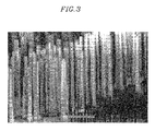
- Figure 3 is a scanning electron microscope (SEM) photograph showing ZnO having a nanorod shape. As shown in Figure 3, the ZnO nanorod has a needle structure.
- the electron amplifying materials have a high degree of shape freedom, they can be diversely patterned to form a plurality of patterns.
- FIGS. 4A to 41 are photographs showing an example of ZnO patterning with different magnifications.
- Figures 4A to 4I are pictures of the same ZnO patterning with magnifications of 2000, 8000, 180, 50,000, 600, 20,000, 18,000, 500 and 50,000, respectively.
- the electron amplifying materials are coated with at least one material selected from the group consisting of fluoride, oxide, and combinations thereof, which provides protection from oxidisation during discharge.
- the coating material may be coated with at least one material selected from the group consisting of MgO, MgF 2 , CaF 2 , LiF, Al 2 O 3 , ZnO, CaO, SrO, SiO 2 , La 2 O 3 , and combinations thereof.
- the electron amplifying material is included in a ratio ranging from 1 to 40 wt% of the entire weight of the electron amplification layer, and may be included in a ratio ranging from 5 to 30 wt%.
- a ratio ranging from 1 to 40 wt% of the entire weight of the electron amplification layer may be included in a ratio ranging from 5 to 30 wt%.
- the flat panel display device may further include at least one layer selected from the group consisting of a fluoride layer, an oxide layer, and combinations thereof, on top of the electron amplification layer.
- the flat panel display device may further include at least one layer of a protection layer 19 formed using at least one material selected from the group consisting of MgO, MgF 2 , CaF 2 , LiF, Al 2 O 3 , ZnO, CaO, SrO, SiO 2 , La 2 O 3 , and combinations thereof.
- a protection layer 19 formed using at least one material selected from the group consisting of MgO, MgF 2 , CaF 2 , LiF, Al 2 O 3 , ZnO, CaO, SrO, SiO 2 , La 2 O 3 , and combinations thereof.
- the protection layer 19 prevents the ions of separated atoms from colliding with and damaging the first dielectric layer 17, and it efficiently emits secondary electrons when the ions collide with it.
- the flat panel display device when a voltage higher than a discharge initiation voltage is applied to the space between the scan electrode and the sustain electrode disposed in parallel to each other along a direction crossing the address electrodes, the flat panel display device can emit a large number of secondary electrons when surface discharge occurs in the discharge space.
- the flat panel display device may be a plasma display panel (PDP).
- PDP plasma display panel
- the flat panel display device is manufactured by forming a plurality of display electrodes on a first substrate; forming a first dielectric layer to cover the display electrodes on the first substrate; forming an electron amplification layer by disposing an electron amplifying material selected from the group consisting of ZnO, Al 2 O 3 , SiC, diamond, and combinations thereof on the first dielectric layer; forming a plurality of address electrodes on a second substrate; forming a second dielectric layer to cover the address electrodes on the second substrate; forming a plurality of barrier ribs between the address electrodes to partition a discharge space to form a plurality of partitioned discharge spaces on the second dielectric layer; forming a phosphor layer in the partitioned discharge spaces; facing the first substrate and the second substrate to each other; exhausting air between the first substrate and the second substrate; and sealing the first substrate and the second substrate together.
- the display electrodes that are formed of a transparent electrode and a bus electrode are disposed on the first substrate, and then the first dielectric layer is disposed on the display electrodes.
- the first dielectric layer may be formed by a method known those skilled in the art, and the first dielectric layer is, in one embodiment, formed to have a thickness ranging from 10 to 20 ⁇ m.
- the electron amplification layer is formed by growing an electron amplifying material toward the discharge space on the first dielectric layer.
- the electron amplification layer may be formed by using a planting method.
- the electron amplifying material may be planted on the entire surface of the first dielectric layer, or it may be planted on the first dielectric layer in areas corresponding to the areas where the display electrodes are disposed.
- the planting process may be carried out by a method known to those skilled in the art.
- the planting is performed on the first dielectric layer by spraying the electron amplifying material or by dripping the electron amplifying material with a pipette.
- content of the electron amplifying material in the electron amplification layer may range from 1 wt% to 40 wt%.
- the content of the electron amplifying material may range from 5 wt% to 30 wt%.
- the electron amplifying material may be formed by using a material selected from the group consisting of ZnO, Al 2 O 3 , SiC, diamond (C), and combinations thereof, and may be formed of ZnO.
- At least one protection layer selected from the group consisting of a fluoride layer, an oxide layer, and combinations thereof may be additionally from on top of the electron amplification layer.
- At least one protection layer selected from the group consisting of fluoride layers including MgF 2 , CaF 2 , and LiF, and oxide layers including MgO, Al 2 O 3 , ZnO, CaO, SrO, SiO 2 , and La 2 O 3 .
- the protection layer forming method is not specifically limited. It may be formed by a thick layer printing method using a paste, or by a plasma deposition method.
- the plasma deposition method gives relatively strong against sputtering based on ion impact, and can reduce the discharge initiating voltage and the discharge sustain voltage by the emission of secondary electrons.
- Methods of forming the protection layer using the plasma deposition method include a magnetron sputtering method, an electron beam deposition method, an Ion Beam Assisted Deposition (IBAD) method, a Chemical Vapor Deposition (CVD) method, a sol-gel method, and an ion plating method.
- the ion plating method forms a layer by ionising vaporised particles.
- the ion plating method has similar characteristics to the sputtering method with respect to adherence and crystallisation of the protection layer, but it has an advantage that it can perform deposition at a high speed of 8 nm/s.
- Another suitable method for forming the protection layer is the electron beam deposition method.
- the electron amplification layer can be easily formed (without the difficulties associated with oxidising and dispersing of carbon nanotubes) to increase an electron density in the discharge space by raising a secondary electron emission coefficient of ions inside of the flat panel display device, to provide the electrons required for glow discharge, and to improve discharge characteristics and brightness characteristics by changing a discharge mode.
- Display electrodes were formed of an indium tin oxide conductive material in the shape of stripes on a first substrate that was formed of soda lime glass by using a method known to those skilled in the art.
- the entire surface of the first substrate, including the display electrodes, was coated with a dielectric paste that was formed of 28.4 wt% SiO 2 , 69.8 wt% PbO, and 1.8 wt% B 2 O 3 and baked to thereby form a first dielectric layer.
- the resultant structure was put into a protection layer deposition chamber, and a protection layer including MgO was deposited using an ion plating method to thereby complete the formation of the first substrate.
- the protection layer deposition chamber was controlled to have a regular pressure level of 1 ⁇ 10 -4 Pa and an operation pressure level of 5.3 ⁇ 10 -2 Pa during the deposition.
- the protection layer deposition chamber was further controlled to sustain the substrate at 200 ⁇ 5°C by supplying oxygen at 100 sccm.
- a plasma display panel was manufactured with substantially the same method as Example 1, except that the electron amplification layer was formed by using Al 2 O 3 nanorod.
- a plasma display panel was manufactured with substantially the same method as the Example 1, except that the electron amplification layer was not formed.
- a plasma display panel was manufactured with substantially the same method as the Example 1, except that the electron amplification layer was formed by using carbon nanotubes instead of ZnO nanorod.
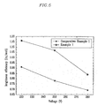
- the plasma display panel of Example 1 that included the electron amplification layer showed superior brightness characteristics to the plasma display panel of Comparative Example 1 that did not include the electron amplification layer.
- a flat panel display device of the present invention can easily form an electron amplification layer (without the difficulties associated with oxidising and dispersing of carbon nanotubes) to thereby increase an electron density by providing a sufficient amount of electrons required for high glow discharge by raising a secondary electron emission coefficient of ions inside of the flat panel display device, and improve the discharge characteristics and brightness characteristics remarkably by changing a discharge mode.
Landscapes
- Engineering & Computer Science (AREA)
- Physics & Mathematics (AREA)
- Plasma & Fusion (AREA)
- Manufacturing & Machinery (AREA)
- Gas-Filled Discharge Tubes (AREA)
Applications Claiming Priority (1)
| Application Number | Priority Date | Filing Date | Title |
|---|---|---|---|
| KR20050080645 | 2005-08-31 |
Publications (2)
| Publication Number | Publication Date |
|---|---|
| EP1760749A2 true EP1760749A2 (de) | 2007-03-07 |
| EP1760749A3 EP1760749A3 (de) | 2009-08-26 |
Family
ID=37527012
Family Applications (1)
| Application Number | Title | Priority Date | Filing Date |
|---|---|---|---|
| EP06119396A Withdrawn EP1760749A3 (de) | 2005-08-31 | 2006-08-23 | Flachbildschirmanzeige |
Country Status (2)
| Country | Link |
|---|---|
| US (1) | US20070046212A1 (de) |
| EP (1) | EP1760749A3 (de) |
Families Citing this family (2)
| Publication number | Priority date | Publication date | Assignee | Title |
|---|---|---|---|---|
| KR100696541B1 (ko) * | 2005-10-12 | 2007-03-19 | 삼성에스디아이 주식회사 | 전자방출수단을 구비한 플라즈마 디스플레이 패널 |
| US20080061698A1 (en) * | 2006-09-12 | 2008-03-13 | Matsushita Electric Industrial Co., Ltd. | Plasma display panel with intra pixel dielectric stand |
Family Cites Families (4)
| Publication number | Priority date | Publication date | Assignee | Title |
|---|---|---|---|---|
| JP2001228823A (ja) * | 1999-12-07 | 2001-08-24 | Pioneer Electronic Corp | プラズマディスプレイ装置 |
| KR100522684B1 (ko) * | 2000-11-11 | 2005-10-19 | 삼성에스디아이 주식회사 | 카본 나노 튜브층을 포함하는 전자 증폭 물질층을구비하는 평면 표시 장치 및 그 제조 방법 |
| KR20040083973A (ko) * | 2003-03-26 | 2004-10-06 | 김용석 | 보호막내 나노 팁을 포함하고 있는 고효율 플라즈마디스플레이 소자 및 그것의 제조방법 |
| US20060103307A1 (en) * | 2004-11-17 | 2006-05-18 | Matsushita Electric Industrial Co., Ltd. | Field enhanced plasma display panel |
-
2006
- 2006-08-23 EP EP06119396A patent/EP1760749A3/de not_active Withdrawn
- 2006-08-30 US US11/513,865 patent/US20070046212A1/en not_active Abandoned
Also Published As
| Publication number | Publication date |
|---|---|
| EP1760749A3 (de) | 2009-08-26 |
| US20070046212A1 (en) | 2007-03-01 |
Similar Documents
| Publication | Publication Date | Title |
|---|---|---|
| JP4532718B2 (ja) | カーボンナノチューブを採用した2次電子増幅構造体及びこれを用いたプラズマ表示パネル及びバックライト | |
| CN100559540C (zh) | 等离子显示面板及其制造方法 | |
| EP1353355B1 (de) | Plasmaanzeigegerät mit Kohlenstoff-Nanotubes und Verfahren zur Herstellung der Frontplatte des Plasmaanzeigegeräts | |
| KR100769414B1 (ko) | 전자 방출성 박막, 이를 이용한 플라즈마 디스플레이 패널및 이들의 제조 방법 | |
| KR100884152B1 (ko) | 플라즈마 디스플레이 패널 및 그 제조방법 | |
| JP4492638B2 (ja) | プラズマディスプレイパネル、プラズマディスプレイパネルの基板構体 | |
| US7956540B2 (en) | Plasma display panel | |
| EP1770748A1 (de) | Flache Anzeigetafel und Verfahren zu ihrer Herstellung | |
| US7750568B2 (en) | Plasma display panel (PDP) having a reflection preventive layer | |
| CN100370573C (zh) | 等离子显示面板和制造等离子显示面板的方法 | |
| US7446476B2 (en) | Plasma display panel | |
| US20070046212A1 (en) | Flat panel display device and manufacturing method thereof | |
| JP4102073B2 (ja) | プラズマディスプレイパネルおよびその製造方法 | |
| US20060170352A1 (en) | Plasma display panel | |
| JP4360926B2 (ja) | プラズマディスプレイパネル | |
| EP1840930B1 (de) | Plasma-Bildschirm | |
| JPH08339767A (ja) | プラズマディスプレイパネル | |
| KR100759447B1 (ko) | 평판 표시 장치 및 그 제조방법 | |
| US20070152591A1 (en) | Plasma display panel | |
| CN100424808C (zh) | 等离子体显示板 | |
| KR100759566B1 (ko) | 플라즈마 디스플레이 패널과, 이의 제조 방법 | |
| US20070216307A1 (en) | Plasma display panel | |
| KR100708848B1 (ko) | 플라즈마 디스플레이 패널 | |
| KR100708847B1 (ko) | 플라즈마 디스플레이 패널 | |
| JP2002008545A (ja) | 平面型表示装置用パネル、平面型表示装置、並びに、平面型表示装置用パネルの製造方法 |
Legal Events
| Date | Code | Title | Description |
|---|---|---|---|
| PUAI | Public reference made under article 153(3) epc to a published international application that has entered the european phase |
Free format text: ORIGINAL CODE: 0009012 |
|
| 17P | Request for examination filed |
Effective date: 20060823 |
|
| AK | Designated contracting states |
Kind code of ref document: A2 Designated state(s): AT BE BG CH CY CZ DE DK EE ES FI FR GB GR HU IE IS IT LI LT LU LV MC NL PL PT RO SE SI SK TR |
|
| AX | Request for extension of the european patent |
Extension state: AL BA HR MK YU |
|
| RAP1 | Party data changed (applicant data changed or rights of an application transferred) |
Owner name: SAMSUNG SDI CO., LTD. |
|
| PUAL | Search report despatched |
Free format text: ORIGINAL CODE: 0009013 |
|
| AK | Designated contracting states |
Kind code of ref document: A3 Designated state(s): AT BE BG CH CY CZ DE DK EE ES FI FR GB GR HU IE IS IT LI LT LU LV MC NL PL PT RO SE SI SK TR |
|
| AX | Request for extension of the european patent |
Extension state: AL BA HR MK RS |
|
| STAA | Information on the status of an ep patent application or granted ep patent |
Free format text: STATUS: THE APPLICATION HAS BEEN WITHDRAWN |
|
| 18W | Application withdrawn |
Effective date: 20091106 |