EP1758087A1 - Procede de commande d'affichage d'informations - Google Patents
Procede de commande d'affichage d'informations Download PDFInfo
- Publication number
- EP1758087A1 EP1758087A1 EP05734545A EP05734545A EP1758087A1 EP 1758087 A1 EP1758087 A1 EP 1758087A1 EP 05734545 A EP05734545 A EP 05734545A EP 05734545 A EP05734545 A EP 05734545A EP 1758087 A1 EP1758087 A1 EP 1758087A1
- Authority
- EP
- European Patent Office
- Prior art keywords
- voltage
- driving
- color
- display
- talk
- Prior art date
- Legal status (The legal status is an assumption and is not a legal conclusion. Google has not performed a legal analysis and makes no representation as to the accuracy of the status listed.)
- Ceased
Links
Images


Classifications
-
- G—PHYSICS
- G09—EDUCATION; CRYPTOGRAPHY; DISPLAY; ADVERTISING; SEALS
- G09G—ARRANGEMENTS OR CIRCUITS FOR CONTROL OF INDICATING DEVICES USING STATIC MEANS TO PRESENT VARIABLE INFORMATION
- G09G3/00—Control arrangements or circuits, of interest only in connection with visual indicators other than cathode-ray tubes
- G09G3/20—Control arrangements or circuits, of interest only in connection with visual indicators other than cathode-ray tubes for presentation of an assembly of a number of characters, e.g. a page, by composing the assembly by combination of individual elements arranged in a matrix no fixed position being assigned to or needed to be assigned to the individual characters or partial characters
- G09G3/34—Control arrangements or circuits, of interest only in connection with visual indicators other than cathode-ray tubes for presentation of an assembly of a number of characters, e.g. a page, by composing the assembly by combination of individual elements arranged in a matrix no fixed position being assigned to or needed to be assigned to the individual characters or partial characters by control of light from an independent source
- G09G3/3433—Control arrangements or circuits, of interest only in connection with visual indicators other than cathode-ray tubes for presentation of an assembly of a number of characters, e.g. a page, by composing the assembly by combination of individual elements arranged in a matrix no fixed position being assigned to or needed to be assigned to the individual characters or partial characters by control of light from an independent source using light modulating elements actuated by an electric field and being other than liquid crystal devices and electrochromic devices
- G09G3/344—Control arrangements or circuits, of interest only in connection with visual indicators other than cathode-ray tubes for presentation of an assembly of a number of characters, e.g. a page, by composing the assembly by combination of individual elements arranged in a matrix no fixed position being assigned to or needed to be assigned to the individual characters or partial characters by control of light from an independent source using light modulating elements actuated by an electric field and being other than liquid crystal devices and electrochromic devices based on particles moving in a fluid or in a gas, e.g. electrophoretic devices
-
- G—PHYSICS
- G09—EDUCATION; CRYPTOGRAPHY; DISPLAY; ADVERTISING; SEALS
- G09G—ARRANGEMENTS OR CIRCUITS FOR CONTROL OF INDICATING DEVICES USING STATIC MEANS TO PRESENT VARIABLE INFORMATION
- G09G2300/00—Aspects of the constitution of display devices
- G09G2300/06—Passive matrix structure, i.e. with direct application of both column and row voltages to the light emitting or modulating elements, other than LCD or OLED
-
- G—PHYSICS
- G09—EDUCATION; CRYPTOGRAPHY; DISPLAY; ADVERTISING; SEALS
- G09G—ARRANGEMENTS OR CIRCUITS FOR CONTROL OF INDICATING DEVICES USING STATIC MEANS TO PRESENT VARIABLE INFORMATION
- G09G2310/00—Command of the display device
- G09G2310/06—Details of flat display driving waveforms
-
- G—PHYSICS
- G09—EDUCATION; CRYPTOGRAPHY; DISPLAY; ADVERTISING; SEALS
- G09G—ARRANGEMENTS OR CIRCUITS FOR CONTROL OF INDICATING DEVICES USING STATIC MEANS TO PRESENT VARIABLE INFORMATION
- G09G2310/00—Command of the display device
- G09G2310/06—Details of flat display driving waveforms
- G09G2310/061—Details of flat display driving waveforms for resetting or blanking
-
- G—PHYSICS
- G09—EDUCATION; CRYPTOGRAPHY; DISPLAY; ADVERTISING; SEALS
- G09G—ARRANGEMENTS OR CIRCUITS FOR CONTROL OF INDICATING DEVICES USING STATIC MEANS TO PRESENT VARIABLE INFORMATION
- G09G2320/00—Control of display operating conditions
- G09G2320/02—Improving the quality of display appearance
- G09G2320/0209—Crosstalk reduction, i.e. to reduce direct or indirect influences of signals directed to a certain pixel of the displayed image on other pixels of said image, inclusive of influences affecting pixels in different frames or fields or sub-images which constitute a same image, e.g. left and right images of a stereoscopic display
-
- G—PHYSICS
- G09—EDUCATION; CRYPTOGRAPHY; DISPLAY; ADVERTISING; SEALS
- G09G—ARRANGEMENTS OR CIRCUITS FOR CONTROL OF INDICATING DEVICES USING STATIC MEANS TO PRESENT VARIABLE INFORMATION
- G09G2320/00—Control of display operating conditions
- G09G2320/02—Improving the quality of display appearance
- G09G2320/0233—Improving the luminance or brightness uniformity across the screen
-
- G—PHYSICS
- G09—EDUCATION; CRYPTOGRAPHY; DISPLAY; ADVERTISING; SEALS
- G09G—ARRANGEMENTS OR CIRCUITS FOR CONTROL OF INDICATING DEVICES USING STATIC MEANS TO PRESENT VARIABLE INFORMATION
- G09G3/00—Control arrangements or circuits, of interest only in connection with visual indicators other than cathode-ray tubes
- G09G3/20—Control arrangements or circuits, of interest only in connection with visual indicators other than cathode-ray tubes for presentation of an assembly of a number of characters, e.g. a page, by composing the assembly by combination of individual elements arranged in a matrix no fixed position being assigned to or needed to be assigned to the individual characters or partial characters
- G09G3/2007—Display of intermediate tones
- G09G3/2018—Display of intermediate tones by time modulation using two or more time intervals
Definitions
- the present invention relates to a method of driving an information display device, in which two groups of display media having at least first color and second color are sealed between opposed two substrates, at least one substrate being transparent, and, in which the display media, to which an electrostatic field is applied from the electrodes, are made to move so as to display information such as an image (first aspect and second aspect of the invention). Moreover, the present invention relates to a method of driving an information display device, in which display media are sealed between opposed two substrates, at least one substrate being transparent, and, in which the display media, to which an electrostatic field is applied from electrodes, are made to move so as to display information such as an image (third aspect of the invention).
- information display devices substitutable for liquid crystal display (LCD)
- information display devices with the use of technology such as an electrophoresis method, an electro-chromic method, a thermal method, dichroic-particles-rotary method are proposed.
- an information display device comprising an information display panel
- the display media particles or liquid powders
- the display media are sealed between a front substrate having a front electrode and a rear substrate having a rear electrode
- the display media, to which an electrostatic field is applied are made to move by means of Coulomb's force and so on so as to display information such as an image.
- the cross-talk is basically a phenomenon such that one line is mixed with the other line on the phone.
- the cross-talk is a phenomenon such that, even if the column electrode is not selected, an image other than actual one is displayed due to the other lines.
- a voltage is applied to a non-selected line of the column electrodes so as to maintain the image. Since the maintaining voltage is applied only to the number of the lines of the column electrodes, a contrast becomes worse, and a shading of an image display is generated according to a display pattern, so that the image is lacking in color uniformity.
- the cross-talk is basically a phenomenon such that one line is mixed with the other line on the phone.
- the cross-talk is a phenomenon such that, even if the column electrode is not selected, an image other than actual one is displayed due to the other lines.
- a voltage is applied to a non-selected line of the column electrodes so as to maintain the image. Since the maintaining voltage is applied only to the number of the lines of the column electrodes, a shading of an image display is generated, and the image is lacking in color uniformity.
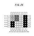
- Fig. 25 is a schematic view showing a shading non-uniformity due to the cross-talk in the known image display device.
- 8 x 6 image consisting of line electrodes 51-1 to 51-6 at a lower side and column electrodes 52-1 to 52-8 at an upper side is shown.
- the display media having a white color and a black color and having different characteristics with each other are filled between the line electrodes and the column electrodes, and a white & black color display is performed in response to a voltage applied between the line electrodes 51-1 to 51-6 and the column electrodes 52-1 to 52-8.
- a driving method use is made of a line deleting method in which a deleting operation and a writing operation are repeated on every line, and a scanning operation is performed to the line electrodes 51-1 to 51-6 in this order so as to display an image.
- a scanning operation is performed, a deleting operation for the selected line of the line electrodes 51-1 to 51-6 is performed by applying a voltage 100 and its writing operation is performed by applying a voltage 0.
- a deleting operation for the non-selected lie is performed by applying a voltage 50.
- a deleting operation for the column electrodes 52-1 to 52-8 is performed by applying a voltage 0, and its writing operation for a writing column is performed by applying a voltage 100, while applying a voltage 0 to the column other than the writing column.
- the scanning operation starts from the first line elctrode51-1 and is finished at the last line electrode 51-6.
- a portion at which a white color should be displayed is displayed as a white gray color
- a portion at which a black color should be displayed is displayed as a black gray color, so that a shading of an image display is generated and the image is lacking in color uniformity.
- the cross-talk is basically a phenomenon such that one line is mixed with the other line on the phone.
- the cross-talk is a phenomenon such that, even if the column electrode is not selected, an image other than actual one is displayed due to the other lines.
- a voltage is applied to a non-selected line of the column electrodes so as to maintain the image. Since the maintaining voltage is applied only to the number of the lines of the column electrodes, a shading of an image display is generated, and the image is lacking in color uniformity.
- An object of a first aspect of the invention is to eliminate the drawbacks mentioned above and to provide a method of driving an information display device, which can remove a color non-uniformity of the image due to the cross-talk.
- a method of driving an information display device in which two groups of display media having at least first color and second color are sealed between opposed two substrates, at least one substrate being transparent, and, in which the display media, to which an electrostatic field is applied from electrodes arranged respectively to the substrates, are made to move so as to display information such as an image, is characterized in that, when information of one frame such as an image is displayed by performing a scanning operation with respect to line electrodes consisting of a plurality of electrodes extending in a line direction on one substrate and column electrodes consisting of a plurality electrodes extending in a column direction on the other substrate in such a manner that a voltage is applied to the line electrodes from one end to the other end, a voltage for generating a cross-talk in the first color and a voltage for generating a cross-talk in the second color are applied to all the cells of a display portion once or more times respectively after one frame is displayed.
- the method of driving the information display device there are cases: such that two or more lines are added at the end of the scanning operation, and a drive, in which a display of the first color and a display of the second color are performed one or more times respectively, is performed after one scanning operation is finished; and such that a deleting operation of the image prior to the image display is performed by a line deleting method in which the image is written one by one for the lines after the lines are deleted respectively, or, by a full deleting method in which the image is written one by one for the lines after all the lines are deleted at the same time.
- a voltage for generating a cross-talk in the first color and a voltage for generating a cross-talk in the second color are applied to all the cells of a display portion once or more times respectively after one frame is displayed; or preferably since two or more lines are added at the end of the scanning operation, and a drive, in which a display of the first color and a display of the second color are performed one or more times respectively, is performed after one scanning operation is finished; when a white color & black color display is performed for example, a white color can be displayed as a slightly black pale gray, and a black color can be displayed as a slightly white dark gray, so that it is possible to prevent a color non-uniformity of the image due to the cross-talk.
- An object of a second aspect of the invention is to eliminate the drawbacks mentioned above and to provide a method of driving an information display device, which can remove a color non-uniformity of the image and a decrease of contrast due to the cross-talk.
- q method of driving an information display device in which two groups of display media having at least first color and second color are sealed between opposed two substrates, at least one substrate being transparent, and, in which the display media, to which an electrostatic field is applied from the electrodes, are made to move so as to display information such as an image
- a driving voltage applied to the electrodes for generating an electrostatic field use is made of a pulse voltage which is composed of a plurality of voltages consisting of a driving voltage generating an ON state and a voltage of not larger than a threshold value, at which the display media start to move, generating an OFF state.
- a driving voltage V is larger than a threshold voltage V 1 (V > V 1 > V 0 : V 0 means a voltage lower than the threshold value).
- a driving voltage applied to the electrodes for generating an electrostatic field use is made of a pulse voltage which is composed of a plurality of voltages consisting of a driving voltage generating an ON state and a voltage of not larger than a threshold value, at which the display media start to move, generating an OFF state, it is possible to remove a color non-uniformity of the image and a decrease of contrast due to the cross-talk.
- An object of a third aspect of the invention is to eliminate the drawbacks mentioned above and to provide a method of driving an information display device, which can remove a decrease of contrast due to the cross-talk voltage.
- a method of driving an information display device in which display media are sealed between opposed two substrates, at least one substrate being transparent, and, in which the display media, to which an electrostatic field is applied from electrodes, are made to move so as to display information such as an image, is characterized in that, when a pixel rewriting operation is performed once, a plurality of pulses are applied, and, during the one pixel rewriting operation, a driving waveform is adjusted in such a manner that a polarity of a cross-talk voltage applied to a non-rewriting pixel is not changed.
- an electrostatic field is applied to the particles sealed between opposed two substrates.
- Charged particles are attracted along a direction of electrostatic field to be applied by means of Coulomb's force in such a manner that the particles charged at a low potential are attracted toward a high potential side and the particles charged at a high potential are attracted toward a low potential side, and thus the particles can be moved reciprocally by varying a direction of electrostatic field due to a switching operation of potential. Accordingly, an image can be displayed.
- the information display panel in such a manner that the display media can move evenly and maintain stability during a reciprocal operation or during a reserving state.
- forces applied to the particles there are an attraction force between the particles due to Coulomb' force, an imaging force with respect to the electrode panel, an intermolecular force, a liquid bonding force and a gravity.
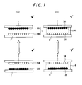
- At least two or more groups of display media 3 having different optical reflectance and different charge characteristics and consisting of at least one or more groups of particles are moved in a perpendicular direction with respect to substrates 1 and 2, in accordance with an electric field generated by applying a voltage between electrodes (not shown) arranged outside of the substrates 1 and 2, so as to display a black color by viewing the black color display media 3B to an observer or so as to display a white color by viewing the white color display media 3W to the observer.
- a cell is formed by arranging for example grid-like partition walls 4 between the substrates 1 and 2, in addition to the example shown in Fig. 1a.
- the partition walls arranged at the near side are omitted.
- a white color display media 3W made of the particles and a black color display media 3B made of the particles are shown
- a white color display media 3W made of the particles and a black color display media 3B made of the particles are shown
- a cell is formed by arranging for example grid-like partition walls 4 between the substrates 1 and 2, in addition to the example shown in Fig. 2a.
- the partition walls arranged at the near side are omitted.
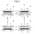
- At least one group of display media 3 having one color and one charge characteristic and consisting of at least one or more groups of particles are moved in a parallel direction with respect to substrates 1 and 2, in accordance with an electric field generated by applying a voltage between the electrode 5 arranged to the substrate 1 and the electrode 6 arranged to the substrate 1, so as to display a white color by viewing the white color display media 3W to an observer or so as to display a color of the electrode 6 or the substrate 1 by viewing a color of the electrode 6 or the substrate 1 to the observer.
- a cell is formed by arranging for example grid-like partition walls 4 between the substrates 1 and 2, in addition to the example shown in Fig. 3a.
- the partition walls arranged at the near side are omitted.
- the cross-talk voltages 1 and 2 when a voltage 100 and a voltage -100 are applied so as to display a white color as a first color and a black color as a second color, a voltage 50 is applied as the cross-talk voltage 1 and a voltage -50 is applied as the cross-talk voltage 2.
- a voltage 50 is applied as the cross-talk voltage 1
- a voltage -50 is applied as the cross-talk voltage 2.
- a drive in which a display of the first color and a display of the second color are performed one or more times respectively, is performed after one scanning operation is finished.
- Figs. 4a, 4b and Figs. 5a, 5b are schematic views respectively explaining one embodiment in which a driving method according to the invention is incorporated into the known one shown in Fig. 25.
- line electrodes 11-7, 11-8 are previously added to line electrodes 11-1 to 11-6 and column electrodes 12-1 to 12-8 as is the same as the known one shown in Fig. 25.
- a scanning operation for an image display portion i.e., after one frame of information such as an image consisting of 8 x 6 pixels is displayed by performing a scanning operation till the line electrode 11-6, with respect to a first line electrode 11-7 in the last two lines
- a deleting operation is performed as shown in Fig. 4a and then a writing operation of a white color is performed as shown in Fig. 4b.
- a deleting operation is performed as shown in Fig. 5a and then a writing operation of a black color is performed as shown in Fig. 5b.
- the white color is integrated as a pale gray and the black color is integrated as a dark gray.
- 100 % white color and 100 % black color cannot be obtained, but all the portions to be displayed in a white color are displayed in a pale gray and all the portions to be displayed in a black color are displayed in a dark gray. Therefore, it is possible to completely eliminate a shading non-uniformity due to the cross-talk.
- the line electrodes 11-7 and 11-8 are actually added so as to display a white & black color by means of the display media.
- the electrodes are not arranged, and, two or more driving lines are added, to which a voltage for performing a white color display and a voltage for performing a black color display are applied, it is possible to eliminate a shading non-uniformity in the same manner.
- the first color for example white color
- the second color for example black color
- Figs. 6a and 6b are schematic views respectively explaining another embodiment of the method of driving the information display device according to the first aspect of the invention.
- a checker pattern is displayed on the line electrode 11-7 and 11-8, a shading non-uniformity can be eliminated, as is the same as the embodiments shown in Figs. 4a, 4b and Figs. 5a, 5b.
- the checker pattern display can be performed in the following manner. That is, when the first color display and the second color display are performed with respect to respective columns in the last two lines, a zigzag display, in which an order of the first color display and the second color display is different on respective columns, is performed.
- a zig-zag display in which a voltage is applied in such a manner that an order of the first color display and the second color display is different on respective columns, is performed.
- Fig. 7, Figs. 8a, 8b and Figs. 9a, 9b are schematic views respectively explaining the information display device according to the first aspect of the invention.
- a pattern image shown in Fig. 7 is displayed.
- Fig. 8a an example, in which the pattern image is displayed by the line deleting method according to the known driving method, is shown in Fig. 8a, and an example, in which the pattern image is displayed by the line deleting method according to the driving method of the present invention such that the white color and the black color are written in the last two lines, is shown in Fig. 8b.
- Fig. 9a an example, in which the pattern image is displayed by the full deleting method according to the known driving method, is shown in Fig. 9a
- Fig. 9b an example, in which the pattern image is displayed by the full deleting method according to the driving method of the present invention such that the white color and the black color are written in the last two lines, is shown in Fig. 9b.
- Figs. 8a and 8b both in the line deleting method and the full deleting method
- an image shading due to the cross-talk is remarkably detected in the known examples, but no image shading due to the cross-talk is detected in the examples according to the invention.
- the voltage 100 applied when the pixel is deleted and written is not explained, but image shading is largely different by a voltage V in response to the structure of the image display device.
- a voltage V in response to the structure of the image display device.
- the voltage V is low, a black color display is not performed.
- the voltage V is high, there is no difference between a gray portion due to the cross-talk and a black portion. Therefore, according to the structure of the image display device, it is necessary to select most suitable voltage.
- a feature of the method of driving the information display device is that, in the image display device having the construction mentioned above, use is made of a pulse voltage which is composed of a plurality of voltages consisting of a driving voltage V generating an ON state and a voltage V 0 of not larger than a threshold value, at which the display media start to move, generating an OFF state, while, in the known driving method, the driving voltage V generating an ON state is continuously applied so as to display an image.
- a new concept such as a period of OFF state (OFF period), in which the voltage V 0 of not larger than a threshold value, is used so that the cross-talk is reduced by controlling the OFF period.
- V 0 and V may be composed of a plurality of voltage levels respectively and they may be varied gradually.
- Fig. 10 is a schematic view showing one embodiment of a pulse voltage used for the method of driving the information display device according to the second aspect of the invention.
- the pulse voltage used in the present invention is composed of the driving voltage generating the ON state and the voltage of not larger than a threshold value (V 1 ), at which the display media start to move, generating the OFF state.
- V 1 a threshold value
- there are cases: such that a duty ratio ( pulse width / (pulse width + period of the OFF state)) of the pulse voltage is not larger than 0.9; and such that a period of the OFF state is not less than 0.1 msec. Both embodiments will be explained in detail in the examples mentioned below.
- a feature of the method of driving the image display device is that, in the image display device having the construction mentioned above, a cross-talk voltage waveform is further investigated in detail in the case of applying various driving methods, and the most suitable method is selected, so that a contrast is improved. Specifically, when a pixel rewriting operation is performed once, a plurality of pulses are applied, and, a pulse waveform of the driving voltage is controlled in such a manner that a polarity of a cross-talk voltage applied to a non-rewriting pixel is not changed, i.e.
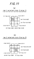
- Figs. 11a and 11b are schematic views respectively showing a row 1 selected state and a row 2 selected state in a passive matrix of 2 rows and 2 columns.
- a rewriting voltage is applied to a pixel to be rewrote (hatched area in the figure)
- three kinds of cross-talk voltages such as cross-talk -1 to -3 shown in the figure are applied. If the number of rows is increased, there are only two kinds of voltages mentioned above (two kinds of row selected state and row non-selected state, two kinds of column rewriting state and column non-rewriting state, thus two kinds in 2 ⁇ 2). If use is made of more complex driving logic, further more kinds of voltages exist).
- a display color of the rewriting pixel can be made black in addition to the contrast improvement mentioned above by widening a peak-to-peak distance of the pulse voltages applied to the rewriting pixel, during the period for which a plurality of pulses are applied when the pixel rewriting operation is performed once, so that a contrast can be further improved.
- a row (scan) driving voltage and a column driving voltage are composed of a pulse train with same cycle and same duty, and, when the pulse train at a row side is selected, a phase of the pulse train of the row driving voltage and the column driving voltage is inverted respectively.
- a difference of peak-to-peak can be made larger in the cross-talk voltage applied as a difference between the row (scan) driving voltage and the column driving voltage to the rewriting pixel, so that a color of the rewriting pixel can be made dark.
- the substrate As the substrate, at least one of the substrates is the transparent front substrate 2 through which a color of the particles or the liquid powders can be observed from outside of the device, and it is preferred to use a material having a high transmission factor of visible light and an excellent heat resistance.
- the rear substrate 1 may be transparent or may be opaque.
- the substrate material include polymer sheets such as polyethylene terephthalate, polyether sulfone, polyethylene, polycarbonate, polyimide or acryl and metal sheets having flexibility and inorganic sheets such as glass, quartz or so having no flexibility.
- the thickness of the substrate is preferably 2 to 5000 ⁇ m, more preferably 5 to 2000 ⁇ m. When the thickness is too thin, it becomes difficult to maintain strength and distance uniformity between the substrates, and when the thickness is thicker than 5000 ⁇ m, there is a drawback as a thin-type information display panel.
- the electrode As a material of the electrode in the case of arranging the electrode on the information display panel, use is made of metals such as aluminum, silver, nickel, copper, gold, or, conductive metal oxides such as ITO, indium oxide, conductive tin oxide, conductive zinc oxide and so on, or, conductive polymers such as polyaniline, polypyrrole, polythiophene and so on, and they are used by being suitably selected.
- metals such as aluminum, silver, nickel, copper, gold, or, conductive metal oxides such as ITO, indium oxide, conductive tin oxide, conductive zinc oxide and so on, or, conductive polymers such as polyaniline, polypyrrole, polythiophene and so on, and they are used by being suitably selected.
- an electrode forming method use is made of a method in which the materials mentioned above are made to a thin film by means of sputtering method, vacuum vapor deposition method, CVD (chemical vapor deposition) method, coating method and so on, or, a method in which conductive materials and solvents are mixed with synthetic resin binder and the mixture is sprayed.
- a transparency is necessary for the electrode arranged to the substrate at an observation side (display surface side), but it is not necessary to the substrate at a rear side. In both cases, the materials mentioned above, which are transparent and have a pattern formation capability, can be suitably used.
- the thickness of the electrode may be suitable unless the electro-conductivity is absent or any hindrance exists in optical transparency, and it is preferable to be 3 to 1000 nm, more preferable to be 5 to 400 nm.
- the material and the thickness of the electrode arranged to the rear substrate are the same as those of the electrode arranged to the substrate at the display side, but transparency is not necessary. In this case, the applied outer voltage may be superimposed with a direct current or an alternate current.
- a shape of the partition wall is suitably designed in accordance with a kind of the display media used for the display and is not restricted. However, it is preferred to set a width of the partition wall to 2 - 100 ⁇ m more preferably 3 - 50 ⁇ m and to set a height of the partition wall to 10 - 500 ⁇ m more preferably 10 - 200 ⁇ m.
- a method of forming the partition wall use may be made of a double rib method wherein ribs are formed on the opposed substrates respectively and they are connected with each other and a single rib method wherein a rib is formed on one of the opposed substrates only.
- the present invention may be preferably applied to both methods mentioned above.
- the cell formed by the partition walls each made of rib has a square shape, a triangular shape, a line shape, a circular shape and a hexagon shape, and has an arrangement such as a grid, a honeycomb and a mesh, as shown in Fig. 12 viewed from a plane surface of the substrate. It is preferred that the portion corresponding to a cross section of the partition wall observed from the display side (an area of the frame portion of the cell) should be made as small as possible. In this case, a clearness of the image display can be improved.
- the formation method of the partition wall is not particularly restricted, however, a die transfer method, a screen-printing method, a sandblast method, a photolithography method and an additive method. Among them, it is preferred to use a photolithography method using a resist film or a die transfer method.
- the particle constituting the particles may be composed of resins as a main ingredient, and can include according to need charge control agents, coloring agent, inorganic additives and so on as is the same as the known one.
- charge control agents coloring agent, inorganic additives and so on as is the same as the known one.
- typical examples of resin, charge control agent, coloring agent, additive and so on will be explained.
- the resin include urethane resin, urea resin, acrylic resin, polyester resin, acryl urethane resin, acryl urethane silicone resin, acryl urethane fluorocarbon polymers, acryl fluorocarbon polymers, silicone resin, acryl silicone resin, epoxy resin, polystyrene resin, styrene acrylic resin, polyolefin resin, butyral resin, vinylidene chloride resin, melamine resin, phenolic resin, fluorocarbon polymers, polycarbonate resin, polysulfon resin, polyether resin, and polyamide resin. Two kinds or more of these may be mixed and used.
- acryl urethane resin for the purpose of controlling the attaching force with the substrate, acryl urethane resin, acryl silicone resin, acryl fluorocarbon polymers, acryl urethane silicone resin, acryl urethane fluorocarbon polymers, fluorocarbon polymers, silicone resin are particularly preferable.
- Examples of the electric charge control agent include, but not particularly specified to, negative charge control agent such as salicylic acid metal complex, metal containing azo dye, oil-soluble dye of metal-containing (containing a metal ion or a metal atom), the fourth grade ammonium salt-based compound, calixarene compound, boron-containing compound (benzyl acid boron complex), and nitroimidazole derivative.
- negative charge control agent such as salicylic acid metal complex, metal containing azo dye, oil-soluble dye of metal-containing (containing a metal ion or a metal atom), the fourth grade ammonium salt-based compound, calixarene compound, boron-containing compound (benzyl acid boron complex), and nitroimidazole derivative.
- Examples of the positive charge control agent include nigrosine dye, triphenylmethane compound, the fourth grade ammonium salt compound, polyamine resin, imidazole derivatives, etc.
- metal oxides such as ultra-fine particles of silica, ultra-fine particles of titanium oxide, ultra-fine particles of alumina, and so on; nitrogen-containing circular compound such as pyridine, and so on, and these derivates or salts; and resins containing various organic pigments, fluorine, chlorine, nitrogen, etc. can be employed as the electric charge control agent.
- coloring agent various kinds and colors of organic or inorganic pigments or dye as will be described below are employable.
- black pigments include carbon black, copper oxide, manganese dioxide, aniline black, and activate carbon.
- blue pigments include C.I. pigment blue 15:3, C.I. pigment blue 15, Berlin blue, cobalt blue, alkali blue lake, Victoria blue lake, phthalocyanine blue, metal-free phthalocyanine blue, partially chlorinated phthalocyanine blue, first sky blue, and Indanthrene blue BC.
- red pigments examples include red oxide, cadmium red, diachylon, mercury sulfide, cadmium, permanent red 4R, lithol red, pyrazolone red, watching red, calcium salt, lake red D, brilliant carmine 6B, eosin lake, rhodamine lake B, alizarin lake, brilliant carmine 3B, and C.I. pigment red 2.
- yellow pigments include chrome yellow, zinc chromate, cadmium yellow, yellow iron oxide, mineral first yellow, nickel titanium yellow, navel orange yellow, naphthol yellow S, hansayellow G, hansayellow 10G, benzidine yellow G, benzidine yellow GR, quinoline yellow lake, permanent yellow NCG, tartrazinelake, and C.I. pigment yellow 12.
- green pigments include chrome green, chromium oxide, pigment green B, C.I. pigment green 7,Malachite green lake, and final yellow green G.
- orange pigments examples include red chrome yellow, molybdenum orange, permanent orange GTR, pyrazolone orange, Balkan orange, Indanthrene brilliant orange RK, benzidine orange G, Indanthrene brilliant orange GK, and C.I. pigment orange 31.
- purple pigments include manganese purple, first violet B, and methyl violet lake.
- white pigments include zinc white, titanium oxide, antimony white, and zinc sulphide.
- extenders examples include baryta powder, barium carbonate, clay, silica, white carbon, talc, and alumina white. Furthermore, there are Nigrosine, Methylene Blue, rose bengal, quinoline yellow, and ultramarine blue as various dyes such as basic dye, acidic dye, dispersion dye, direct dye, etc.
- inorganic additives include titanium oxide, zinc white, zinc sulphide, antimony oxide, calcium carbonate, pearl white, talc, silica, calcium silicate, alumina white, cadmium yellow, cadmium red, titanium yellow, Pressian blue, Armenian blue, cobalt blue, cobalt green, cobalt violet, ion oxide, carbon black, manganese ferrite black, cobalt ferrite black, copper powder, aluminum powder.
- These coloring agents and inorganic additives may be used alone or in combination of two or more kinds thereof. Particularly, carbon black is preferable as the black coloring agent, and titanium oxide is preferable as the white coloring agent.
- the average particle diameter d(0.5) of the particles to be used it is preferred to set d(0.5) to 0.1 - 20 ⁇ m and to use even particles. If the average particle diameter d(0.5) exceeds this range, the image clearness sometimes deteriorated, and, if the average particle diameter is smaller than this range, an agglutination force between the particles becomes too large and the movement of the particles is prevented.
- a ratio of d(0.5) of the particles having smallest diameter with respect to d(0.5) of the particles having largest diameter is set to not more than 50 preferably not more than 10.
- the particles having different charge characteristics with each other are moved reversely, even if the particle diameter distribution Span is made smaller. Therefore, it is preferred that the particle sizes of the particles are made to be even with each other, and same amounts of the particles are easily moved in a reverse direction, and thus that is this range.
- the particle diameter distribution and the particle diameter mentioned above can be measured by means of a laser diffraction / scattering method.
- a laser light is incident upon the particles to be measured, a light intensity distribution pattern due to a diffraction / scattering light occurs spatially.
- This light intensity distribution pattern corresponds to the particle diameter, and thus it is possible to measure the particle diameter and the particle diameter distribution.
- the particle diameter and the particle diameter distribution are obtained by a volume standard distribution.
- the particle diameter and the particle diameter distribution can be measured by means of a measuring apparatus Mastersizer 2000 (Malvern Instruments Ltd.) wherein the particles setting in a nitrogen gas flow are calculated by an installed analysis software (which is based on a volume standard distribution due to Mie's theory).
- a charge amount of the display media properly depends upon the measuring condition.
- the charge amount of the display media used for the display media in the information display panel substantially depends upon an initial charge amount, a contact with respect to the partition wall, a contact with respect to the substrate, a charge decay due to an elapsed time, and specifically a saturation value of the particles for the display media during a charge behavior is a main factor.
- liquid powders including at least the white color particles according to the invention will be explained. It should be noted that a right of the name of liquid powders used in the information display panel according to the invention is granted to the applicant as "liquid powders" (Registered): register No. 4636931.
- liquid powders means an intermediate material having both of liquid properties and particle properties and exhibiting a self-fluidity without utilizing gas force and liquid force.
- it is a material having an excellent fluidity such that there is no repose angle defining a fluidity of powder.
- a liquid crystal is defined as an intermediate phase between a liquid and a solid, and has a fluidity showing a liquid characteristic and an anisotropy (optical property) showing a solid characteristic (Heibonsha Ltd.: encyclopedia).
- a definition of the particle is a material having a finite mass if it is vanishingly small and receives an attraction of gravity (Maruzen Co., Ltd.: physics subject-book).
- gas-solid fluidized body If a gas is flown from a bottom plate to the particles, an upper force is acted with respect to the particles in response to a gas speed.
- the gas-solid fluidized body means a state that is easily fluidized when the upper force is balanced with the gravity.
- the liquid-solid fluidized body means a state that is fluidized by a liquid.
- the intermediate material having both of fluid properties and solid properties and exhibiting a self-fluidity without utilizing gas force and liquid force can be produced specifically, and this is defined as the liquid powders.
- the liquid powders according to the invention are a material showing the intermediate state having both of liquid properties and particle properties, which is extremely difficult to receive an influence of the gravity showing the particle properties mentioned above and indicates a high fluidity.
- a material can be obtained in an aerosol state i.e. in a dispersion system wherein a solid-like or a liquid-like material is floating in a relatively stable manner as a dispersant in a gas, and thus, in the information display panel according to the invention, a solid material is used as a dispersant.
- the information display panel which is a target of the present invention has a construction such that the liquid powders composed of a solid material stably floating as a dispersoid in a gas and exhibiting a high fluidity in an aerosol state are sealed between opposed two substrates, wherein one of two substrates is transparent.
- Such liquid powders can be made to move easily and stably by means of Coulomb's force and so on generated by applying a low voltage.
- the liquid powders means an intermediate material having both of liquid properties and particle properties and exhibiting a self-fluidity without utilizing gas force and liquid force. Such liquid powders become particularly an aerosol state.
- the liquid powders used in a state such that a solid material is relatively and stably floating as a dispersoid in a gas.
- an apparent volume in a maximum floating state is two times or more than that in none floating state, more preferably 2.5 times or more than that in none floating state, and most preferably three times or more than that in none floating state.
- an upper limit is not defined, but it is preferred that an apparent volume is 12 times or smaller than that in none floating state. If the apparent volume in the maximum floating state is smaller than two times, a display controlling becomes difficult. On the other hand, if the apparent volume in the maximum floating state is larger than 12 times, a handling inconvenience during a liquid powders filling operation into the device such as a particle over-scattering occurs.
- the liquid powders having a volume 1/5 of the vessel are filled as the liquid powders in a polypropylene vessel with a cap having a diameter (inner diameter) of 6 cm and a height of 10 cm (product name I-boy produced by As-one Co., Ltd.), the vessel is set in the vibrator, and a vibration wherein a distance of 6 cm is repeated at a speed of 3 reciprocating/sec. is performed for 3 hours. Then, the apparent volume in the maximum floating state is obtained from an apparent volume just after a vibration stop.
- a time change of the apparent volume of the liquid powders satisfies the following formula: V 10 / V 5 > 0.8 ; here, V 5 indicates the apparent volume (cm 3 ) of the liquid powders after 5 minutes from the maximum floating state; and V 10 indicates the apparent volume (cm 3 ) of the liquid powders after 10 minutes from the maximum floating state.
- V 10 indicates the apparent volume (cm 3 ) of the liquid powders after 10 minutes from the maximum floating state.
- the average particle diameter d(0.5) of the particle materials constituting the liquid powders is 0.1 - 20 ⁇ m, more preferably 0.5 - 15 ⁇ m, most preferably 0.9 - 8 ⁇ m. If the average particle diameter d(0.5) is less than 0.1 ⁇ m, a display controlling becomes difficult. On the other hand, if the average particle diameter d(0.5) is larger than 20 ⁇ m, a display clearness becomes deteriorated.
- the average particle diameter d(0.5) of the particle materials constituting the liquid powders is equal to d(0.5) in the following particle diameter distribution Span.
- the particle diameter distribution and the particle diameter mentioned above can be measured by means of a laser diffraction / scattering method.
- a laser light is incident upon the particles to be measured, a light intensity distribution pattern due to a diffraction / scattering light occurs spatially.
- This light intensity distribution pattern corresponds to the particle diameter, and thus it is possible to measure the particle diameter and the particle diameter distribution.
- the particle diameter and the particle diameter distribution are obtained by a volume standard distribution.
- the particle diameter and the particle diameter distribution can be measured by means of a measuring apparatus Mastersizer 2000 (Malvern Instruments Ltd.) wherein the particles setting in a nitrogen gas flow are calculated by an installed analysis software (which is based on a volume standard distribution due to Mie's theory).
- the liquid powders may be formed by mixing necessary resin, charge control agent, coloring agent, additive and so on and crushing them, or, by polymerizing from monomer, or, by coating a particle with resin, charge control agent, coloring agent, and additive and so on.
- resin, charge control agent, coloring agent, additive and so on constituting the liquid powders will be explained.
- Typical examples of the resin include urethane resin, acrylic resin, polyester resin, modified acryl urethane resin, silicone resin, nylon resin, epoxy resin, styrene resin, butyral resin, vinylidene chloride resin, melamine resin, phenolic resin, fluorocarbon polymers, and it is possible to combine two or more resins.
- acryl urethane resin, acryl urethane silicone resin, acryl urethane fluorocarbon polymers, urethane resin, fluorocarbon polymers are preferred.
- charge control agent examples include, positive charge control agent including the fourth grade ammonium salt compound, nigrosine dye, triphenylmethane compound, imidazole derivatives, and so on, and negative charge control agent such as metal containing azo dye, salicylic acid metal complex, nitroimidazole derivative and so on.
- coloring agent various kinds and colors of organic or inorganic pigments or dye are employable.
- black pigments include carbon black, copper oxide, manganese dioxide, aniline black, and activate carbon.
- blue pigments include C.I. pigment blue 15:3, C.I. pigment blue 15, Berlin blue, cobalt blue, alkali blue lake, Victoria blue lake, phthalocyanine blue, metal-free phthalocyanine blue, partially chlorinated phthalocyanine blue, first sky blue, and Indanthrene blue BC.
- red pigments examples include red oxide, cadmium red, diachylon, mercury sulfide, cadmium, permanent red 4R, lithol red, pyrazolone red, watching red, calcium salt, lake red D, brilliant carmine 6B, eosin lake, rhodamine lake B, alizarin lake, brilliant carmine 3B, and C.I. pigment red 2.
- yellow pigments include chrome yellow, zinc chromate, cadmium yellow, yellow iron oxide, mineral first yellow, nickel titanium yellow, navel orange yellow, naphthol yellow S, hansayellow G, hansayellow 10G, benzidine yellow G, benzidine yellow GR, quinoline yellow lake, permanent yellow NCG, tartrazinelake, and C.I. pigment yellow 12.
- green pigments include chrome green, chromium oxide, pigment green B, C.I. pigment green 7,Malachite green lake, and final yellow green G.
- orange pigments examples include red chrome yellow, molybdenum orange, permanent orange GTR, pyrazolone orange, Balkan orange, Indanthrene brilliant orange RK, benzidine orange G, Indanthrene brilliant orange GK, and C.I. pigment orange 31.
- purple pigments include manganese purple, first violet B, and methyl violet lake.
- white pigments include zinc white, titanium oxide, antimony white, and zinc sulphide.
- extenders examples include baryta powder, barium carbonate, clay, silica, white carbon, talc, and alumina white. Furthermore, there are Nigrosine, Methylene Blue, rose bengal, quinoline yellow, and ultramarine blue as various dyes such as basic dye, acidic dye, dispersion dye, direct dye, etc.
- inorganic additives include titanium oxide, zinc white, zinc sulphide, antimony oxide, calcium carbonate, pearl white, talc, silica, calcium silicate, alumina white, cadmium yellow, cadmium red, titanium yellow, Pressian blue, Armenian blue, cobalt blue, cobalt green, cobalt violet, ion oxide, carbon black, manganese ferrite black, cobalt ferrite black, copper powder, aluminum powder.
- These coloring agents and inorganic additives may be used alone or in combination of two or more kinds thereof. Particularly, carbon black is preferable as the black coloring agent, and titanium oxide is preferable as the white coloring agent.
- the liquid powders exhibiting an aerosol state cannot be obtained.
- the regular method of forming the liquid powders exhibiting an aerosol state is not defined, but the following method is preferably used.
- inorganic fine particles having an average particle size of 20 - 100 nm preferably 20 - 80 nm are preferably fixed on a surface of materials constituting the liquid powders.
- the inorganic fine particles are made of tow or more groups of fine particles. Further, it is preferred to treat the inorganic fine particles by silicone oil.
- the inorganic fine particles use may be made of silicon dioxide (silica), zinc oxide, aluminum oxide, magnesium oxide, cerium oxide, ferric oxide, copper oxide and so on.
- a method of fixing the inorganic fine particles is important.
- a gas in a gap surrounding the particles and liquid powders between the substrates it is important to control a gas in a gap surrounding the particles and liquid powders between the substrates, and a suitable gas control contributes an improvement of display stability. Specifically, it is important to control a humidity of the gap gas to not more than 60% RH at 25°C, preferably not more than 50% RH, more preferably not more than 35% RH.
- the above gap means a gas portion surrounding the display media obtained by substituting the electrodes 5, 6, an occupied portion of the display media 3, an occupied portion of the partition walls 4 and a seal portion of the device from the space between the substrate 1 and the substrate 2 for example in Figs. 1a and 1b - Figs. 3a and 3b.
- a kind of the gap gas is not limited if it has the humidity mentioned above, but it is preferred to use dry air, dry nitrogen gas, dry argon gas, dry helium gas, dry carbon dioxide gas, dry methane gas and so on. It is necessary to seal this gas in the device so as to maintain the humidity mentioned above. For example, it is important to perform the operations of filling the particles or liquid powders and assembling the substrate under an atmosphere having a predetermined humidity and to apply a seal member and a seal method for preventing a humidity inclusion from outside of the device.
- an interval between the substrates is not restricted if the display media can be moved and a contrast can be maintained, and it is adjusted normally to 10 - 500 ⁇ m, preferably 10 - 200 ⁇ m.
- margins of the contrast and the driving voltage were defined by performing the following experiment.
- reflectance of a display state was measured by varying a voltage in a method such that a most simple test pattern was displayed by using various driving methods.
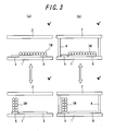
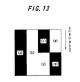
- Fig. 13 The test pattern displayed by a passive matrix driving method is shown in Fig. 13.
- (a) is a solid black pattern region
- (b) is a solid white pattern region
- (c) - (f) are regions being influenced by the cross-talk. Detail explanation will be explained in the next section.
- Fig. 14 shows a display screen on which the test pattern is displayed
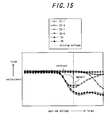
- Fig. 15 illustrates a measured typical reflectance - applied voltage characteristic.
- 5 x 5 measuring points were allocated as shown in Fig. 14, and reflectance at respective points was measured under such a condition that the test pattern was displayed by applying a writing voltage, which is gradually increased from 0V.
- reflectance of respective regions was determined as an average value of respective square portions, and, in Fig. 15, a characteristic curve was indicated in a graph, whose abscissa axis is the applied voltage and whose longitudinal axis is reflectance.
- respective lines shown in Fig. 15 will be explained. It should be noted that the matrix driving method is performed in the manner shown in the following Table 1.
- a potential difference is described in such a manner that a potential applied to an electrode at a column side is assumed to be +. For example, if a voltage of 0V is applied to column side and a voltage of 50V is applied to a row side, a potential difference between electrodes is -50V.
- a voltage of 0(V) is applied, and, when the row is not selected; a voltage of -V/2 is applied during a front half of the scanning operation and a cross-talk voltage of V/2 is applied during a back half of the scanning operation.
- the row of this region is selected at a front half of the scanning operation, but, if the applied voltage is made larger, it is largely affected by the cross-talk generating during the back half of the scanning operation. Therefore, a white color display of this region is not maintained and is transferred to a black color display.
- a voltage of 0(V) is applied, and, when the row is not selected, a voltage of V/2 is applied during a front half of the scanning operation and a cross-talk voltage of -V/2 is applied during a back half of the scanning operation.
- the row of this region is selected at a front half of the scanning operation, but, if the applied voltage is made larger, it is largely affected by the cross-talk generating during the back half of the scanning operation. Therefore, a black color display of this region is not maintained and is transferred to a white color display.
- a voltage of 0(V) is applied, and, when the row is not selected, a voltage of V/2 is applied during a front half of the scanning operation and a cross-talk voltage of -V/2 is applied during a back half of the scanning operation.
- the row of this region is selected at a back half of the scanning operation, but, since a voltage of 0(V) is selected which is differed from the region 1-5, an affection of the cross-talk generating during a front half of the scanning operation remains. Therefore, if the applied voltage is made larger, a white color display of this region is not maintained and is transferred to a black color display.
- this region maintains a white color display, and this white color display is a standard of white color in various display method.
- this region maintains a black color display, and this black color display is a standard of black color in various display method.
- the region 22-1 As an important evaluation item for performing a gray level display, there is a contrast. Most important region among respective regions is the region 22-1. No matter what a minimum reflectance of black color is low, since the region 22-1 is shifted to a white color side due to an influence of the cross-talk, a contrast is restricted by reflectance of this region. The cross-talk is largely affected even in the region 21-1, but a variation due to the cross-talk occurs at a high voltage side as compared with the region 22-1. Since an object is to obtain an excellent display in a lower voltage so as to reduce power consumption, the cross-talk of the region 21-1 is negligible.
- the evaluation method of this experiment is defined as follows.
- Normal contrast is indicated as a ratio between maximum reflectance of a white color and minimum reflectance of a black color, but, in this experiment, it was defined as follows with taking into consideration of the items mentioned above. That is, a contrast was defined as a ratio between reflectance of minimum (maximum: in the case of black deleting and white writing) level of a line 22-1 and reflectance of white (black: in the case of black deleting and white writing) display at that time.
- black deleting and white writing means "deleting - rewriting method" in which a deleting operation is performed in such a manner that a display state becomes black, and then a rewriting operation is performed in such a manner that a portion to be displayed as a white color becomes white.
- deleting - rewriting method in which a deleting operation is performed in such a manner that a display state becomes white, and then a rewriting operation is performed in such a manner that a portion to be displayed as a black color becomes black is called as "white deleting and black writing". It should be noted that it is better to make a contrast higher.
- margin of driving voltage (lateral line with double-headed arrow in Fig. 15)
- a margin of the driving voltage was defined as a width of the line 22-1, at which a difference on the line 22-1 between reflectance of minimum (maximum: in the case of black deleting and white writing) level and reflectance of white (black: in the case of black deleting and white writing) display is increased (decreased: in the case of black deleting and white writing) by 10%. It should be noted that it is better to make a margin wider.
- a pulse driving voltage was investigated under the condition such that the contrast and the margin of the driving voltage defined as mentioned above were used as the indexes.
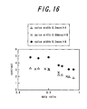
- V 0 which was not larger than a threshold value, was 0(V).
- a contrast was measured when a duty ratio of respective pulse voltages was varied in various manner.
- the results are shown in Fig. 16.
- the duty ratio in an abscissa axis is indicated by a logarithm scale. From the results shown in Fig. 16, it is understood that a contrast is decreased, if the duty ratio exceeds 0.9, and that it is preferred to make the duty ratio as small as possible.
- the driving voltage use was made of three kinds of pulse voltages such as four pulses each having a pulse width of 0.2 msec, eight pulses each having a pulse width of 0.08 msec and eight pulses each having a pulse width of 0.2 msec, and a margin was measured when a duty ratio of respective pulse voltages was varied in various manner.
- the results are shown in Fig. 17. From the results shown in Fig. 17, since the margin is larger if the duty ratio is smaller, it is understood that it is preferred to make the duty ratio as small as possible.
- a passive matrix panel which was constructed by row electrodes 31-1 to 31-n and column electrodes 32-1 to 32-m, was manufactured.
- the row electrodes 31-1 to 31-n are selected one by one to rewrite one frame.
- Fig. 20 shows a driving method of a comparative example 1
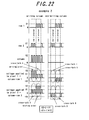
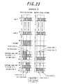
- Figs. 21 to 23 illustrate a driving method of examples 1 to 3 respectively.
- the driving methods shown in Figs. 20 to 23 for the sake of simplicity of the explanation, the explanation is made to the passive matrix panel with two rows and two columns as is the sama as the examples shown in Figs.
- a driving operation is performed in such a manner that a pulse voltage is applied two times for one rewriting operation (ON-OFF-ON-OFF).
- a voltage waveform applied to row, column and respective electrodes and a voltage waveform applied to respective pixels are shown at a first row rewriting operation (selected) and a second row rewriting operation (selected).
- a pulse was applied two times as a column rewriting voltage, while a row selected voltage was the same as the known one.
- pulse voltages on a cross-talk 2 and a cross-talk 4 applied to a non-writing pixel vary their polarity in such a manner that one peak is +V1 and the other peak is -V1, and a peak-to-peak value is large.
- the display media are easy to move and are strongly affected by the cross-talk, to that a contrast was deteriorated.
- a pulse was applied two times as a row selected voltage, while a column rewriting voltage was the same as the known one.
- pulse voltages on cross-talk 1 to 3 and cross-talk 4 to 6 applied to a non-writing pixel have the same polarity. That is, a polarity of the cross-talk 1 and 6 is constant in such a manner that one peak is 0V and the other peak is -V1; a polarity of the cross-talk 2 and 4 is constant as +V1; and a polarity of the cross-talk 3 and 5 is constant as -V1.
- a peak-to-peak value of the rewriting voltage applied to a pixel is a half of the rewriting voltage (V2-V1). Therefore, a contrast is maintained as an excellent state, but an effect for an object of varying a dividing number of the applied pulse voltage from one time to plural times is reduced.
- a polarity of the cross-talk 1 and 6 is constant as 0V; a polarity of the cross-talk 2 and 4 is constant in such a manner that one peak is +V and the other peak is 0V; and a polarity of the cross-talk 3 and 5 is constant in such a manner that one peak is 0V and the other peak is -V1.
- the cross-talk is influenced in such a manner that an improving effect of the example 1 is maintained as it is and a peak-to-peak value of the rewriting voltage is two times larger than that of the example 1. Therefore, a rewriting operation of the rewriting pixel can be performed effectively, and it was possible to prevent a variation of the non-rewriting pixel due to an influence of the cross-talk.
- a row (scam) driving voltage and a column driving voltage are constituted by a pulse train having same cycle and same duty respectively, and a phase of respective pulse train of the row driving voltage and the column driving voltage is inverted when a column at row side is selected.
- pulse voltages on cross-talk 1 to 3 and cross-talk 4 to 6 applied to a non-writing pixel have the same polarity.
- a polarity of the cross-talk 1 and 6 is constant in such a manner that one peak is 0V and the other peak is -V1; a polarity of the cross-talk 2 and 4 is constant as in such a manner that one peak is +V and the other peak is 0V; and a polarity of the cross-talk 3 and 5 is constant in such a manner that one peak is 0V and the other peak is -V1.
- the cross-talk is influenced in such a manner that an improving effect of the examples 1 and 2 is maintained as it is and a peak-to-peak value of the rewriting voltage is three times larger than that of the example 1. Therefore, a rewriting operation of the rewriting pixel can be performed effectively, and it was possible to prevent a variation of the non-rewriting pixel due to an influence of the cross-talk more preferably.
- a test pattern was displayed on the passive matrix panel with 320 lines at row (scan) side and 320 lined at column side shown in Fig. 24a, which was driven by the driving method of the examples 1 to 3 and the comparative example 1 mentioned above, and reflection of a rewriting (no cross-talk) area and reflection of a cross-talk area (cross-talk 4 to 6 mentioned above) shown in Fig. 24b were measured by an optical densitometer (RD-1 produced by GretagMacbeth AG).
- the driving conditions were as follows. That is, the number of applied rewriting voltages for 1 pixel was 8; it was driven by the driving voltage at which a contrast was maximum and an influence of the cross-talk 4 was minimum; and non-selected column/row was biased by 1/2 of the driving voltage.
- Table 2 The results are shown in the following Table 2.
- the image display device which is an object of the driving method according to the invention, is applicable to the image display unit for mobile equipment such as notebook personal computers, PDAs, cellular phones, handy terminal and so on; to the electric paper for electric book, electric newspaper and so on; to the bulletin boards such as signboards, posters, blackboards and so on; to the image display unit for electric calculator, home electric application products, auto supplies and so on; to the card display unit for point card, IC card and so on; and to the display unit for electric POP, electric advertisement, electric price tag, electric bin tag, electric musical score, RF-ID device and so on.
- mobile equipment such as notebook personal computers, PDAs, cellular phones, handy terminal and so on
- the electric paper for electric book, electric newspaper and so on to the bulletin boards such as signboards, posters, blackboards and so on
- to the image display unit for electric calculator home electric application products, auto supplies and so on
- to the card display unit for point card, IC card and so on and to the display unit for electric POP,
Applications Claiming Priority (6)
| Application Number | Priority Date | Filing Date | Title |
|---|---|---|---|
| JP2004125988 | 2004-04-21 | ||
| JP2004125986 | 2004-04-21 | ||
| JP2004126027 | 2004-04-21 | ||
| JP2004239632A JP5129919B2 (ja) | 2004-04-21 | 2004-08-19 | 画像表示装置の駆動方法 |
| JP2004239661A JP4124180B2 (ja) | 2004-04-21 | 2004-08-19 | 画像表示装置の駆動方法 |
| PCT/JP2005/007542 WO2005104078A1 (fr) | 2004-04-21 | 2005-04-20 | Procede de commande d’affichage d’informations |
Publications (2)
| Publication Number | Publication Date |
|---|---|
| EP1758087A1 true EP1758087A1 (fr) | 2007-02-28 |
| EP1758087A4 EP1758087A4 (fr) | 2008-07-30 |
Family
ID=35197219
Family Applications (1)
| Application Number | Title | Priority Date | Filing Date |
|---|---|---|---|
| EP05734545A Ceased EP1758087A4 (fr) | 2004-04-21 | 2005-04-20 | Procede de commande d'affichage d'informations |
Country Status (2)
| Country | Link |
|---|---|
| EP (1) | EP1758087A4 (fr) |
| WO (1) | WO2005104078A1 (fr) |
Families Citing this family (2)
| Publication number | Priority date | Publication date | Assignee | Title |
|---|---|---|---|---|
| EP2054758A2 (fr) * | 2006-08-17 | 2009-05-06 | Koninklijke Philips Electronics N.V. | Dispositifs d'affichage électrophorétiques |
| JP5879752B2 (ja) * | 2011-06-02 | 2016-03-08 | 船井電機株式会社 | 表示装置 |
Citations (2)
| Publication number | Priority date | Publication date | Assignee | Title |
|---|---|---|---|---|
| EP1117086A2 (fr) * | 2000-01-12 | 2001-07-18 | Nec Corporation | Dispositif d'affichage écrivant les données de suppression pendant la période de suppression verticale |
| US20030063076A1 (en) * | 2001-09-28 | 2003-04-03 | Fuji Xerox Co., Ltd. | Image display device |
Family Cites Families (3)
| Publication number | Priority date | Publication date | Assignee | Title |
|---|---|---|---|---|
| JP3633152B2 (ja) * | 1996-11-14 | 2005-03-30 | ソニー株式会社 | アクティブマトリクス表示装置およびその駆動方法 |
| JP4397157B2 (ja) * | 2002-02-15 | 2010-01-13 | 株式会社ブリヂストン | 画像表示装置 |
| JP4304925B2 (ja) * | 2002-06-28 | 2009-07-29 | セイコーエプソン株式会社 | 電気光学装置及びその駆動方法並びに電子機器 |
-
2005
- 2005-04-20 WO PCT/JP2005/007542 patent/WO2005104078A1/fr active Application Filing
- 2005-04-20 EP EP05734545A patent/EP1758087A4/fr not_active Ceased
Patent Citations (2)
| Publication number | Priority date | Publication date | Assignee | Title |
|---|---|---|---|---|
| EP1117086A2 (fr) * | 2000-01-12 | 2001-07-18 | Nec Corporation | Dispositif d'affichage écrivant les données de suppression pendant la période de suppression verticale |
| US20030063076A1 (en) * | 2001-09-28 | 2003-04-03 | Fuji Xerox Co., Ltd. | Image display device |
Non-Patent Citations (1)
| Title |
|---|
| See also references of WO2005104078A1 * |
Also Published As
| Publication number | Publication date |
|---|---|
| EP1758087A4 (fr) | 2008-07-30 |
| WO2005104078A1 (fr) | 2005-11-03 |
Similar Documents
| Publication | Publication Date | Title |
|---|---|---|
| US7554716B2 (en) | Information display panel | |
| US8044926B2 (en) | Information display panel | |
| US7973761B2 (en) | Method of driving information display panel | |
| EP1780590A1 (fr) | Affichage d'informations | |
| US20110234575A1 (en) | Method of Driving Information Display Device | |
| US7483201B2 (en) | Particles for display media, information display panel and information display device, utilizing the particles for display media | |
| EP2234095A1 (fr) | Procédé de commande de panneau d'affichage d'informations et panneau d'affichage d'informations | |
| EP1770434B1 (fr) | Dispositif d'affichage et sa procédé de fabrication | |
| JP4939778B2 (ja) | 情報表示用パネルの駆動方法 | |
| EP1758087A1 (fr) | Procede de commande d'affichage d'informations | |
| JP5129919B2 (ja) | 画像表示装置の駆動方法 | |
| US7755600B2 (en) | Method for driving information display device and information display device using the method | |
| EP1662305A2 (fr) | Dispositif d'affichage d'image, procede de fabrication d'un ecran d'affichage d'image, et ecran d'affichage d'image | |
| JP2005331936A (ja) | 情報表示装置の駆動方法 | |
| CN100487781C (zh) | 信息显示装置的驱动方法 | |
| EP1715376B1 (fr) | Affichage d'informations | |
| EP1739477A1 (fr) | Panneau d'affichage d'information | |
| EP2065755A1 (fr) | Procédé de commande de panneau d'affichage d'informations | |
| EP1785768A1 (fr) | Panneau d'affichage d'information | |
| EP1870768A1 (fr) | Panneau d affichage d informations | |
| EP2178077A1 (fr) | Procédé de commande de panneau d'affichage d'informations | |
| JP4124180B2 (ja) | 画像表示装置の駆動方法 | |
| EP2296134A1 (fr) | Procédé pour commander un panneau d'affichage d'informations | |
| EP2431804A1 (fr) | Particule pour support d'affichage |
Legal Events
| Date | Code | Title | Description |
|---|---|---|---|
| PUAI | Public reference made under article 153(3) epc to a published international application that has entered the european phase |
Free format text: ORIGINAL CODE: 0009012 |
|
| 17P | Request for examination filed |
Effective date: 20061102 |
|
| AK | Designated contracting states |
Kind code of ref document: A1 Designated state(s): DE FR |
|
| RIN1 | Information on inventor provided before grant (corrected) |
Inventor name: NIHEI, NORIOC/O BRIDGESTONE CORPORATION TECHNICAL Inventor name: TSUCHIE, SHUHEI Inventor name: MASUTANI, MAKI |
|
| DAX | Request for extension of the european patent (deleted) | ||
| RBV | Designated contracting states (corrected) |
Designated state(s): DE FR |
|
| A4 | Supplementary search report drawn up and despatched |
Effective date: 20080702 |
|
| 17Q | First examination report despatched |
Effective date: 20081103 |
|
| REG | Reference to a national code |
Ref country code: DE Ref legal event code: R003 |
|
| STAA | Information on the status of an ep patent application or granted ep patent |
Free format text: STATUS: THE APPLICATION HAS BEEN REFUSED |
|
| 18R | Application refused |
Effective date: 20120407 |