EP1748523B1 - Broadband high frequency slip-ring system - Google Patents
Broadband high frequency slip-ring system Download PDFInfo
- Publication number
- EP1748523B1 EP1748523B1 EP06253823A EP06253823A EP1748523B1 EP 1748523 B1 EP1748523 B1 EP 1748523B1 EP 06253823 A EP06253823 A EP 06253823A EP 06253823 A EP06253823 A EP 06253823A EP 1748523 B1 EP1748523 B1 EP 1748523B1
- Authority
- EP
- European Patent Office
- Prior art keywords
- ring
- slip
- rings
- impedance
- pcb
- Prior art date
- Legal status (The legal status is an assumption and is not a legal conclusion. Google has not performed a legal analysis and makes no representation as to the accuracy of the status listed.)
- Not-in-force
Links
Images


Classifications
-
- H—ELECTRICITY
- H01—ELECTRIC ELEMENTS
- H01R—ELECTRICALLY-CONDUCTIVE CONNECTIONS; STRUCTURAL ASSOCIATIONS OF A PLURALITY OF MUTUALLY-INSULATED ELECTRICAL CONNECTING ELEMENTS; COUPLING DEVICES; CURRENT COLLECTORS
- H01R39/00—Rotary current collectors, distributors or interrupters
- H01R39/02—Details for dynamo electric machines
- H01R39/08—Slip-rings
- H01R39/10—Slip-rings other than with external cylindrical contact surface, e.g. flat slip-rings
-
- H—ELECTRICITY
- H01—ELECTRIC ELEMENTS
- H01P—WAVEGUIDES; RESONATORS, LINES, OR OTHER DEVICES OF THE WAVEGUIDE TYPE
- H01P1/00—Auxiliary devices
- H01P1/06—Movable joints, e.g. rotating joints
-
- H—ELECTRICITY
- H01—ELECTRIC ELEMENTS
- H01R—ELECTRICALLY-CONDUCTIVE CONNECTIONS; STRUCTURAL ASSOCIATIONS OF A PLURALITY OF MUTUALLY-INSULATED ELECTRICAL CONNECTING ELEMENTS; COUPLING DEVICES; CURRENT COLLECTORS
- H01R39/00—Rotary current collectors, distributors or interrupters
- H01R39/02—Details for dynamo electric machines
- H01R39/18—Contacts for co-operation with commutator or slip-ring, e.g. contact brush
- H01R39/24—Laminated contacts; Wire contacts, e.g. metallic brush, carbon fibres
-
- H—ELECTRICITY
- H01—ELECTRIC ELEMENTS
- H01R—ELECTRICALLY-CONDUCTIVE CONNECTIONS; STRUCTURAL ASSOCIATIONS OF A PLURALITY OF MUTUALLY-INSULATED ELECTRICAL CONNECTING ELEMENTS; COUPLING DEVICES; CURRENT COLLECTORS
- H01R12/00—Structural associations of a plurality of mutually-insulated electrical connecting elements, specially adapted for printed circuits, e.g. printed circuit boards [PCB], flat or ribbon cables, or like generally planar structures, e.g. terminal strips, terminal blocks; Coupling devices specially adapted for printed circuits, flat or ribbon cables, or like generally planar structures; Terminals specially adapted for contact with, or insertion into, printed circuits, flat or ribbon cables, or like generally planar structures
- H01R12/50—Fixed connections
- H01R12/51—Fixed connections for rigid printed circuits or like structures
- H01R12/52—Fixed connections for rigid printed circuits or like structures connecting to other rigid printed circuits or like structures
- H01R12/523—Fixed connections for rigid printed circuits or like structures connecting to other rigid printed circuits or like structures by an interconnection through aligned holes in the boards or multilayer board
-
- H—ELECTRICITY
- H01—ELECTRIC ELEMENTS
- H01R—ELECTRICALLY-CONDUCTIVE CONNECTIONS; STRUCTURAL ASSOCIATIONS OF A PLURALITY OF MUTUALLY-INSULATED ELECTRICAL CONNECTING ELEMENTS; COUPLING DEVICES; CURRENT COLLECTORS
- H01R35/00—Flexible or turnable line connectors, i.e. the rotation angle being limited
- H01R35/02—Flexible line connectors without frictional contact members
- H01R35/025—Flexible line connectors without frictional contact members having a flexible conductor wound around a rotation axis
-
- H—ELECTRICITY
- H01—ELECTRIC ELEMENTS
- H01R—ELECTRICALLY-CONDUCTIVE CONNECTIONS; STRUCTURAL ASSOCIATIONS OF A PLURALITY OF MUTUALLY-INSULATED ELECTRICAL CONNECTING ELEMENTS; COUPLING DEVICES; CURRENT COLLECTORS
- H01R39/00—Rotary current collectors, distributors or interrupters
- H01R39/02—Details for dynamo electric machines
- H01R39/08—Slip-rings
-
- H—ELECTRICITY
- H01—ELECTRIC ELEMENTS
- H01R—ELECTRICALLY-CONDUCTIVE CONNECTIONS; STRUCTURAL ASSOCIATIONS OF A PLURALITY OF MUTUALLY-INSULATED ELECTRICAL CONNECTING ELEMENTS; COUPLING DEVICES; CURRENT COLLECTORS
- H01R39/00—Rotary current collectors, distributors or interrupters
- H01R39/64—Devices for uninterrupted current collection
Definitions
- the present invention is generally directed to a contact-type slip-ring system that is utilized to transfer signals from a stationary reference frame to a moving reference frame and, more specifically, to a contact-type slip-ring system that is suitable for high data rate communication.
- Contact-type slip-rings have been widely used to transmit signals between two frames that move in rotational relation to each other.
- Prior art slip-rings of this nature have utilized precious alloy conductive probes to make contact with a rotating ring system. These probes have traditionally been constructed using round-wire, composite materials, button contacts or multi-filament conductive fiber brushes.
- the corresponding concentric contact rings of the slip-ring are typically shaped to provide a cross-section shape appropriate for the sliding contact. Typical ring shapes have included V-grooves, U-grooves and flat rings. Similar schemes have been used with systems that exhibit translational motion rather than rotary motion.
- Impedance discontinuities can occur throughout the slip-ring wherever different forms of transmission lines interconnect and have different surge impedances.
- Significant impedance mismatches often occur where transmission lines interconnect a slip-ring to an external interface, at the brush contact structures and where the transmission lines connect those brush contact structures to their external interfaces.
- Severe distortion to high-frequency signals can occur from either of those impedance mismatched transitions of the transmission lines. Further, severe distortion can also occur due to phase errors from multiple parallel brush connections.
- a contracting ring system comprising a dielectric material with a first side and a second side; a plurality of concentric spaced conductive rings located on the first side of the dielectric material, wherein the conductive rings include an inner ring and an outer ring; and a first ground plane located on the second side of the dielectric material, characterised in that the width of the inner ring is greater than the width of the outer ring; and the widths of the inner and outer rings are selected to substantially equalize the electrical lengths of the inner and outer rings.
- a groove is formed in the dielectric material on at least one side of the outer ring to cause an increase in a signal propagation velocity of the outer ring.
- a second ground plane may be formed in the dielectric material between the inner ring and the first ground plane, and the second ground plane, when implemented, causes a decrease in a signal propagation velocity of the inner ring.
- the thicknesses of the inner and outer rings may be different.
- the surface finishes of the inner and outer rings may be different.
- the inner and outer rings may provide a differential pair of a transmission line.
- the inner and outer rings may provide a non-differential transmission line and the non-differential transmission line may be a coplanar waveguide.
- Embodiments of the invention may further comprise a plurality of terminators located to reduce reflections attributable to impedance discontinuities.
- the terminators may be at least one of surface mount components, embedded passive components or components created using strip-line techniques.
- the terminators may be positioned within vias.
- the embedded passive components may be thin-film components.
- a broadband contacting slip-ring system is designed for high-speed data transmission over a frequency range from DC to several GHz.
- Embodiments of the present invention employ a conductive printed circuit board (PCB) slip-ring platter that utilizes high-frequency materials and techniques and an associated transmission line that interconnects conductive rings of the PCB slip-ring platter to an external interface.
- Embodiments of the present invention may also include a contacting probe system that also utilizes PCB construction and high-frequency techniques to minimize degradation of signals attributable to high-frequency and surge impedance effects.
- the contacting probe system includes a transmission line that interconnects the probes of the contacting probe system to an external interface, again utilizing various techniques to minimize degradation of signals due to high-frequency and surge impedance effects.
- Various embodiments of the present invention address the difficulty of controlling factors that constrain high-frequency performance of a slip-ring. Specifically, embodiments of the present invention control the impedance of transmission line structures and address other concerns related to high-frequency reflection and losses.
- One embodiment of the present invention addresses key problem areas related to high-frequency reflections and losses associated with the sliding electrical contact system of slip-rings.
- Various embodiments of the present invention utilize a concentric ring system of flat conductive rings and flat interdigitated precious metal electrical contacts. Both structures are fabricated utilizing PCB materials and may implement microstrip and strip-line transmission lines and variations thereof.
- utilizing a flat form brush contact provides significant benefits related to high-frequency slip-rings, as compared to round wire contacts and other contact forms. These benefits include: reduced skin effect, as larger surface areas tend to reduce high-frequency losses; lower inductance, as a flat cross-section tends to reduce inductance and high-frequency loss; lower surge impedance, which is more compatible with slip-ring differential impedances; higher compliance (low spring rate), which is tolerant of axial run-out of a slip-ring platter; compatibility with surface mount PCB technology; and high lateral rigidity, which allows brushes to run accurately on a flat ring system.
- High lateral rigidity is generally desirable to create a slip-ring contact system that operates successfully with a flat ring system.
- a flat ring system can readily utilize PCB technology in the creation of the ring system.
- PCB technology is capable of providing a well controlled impedance characteristic that can be of significantly higher impedance value than allowed by prior art techniques. This higher impedance makes it possible to match the characteristic impedance of common transmission lines, again addressing one of the problems associated with high-frequency data transmission.
- Interdigitated contacts i.e., bifurcated contacts, trifurcated contacts or contacts otherwise divided into multiple parallel finger contacts, have other significant advantages germane to slip-ring operation.
- Parallel contact points are a traditional feature of slip-rings from the design standpoint of providing acceptably low dynamic resistance.
- dynamic noise can have a significant inductive component from the wiring necessary to implement multiple parallel contacts.
- Flat brush contacts offer multiple low inductance contact points operating in parallel and provide a significant improvement in dynamic noise performance.
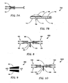
- a particular implementation of multiple flat brush contacts 200 is a pair of such brushes 202 and 204 mounted opposing each other on a PCB 206 and fed through a central eyelet or via 208.
- This implementation also has high-frequency performance benefits.
- the central eyelet 208 assures equal length transmission lines and in-phase signals to both brushes 202 and 204, as well as surge impedances favorable to impedance matching of slip-rings and low loss.
- the location of the opposing contact brush tips in close proximity helps to reduce phasing errors from the slip-ring.
- the central via 208 also allows for visual alignment verification of the contact brushes 202 and 204 to a ring, e.g., ring 106A, which is a highly desirable feature that simplifies slip-ring assembly.
- center-fed brush structures 702 and 704 can be optimally used in differential transmission lines.
- the transmission line geometry shown is typically implemented with a multi-layer PCB 700.
- the flat brush contacts 702 and 704 are surface-mounted to a microstrip structure 705 over a ground plane 710.
- the connection between the brushes 702 and 704 and the external input terminals takes the form of an embedded microstrip 712.
- the size and spacing of the brush microstrips 705 and the embedded microstrip transmission line 712 that feeds them is dictated by the necessity to match the impedance of the external transmission line and associated slip-ring.
- the via holes for connection of external transmission lines and associated central feed via 708 completely penetrate the PCB 700 and have relief areas 714 in the ground plane 710 for electrical isolation.
- Two PCBs can be bonded back-to-back to feed two slip-rings, with the vias penetrating both boards in an analogous fashion.
- multiple brush structures can be implemented utilizing PCB techniques, as described above, to create transmission line sections of the correct impedance.
- the "crossfeed" transmission lines 802 and 804 are designed for a differential impedance of 50 Ohms, matching the external feedline.
- the parallel connections to the brush structures are by means of equal length transmission lines 806 and 810.
- Such transmission lines that provide in-phase signals to the brush structures are referred to in this document as "zero-degree phasing lines," in keeping with a similar expression used for phased antenna arrays.
- the impedance of these "zero-degree phasing lines" is twice that of the "crossfeed lines," or 100 Ohms.
- the differential impedance of the slip-ring utilized with a contact structure 800 is then two times that of the phasing lines 806 and 810, or 200 Ohms.
- a general solution to parallel feed of N contact structures establishes the differential impedance of the phasing lines as N times the input impedance.
- a gradated impedance transmission line 900 can be used as a matching section between dissimilar impedances.
- a diagram illustrates a gradated impedance matching section, which shows a tapered parallel differential transmission line 900. Tapering the traces 902 and 904 is one method of continuously varying the impedance, which minimizes the magnitude of the reflections that would otherwise result from abrupt impedance discontinuities.
- Fig. 10 illustrates the use of gradated impedance transmission lines as a solution for ameliorating the effects of dissimilar impedance values.
- the differential impedance of the slip-ring associated with the contact system is too low to conveniently match the phasing lines, as described in conjunction with Fig. 8 .
- the taper of the crossfeed lines 1002 and 1004 allows the impedance of the transmission line to be gradually reduced to an intermediate value of impedance between that of the rings of the slip-ring platter and the external transmission line.
- the taper of the zero-degree phasing lines 1006 and 1010 allows the impedance to be gradually increased from that of the slip-ring to match the intermediate value described above.
- the net effect of utilizing gradated impedance matching sections is to reduce the magnitude of the reflections from what would otherwise be substantial impedance mismatches.
- the minimizing of impedance discontinuities is desirable from the standpoint of preserving signal integrity of high-speed data waveforms.
- FIG. 11 Another technique for constructing a contact system for slip-rings functioning beyond one GHz is shown in Fig. 11 .
- This technique utilizes a microstrip contact 1100 to preserve the transmission line characteristics to within a few millimeters of the slip-ring before transitioning to the contacts 1102 and 1104.
- the microstrip contact 1100 acts as a cantilever spring to provide correct brush force, as well as providing an impedance controlled transmission line.
- the microstrip contact 1100 acts simultaneously as a transmission line, a spring and a brush contact, with performance advantages beyond one GHz.
- the embodiment of Fig. 12 which depicts the contact 1100 of Fig. 11 in conjunction with a slip-ring platter 1120, functions to provide a single high-speed differential data channel of a broadband slip-ring.
- Systems that implement a broadband slip-ring platter with a flat interdigitated brush contact system are typically implemented utilizing multi-layer PCB techniques, although other techniques are also possible.
- High-frequency performance is enhanced by the use of low dielectric constant substrates and controlled impedance transmission lines utilizing microstrip, strip-line, coplanar waveguide and similar techniques.
- the use of balanced differential transmission lines is an important tool from the standpoint of controlling electromagnetic emission and susceptibility, as well as common-mode interference.
- Microstrip, strip-line and other microwave construction techniques also promote accurate impedance control of the transmission line structures, a factor vital to the wide bandwidths necessary for high-frequency and digital signaling. A specific implementation depends primarily upon the desired impedance and bandwidth requirements.
- Figs. 13A-13B show an electrical diagram and a partial cross-section, respectively, of a slip-ring platter 1300 utilizing microstrip construction, with conductive rings 1302A and 1302B etched on one side of a PCB dielectric material 1304, with a ground plane 1310 on the opposite side.
- the PCB material 1304 is chosen for the desired dielectric constant that is appropriate for the desired impedance of the slip-ring platter 1300.
- Connections between the conductive rings 1302A and 1302B and the external transmission lines are accomplished by embedded microstrips 1306A and 1306B, respectively.
- Microstrips 1306A and 1306B are typically routed to a via or surface pad for attachment to wiring or other transmission line.
- connections between the feedlines 1306A and 1306B and the rings 1302A and 1302B are provided by vias that run between the two layers.
- the structure shown is typically a three-layer structure, or five to six layers if constructed as a double-sided slip-ring platter.
- the ground plane 1310 can be a solid or a mesh construction depending upon whether the ground plane is to act as an additional impedance variable and/or to control board distortion.
- Negative barrier 1320 i.e., a groove machined between the rings, accomplishes some of the functions of a more traditional barrier, such as increasing the surface creep distance for dielectric isolation and to providing physical protection against larger pieces of conductive debris.
- the negative barrier 1320 used in a high-frequency slip-ring platter also has the feature of decreasing the effective dielectric constant of the ring system by replacing solid dielectric with air. The electrical advantage of this feature is that it allows higher impedance slip-ring platters to be constructed than would otherwise be practical for a given dielectric.
- the negative barrier 1320 may also be implemented to provide velocity compensation, as is further described below.
- the rings 1302A and 1302B can be fed either single-ended and referenced to the ground plane 1310 or differentially between adjacent rings.
- the feedlines 1306A and 1306B can be either constant width traces sized appropriately for the desired impedance or can be gradated impedance transmission lines to aid in matching dissimilar impedances.
- the PCB slip-ring construction provides good high-frequency performance to frequencies of several hundred MHz, depending upon the physical size of the slip-ring platter and the chosen materials.
- the largest constraint to the upper frequency limit of such a slip-ring platter is imposed by resonance effects as the transmission lines become a significant fraction of the wavelength of the desired signal.
- reasonable performance can be expected up to a ring circumference of about one-tenth the electrical wavelength of the signal with reasonable values of insertion loss and standing wave ratio.
- Fig. 14 shows a feed system 1400 that uses differential transmission lines and Fig. 15 shows a cross-section of a PCB slip-ring platter that incorporates the feed method. Two phasing lines and associated feedpoints are shown in the example, although three or more phasing lines can be used with appropriate allowance to matching the impedances.
- the transmission line to rings 1402 and 1404 are connected to points 1401 and 1403, respectively, in both Figs. 14 and 15 .
- the crossfeed transmission lines 1406 and 1408 are designed to match the impedance of the feedline, 50 Ohms in this example.
- the parallel combination of phasing lines 1410A and 1410B and 1412A and 1412B are also designed to match the 50 Ohm impedance, or 100 Ohms individually.
- Each phasing line connection sees a parallel section of the rings 1402 and 1404, which, in this example, are designed for a 200 Ohm differential impedance. Other combinations are possible as well with appropriate adjustments to match impedances.
- the phasing line impedance is N*Z and the ring impedance is 2*N*Z. Achieving higher impedance values is facilitated by the use of low dielectric constant materials.
- the phasing lines shown in Fig. 15 benefit from the proximity of the air in the negative barrier to achieve a lower dielectric coefficient and higher differential impedance.
- gradated impedance phasing line sections facilitates multi-point connections to rings 106A and 106B of PCB slip-ring platter 102.
- This method simplifies the construction of the PCB slip-ring as the phasing lines are external to the ring and are readily connected in parallel at the crossfeed transmission line.
- the gradated impedance matching sections allow the construction of slip-rings with smooth impedance profiles, which improves passband flatness and signal distortion due to impedance discontinuities.
- the use of gradated impedance phasing lines is generally a desirable feature when constructing broadband PCB slip-rings 100.
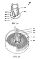
- Figs. 16 and 17 depict a rotary shaft 1600, for receiving a plurality of slip-ring platter assemblies 100, that is advantageously designed to facilitate construction of a slip-ring, while addressing three typical concerns encountered in the manufacturing of these devices.
- the shaft allows for control of axial positioning of the platters without tolerance stack-up, control of radial positioning of the platter slip-rings and wire and lead management.
- a significant difficulty when mounting slip-ring platters to a rotary shaft is avoiding tolerance stack-up that is inherent with many slip-ring mounting methods, e.g., those using spacers.
- Wire and lead management is also a perennial problem with the manufacture of most slip-rings as wire congestion increases with each additional platter.
- the rotary shaft 1600 includes a number of steps that address the above-referenced issues.
- the shaft 1600 may be a computerized numerical control (CNC) manufactured component with a series of concentric grooves machined to produce a helical arrangement of mounting lands/pads 1602-1612 for the platters 102 of the slip-ring system.
- CNC computerized numerical control
- the axial positioning of the grooves on the shaft 1600 are a function of the repeatability of the machining operation, thus one side of each slip-ring is located axially to within machining accuracy with no progressive tolerance stack-up.
- the opposite side of each platter 102 is positioned with only the ring thickness tolerance as an additional factor.
- the inside diameter of the grooves is sized to provide a radial positioning surface for the inside diameter of each platter.
- the helically arranged lands/pads 1602-1612 provide mounting features for each platter 102.
- the helical arrangement provides more wire way space as each platter 102 is installed.
- the shape of wire way 1640 provides a way for grouping wiring 1650 for cable management and electrical isolation purposes.
- the shaft 1600 may be advantageously located within a cavity 1660 of a form 1670 during the construction of the multiple platter slip-ring system.
- a slip-ring system incorporating the features disclosed herein provides a high-frequency broadband slip-ring with the following points, although not necessarily simultaneously in a given implementation: the use of flat interdigitated contacts in conjunction with flat PCB slip-rings and transmission line techniques to achieve wide bandwidths; use of brush contact structures that include a central via coupled to a feedline, which provides performance advantages and allows for visual alignment verification between rings and brushes; PCB construction of differential transmission lines for multi-point feeding of slip-rings; the use of multiple flex tape phasing lines for multi-point feeding of slip-rings; the use of gradated impedance transmission line matching sections to affect impedance matching in PCB slip-rings in general and specifically in the above applications; the use of a negative barrier in PCB slip-ring platter design for its electrical isolation benefits as well as its high-frequency benefits attributable to a lower dielectric constant; the use of microstrip contacts, i.e., a flexible section of microstrip transmission line with embedded contacts to provide high-frequency performance advantages over more traditional approaches
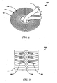
- Transmitting differential signals across a platter-style slip-ring may require addressing the problem of differing ring radii R1 and R2 of Fig. 18 of two conductors or more conductors that make up a transmission line.
- a typical platter-type slip-ring conductive rings with differing radii for each ring are implemented.
- the rings of a resulting ring pair have different physical circumferences and, thus, form a transmission line that is made up of two unequal path lengths.
- the differing physical lengths of the rings result in differing electrical lengths for the rings, with the result that differential signals carried by the rings become out of phase as they travel around the rings.
- a transmission line so constructed exhibits a host of electrical penalties, which include: degraded differential balance, increased radiation from the transmission line, increased vulnerability to common-mode signals, increased jitter and decreased digital data rate.
- the limitations exhibited by slip-rings that utilize differing radii for the rings is addressed by the application of velocity compensation techniques.
- the velocity compensation techniques result in equalization of the electrical lengths of the rings, even though the rings have differing physical lengths. In this manner, signals propagating around the slip-ring remain in-phase with respect to angular position and do not exhibit phase delay that is inherent in prior art slip-rings.
- a number of techniques may be implemented to control and equalize the propagation velocity of a differential platter slip-ring 1800, which may rotate around a rotation axis 1801. For example, since a wider ring has a lower velocity of propagation than a narrower ring, a width of inner ring 1808 may be selected to be wider than a width of outer ring 1810. In this manner, the widths of the two rings of a differential pair are adjusted to achieve an equal electrical circumference (or equal time delay). The velocity of propagation of the outer ring 1810 may also be increased by forming grooves 1812 in a dielectric 1804 on either side of the outer ring 1810.
- the grooves 1812 effectively decrease an average dielectric constant and, thus, increase the velocity of propagation of a signal carried by the outer ring 1812.
- the grooves 1812 may be, for example, cut into the dielectric 1804 on one or both sides of the outer ring 1812.
- the size of the grooves 1812 may be adjusted to cause both the inner ring 1808 and the outer ring 1812 to have the same electrical circumference and time delay, despite having different physical circumferences.
- the velocity of propagation of a ring may also be altered by changing the distance of a ring to a surrounding metal structure, such as the distance to ground plane 1802. For example, the velocity of propagation of a ring can be decreased by decreasing the distance to a ground plane.
- an additional ground plane 1806 may be incorporated within the dielectric 1804 under the inner ring 1808. The physical dimensions of the additional ground plane 1806 and the distance between the ground plane 1806 and the inner ring 1808 may then be adjusted to achieve the same electrical length or time delay as the unaltered ring of the differential pair.
- the velocity of propagation of a ring may also be affected by controlling a thickness and surface finish of the rings.
- the above described propagation velocity compensation techniques may also be used in slip-rings having one or more non-differential transmission lines, such as coplanar waveguide 1900, which may rotate about a rotation axis 1901.
- Any combination of the techniques describe above may be used to adjust a propagation velocity of inner ring 1906, middle ring 1908 and outer ring 1910 to achieve substantially equal electrical lengths for the rings 1906, 1908 and 1910, which are spaced from ground plane 1902.
- three different ring widths may be implemented to progressively increase the velocity of propagation with increasing radius of the ring.
- the velocity of propagation of the rings 1908 and 1910 can also be increased by forming grooves 1912, 1912A and 1912B into dielectric 1904.
- a secondary ground plane ring (such as shown in Fig. 18 ) may be included under the inner ring 1906 to slow the velocity of propagation of a signal carried on the ring 1906.
- the goal is to create a geometry that equalizes the electrical lengths of the concentric rings, by altering the ring width, thickness or surface finish, and/or by locally modifying the effective dielectric constant of the surrounding dielectric media and/or by adding a secondary ground plane beneath an appropriate ring.
- PCB slip-ring construction techniques can also be used to incorporate these terminations into the construction of the PCB by various techniques, e.g., by implementing surface-mount components for LCR networks, embedded passive (LCR) components within or on the PC board S/R and/or strip-line techniques to create LCR networks using the PCB traces.
- LCR embedded passive
- a termination technique for a single-ended slip-ring may include a series-shunt connection of resistor networks 2002 and 2004, as is illustrated in Fig. 20 , for a single-ended slip-ring 2000.
- a termination technique for a differential slip-ring may include a series-shunt connection of resistor networks 2102 and 2104, as is illustrated in Fig. 21 , for a differential slip-ring 2100.
- More complex networks consisting of inductive, capacitive and/or resistive (LCR) elements can be used as needed to perform necessary transformations of impedance, voltage or current.
- LCR resistive resistive
- the use of active electronic devices can also provide such transformations, in addition to signal conditioning, conversion and/or recovery.
- the incorporation of electronic components onto or into the slip-ring transmission line, as is described above, is advantageous for maintaining signal integrity.
- SMT Surface Mount Technology
- shunt elements 2206 may be installed inside a via 2204 of a PCB 2202 of slip-ring 2200. In this case, the elements 2206 are soldered at each end to achieve connection without the stray reactances that may be inherent in using other via and pad constructions.
- SMT techniques can be used for the slip-ring and contact PCBs, as well as flex tape transmission lines and intermediate connector boards.
- embedded passive components 2306 can be incorporated directly into a PCB 2302 of slip-ring 2300 or into a contact (brush block) PCB. This may be achieved by applying resistive and/or capacitive elements into appropriate intermediate layers of the PCB stack, using thin-film or other technologies. The ability to apply such components at key places in a slip-ring PCB layout is advantageous for signal integrity, from the standpoint of controlling impedance and managing reflections.
- resistors 2006 and 2008 shown in dotted form, may be effectively incorporated as embedded passive components.
- the component 2306 may be a film resistor that is deposited directly across copper traces 2304 of a layer of the PCB 2302.
- transmission line networks for microwave frequencies can be implemented using PCB strip-lines and microstrips (creating capacitors and inductors using printed circuit traces), allowing the components to be incorporated directly into the slip-ring or contact PCB as part of the lay-up without using discrete components.
Applications Claiming Priority (1)
| Application Number | Priority Date | Filing Date | Title |
|---|---|---|---|
| US11/192,910 US7142071B2 (en) | 2003-02-19 | 2005-07-29 | Broadband high-frequency slip-ring system |
Publications (3)
| Publication Number | Publication Date |
|---|---|
| EP1748523A2 EP1748523A2 (en) | 2007-01-31 |
| EP1748523A3 EP1748523A3 (en) | 2008-04-09 |
| EP1748523B1 true EP1748523B1 (en) | 2009-11-11 |
Family
ID=37310857
Family Applications (1)
| Application Number | Title | Priority Date | Filing Date |
|---|---|---|---|
| EP06253823A Not-in-force EP1748523B1 (en) | 2005-07-29 | 2006-07-20 | Broadband high frequency slip-ring system |
Country Status (8)
| Country | Link |
|---|---|
| US (1) | US7142071B2 (ja) |
| EP (1) | EP1748523B1 (ja) |
| JP (1) | JP4425248B2 (ja) |
| AT (1) | ATE448587T1 (ja) |
| CA (1) | CA2552338C (ja) |
| DE (1) | DE602006010275D1 (ja) |
| DK (1) | DK1748523T3 (ja) |
| ES (1) | ES2334055T3 (ja) |
Families Citing this family (14)
| Publication number | Priority date | Publication date | Assignee | Title |
|---|---|---|---|---|
| GB2493977A (en) * | 2011-08-26 | 2013-02-27 | Overview Ltd | Slip ring apparatus |
| CN102542170B (zh) * | 2012-01-16 | 2015-05-13 | 烟台磐能电气控制系统有限公司 | 一种得到电力系统频率滑差的方法 |
| US9306353B2 (en) | 2013-05-29 | 2016-04-05 | Moog Inc. | Integrated rotary joint assembly with internal temperature-affecting element |
| CA2932622C (en) | 2013-12-17 | 2019-05-28 | Moog Inc. | High-speed data link with planar near-field probe |
| JP5792367B1 (ja) * | 2014-08-08 | 2015-10-14 | 京楽産業.株式会社 | 遊技機 |
| US9240660B1 (en) | 2014-11-18 | 2016-01-19 | General Electric Company | Slip ring assembly and method for impedance matching high frequency signals across the slip ring assembly |
| US9528891B2 (en) | 2014-11-25 | 2016-12-27 | Hamilton Sundstrand Corporation | Slip ring containment band |
| US9735530B2 (en) * | 2015-03-10 | 2017-08-15 | General Electric Company | Apparatus and method for axially spacing conductive rings of a slip ring assembly |
| ITUB20152201A1 (it) * | 2015-07-15 | 2017-01-15 | Conductix Wampfler S R L | COLLETTORE ELETTRICO ROTANTE AD ALBERO CAVO PER ETHERNET FINO A UN Gbps |
| US9894767B1 (en) | 2016-03-20 | 2018-02-13 | Jason Krugman Products, LLC | Concentric circle printed circuit board electrical connection |
| KR102531872B1 (ko) | 2016-06-21 | 2023-05-11 | 유니버셜 인스트루먼츠 코퍼레이션 | 조립 기계를 위한 슬립 트랙 구조, 시스템 및 방법 |
| KR102542594B1 (ko) * | 2016-12-16 | 2023-06-14 | 삼성전자 주식회사 | 다층 인쇄 회로 기판 및 이를 포함하는 전자 장치 |
| US11736145B2 (en) | 2019-05-28 | 2023-08-22 | Moog Inc. | Graduated frequency response non-contacting slip ring probe |
| WO2021262984A1 (en) * | 2020-06-25 | 2021-12-30 | Blate Alex | Reconfigurable interconnection node |
Family Cites Families (4)
| Publication number | Priority date | Publication date | Assignee | Title |
|---|---|---|---|---|
| US3382387A (en) | 1968-05-07 | Gen Electric | Electrical current collection and delivery method and apparatus | |
| US5805115A (en) | 1995-08-01 | 1998-09-08 | Kevlin Corporation | Rotary microwave antenna system |
| DE10219958A1 (de) * | 2002-05-03 | 2003-12-04 | Schleifring Und Appbau Gmbh | Vorrichtung zur elektrischen Verbindung zweier gegeneinander beweglicher Einheiten |
| US6956445B2 (en) | 2003-02-19 | 2005-10-18 | Electro-Tec Corp. | Broadband high-frequency slip ring system |
-
2005
- 2005-07-29 US US11/192,910 patent/US7142071B2/en not_active Expired - Fee Related
-
2006
- 2006-07-14 CA CA2552338A patent/CA2552338C/en not_active Expired - Fee Related
- 2006-07-20 DK DK06253823.6T patent/DK1748523T3/da active
- 2006-07-20 AT AT06253823T patent/ATE448587T1/de active
- 2006-07-20 EP EP06253823A patent/EP1748523B1/en not_active Not-in-force
- 2006-07-20 ES ES06253823T patent/ES2334055T3/es active Active
- 2006-07-20 DE DE602006010275T patent/DE602006010275D1/de active Active
- 2006-07-28 JP JP2006206446A patent/JP4425248B2/ja not_active Expired - Fee Related
Also Published As
| Publication number | Publication date |
|---|---|
| JP2007042643A (ja) | 2007-02-15 |
| US7142071B2 (en) | 2006-11-28 |
| US20050258915A1 (en) | 2005-11-24 |
| CA2552338C (en) | 2012-09-04 |
| JP4425248B2 (ja) | 2010-03-03 |
| DK1748523T3 (da) | 2010-03-08 |
| ES2334055T3 (es) | 2010-03-04 |
| DE602006010275D1 (de) | 2009-12-24 |
| ATE448587T1 (de) | 2009-11-15 |
| EP1748523A3 (en) | 2008-04-09 |
| CA2552338A1 (en) | 2007-01-29 |
| EP1748523A2 (en) | 2007-01-31 |
Similar Documents
| Publication | Publication Date | Title |
|---|---|---|
| EP1748523B1 (en) | Broadband high frequency slip-ring system | |
| JP4874380B2 (ja) | 広帯域高周波スリップリングシステム | |
| EP2102948B1 (en) | High-frequency drum-style slip-ring modules | |
| EP3201997B1 (en) | High frequency rj45 plug with non-continuous planes for cross talk control | |
| CA2406428A1 (en) | Connector for high-speed communications | |
| KR101577370B1 (ko) | 마이크로웨이브 필터 | |
| CN116209136B (zh) | 一种信号传输结构、电子设备及pcb板 | |
| US20230291423A1 (en) | Communication apparatus | |
| US20220115166A1 (en) | Ac-coupling structure in electrical cabled interconnect | |
| US11736145B2 (en) | Graduated frequency response non-contacting slip ring probe | |
| CN113873740A (zh) | 传输线结构 |
Legal Events
| Date | Code | Title | Description |
|---|---|---|---|
| PUAI | Public reference made under article 153(3) epc to a published international application that has entered the european phase |
Free format text: ORIGINAL CODE: 0009012 |
|
| AK | Designated contracting states |
Kind code of ref document: A2 Designated state(s): AT BE BG CH CY CZ DE DK EE ES FI FR GB GR HU IE IS IT LI LT LU LV MC NL PL PT RO SE SI SK TR |
|
| AX | Request for extension of the european patent |
Extension state: AL BA HR MK YU |
|
| PUAL | Search report despatched |
Free format text: ORIGINAL CODE: 0009013 |
|
| AK | Designated contracting states |
Kind code of ref document: A3 Designated state(s): AT BE BG CH CY CZ DE DK EE ES FI FR GB GR HU IE IS IT LI LT LU LV MC NL PL PT RO SE SI SK TR |
|
| AX | Request for extension of the european patent |
Extension state: AL BA HR MK RS |
|
| 17P | Request for examination filed |
Effective date: 20080328 |
|
| AKX | Designation fees paid |
Designated state(s): AT BE BG CH CY CZ DE DK EE ES FI FR GB GR HU IE IS IT LI LT LU LV MC NL PL PT RO SE SI SK TR |
|
| 17Q | First examination report despatched |
Effective date: 20090424 |
|
| GRAP | Despatch of communication of intention to grant a patent |
Free format text: ORIGINAL CODE: EPIDOSNIGR1 |
|
| GRAS | Grant fee paid |
Free format text: ORIGINAL CODE: EPIDOSNIGR3 |
|
| GRAA | (expected) grant |
Free format text: ORIGINAL CODE: 0009210 |
|
| AK | Designated contracting states |
Kind code of ref document: B1 Designated state(s): AT BE BG CH CY CZ DE DK EE ES FI FR GB GR HU IE IS IT LI LT LU LV MC NL PL PT RO SE SI SK TR |
|
| REG | Reference to a national code |
Ref country code: GB Ref legal event code: FG4D |
|
| REG | Reference to a national code |
Ref country code: CH Ref legal event code: NV Representative=s name: TROESCH SCHEIDEGGER WERNER AG Ref country code: CH Ref legal event code: EP |
|
| REG | Reference to a national code |
Ref country code: IE Ref legal event code: FG4D |
|
| REF | Corresponds to: |
Ref document number: 602006010275 Country of ref document: DE Date of ref document: 20091224 Kind code of ref document: P |
|
| REG | Reference to a national code |
Ref country code: SE Ref legal event code: TRGR |
|
| REG | Reference to a national code |
Ref country code: ES Ref legal event code: FG2A Ref document number: 2334055 Country of ref document: ES Kind code of ref document: T3 |
|
| REG | Reference to a national code |
Ref country code: DK Ref legal event code: T3 |
|
| LTIE | Lt: invalidation of european patent or patent extension |
Effective date: 20091111 |
|
| PG25 | Lapsed in a contracting state [announced via postgrant information from national office to epo] |
Ref country code: LT Free format text: LAPSE BECAUSE OF FAILURE TO SUBMIT A TRANSLATION OF THE DESCRIPTION OR TO PAY THE FEE WITHIN THE PRESCRIBED TIME-LIMIT Effective date: 20091111 Ref country code: FI Free format text: LAPSE BECAUSE OF FAILURE TO SUBMIT A TRANSLATION OF THE DESCRIPTION OR TO PAY THE FEE WITHIN THE PRESCRIBED TIME-LIMIT Effective date: 20091111 Ref country code: PT Free format text: LAPSE BECAUSE OF FAILURE TO SUBMIT A TRANSLATION OF THE DESCRIPTION OR TO PAY THE FEE WITHIN THE PRESCRIBED TIME-LIMIT Effective date: 20100311 Ref country code: IS Free format text: LAPSE BECAUSE OF FAILURE TO SUBMIT A TRANSLATION OF THE DESCRIPTION OR TO PAY THE FEE WITHIN THE PRESCRIBED TIME-LIMIT Effective date: 20100311 |
|
| PG25 | Lapsed in a contracting state [announced via postgrant information from national office to epo] |
Ref country code: SI Free format text: LAPSE BECAUSE OF FAILURE TO SUBMIT A TRANSLATION OF THE DESCRIPTION OR TO PAY THE FEE WITHIN THE PRESCRIBED TIME-LIMIT Effective date: 20091111 Ref country code: PL Free format text: LAPSE BECAUSE OF FAILURE TO SUBMIT A TRANSLATION OF THE DESCRIPTION OR TO PAY THE FEE WITHIN THE PRESCRIBED TIME-LIMIT Effective date: 20091111 Ref country code: LV Free format text: LAPSE BECAUSE OF FAILURE TO SUBMIT A TRANSLATION OF THE DESCRIPTION OR TO PAY THE FEE WITHIN THE PRESCRIBED TIME-LIMIT Effective date: 20091111 Ref country code: CY Free format text: LAPSE BECAUSE OF FAILURE TO SUBMIT A TRANSLATION OF THE DESCRIPTION OR TO PAY THE FEE WITHIN THE PRESCRIBED TIME-LIMIT Effective date: 20091111 |
|
| PG25 | Lapsed in a contracting state [announced via postgrant information from national office to epo] |
Ref country code: BG Free format text: LAPSE BECAUSE OF FAILURE TO SUBMIT A TRANSLATION OF THE DESCRIPTION OR TO PAY THE FEE WITHIN THE PRESCRIBED TIME-LIMIT Effective date: 20100211 Ref country code: RO Free format text: LAPSE BECAUSE OF FAILURE TO SUBMIT A TRANSLATION OF THE DESCRIPTION OR TO PAY THE FEE WITHIN THE PRESCRIBED TIME-LIMIT Effective date: 20091111 Ref country code: EE Free format text: LAPSE BECAUSE OF FAILURE TO SUBMIT A TRANSLATION OF THE DESCRIPTION OR TO PAY THE FEE WITHIN THE PRESCRIBED TIME-LIMIT Effective date: 20091111 |
|
| PG25 | Lapsed in a contracting state [announced via postgrant information from national office to epo] |
Ref country code: SK Free format text: LAPSE BECAUSE OF FAILURE TO SUBMIT A TRANSLATION OF THE DESCRIPTION OR TO PAY THE FEE WITHIN THE PRESCRIBED TIME-LIMIT Effective date: 20091111 Ref country code: CZ Free format text: LAPSE BECAUSE OF FAILURE TO SUBMIT A TRANSLATION OF THE DESCRIPTION OR TO PAY THE FEE WITHIN THE PRESCRIBED TIME-LIMIT Effective date: 20091111 |
|
| PLBE | No opposition filed within time limit |
Free format text: ORIGINAL CODE: 0009261 |
|
| STAA | Information on the status of an ep patent application or granted ep patent |
Free format text: STATUS: NO OPPOSITION FILED WITHIN TIME LIMIT |
|
| 26N | No opposition filed |
Effective date: 20100812 |
|
| PG25 | Lapsed in a contracting state [announced via postgrant information from national office to epo] |
Ref country code: GR Free format text: LAPSE BECAUSE OF FAILURE TO SUBMIT A TRANSLATION OF THE DESCRIPTION OR TO PAY THE FEE WITHIN THE PRESCRIBED TIME-LIMIT Effective date: 20100212 |
|
| PG25 | Lapsed in a contracting state [announced via postgrant information from national office to epo] |
Ref country code: MC Free format text: LAPSE BECAUSE OF NON-PAYMENT OF DUE FEES Effective date: 20100731 |
|
| REG | Reference to a national code |
Ref country code: CH Ref legal event code: PL |
|
| PG25 | Lapsed in a contracting state [announced via postgrant information from national office to epo] |
Ref country code: LI Free format text: LAPSE BECAUSE OF NON-PAYMENT OF DUE FEES Effective date: 20100731 Ref country code: CH Free format text: LAPSE BECAUSE OF NON-PAYMENT OF DUE FEES Effective date: 20100731 |
|
| PG25 | Lapsed in a contracting state [announced via postgrant information from national office to epo] |
Ref country code: IT Free format text: LAPSE BECAUSE OF NON-PAYMENT OF DUE FEES Effective date: 20100720 |
|
| PG25 | Lapsed in a contracting state [announced via postgrant information from national office to epo] |
Ref country code: IE Free format text: LAPSE BECAUSE OF NON-PAYMENT OF DUE FEES Effective date: 20100720 |
|
| REG | Reference to a national code |
Ref country code: ES Ref legal event code: FD2A Effective date: 20110818 |
|
| REG | Reference to a national code |
Ref country code: DK Ref legal event code: EBP |
|
| PG25 | Lapsed in a contracting state [announced via postgrant information from national office to epo] |
Ref country code: ES Free format text: LAPSE BECAUSE OF NON-PAYMENT OF DUE FEES Effective date: 20100721 |
|
| PG25 | Lapsed in a contracting state [announced via postgrant information from national office to epo] |
Ref country code: DK Free format text: LAPSE BECAUSE OF NON-PAYMENT OF DUE FEES Effective date: 20100802 |
|
| PG25 | Lapsed in a contracting state [announced via postgrant information from national office to epo] |
Ref country code: SE Free format text: LAPSE BECAUSE OF NON-PAYMENT OF DUE FEES Effective date: 20100721 Ref country code: LU Free format text: LAPSE BECAUSE OF NON-PAYMENT OF DUE FEES Effective date: 20100720 Ref country code: HU Free format text: LAPSE BECAUSE OF FAILURE TO SUBMIT A TRANSLATION OF THE DESCRIPTION OR TO PAY THE FEE WITHIN THE PRESCRIBED TIME-LIMIT Effective date: 20100512 |
|
| PG25 | Lapsed in a contracting state [announced via postgrant information from national office to epo] |
Ref country code: TR Free format text: LAPSE BECAUSE OF FAILURE TO SUBMIT A TRANSLATION OF THE DESCRIPTION OR TO PAY THE FEE WITHIN THE PRESCRIBED TIME-LIMIT Effective date: 20091111 |
|
| REG | Reference to a national code |
Ref country code: AT Ref legal event code: MM01 Ref document number: 448587 Country of ref document: AT Kind code of ref document: T Effective date: 20110720 |
|
| PG25 | Lapsed in a contracting state [announced via postgrant information from national office to epo] |
Ref country code: AT Free format text: LAPSE BECAUSE OF NON-PAYMENT OF DUE FEES Effective date: 20110720 |
|
| REG | Reference to a national code |
Ref country code: FR Ref legal event code: PLFP Year of fee payment: 11 |
|
| REG | Reference to a national code |
Ref country code: FR Ref legal event code: PLFP Year of fee payment: 12 |
|
| PGFP | Annual fee paid to national office [announced via postgrant information from national office to epo] |
Ref country code: NL Payment date: 20170726 Year of fee payment: 12 |
|
| PGFP | Annual fee paid to national office [announced via postgrant information from national office to epo] |
Ref country code: DE Payment date: 20170727 Year of fee payment: 12 Ref country code: FR Payment date: 20170726 Year of fee payment: 12 Ref country code: GB Payment date: 20170727 Year of fee payment: 12 |
|
| PGFP | Annual fee paid to national office [announced via postgrant information from national office to epo] |
Ref country code: BE Payment date: 20170727 Year of fee payment: 12 |
|
| REG | Reference to a national code |
Ref country code: DE Ref legal event code: R119 Ref document number: 602006010275 Country of ref document: DE |
|
| REG | Reference to a national code |
Ref country code: NL Ref legal event code: MM Effective date: 20180801 |
|
| GBPC | Gb: european patent ceased through non-payment of renewal fee |
Effective date: 20180720 |
|
| REG | Reference to a national code |
Ref country code: BE Ref legal event code: MM Effective date: 20180731 |
|
| PG25 | Lapsed in a contracting state [announced via postgrant information from national office to epo] |
Ref country code: FR Free format text: LAPSE BECAUSE OF NON-PAYMENT OF DUE FEES Effective date: 20180731 Ref country code: DE Free format text: LAPSE BECAUSE OF NON-PAYMENT OF DUE FEES Effective date: 20190201 Ref country code: GB Free format text: LAPSE BECAUSE OF NON-PAYMENT OF DUE FEES Effective date: 20180720 |
|
| PG25 | Lapsed in a contracting state [announced via postgrant information from national office to epo] |
Ref country code: BE Free format text: LAPSE BECAUSE OF NON-PAYMENT OF DUE FEES Effective date: 20180731 Ref country code: NL Free format text: LAPSE BECAUSE OF NON-PAYMENT OF DUE FEES Effective date: 20180801 |