EP1747513B1 - Hierarchische prozessorarchitektur zur videoverarbeitung - Google Patents
Hierarchische prozessorarchitektur zur videoverarbeitung Download PDFInfo
- Publication number
- EP1747513B1 EP1747513B1 EP05741218A EP05741218A EP1747513B1 EP 1747513 B1 EP1747513 B1 EP 1747513B1 EP 05741218 A EP05741218 A EP 05741218A EP 05741218 A EP05741218 A EP 05741218A EP 1747513 B1 EP1747513 B1 EP 1747513B1
- Authority
- EP
- European Patent Office
- Prior art keywords
- data
- video information
- instructions
- processors
- low
- Prior art date
- Legal status (The legal status is an assumption and is not a legal conclusion. Google has not performed a legal analysis and makes no representation as to the accuracy of the status listed.)
- Expired - Lifetime
Links
Images



Classifications
-
- H—ELECTRICITY
- H04—ELECTRIC COMMUNICATION TECHNIQUE
- H04N—PICTORIAL COMMUNICATION, e.g. TELEVISION
- H04N5/00—Details of television systems
- H04N5/14—Picture signal circuitry for video frequency region
-
- G—PHYSICS
- G06—COMPUTING OR CALCULATING; COUNTING
- G06F—ELECTRIC DIGITAL DATA PROCESSING
- G06F15/00—Digital computers in general; Data processing equipment in general
- G06F15/76—Architectures of general purpose stored program computers
- G06F15/78—Architectures of general purpose stored program computers comprising a single central processing unit
- G06F15/7867—Architectures of general purpose stored program computers comprising a single central processing unit with reconfigurable architecture
-
- Y—GENERAL TAGGING OF NEW TECHNOLOGICAL DEVELOPMENTS; GENERAL TAGGING OF CROSS-SECTIONAL TECHNOLOGIES SPANNING OVER SEVERAL SECTIONS OF THE IPC; TECHNICAL SUBJECTS COVERED BY FORMER USPC CROSS-REFERENCE ART COLLECTIONS [XRACs] AND DIGESTS
- Y02—TECHNOLOGIES OR APPLICATIONS FOR MITIGATION OR ADAPTATION AGAINST CLIMATE CHANGE
- Y02D—CLIMATE CHANGE MITIGATION TECHNOLOGIES IN INFORMATION AND COMMUNICATION TECHNOLOGIES [ICT], I.E. INFORMATION AND COMMUNICATION TECHNOLOGIES AIMING AT THE REDUCTION OF THEIR OWN ENERGY USE
- Y02D10/00—Energy efficient computing, e.g. low power processors, power management or thermal management
Definitions
- Implementations of the claimed invention generally may relate to information processing and, more particularly, to processing received video information.
- Certain types of processing tasks may involve both complex algorithms and a significant amount of data to be processed.
- Decoding, and/or encoding, of video information may be one such processing task.
- different interlacing schemes, frame types, orderings, etc. of video information may present algorithmic complexity to a processor handling an incoming stream of video.
- a somewhat high frame rate and/or number of pixels per frame may also present a significant amount of data to be processed (e.g., computational load).
- EP1414014 describes a method for operating a filter module in a video display network comprising determining a picture type, display type and operation of the display network. The method further comprises determining, in real time, a filter configuration from a plurality of possible filter configurations based on the determined picture type, display type and operation.
- Gay-Bellile et al "A reconfigureable superimposed 2D-mesh array for channel equalization," IEEE 2002, ISBN 0-7803-7448-7 , describes a scalable and reconfigureable mesh array of programmable processing elements designed to implement multi-standard channel estimation and equalization algorithms for broadcast digital television applications.
- Gay-Bellile O; "Array processing for channel equalization”; 2002 IEEE International Conference on Acoustics, Speech, and Signal Processing; Orlando, FL, 13-17 May 2002 discloses an array of primitive programmable processors. Cell programs are defined at an assembly language stage and associated with individual cells.
- BINGFENG MEI ET AL "Design methodology for a tightly coupled WLIW/reconfigurable matrix architecture: a case study” DESIGN, AUTOMATION AND TEST IN EUROPE CONFERENCE AND EXHIBITION, 2004. PROCEEDINGS FEB. 16-20, 2004, PISCATAWAY, NJ, USA,IEEE, vol. 2, 16 February 2004 (2004-02-16) , pages 1224-1229, ISBN: 0-7695-2085-5 discloses a system for decoding video frames, namely MPEG-2 frames.
- the system consists of a processor which is coupled through its register.file to a plurality of reconfigurable cells. For each new incoming frame the reconfigurable cells are reconfigured, based on the type of the frame (I-, P- or B-frame).
- the frame is decoded by the processor in cooperation with the reconfigurable cells.
- Cooperation means in this case, that an algorithm for decoding a certain frame type is split into a control part (i.e. branches, jumps, etc.) and into several kernel parts (i.e. loops comprising arithmetic-logic-instructions), wherein the processor executes the control part and each of the reconfigurable cells executes one or more of the several kernels.
- US 5,522,083 discloses a reconfigurable multi-processor suitable for operating in an SIMD or MIMD mode. The above problem is solved according to the independent claims.
- Fig. 1 illustrates an example system
- Fig. 2 is a flow chart illustrating a process of operating on data
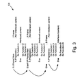
- Fig. 3 is an example video processing algorithm
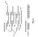
- Fig. 4 illustrates how the system of Fig. 1 may implement the algorithm of Fig. 3 ;
- Fig. 5 illustrates how various programs in Fig. 4 may be stored in a memory.
- Fig. 1 illustrates an example system 100.
- Example implementations of system 100 may include personal video recorders (PVRs) or digital versatile disc recorders (DVD-Rs), although the claimed invention is not limited in this regard.
- system 100 may be embodied within a general-purpose computer, a portable device, a consumer electronics device, or another electrical system.
- system 100 may be embodied in a single device, in some implementations certain components of system 100 may be remote and/or physically separated from other components of system 100.
- system 100 is illustrated as including discrete components, these components may be implemented in hardware, software/firmware, or some combination thereof. When implemented in hardware, some components of system 100 may be combined in a certain chip or device.
- System 100 may include a data source 110, a memory 120, a data processor 130, and a data destination 170.
- Source 110 may send data to memory 120, and the data in memory 120 may be processed by data processor 130.
- the processed data may be sent to destination 170.
- the data sent and operated upon may include media data (e.g., video information), but the claimed invention is not limited in this regard.
- Data processor 130 may process other types of data than media information consistent with the description herein.
- Source 110 may include a device that provides media information to the remainder of system 100.
- the media information provided by source 110 may include video information encoded in a format such as MPEG-1, MPEG-2, MPEG-4, H.264, Windows Media Video version 9 (WMV9) and Advanced Video System (AVS) formats.
- WMV9 Windows Media Video version 9
- AVS Advanced Video System
- source 110 may include a tuner to separate a stream or channel of video information (e.g., high definition (HD) MPEG-2 information) from other streams or channels of media information.
- source 110 may include a reader to read the media information from a storage medium.
- a reader may include an optical, magnetic, and/or electrical reader to extract the video information from a DVD, hard disk, semiconductor storage device, or other storage medium.
- source 110 may include receiver circuitry to receive the media information from a communication link (not shown). Such receiver in source 110 may be arranged to receive information from a wired, optical, or wireless transmission medium. The receiver in source 110 may, or may not, operate in conjunction with a tuner or other device to separate desired information from other received information.
- Memory 120 may receive media information from source 110 and store the media information. If instructed by data processor 130, memory 120 may provide processed media data to destination 170 and/or destination 170 may read such processed media data when triggered by data processor 130.
- Memory 120 may include random access memory (RAM) to facilitate rapid transfer and storage of data. Such RAM may be synchronous, asynchronous, double data rate (DDR), etc. according to the design parameters of system 100.
- RAM random access memory
- memory 120 may store instructions for use by data processor 130 and/or its components. Such instructions may be task-specific, and may be provided to data processor 130 when requested. Memory 120 may include one or more sets of such instructions that, when loaded by data processor 130, enable data processor 130 to perform a variety of processing tasks on the data (e.g., media or video data) received from source 110.
- data e.g., media or video data
- Data processor 130 may include a control processor 140, a number of low-level processors 150-1, 150-2, ..., 150-n (collectively "low-level processors 150"), and a direct memory access (DMA) 160.
- all of elements 130-160 may be located in the same chip or package.
- low level processors 150 and DMA 160 may be in one chip or package, while control processor 140 may be located in a separate chip or package. Other combinations and implementations are possible.
- Control processor 140 may include sufficient instruction memory to control and/or coordinate a relatively complex processing operation. In handling such a complex operation (e.g., decoding video information), control processor may both determine what resources are needed for the task (e.g., by parsing an algorithm such as a decoding algorithm) and allocate resources to the task (e.g., by configuring low-level processors 150 appropriately). In this latter, allocation function, control processor 140 may be arranged to load task-specific instructions from memory 120 into low-level processors 150.
- a complex operation e.g., decoding video information
- control processor may both determine what resources are needed for the task (e.g., by parsing an algorithm such as a decoding algorithm) and allocate resources to the task (e.g., by configuring low-level processors 150 appropriately). In this latter, allocation function, control processor 140 may be arranged to load task-specific instructions from memory 120 into low-level processors 150.
- control processor 140 may examine indicator data to determine what type of processing should be performed. Control processor 140 may then configure low-level processors 150 with appropriate instructions from memory 120 to process the data from source 110 that follows the indicator data. Control processor 140 may also assign certain ones of low-level processors 150 to process certain data and/or perform certain tasks in parallel. Control processor 140 may reconfigure low-level processors 150, as needed, based on newly received indicator data. This control scheme will be described in greater detail below.
- control processor 140 may handle the logical complexity and may configure low-level processors 150 "on the fly," if desired, to handle the amounts of data. To accomplish these functions, control processor 140 may have room in its instruction memory for more than about ten times the number of instructions (e.g., be at least ten times larger than) as low-level processors 150. In one implementation, control processor 140 may have about 32 kilobytes (KB) of instruction RAM, although the claimed invention is not limited in this regard.
- Low-level processors 150 may include a number of processors with smaller amounts of instruction memory (e.g., less than a tenth as much) than control processor 140. In one implementation, low-level processors 150 each may have about 1.5 kilobytes (KB) of instruction RAM, although the claimed invention is not limited in this regard. Because of the smaller amounts of instruction memory, each of low-level processors 150 may perform a task corresponding to a relatively small code size. Low-level processors 150 also may lack, for example, one or more of caches, deep pipelines, branch prediction, speculative execution, etc. The relatively small memory and relatively simple structure of low-level processors 150, however, may result in power and size savings relative to more complex processors. In some implementations, low-level processors 150 may be homogeneous in structure and capability, and in some implementations, low-level processors 150 may be heterogeneous in structure and/or capability.
- KB kilobytes
- low-level processors 150 may be interconnected in some implementations, for example, in a matrix-type arrangement where one of low-level processors 150 may be connected to one, two, three, or more others of low-level processors 150. In some implementations, there may be a single digit number of low-level processors 150 (e.g., four or eight), but in other implementations there may be a double-digit number of low-level processors 150 (e.g., 16, 20, 32, 40, etc.). Also, though low-level processors 150 will be described as executing a processing task, in some implementations each of low-level processors 150 may execute a sub-task in conjunction with one or more of low-level processors 150. Other architectural and processing flow variations are both possible and contemplated for low-level processors 150.
- low-level processors 150 may receive instructions from memory 120 and data to process using those instructions in based on direction from control processor 140. Depending on the instructions received, each of low-level processors 150 may be arranged to be a specific-purpose processor, with different processing tasks possible among the processors. Low-level processors 150 may be arranged to retrieve and process their respective data, possibly in parallel. Further, any one of low-level processors 150 may be reconfigured (e.g., receive different instructions) as often as upon completion of its current task. Control processor 140 may, however, re-use (i.e., not reconfigure) some of low-level processors 150 if they are already configured for tasks that need to be performed. Because of configuration of low-level processors 150 by control processor 140, data processor 130 may be referred to as a hierarchical processor.
- DMA 160 may read and/or write data from and/or to memory 120. In so doing, DMA 160 may facilitate control processor 140 reading indicator data from source 110. DMA 160 may also provide instruction data and data to be processed to low-level processors 150. DMA 160 also may control data flow among low-level processors 150. Although DMA 160 is illustrated as connected to memory 120 with a single connection, it should be understood that such merely shows bi-directional data transfer between DMA 160 and memory 120, and does not limit the claimed invention. In practice, one or more additional (e.g., control) connections may exist between DMA 160 and memory 120, even though not explicitly shown in Fig. 1 . This illustrative principle also applies to other connections shown in Fig. 1 .
- Data destination 170 may be arranged to store or output processed data (e.g., decoded media or video information).
- destination 170 may include an output interface to provide another system or another component of system 100 (not shown) access to the data processed by data processor 130.
- Such a physical output interface may be optical, electrical, wireless, etc., and may conform to one or more existing or later-developed interface specifications for transmitting and/or accessing data.
- destination 170 may include a storage device for storing the processed data.
- destination 170 may include a hard disk or flash memory to store information.
- destination 170 may include a writeable optical drive (e.g., DVD-RW, etc.) to transfer processed information to a portable storage medium.
- a display processor (not shown) may access the stored information in destination 170 for playback or some other purpose at a later time.
- destination 170 need not necessarily be separate or distinct from source 110 in some implementations.
- Decoded video information in some implementations, may be re-inserted (e.g., by back modulation in another channel) into a stream from which it was received.
- Fig. 2 is a flow chart illustrating a process 200 of operating on data. Although process 200 may be described with regard to system 100 for ease of explanation, the claimed invention is not limited in this regard. Processing may begin with control processor 140 reading indicator data from memory 120 and determining one or more tasks to be performed based on the indicator data [act 210]. Control processor 140 may make such determination using instructions (e.g., forming an algorithm) resident in its instruction memory. In one example, described in greater detail below, control processor 140 may execute a decoding algorithm for video data, and the indicator data used may be, for example, what type of encoding a particular frame of video data has.
- instructions e.g., forming an algorithm
- control processor 140 may instruct DMA 160 to access appropriate instructions (e.g., micro-code program(s)) in memory 120 and pass them along to low-level processors 150.
- control processor 140 may instruct low-level processors 150 to obtain the instructions from memory 120 via DMA 160. As long as the indicator data precedes other data to be processed, control processor 140 may load instructions into low-level processors 150 with relatively low delay or latency.
- Low-level processors 150 may execute the instructions to perform the one or more tasks determined by control processor 140 [act 230]. Such execution may begin shortly after loading the instructions, perhaps after minor configurations (e.g., where to retrieve data in memory 120) are made to low-level processors 150. As part of act 230, or an earlier act, control processor 140 or low-level processors 150 may program DMA 160 to deliver and accept data to and from low-level processors 150 during their processing tasks. Although a single low-level processor 150 may perform one computing task, in some implementations two or more low-level processors 150 may cooperate to perform one task. Also, low-level processors 150 may perform their respective task(s) or portions of such task(s) in parallel in some implementations.
- Low-level processors 150 may transfer data to and from memory 120 via DMA 160 as appropriate for their respective processing task(s) [act 240]. When such processing is complete, the processed data may be transferred to memory 120 for buffering and/or transfer to destination 170.
- Acts 210-240 may be repeated as appropriate for successive computing tasks. As described above, control processor 140 may perform and/or coordinate acts 210 and 220, and low-level processors 150 may perform and/or coordinate acts 230 and 240. Repetition of acts 210-240 may depend on when indicator data is received by memory 120. If, for example, the next piece of indicator data (e.g., indicating the next task or set of tasks) is not received until after low-level processors 150 have processed the data, control processor 140 may not repeat act 210 until after act 240, as illustrated by the solid arrow in Fig. 2 .
- indicator data e.g., indicating the next task or set of tasks
- control processor 140 may repeat act 210 after act 220, as illustrated by the dashed arrow in Fig. 2 .
- control processor 140 may finish loading instructions into some of low-level processors 150, and it may determine tasks and load instructions in acts 210 and 220 while the low-level processors 150 are executing in acts 230 and 240.
- Other processing flows between control processor 140 and low-level processors 150 are possible consistent with the description herein.
- system 100 and process 200 may be amenable to decoding video information, as described below, the claimed invention should not be limited thereto. Further, system 100 and process 200 may be amenable to much more complicated algorithms, whether video decoding or other types, than are discussed below.
- Fig. 3 illustrates an example video processing algorithm 300.
- Algorithm 300 may perform one or more of Functions A-G to decode a frame of video information, depending on whether the frame is an intracoded (I) picture, a predicted (P) picture, or a bi-directionally predicted (B) picture, and depending on whether the particular I, P, or B picture includes interlaced or progressively scanned video information.
- This type of frame (e.g., B frame) and mode of video (e.g., interlaced) information may be one example of indicator data, because it indicates what processing tasks should be performed on the remainder of the video data in the frame.
- algorithm 300 determines that Functions D and G be performed to decode such a frame of video information.
- the arrows in Fig. 3 illustrate the logical steps taken to make a determination of which functions to perform.
- Functions D and G may represent to distinct computational tasks necessary to decode an interlaced B frame of video data.
- Control processor 140 may then load Program 2 [act 220] into one or more of low-level processors 150 and cause it to be executed. Based on the complexity of Program 2, control processor 140 may load corresponding instructions into a single one of low-level processors 150 or into multiple ones of low-level processors 150. Control processor 140 may determine whether to distribute Program 2 over multiple low-level processors 150, or such may be pre-determined and reflected in, for example, how Program 2 is stored in memory 120. Once control processor 140 has loaded Program 2, it may perform acts 21 and 220 again if the indicator data (e.g., frame type and/or mode) is available for another frame of video data.
- the indicator data e.g., frame type and/or mode
- Low-level processor(s) 150 may then perform Functions D and G, the first and second parts of program 2 [acts 230/240].
- one low-level processor e.g., 150-1
- one low-level processor e.g., 150-1
- one low-level processor e.g., 150-1
- one low-level processor e.g., 150-2
- two or more low-level processors 150 may cooperate to perform at least one of Functions D and G, such as Function G. Other implementations are possible consistent with the description herein.
- Fig. 5 illustrates how Programs 0-5 may be stored in memory 120.
- Structure 500 may include a data structure such as a linked list, an array, etc. within memory 120.
- Programs 0-5 may reside at certain addresses in structure 500, notionally illustrated by rows within the structure.
- the same version of a program (e.g., Program 2) is executed by any of low-level processors 150.
- the dotted lines defining columns within structure 500 denote the possibility of different treatment of a program (e.g., Program 2) for different ones of low-level processors 150.
- a program e.g., Program 2
- a program may be split into a number of portions (e.g., three in Fig. 5 , although this should not limit the claimed invention) for different low-level processors (e.g., 150-1 to 150-3) to execute.
- a first part of Program 2 may be instructions to perform Function D
- a second (and possible third) portion of Program 2 may be instructions to perform Function G.
- different ones of low-level processors 150 may load subtly different versions of a program (e.g., Program 2 or a portion thereof) to aid in addressing, data transfer, etc.
- system 100 may include a possibly lower-performance (e.g., lower power) control processor 140 that can handle the logical complexity of an algorithm and many lower-complexity (e.g., smaller and/or lower power) low-level processors 150 to handle the computational load of the algorithm.
- system 100 may consume less power than would be otherwise possible for the same computational operation (e.g., video decoding). Both high performance and low power usage may be obtained by system 100, because in video decompression, for example, the indicator data (e.g., detailed information about what processing tasks will be upcoming) is transmitted ahead of the other data.
- control processor 140 may customize and/or reconfigure the remainder of data processor 130 on the fly to perform just that upcoming task.
- the hierarchical processing scheme described herein is not limited to video data. Rather, it may be applied to any data for which indicator data (e.g., data which indicates a future processing task) is available with which to configure low-level processors 150, or another processor or logic that is programmable on the fly.
- indicator data e.g., data which indicates a future processing task
- memory 120 may include multiple devices.
- the data to be processed may be stored in a relatively large RAM, while the instructions for low-level processors 150 may be stored in a smaller RAM, a dedicated read-only memory (ROM), or some other separate storage device.
- control processor 140 handled the algorithmic complexity and low-level processors 150 handled the data processing, such rigid separation of complexity and processing need not always occur.
- control processor 140 may, in some instances, process data
- low-level processors 150 may, in some instances, handle limited logical parsing and/or decision making. In such hybrid schemes, however, it mat still be desirable for low-level processors 150 to process as much data as practical and for control processor 140 to handle as much of the algorithmic complexity as practical.
- decoding of video information has been described as one implementation, other functions are possible in other implementations.
- system 100 may be arranged to encode media information, to render media information, to model physical phenomena, or to perform other, relatively complex numerical operations that may involve processing a large amount of data.
- the acts in Fig. 2 need not be implemented in the order shown; nor do all of the acts necessarily need to be performed. Also, those acts that are not dependent on other acts may be performed in parallel with the other acts. Further, at least some of the acts in this figure may be implemented as instructions, or groups of instructions, implemented in a machine-readable medium.
Landscapes
- Engineering & Computer Science (AREA)
- Computer Hardware Design (AREA)
- Theoretical Computer Science (AREA)
- Physics & Mathematics (AREA)
- General Engineering & Computer Science (AREA)
- General Physics & Mathematics (AREA)
- Multimedia (AREA)
- Signal Processing (AREA)
- Compression Or Coding Systems Of Tv Signals (AREA)
- Image Processing (AREA)
- Multi Processors (AREA)
- Two-Way Televisions, Distribution Of Moving Picture Or The Like (AREA)
Claims (9)
- System (100) zum Decodieren von Videoinformationen, wobei das System anpassbar ist abhängig von Gattungsinformationen, welche Frames von Videoinformationen beschreiben, dadurchgekennzeichnet, dass das System folgendes umfasst:einen Speicher (120) zum Speichern von Frames von Videoinformationen, Gattungsinformationen, welche die Frames von Videoinformationen beschreiben, und Befehlen zum Decodieren der Frames von Videoinformationen;eine Mehrzahl von Prozessoren (150), die jeweils einen Befehlsspeicher zum Speichern bestimmter Befehle zum Decodieren von Frames von Videoinformationen aufweisen, wobei jeder Prozessor (150) der genannten Mehrzahl von Prozessoren (150) so angeordnet ist, dass die bestimmten Anweisungen ausgeführt werden, die in dem Befehlsspeicher gespeichert sind, um einen Frame der Videoinformationen zu decodieren;einen Steuerungsprozessor (140) zum Bestimmen einer Teilmenge der Befehle, die benötigt werden zum Verarbeiten eines bestimmten Frames der Videoinformationen, anhand der Gattungsinformationen, welche den bestimmten Frame beschreiben, und um zu bewirken, dass die Teilmenge der Befehle in dem Befehlsspeicher mindestens eines Prozessors der Mehrzahl von Prozessoren (150) zur Ausführung dadurchgespeichert wird.
- System nach Anspruch 1, wobei der Befehlsspeicher jedes Prozessors (150) der genannten Mehrzahl von Prozessoren (150) eine erste Größe aufweist; und
wobei der Steuerungsprozessor (140) einen Befehlsspeicher einer zweiten Größe aufweist, der mindestens zehnmal so groß ist wie die erste Größe. - System nach Anspruch 1, wobei das System ferner folgendes umfasst:eine Vorrichtung für direkten Speicherzugriff (DMA) (160), die mit dem Speicher, der Mehrzahl von Prozessoren (150) und dem Steuerungsprozessor (140) verbundenist, um die Übertragung von Frames von Videoinformationen, der Gattungsinformationen und der Befehle zu koordinieren.
- System nach Anspruch 1, wobei die Gattungsinformationen erste Informationen aufweisen, welche eine Frame-Art der Videoinformationen anzeigen, oder zweite Informationen, welche eine Abtastart der Videoinformationen anzeigen.
- Verfahren zum Decodieren von Videoinformationen in einem System, das anpassbar ist abhängig von Gattungsinformationen, welche Frames von Videoinformationen beschreiben, wobei das Verfahren gekennzeichnet ist durch:das Bestimmen durch einen Steuerungsprozessor (140) einer Teilmenge von Befehlen, die in einem Speicher (120) gespeichert sind, für die Verarbeitung eines bestimmten Frames von Videoinformationen auf der Basis der in dem Speicher gespeicherten Gattungsinformationen, welche den jeweiligen Frame beschreiben, und wobei die Teilmenge von Befehlen in einem Befehlsspeicher mindestens einen Prozessors einer Mehrzahl von Prozessoren (150) gespeichert wird;das Ausführen durch den mindestens einen Prozessor der Mehrzahl von Prozessoren (150) der Teilmenge von Befehlen, die in dem Befehlsspeicher gespeichert sind, so dass der Frame der Videoinformationen decodiert wird.
- Verfahren nach Anspruch 5, wobei die Gattungsinformationen mindestens eine Frame-Art der Videoinformationen aufweisen.
- Verfahren nach Anspruch 5, wobei die Gattungsinformationen mindestens einen Anzeigemodus der Videoinformationen aufweisen.
- Verfahren nach Anspruch 5, wobei das Verfahren ferner folgendes umfasst:das Bestimmen anhand der Gattungsinformationen durch den Steuerungsprozessor (140) und nach dem genannten Speichern einer weiteren auszuführenden Decodierungsaufgabe; unddas Speichern zweiter Befehle zum Ausführen einer weiteren Decodierungsaufgabe in einem Befehlsspeicher in einem Prozessor der Mehrzahl von Prozessoren (150).
- Verfahren nach Anspruch 8, wobei das Verfahren ferner folgendes umfasst:das Ausführen durch einen Prozessor der Mehrzahl von Prozessoren (150) der zweiten Befehle in dem Befehlsspeicher zum Decodieren eines anderen Frames von Videoinformationen.
Applications Claiming Priority (2)
| Application Number | Priority Date | Filing Date | Title |
|---|---|---|---|
| US10/850,095 US20050262311A1 (en) | 2004-05-20 | 2004-05-20 | Hierarchical processor architecture for video processing |
| PCT/US2005/015130 WO2005116853A1 (en) | 2004-05-20 | 2005-04-29 | Hierarchical processor architecture for video processing |
Publications (2)
| Publication Number | Publication Date |
|---|---|
| EP1747513A1 EP1747513A1 (de) | 2007-01-31 |
| EP1747513B1 true EP1747513B1 (de) | 2010-03-31 |
Family
ID=34967606
Family Applications (1)
| Application Number | Title | Priority Date | Filing Date |
|---|---|---|---|
| EP05741218A Expired - Lifetime EP1747513B1 (de) | 2004-05-20 | 2005-04-29 | Hierarchische prozessorarchitektur zur videoverarbeitung |
Country Status (8)
| Country | Link |
|---|---|
| US (1) | US20050262311A1 (de) |
| EP (1) | EP1747513B1 (de) |
| JP (1) | JP4964774B2 (de) |
| CN (1) | CN100555322C (de) |
| AT (1) | ATE463011T1 (de) |
| DE (1) | DE602005020271D1 (de) |
| TW (1) | TWI308727B (de) |
| WO (1) | WO2005116853A1 (de) |
Families Citing this family (9)
| Publication number | Priority date | Publication date | Assignee | Title |
|---|---|---|---|---|
| US7965898B2 (en) * | 2005-10-28 | 2011-06-21 | Nvidia Corporation | Accelerating video decoding using multiple processors |
| JP2010282429A (ja) * | 2009-06-04 | 2010-12-16 | Canon Inc | 画像処理装置及びその制御方法 |
| US9013750B2 (en) * | 2009-06-25 | 2015-04-21 | Canon Kabushiki Kaisha | Image processing for processing image data in correspondence with each pixel of an image |
| US8976411B2 (en) * | 2009-07-01 | 2015-03-10 | Canon Kabushiki Kaisha | Image processing in correspondence with each pixel of an image |
| US9635218B2 (en) | 2009-07-03 | 2017-04-25 | Canon Kabushiki Kaisha | Image processing based on a pixel value in image data |
| US9880848B2 (en) * | 2010-06-11 | 2018-01-30 | Advanced Micro Devices, Inc. | Processor support for hardware transactional memory |
| JP5671635B2 (ja) * | 2014-01-07 | 2015-02-18 | キヤノン株式会社 | 画像処理装置及びその制御方法 |
| CN104023202B (zh) * | 2014-03-18 | 2018-04-27 | 山东大学 | 高清视频处理系统 |
| JP6575350B2 (ja) * | 2015-12-24 | 2019-09-18 | ブラザー工業株式会社 | レーザ加工装置 |
Family Cites Families (17)
| Publication number | Priority date | Publication date | Assignee | Title |
|---|---|---|---|---|
| US4243987A (en) * | 1978-06-27 | 1981-01-06 | Xerox Corporation | Display processor for producing video signals from digitally encoded data to create an alphanumeric display |
| US5016876A (en) * | 1988-10-14 | 1991-05-21 | Williams Electronics Games, Inc. | Video display co-processor for use in a video game |
| US4965793A (en) * | 1989-02-03 | 1990-10-23 | Digital Equipment Corporation | Method and apparatus for interfacing a system control unit for a multi-processor |
| US5522083A (en) * | 1989-11-17 | 1996-05-28 | Texas Instruments Incorporated | Reconfigurable multi-processor operating in SIMD mode with one processor fetching instructions for use by remaining processors |
| JPH07105158A (ja) * | 1993-10-05 | 1995-04-21 | Matsushita Electric Ind Co Ltd | プログラムローダ |
| JPH07221996A (ja) * | 1994-02-01 | 1995-08-18 | Canon Inc | 画像処理方法およびその装置 |
| JPH0844678A (ja) * | 1994-07-29 | 1996-02-16 | Canon Inc | 画像処理装置及びシステム |
| KR100213048B1 (ko) * | 1995-09-29 | 1999-08-02 | 윤종용 | 아날로그와 디지탈 비디오 모드를 갖는 수신기와 그 수신방법 |
| US6237029B1 (en) * | 1996-02-26 | 2001-05-22 | Argosystems, Inc. | Method and apparatus for adaptable digital protocol processing |
| TW376642B (en) * | 1996-05-07 | 1999-12-11 | Matsushita Electric Industrial Co Ltd | Video signal processing apparatus |
| JPH1028245A (ja) * | 1996-05-07 | 1998-01-27 | Matsushita Electric Ind Co Ltd | 映像信号処理装置 |
| JPH1091594A (ja) * | 1996-09-13 | 1998-04-10 | Hitachi Ltd | マルチプロセッサデータ処理装置およびその方法 |
| FI107842B (fi) * | 1997-09-23 | 2001-10-15 | Nokia Networks Oy | Adaptiivinen prosessorijärjestelmä |
| JP2001312480A (ja) * | 2000-05-01 | 2001-11-09 | Nec Corp | マルチプロセッサシステム |
| JP4640880B2 (ja) * | 2000-07-14 | 2011-03-02 | 国立大学法人東京工業大学 | マイクロプロセッサシステム |
| US7636125B2 (en) * | 2002-10-22 | 2009-12-22 | Broadcom Corporation | Filter module for a video decoding system |
| US7499495B2 (en) * | 2003-07-18 | 2009-03-03 | Microsoft Corporation | Extended range motion vectors |
-
2004
- 2004-05-20 US US10/850,095 patent/US20050262311A1/en not_active Abandoned
-
2005
- 2005-04-29 DE DE602005020271T patent/DE602005020271D1/de not_active Expired - Lifetime
- 2005-04-29 WO PCT/US2005/015130 patent/WO2005116853A1/en not_active Ceased
- 2005-04-29 AT AT05741218T patent/ATE463011T1/de not_active IP Right Cessation
- 2005-04-29 EP EP05741218A patent/EP1747513B1/de not_active Expired - Lifetime
- 2005-04-29 JP JP2007527262A patent/JP4964774B2/ja not_active Expired - Fee Related
- 2005-05-05 TW TW094114512A patent/TWI308727B/zh active
- 2005-05-20 CN CNB200510075898XA patent/CN100555322C/zh not_active Expired - Fee Related
Also Published As
| Publication number | Publication date |
|---|---|
| CN1716312A (zh) | 2006-01-04 |
| US20050262311A1 (en) | 2005-11-24 |
| CN100555322C (zh) | 2009-10-28 |
| DE602005020271D1 (de) | 2010-05-12 |
| TW200620152A (en) | 2006-06-16 |
| ATE463011T1 (de) | 2010-04-15 |
| TWI308727B (en) | 2009-04-11 |
| JP4964774B2 (ja) | 2012-07-04 |
| JP2007538334A (ja) | 2007-12-27 |
| EP1747513A1 (de) | 2007-01-31 |
| WO2005116853A1 (en) | 2005-12-08 |
Similar Documents
| Publication | Publication Date | Title |
|---|---|---|
| US9251553B2 (en) | Dual control of a dynamically reconfigurable pipelined pre-processor | |
| US8754893B2 (en) | Apparatus and method for selectable hardware accelerators | |
| EP2891054B1 (de) | Verfahren und systeme zur stromverwaltung in einem mustererkennungsverarbeitungssystem | |
| JP4664406B2 (ja) | 動画像復号化装置、半導体装置、映像機器および動画像復号化方法 | |
| US11638041B2 (en) | Multiple transcode engine systems and methods | |
| US20080170611A1 (en) | Configurable functional multi-processing architecture for video processing | |
| WO2010080645A2 (en) | Memory subsystem | |
| US20050262311A1 (en) | Hierarchical processor architecture for video processing | |
| US20090006437A1 (en) | Multi-Processor | |
| US20100053181A1 (en) | Method and device of processing video | |
| US8443413B2 (en) | Low-latency multichannel video port aggregator | |
| JP4865662B2 (ja) | エントロピー符号化装置、エントロピー符号化方法およびコンピュータプログラム | |
| CN216751965U (zh) | 一种基于fpga的arinc818视频数据压缩与解压缩处理装置 | |
| US8854382B2 (en) | Multi-function encoder and decoder devices, and methods thereof | |
| KR100860160B1 (ko) | 비디오 처리를 위한 계층 프로세서 아키텍처 | |
| JP3738802B2 (ja) | 情報処理システム | |
| Pinto et al. | Hiveflex-video vsp1: Video signal processing architecture for video coding and post-processing | |
| US8060702B2 (en) | Information reproducing apparatus and information reproducing method | |
| US7729591B2 (en) | Data processing apparatus, reproduction apparatus, data processing system, reproduction method, program, and storage medium | |
| US8261034B1 (en) | Memory system for cascading region-based filters | |
| US20080091438A1 (en) | Audio signal decoder and resource access control method | |
| KR101652694B1 (ko) | 적응적 연산 장치 및 적응적 연산 장치 작동 방법 | |
| US20130094586A1 (en) | Direct Memory Access With On-The-Fly Generation of Frame Information For Unrestricted Motion Vectors | |
| US20060007235A1 (en) | Method of accessing frame data and data accessing device thereof | |
| Wang et al. | Unified VLSI architecture of motion vector and boundary strength parameter decoder for 8K UHDTV HEVC decoder |
Legal Events
| Date | Code | Title | Description |
|---|---|---|---|
| PUAI | Public reference made under article 153(3) epc to a published international application that has entered the european phase |
Free format text: ORIGINAL CODE: 0009012 |
|
| 17P | Request for examination filed |
Effective date: 20061012 |
|
| AK | Designated contracting states |
Kind code of ref document: A1 Designated state(s): AT BE BG CH CY CZ DE DK EE ES FI FR GB GR HU IE IS IT LI LT LU MC NL PL PT RO SE SI SK TR |
|
| 17Q | First examination report despatched |
Effective date: 20070302 |
|
| DAX | Request for extension of the european patent (deleted) | ||
| GRAP | Despatch of communication of intention to grant a patent |
Free format text: ORIGINAL CODE: EPIDOSNIGR1 |
|
| GRAS | Grant fee paid |
Free format text: ORIGINAL CODE: EPIDOSNIGR3 |
|
| GRAA | (expected) grant |
Free format text: ORIGINAL CODE: 0009210 |
|
| AK | Designated contracting states |
Kind code of ref document: B1 Designated state(s): AT BE BG CH CY CZ DE DK EE ES FI FR GB GR HU IE IS IT LI LT LU MC NL PL PT RO SE SI SK TR |
|
| REG | Reference to a national code |
Ref country code: GB Ref legal event code: FG4D Ref country code: CH Ref legal event code: EP |
|
| REG | Reference to a national code |
Ref country code: IE Ref legal event code: FG4D |
|
| REF | Corresponds to: |
Ref document number: 602005020271 Country of ref document: DE Date of ref document: 20100512 Kind code of ref document: P |
|
| REG | Reference to a national code |
Ref country code: NL Ref legal event code: VDEP Effective date: 20100331 |
|
| PG25 | Lapsed in a contracting state [announced via postgrant information from national office to epo] |
Ref country code: LT Free format text: LAPSE BECAUSE OF FAILURE TO SUBMIT A TRANSLATION OF THE DESCRIPTION OR TO PAY THE FEE WITHIN THE PRESCRIBED TIME-LIMIT Effective date: 20100331 |
|
| LTIE | Lt: invalidation of european patent or patent extension |
Effective date: 20100331 |
|
| PG25 | Lapsed in a contracting state [announced via postgrant information from national office to epo] |
Ref country code: PL Free format text: LAPSE BECAUSE OF FAILURE TO SUBMIT A TRANSLATION OF THE DESCRIPTION OR TO PAY THE FEE WITHIN THE PRESCRIBED TIME-LIMIT Effective date: 20100331 Ref country code: FI Free format text: LAPSE BECAUSE OF FAILURE TO SUBMIT A TRANSLATION OF THE DESCRIPTION OR TO PAY THE FEE WITHIN THE PRESCRIBED TIME-LIMIT Effective date: 20100331 Ref country code: AT Free format text: LAPSE BECAUSE OF FAILURE TO SUBMIT A TRANSLATION OF THE DESCRIPTION OR TO PAY THE FEE WITHIN THE PRESCRIBED TIME-LIMIT Effective date: 20100331 Ref country code: SI Free format text: LAPSE BECAUSE OF FAILURE TO SUBMIT A TRANSLATION OF THE DESCRIPTION OR TO PAY THE FEE WITHIN THE PRESCRIBED TIME-LIMIT Effective date: 20100331 |
|
| PG25 | Lapsed in a contracting state [announced via postgrant information from national office to epo] |
Ref country code: RO Free format text: LAPSE BECAUSE OF FAILURE TO SUBMIT A TRANSLATION OF THE DESCRIPTION OR TO PAY THE FEE WITHIN THE PRESCRIBED TIME-LIMIT Effective date: 20100331 Ref country code: EE Free format text: LAPSE BECAUSE OF FAILURE TO SUBMIT A TRANSLATION OF THE DESCRIPTION OR TO PAY THE FEE WITHIN THE PRESCRIBED TIME-LIMIT Effective date: 20100331 Ref country code: CY Free format text: LAPSE BECAUSE OF FAILURE TO SUBMIT A TRANSLATION OF THE DESCRIPTION OR TO PAY THE FEE WITHIN THE PRESCRIBED TIME-LIMIT Effective date: 20100331 Ref country code: BE Free format text: LAPSE BECAUSE OF FAILURE TO SUBMIT A TRANSLATION OF THE DESCRIPTION OR TO PAY THE FEE WITHIN THE PRESCRIBED TIME-LIMIT Effective date: 20100331 Ref country code: SE Free format text: LAPSE BECAUSE OF FAILURE TO SUBMIT A TRANSLATION OF THE DESCRIPTION OR TO PAY THE FEE WITHIN THE PRESCRIBED TIME-LIMIT Effective date: 20100331 Ref country code: ES Free format text: LAPSE BECAUSE OF FAILURE TO SUBMIT A TRANSLATION OF THE DESCRIPTION OR TO PAY THE FEE WITHIN THE PRESCRIBED TIME-LIMIT Effective date: 20100712 Ref country code: NL Free format text: LAPSE BECAUSE OF FAILURE TO SUBMIT A TRANSLATION OF THE DESCRIPTION OR TO PAY THE FEE WITHIN THE PRESCRIBED TIME-LIMIT Effective date: 20100331 |
|
| PG25 | Lapsed in a contracting state [announced via postgrant information from national office to epo] |
Ref country code: CZ Free format text: LAPSE BECAUSE OF FAILURE TO SUBMIT A TRANSLATION OF THE DESCRIPTION OR TO PAY THE FEE WITHIN THE PRESCRIBED TIME-LIMIT Effective date: 20100331 Ref country code: SK Free format text: LAPSE BECAUSE OF FAILURE TO SUBMIT A TRANSLATION OF THE DESCRIPTION OR TO PAY THE FEE WITHIN THE PRESCRIBED TIME-LIMIT Effective date: 20100331 Ref country code: MC Free format text: LAPSE BECAUSE OF NON-PAYMENT OF DUE FEES Effective date: 20100430 Ref country code: IS Free format text: LAPSE BECAUSE OF FAILURE TO SUBMIT A TRANSLATION OF THE DESCRIPTION OR TO PAY THE FEE WITHIN THE PRESCRIBED TIME-LIMIT Effective date: 20100731 |
|
| REG | Reference to a national code |
Ref country code: CH Ref legal event code: PL |
|
| PG25 | Lapsed in a contracting state [announced via postgrant information from national office to epo] |
Ref country code: DK Free format text: LAPSE BECAUSE OF FAILURE TO SUBMIT A TRANSLATION OF THE DESCRIPTION OR TO PAY THE FEE WITHIN THE PRESCRIBED TIME-LIMIT Effective date: 20100331 Ref country code: PT Free format text: LAPSE BECAUSE OF FAILURE TO SUBMIT A TRANSLATION OF THE DESCRIPTION OR TO PAY THE FEE WITHIN THE PRESCRIBED TIME-LIMIT Effective date: 20100802 Ref country code: IE Free format text: LAPSE BECAUSE OF NON-PAYMENT OF DUE FEES Effective date: 20100429 |
|
| PLBE | No opposition filed within time limit |
Free format text: ORIGINAL CODE: 0009261 |
|
| STAA | Information on the status of an ep patent application or granted ep patent |
Free format text: STATUS: NO OPPOSITION FILED WITHIN TIME LIMIT |
|
| PG25 | Lapsed in a contracting state [announced via postgrant information from national office to epo] |
Ref country code: CH Free format text: LAPSE BECAUSE OF NON-PAYMENT OF DUE FEES Effective date: 20100430 Ref country code: LI Free format text: LAPSE BECAUSE OF NON-PAYMENT OF DUE FEES Effective date: 20100430 |
|
| 26N | No opposition filed |
Effective date: 20110104 |
|
| PG25 | Lapsed in a contracting state [announced via postgrant information from national office to epo] |
Ref country code: IT Free format text: LAPSE BECAUSE OF FAILURE TO SUBMIT A TRANSLATION OF THE DESCRIPTION OR TO PAY THE FEE WITHIN THE PRESCRIBED TIME-LIMIT Effective date: 20100331 |
|
| REG | Reference to a national code |
Ref country code: FR Ref legal event code: ST Effective date: 20111125 |
|
| PG25 | Lapsed in a contracting state [announced via postgrant information from national office to epo] |
Ref country code: FR Free format text: LAPSE BECAUSE OF NON-PAYMENT OF DUE FEES Effective date: 20100531 |
|
| PG25 | Lapsed in a contracting state [announced via postgrant information from national office to epo] |
Ref country code: HU Free format text: LAPSE BECAUSE OF FAILURE TO SUBMIT A TRANSLATION OF THE DESCRIPTION OR TO PAY THE FEE WITHIN THE PRESCRIBED TIME-LIMIT Effective date: 20101001 Ref country code: LU Free format text: LAPSE BECAUSE OF NON-PAYMENT OF DUE FEES Effective date: 20100429 Ref country code: BG Free format text: LAPSE BECAUSE OF FAILURE TO SUBMIT A TRANSLATION OF THE DESCRIPTION OR TO PAY THE FEE WITHIN THE PRESCRIBED TIME-LIMIT Effective date: 20100331 |
|
| PG25 | Lapsed in a contracting state [announced via postgrant information from national office to epo] |
Ref country code: TR Free format text: LAPSE BECAUSE OF FAILURE TO SUBMIT A TRANSLATION OF THE DESCRIPTION OR TO PAY THE FEE WITHIN THE PRESCRIBED TIME-LIMIT Effective date: 20100331 |
|
| PG25 | Lapsed in a contracting state [announced via postgrant information from national office to epo] |
Ref country code: BG Free format text: LAPSE BECAUSE OF FAILURE TO SUBMIT A TRANSLATION OF THE DESCRIPTION OR TO PAY THE FEE WITHIN THE PRESCRIBED TIME-LIMIT Effective date: 20100630 |
|
| PG25 | Lapsed in a contracting state [announced via postgrant information from national office to epo] |
Ref country code: GR Free format text: LAPSE BECAUSE OF FAILURE TO SUBMIT A TRANSLATION OF THE DESCRIPTION OR TO PAY THE FEE WITHIN THE PRESCRIBED TIME-LIMIT Effective date: 20100331 |
|
| PGFP | Annual fee paid to national office [announced via postgrant information from national office to epo] |
Ref country code: DE Payment date: 20160426 Year of fee payment: 12 |
|
| PGFP | Annual fee paid to national office [announced via postgrant information from national office to epo] |
Ref country code: GB Payment date: 20170426 Year of fee payment: 13 |
|
| REG | Reference to a national code |
Ref country code: DE Ref legal event code: R119 Ref document number: 602005020271 Country of ref document: DE |
|
| PG25 | Lapsed in a contracting state [announced via postgrant information from national office to epo] |
Ref country code: DE Free format text: LAPSE BECAUSE OF NON-PAYMENT OF DUE FEES Effective date: 20171103 |
|
| GBPC | Gb: european patent ceased through non-payment of renewal fee |
Effective date: 20180429 |
|
| PG25 | Lapsed in a contracting state [announced via postgrant information from national office to epo] |
Ref country code: GB Free format text: LAPSE BECAUSE OF NON-PAYMENT OF DUE FEES Effective date: 20180429 |