EP1746564A2 - Method of driving a plasma display apparatus - Google Patents
Method of driving a plasma display apparatus Download PDFInfo
- Publication number
- EP1746564A2 EP1746564A2 EP06122084A EP06122084A EP1746564A2 EP 1746564 A2 EP1746564 A2 EP 1746564A2 EP 06122084 A EP06122084 A EP 06122084A EP 06122084 A EP06122084 A EP 06122084A EP 1746564 A2 EP1746564 A2 EP 1746564A2
- Authority
- EP
- European Patent Office
- Prior art keywords
- light emission
- grayscale
- pulses
- display apparatus
- brightness
- Prior art date
- Legal status (The legal status is an assumption and is not a legal conclusion. Google has not performed a legal analysis and makes no representation as to the accuracy of the status listed.)
- Withdrawn
Links
Images







Classifications
-
- G—PHYSICS
- G09—EDUCATION; CRYPTOGRAPHY; DISPLAY; ADVERTISING; SEALS
- G09G—ARRANGEMENTS OR CIRCUITS FOR CONTROL OF INDICATING DEVICES USING STATIC MEANS TO PRESENT VARIABLE INFORMATION
- G09G3/00—Control arrangements or circuits, of interest only in connection with visual indicators other than cathode-ray tubes
- G09G3/20—Control arrangements or circuits, of interest only in connection with visual indicators other than cathode-ray tubes for presentation of an assembly of a number of characters, e.g. a page, by composing the assembly by combination of individual elements arranged in a matrix no fixed position being assigned to or needed to be assigned to the individual characters or partial characters
- G09G3/2007—Display of intermediate tones
- G09G3/2059—Display of intermediate tones using error diffusion
-
- G—PHYSICS
- G09—EDUCATION; CRYPTOGRAPHY; DISPLAY; ADVERTISING; SEALS
- G09G—ARRANGEMENTS OR CIRCUITS FOR CONTROL OF INDICATING DEVICES USING STATIC MEANS TO PRESENT VARIABLE INFORMATION
- G09G3/00—Control arrangements or circuits, of interest only in connection with visual indicators other than cathode-ray tubes
- G09G3/20—Control arrangements or circuits, of interest only in connection with visual indicators other than cathode-ray tubes for presentation of an assembly of a number of characters, e.g. a page, by composing the assembly by combination of individual elements arranged in a matrix no fixed position being assigned to or needed to be assigned to the individual characters or partial characters
- G09G3/22—Control arrangements or circuits, of interest only in connection with visual indicators other than cathode-ray tubes for presentation of an assembly of a number of characters, e.g. a page, by composing the assembly by combination of individual elements arranged in a matrix no fixed position being assigned to or needed to be assigned to the individual characters or partial characters using controlled light sources
- G09G3/28—Control arrangements or circuits, of interest only in connection with visual indicators other than cathode-ray tubes for presentation of an assembly of a number of characters, e.g. a page, by composing the assembly by combination of individual elements arranged in a matrix no fixed position being assigned to or needed to be assigned to the individual characters or partial characters using controlled light sources using luminous gas-discharge panels, e.g. plasma panels
- G09G3/288—Control arrangements or circuits, of interest only in connection with visual indicators other than cathode-ray tubes for presentation of an assembly of a number of characters, e.g. a page, by composing the assembly by combination of individual elements arranged in a matrix no fixed position being assigned to or needed to be assigned to the individual characters or partial characters using controlled light sources using luminous gas-discharge panels, e.g. plasma panels using AC panels
- G09G3/291—Control arrangements or circuits, of interest only in connection with visual indicators other than cathode-ray tubes for presentation of an assembly of a number of characters, e.g. a page, by composing the assembly by combination of individual elements arranged in a matrix no fixed position being assigned to or needed to be assigned to the individual characters or partial characters using controlled light sources using luminous gas-discharge panels, e.g. plasma panels using AC panels controlling the gas discharge to control a cell condition, e.g. by means of specific pulse shapes
-
- G—PHYSICS
- G09—EDUCATION; CRYPTOGRAPHY; DISPLAY; ADVERTISING; SEALS
- G09G—ARRANGEMENTS OR CIRCUITS FOR CONTROL OF INDICATING DEVICES USING STATIC MEANS TO PRESENT VARIABLE INFORMATION
- G09G3/00—Control arrangements or circuits, of interest only in connection with visual indicators other than cathode-ray tubes
- G09G3/20—Control arrangements or circuits, of interest only in connection with visual indicators other than cathode-ray tubes for presentation of an assembly of a number of characters, e.g. a page, by composing the assembly by combination of individual elements arranged in a matrix no fixed position being assigned to or needed to be assigned to the individual characters or partial characters
- G09G3/2007—Display of intermediate tones
- G09G3/2018—Display of intermediate tones by time modulation using two or more time intervals
- G09G3/2022—Display of intermediate tones by time modulation using two or more time intervals using sub-frames
-
- G—PHYSICS
- G09—EDUCATION; CRYPTOGRAPHY; DISPLAY; ADVERTISING; SEALS
- G09G—ARRANGEMENTS OR CIRCUITS FOR CONTROL OF INDICATING DEVICES USING STATIC MEANS TO PRESENT VARIABLE INFORMATION
- G09G3/00—Control arrangements or circuits, of interest only in connection with visual indicators other than cathode-ray tubes
- G09G3/20—Control arrangements or circuits, of interest only in connection with visual indicators other than cathode-ray tubes for presentation of an assembly of a number of characters, e.g. a page, by composing the assembly by combination of individual elements arranged in a matrix no fixed position being assigned to or needed to be assigned to the individual characters or partial characters
- G09G3/22—Control arrangements or circuits, of interest only in connection with visual indicators other than cathode-ray tubes for presentation of an assembly of a number of characters, e.g. a page, by composing the assembly by combination of individual elements arranged in a matrix no fixed position being assigned to or needed to be assigned to the individual characters or partial characters using controlled light sources
- G09G3/28—Control arrangements or circuits, of interest only in connection with visual indicators other than cathode-ray tubes for presentation of an assembly of a number of characters, e.g. a page, by composing the assembly by combination of individual elements arranged in a matrix no fixed position being assigned to or needed to be assigned to the individual characters or partial characters using controlled light sources using luminous gas-discharge panels, e.g. plasma panels
- G09G3/2803—Display of gradations
-
- G—PHYSICS
- G09—EDUCATION; CRYPTOGRAPHY; DISPLAY; ADVERTISING; SEALS
- G09G—ARRANGEMENTS OR CIRCUITS FOR CONTROL OF INDICATING DEVICES USING STATIC MEANS TO PRESENT VARIABLE INFORMATION
- G09G3/00—Control arrangements or circuits, of interest only in connection with visual indicators other than cathode-ray tubes
- G09G3/20—Control arrangements or circuits, of interest only in connection with visual indicators other than cathode-ray tubes for presentation of an assembly of a number of characters, e.g. a page, by composing the assembly by combination of individual elements arranged in a matrix no fixed position being assigned to or needed to be assigned to the individual characters or partial characters
- G09G3/22—Control arrangements or circuits, of interest only in connection with visual indicators other than cathode-ray tubes for presentation of an assembly of a number of characters, e.g. a page, by composing the assembly by combination of individual elements arranged in a matrix no fixed position being assigned to or needed to be assigned to the individual characters or partial characters using controlled light sources
- G09G3/28—Control arrangements or circuits, of interest only in connection with visual indicators other than cathode-ray tubes for presentation of an assembly of a number of characters, e.g. a page, by composing the assembly by combination of individual elements arranged in a matrix no fixed position being assigned to or needed to be assigned to the individual characters or partial characters using controlled light sources using luminous gas-discharge panels, e.g. plasma panels
- G09G3/288—Control arrangements or circuits, of interest only in connection with visual indicators other than cathode-ray tubes for presentation of an assembly of a number of characters, e.g. a page, by composing the assembly by combination of individual elements arranged in a matrix no fixed position being assigned to or needed to be assigned to the individual characters or partial characters using controlled light sources using luminous gas-discharge panels, e.g. plasma panels using AC panels
- G09G3/291—Control arrangements or circuits, of interest only in connection with visual indicators other than cathode-ray tubes for presentation of an assembly of a number of characters, e.g. a page, by composing the assembly by combination of individual elements arranged in a matrix no fixed position being assigned to or needed to be assigned to the individual characters or partial characters using controlled light sources using luminous gas-discharge panels, e.g. plasma panels using AC panels controlling the gas discharge to control a cell condition, e.g. by means of specific pulse shapes
- G09G3/294—Control arrangements or circuits, of interest only in connection with visual indicators other than cathode-ray tubes for presentation of an assembly of a number of characters, e.g. a page, by composing the assembly by combination of individual elements arranged in a matrix no fixed position being assigned to or needed to be assigned to the individual characters or partial characters using controlled light sources using luminous gas-discharge panels, e.g. plasma panels using AC panels controlling the gas discharge to control a cell condition, e.g. by means of specific pulse shapes for lighting or sustain discharge
- G09G3/2944—Control arrangements or circuits, of interest only in connection with visual indicators other than cathode-ray tubes for presentation of an assembly of a number of characters, e.g. a page, by composing the assembly by combination of individual elements arranged in a matrix no fixed position being assigned to or needed to be assigned to the individual characters or partial characters using controlled light sources using luminous gas-discharge panels, e.g. plasma panels using AC panels controlling the gas discharge to control a cell condition, e.g. by means of specific pulse shapes for lighting or sustain discharge by varying the frequency of sustain pulses or the number of sustain pulses proportionally in each subfield of the whole frame
-
- G—PHYSICS
- G09—EDUCATION; CRYPTOGRAPHY; DISPLAY; ADVERTISING; SEALS
- G09G—ARRANGEMENTS OR CIRCUITS FOR CONTROL OF INDICATING DEVICES USING STATIC MEANS TO PRESENT VARIABLE INFORMATION
- G09G3/00—Control arrangements or circuits, of interest only in connection with visual indicators other than cathode-ray tubes
- G09G3/20—Control arrangements or circuits, of interest only in connection with visual indicators other than cathode-ray tubes for presentation of an assembly of a number of characters, e.g. a page, by composing the assembly by combination of individual elements arranged in a matrix no fixed position being assigned to or needed to be assigned to the individual characters or partial characters
- G09G3/22—Control arrangements or circuits, of interest only in connection with visual indicators other than cathode-ray tubes for presentation of an assembly of a number of characters, e.g. a page, by composing the assembly by combination of individual elements arranged in a matrix no fixed position being assigned to or needed to be assigned to the individual characters or partial characters using controlled light sources
- G09G3/28—Control arrangements or circuits, of interest only in connection with visual indicators other than cathode-ray tubes for presentation of an assembly of a number of characters, e.g. a page, by composing the assembly by combination of individual elements arranged in a matrix no fixed position being assigned to or needed to be assigned to the individual characters or partial characters using controlled light sources using luminous gas-discharge panels, e.g. plasma panels
- G09G3/288—Control arrangements or circuits, of interest only in connection with visual indicators other than cathode-ray tubes for presentation of an assembly of a number of characters, e.g. a page, by composing the assembly by combination of individual elements arranged in a matrix no fixed position being assigned to or needed to be assigned to the individual characters or partial characters using controlled light sources using luminous gas-discharge panels, e.g. plasma panels using AC panels
- G09G3/296—Driving circuits for producing the waveforms applied to the driving electrodes
-
- G—PHYSICS
- G09—EDUCATION; CRYPTOGRAPHY; DISPLAY; ADVERTISING; SEALS
- G09G—ARRANGEMENTS OR CIRCUITS FOR CONTROL OF INDICATING DEVICES USING STATIC MEANS TO PRESENT VARIABLE INFORMATION
- G09G2320/00—Control of display operating conditions
- G09G2320/02—Improving the quality of display appearance
- G09G2320/0271—Adjustment of the gradation levels within the range of the gradation scale, e.g. by redistribution or clipping
- G09G2320/0276—Adjustment of the gradation levels within the range of the gradation scale, e.g. by redistribution or clipping for the purpose of adaptation to the characteristics of a display device, i.e. gamma correction
-
- G—PHYSICS
- G09—EDUCATION; CRYPTOGRAPHY; DISPLAY; ADVERTISING; SEALS
- G09G—ARRANGEMENTS OR CIRCUITS FOR CONTROL OF INDICATING DEVICES USING STATIC MEANS TO PRESENT VARIABLE INFORMATION
- G09G2320/00—Control of display operating conditions
- G09G2320/06—Adjustment of display parameters
-
- G—PHYSICS
- G09—EDUCATION; CRYPTOGRAPHY; DISPLAY; ADVERTISING; SEALS
- G09G—ARRANGEMENTS OR CIRCUITS FOR CONTROL OF INDICATING DEVICES USING STATIC MEANS TO PRESENT VARIABLE INFORMATION
- G09G2320/00—Control of display operating conditions
- G09G2320/06—Adjustment of display parameters
- G09G2320/0626—Adjustment of display parameters for control of overall brightness
-
- G—PHYSICS
- G09—EDUCATION; CRYPTOGRAPHY; DISPLAY; ADVERTISING; SEALS
- G09G—ARRANGEMENTS OR CIRCUITS FOR CONTROL OF INDICATING DEVICES USING STATIC MEANS TO PRESENT VARIABLE INFORMATION
- G09G2330/00—Aspects of power supply; Aspects of display protection and defect management
- G09G2330/02—Details of power systems and of start or stop of display operation
- G09G2330/021—Power management, e.g. power saving
Definitions
- the present invention relates to a display apparatus and a method for driving the same and, more particularly to a display apparatus, such as a plasma display panel (PDP), that has, in each field, a plurality of light emission blocks each comprising a plurality of light emission pulses, and that displays a grayscale by combining these light emission blocks, and a method for driving such a display apparatus.
- a display apparatus such as a plasma display panel (PDP)
- PDP plasma display panel
- thin display apparatuses With the recent trend toward larger-screen displays, the need for thin display apparatuses has been increasing, and various types of thin display apparatus have been commercially implemented. Examples include matrix panels that display images by directly using digital signals, such as PDPs and other gas discharge display panels, digital micromirror devices (DMDs), EL display devices, fluorescent display tubes, and liquid crystal display devices.
- DMDs digital micromirror devices
- EL display devices EL display devices
- fluorescent display tubes fluorescent display tubes
- liquid crystal display devices liquid crystal display devices.
- gas discharge display panels are considered to be the most promising candidate for large-area, direct-view HDTV (high-definition television) display devices, because of the simple production process which facilitates fabrication of larger-area displays, the self-luminescent property which ensures good display quality, and the high response speed.
- one field is divided into a plurality of light emission blocks (subfields: SFs) each comprising a plurality of light emission pulses, and a grayscale is displayed by combining these light emission blocks.
- the power consumed by the light emission of the PDP is approximately proportional to the number of light emission pulses (sustain pulses) applied to sustain the light emission, and the power consumption of the PDP can be controlled by controlling the total number of light emission pulses in each field.
- the number of light emission pulses must be controlled without causing image degradation but, when a specified number of light emission pulses is assigned to each individual subfield, a grayscale discontinuity may occur depending on the total number of light emission pulses.
- field is used by assuming the case of interlaced scanning in which one image frame is made up of two fields, an odd field and an even field, but in the case of progressive scanning in which one image frame is made up of one field, the term “field” can be used interchangeably with "frame”.
- light emission pulses are set, for example, by calculating a display load ratio for each frame from display data and by performing computation based on the display load ratio for each frame (field) so that the power consumption of the display apparatus will not exceed a predetermined value.
- Such techniques are disclosed, for example, in Japanese Unexamined Patent Publication (Kokai) Nos. 06-332397 and 2000-098970 .
- Japanese Unexamined Patent Publication (Kokai) No. 06-332397 discloses a flat panel display apparatus comprising an integrating means for integrating the number of pixel signals of a prescribed level applied during a prescribed period, and a frequency changing means for changing the panel driving frequency based on the result of the integration of the integrating means
- Japanese Unexamined Patent Publication No. 2000-098970 discloses a plasma display apparatus comprising an integrating means for integrating, for each bit signal used to achieve grayscale display, the number of pixel signals applied during a prescribed period, and a frequency changing means for changing the frequency of a sustain discharge waveform, based on the result of the integration of the integrating means.
- a method for driving a display apparatus that has a predetermined plural number of light emission blocks in each field, and that displays a grayscale by combining the light emission blocks wherein, for any brightness discontinuous portion occurring due to the combination of the light emission blocks, a grayscale level addition/subtraction operation is performed by computation on the discontinuous grayscale in accordance with an input grayscale level.
- a method for driving a display apparatus that has a predetermined plural number of light emission blocks in each field, and that displays a grayscale by combining the light emission blocks, wherein for any brightness discontinuous portion occurring due to the combination of the light emission blocks, a grayscale level addition/subtraction operation is performed on the discontinuous grayscale in accordance with an input grayscale level before applying error diffusion.
- a method for driving a display apparatus that has in each field a predetermined plural number of light emission blocks each comprising a plurality of light emission pulses, and that displays grayscale by combining the light emission blocks wherein, when adjusting the number of light emission pulses for power control, the number of light emission pulses is determined for each of the plurality of light emission blocks while holding unchanged the number of light emission pulses for each light emission block that has a relatively small number of light emission pulses.
- a plurality of ideal values may be set for the combination of the light emission blocks by using as a reference the brightness of the light emission block having the smallest weight and, from the plurality of ideal values, the ideal value whose total number of light emission pulses is larger than, and closest to, the total number of light emission pulses determined by power control is selected as a reference.
- a plurality of ideal values may be set for the combination of the light emission blocks by using as a reference the brightness of the light emission block having the smallest weight and, from the plurality of ideal values, the ideal value whose total number of light emission pulses is closest to the total number of light emission pulses determined by power control is selected as a reference.
- a grayscale level addition/subtraction operation may be performed by computation in accordance with a display ratio.
- a grayscale level addition/subtraction operation may be performed in accordance with a display ratio before applying error diffusion.
- a display apparatus that has a predetermined plural number of light emission blocks in each field, and that displays grayscale by combining the light emission blocks, comprising an addition/subtraction determining section which receives an image signal, and determines whether an addition or subtraction operation is to be applied to a brightness discontinuous portion occurring due to the combination of the light emission blocks; and an addition/subtraction operation section which, based on an output of the addition/subtraction determining section, performs for the brightness discontinuous portion a grayscale level addition or subtraction operation by computation on discontinuous grayscale in accordance with an input grayscale level.
- a display apparatus that has a predetermined plural number of light emission blocks in each field, and that displays grayscale by combining the light emission blocks, comprising an addition/subtraction determining section which receives an image signal, and determines whether an addition or subtraction operation is to be applied to a brightness discontinuous portion occurring due to the combination of the light emission blocks; an error diffusion processing section for applying error diffusion to the image signal; and an addition/subtraction operation section which precedes the error diffusion processing section, and which, based on an output of the addition/subtraction determining section, performs for the brightness discontinuous portion a grayscale level addition or subtraction operation on discontinuous grayscale in accordance with an input grayscale level.
- a display apparatus comprising a display panel section; a data converter which receives an image signal and supplies image data suitable for the display apparatus to the display panel section, while at the same time, outputting a display load ratio by computing the same from the image signal; a, power supply section which supplies power to the display panel section and, at the same time, outputs information concerning the power being consumed by the display panel section; and a number-of-light-emission-pulses control circuit which receives the display load ratio and the power consumption information and, when adjusting the number of light emission pulses to control the power, determines the number of light emission pulses for each of the plurality of light emission blocks while holding unchanged the number of light emission pulses for each light emission block that has a relatively small number of light emission pulses.
- the number-of-light-emission-pulses control circuit may set a plurality of ideal values for the combination of the light emission blocks by using, as a reference, the brightness of the light emission block having the smallest weight and, from among the plurality of ideal values, may select as a reference the ideal value whose total number of light emission pulses is larger than and closest to the total number of light emission pulses determined by power control.
- the number-of-light-emission-pulses control circuit may set a plurality of ideal values for the combination of the light emission blocks by using as a reference the brightness of the light emission block having the smallest weight and, from among the plurality of ideal values, may select as a reference the ideal value whose total number of light emission pulses is closest to the total number of light emission pulses determined by power control.
- a display apparatus embodying the present invention may further comprise a grayscale continuity compensating circuit which compensates grayscale continuity by performing a grayscale level addition/subtraction operation by computation in accordance with a display ratio for any discontinuous grayscale of brightness occurring as a result of the adjustment of the number of light emission pulses.
- a display apparatus embodying the present invention may further comprise an error diffusion processing section which applies error diffusion to the image signal; and a grayscale continuity compensating circuit which precedes the error diffusion processing section, and which compensates for grayscale continuity by performing a grayscale level addition/subtraction operation in accordance with a display ratio for any discontinuous grayscale of brightness occurring as a result of the adjustment of the number of light emission pulses.
- FIG. 1 is a block diagram showing one example of a display apparatus to which an embodiment of the present invention is applied; here, one example of a plasma display apparatus (plasma display panel: PDP) is illustrated.
- reference numeral 1 is a data converter
- 2 is a frame memory
- 3 is a power control circuit
- 4 is a driver control circuit
- 5 is a power supply
- 6 is an address driver
- 7 is a Y driver
- 8 is an X driver
- 9 is a display panel.
- the data converter 1 receives an image signal and a vertical synchronization signal Vsync from the outside, and converts them into PDP display data (data for displaying an image using a plurality of light emission blocks (subfields SFs)).
- the frame memory 2 holds the PDP display data converted by the data converter 1 for use in the next field.
- the data converter 1 then reads the data previously held in the frame memory 2 and supplies it as address data to the address driver 6, while at the same time, providing its display load ratio to the driver control circuit 4.
- the display load ratio is found by counting the number of cells to be excited (dots to be illuminated) in each light emission block.
- the driver control circuit 4 receives from the power control circuit 3 a control signal for controlling the number of light emission pulses (sustain pulses) for each light emission block (SF) and an internally generated vertical synchronization signal Vsync2, and supplies drive control-data to the Y driver 7.
- the data signal of the display load ratio, output from the data converter 1, is supplied to the power control circuit 3 via the driver control circuit 4.
- the display panel 9 includes address electrodes A1 to Am, Y electrodes Y1 to Yn, and X electrodes X, which are driven by the address driver 6, the Y driver 7, and the X driver 8, respectively.
- the address driver 6, the Y driver 7, the X driver 8, and the display panel 9 together constitute the display panel section.
- Figure 2 is a diagram for explaining one example of a driving method for the display apparatus shown in Figure 1.
- the driving method shown in Figure 2 displays one image frame by interlacing two fields, an odd field and an even field, and the odd field and the even field are each made up of a plurality of light emission blocks (subfields, for example, seven subfields SF0 to SF6).
- Each of the light emission blocks SF0 to SF6 has an address period, during which address discharge is performed to excite cells in accordance with the address data, and a light emission period (sustain discharge period), during which light emission pulses (sustain pulses) are applied to the selected cells (illuminated cells) to sustain the light emission state.
- Figure 3 is a diagram showing how the total number of light emission pulses is divided in accordance with a weight ratio among the subfields.
- the total number of light emission pulses which is determined by the display load ratio, is divided in accordance with the weight ratio among the subfields. More specifically, when the total number of light emission pulses is 508, for example, the number of light emission pulses assigned in accordance with the weight ratio among the subfields SF0 to SF6 is 4 for SF0, 8 for SF1, 16 for SF2, 32 for SF3, 64 for SF4, 128 for SF5, and 256 for SF6.
- Figures 4A and 4B are diagrams for explaining the problem associated with a previously-proposed display apparatus driving method: Figure 4A shows the relationship between brightness and the number of light emission pulses, and Figure 4B shows the relationship between output brightness and input grayscale.
- the relationship between the brightness and the number of light emission pulses is not linear because of the brightness saturation of phosphors, and there occurs (as shown in Figure 4B) a brightness step because the brightness of each subfield (SF) falls short of expected brightness, or a brightness step because discharge spreads into non-illuminated pixels due to overlay or other processing.
- grayscale continuity cannot be secured by just dividing the total number of light emission pulses in accordance with the subfield weight ratio.
- One possible solution to this problem is to increase the number of light emission pulses in each subfield by considering the brightness saturation or to decrease the number of light emission pulses by considering the increase of brightness due to discharge spreading.
- grayscale continuity cannot be secured in a reliable manner. This is because there occurs a brightness step depending on the combination of the light emission subfields, even though the brightness of each subfield itself is exactly as defined by its weight ratio.
- Figure 5 is a diagram for explaining one example of a previously-proposed display apparatus driving method according to the related art
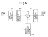
- Figure 6 is a block diagram showing one configuration example for implementing the driving method of Figure 5.
- reference numeral 101 is an image processing section
- 102 is an error diffusion processing section
- 103 is an addition/subtraction determining section
- 104 is an addition/subtraction operation section
- 105 is a subfield (SF) data converting section.
- an input signal Din input into the image processing section 101 is supplied directly to the error diffusion processing section 102, and a value output from the addition/subtraction determining section 103 is added to (or subtracted from) the error-diffused image signal in the addition/subtraction operation section 104.
- the addition/subtraction determining section 103 which receives the output of the error diffusion processing section 102 and determines whether the operation to be performed is an addition or subtraction, supplies a correction value "+2" for the input grayscale level 3 to the addition/subtraction operation section 104, as a result of which a signal with +2 added to the output of the error diffusion processing section 102 is fed to the SF data converting section 105.
- the SF data converting section 105 outputs the grayscale level obtained by adding "+2" to the input grayscale level as an output signal Dout, thus eliminating the brightness step and producing a display retaining grayscale continuity.
- Figures 5 and 6 have been described for the case in which only one brightness step has occurred due to the combination of the light emission subfields, but in actuality, such brightness steps occur at a plurality of locations (for example, at about six locations), and the above addition (or subtraction) operation is performed for each brightness step portion.
- a previously-proposed display apparatus driving method that uses a grayscale continuity compensating light-emission SF pattern table, as earlier described, requires a large capacity memory (table) to store an enormous amount of table covering every possible combination of the subfields.
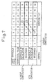
- Figure 7 is a diagram for explaining the problem associated with a previously-proposed display apparatus driving method according to the related art.
- the brightness corresponding to the input grayscale level 3 is set, for example, to "14", in which case the brightness step with respect to the brightness "8" for the input grayscale level 2 is "6".
- the smallest unit of subfield weight is "4".
- the brightness can be controlled only in steps of "4" defined as the smallest unit of subfield weight, if the operation to add "+2" to the grayscale level is performed, for example, for the brightness corresponding to the input grayscale level 3, the brightness step cannot be completely eliminated.
- the display apparatus driving method using the related art computation process has the problem that, as the addition/subtraction operation is performed immediately before determining the light emission subfields, control can only be performed in steps equivalent to the smallest unit of subfield weight, and further, when the total number of light emission pulses is varied by power control, the ratio of the number of light emission pulses set for each subfield is displaced from the theoretical value, resulting in a loss of continuity.
- a display apparatus, and a driving method therefor, embodying the present invention will be described in detail below with reference to the drawings.
- a display apparatus, and a driving method therefor, embodying the present invention are not limited in application to interlaced scan PDPs, but can be applied widely to various other display apparatuses.
- the grayscale continuity compensating process is performed, not by using a table (memory), but by computation, thereby preventing an increase in program amount.
- the ratio of the number of light emission pulses among the subfields is disrupted.
- grayscale continuity is retained by compensating for the resulting brightness step by performing the addition/subtraction operation; to achieve this, computation coefficients are varied according to the display load ratio or the total number of light emission pulses.
- field is used by assuming the case of interlaced scanning in which one image frame is made up of two fields, an odd field and an even field, but in the case of progressive scanning in which one image frame is made up of one field, the term “field” can be used interchangeably with "frame”.
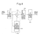
- FIG. 8 is a block diagram showing one configuration example for implementing a display apparatus driving method embodying the present invention.
- reference numeral 201 is an image processing section
- 202 is an error diffusion processing section
- 203 is an addition/subtraction determining section
- 204 is an addition/subtraction operation section
- 205 is a subfield (SF: light emission block) data converting section.
- the addition/subtraction determining section 203 and the addition/subtraction operation section 204 together constitute a grayscale continuity compensating circuit 200.
- the input signal Din is supplied via the image processing section 201 to the addition/subtraction determining section 203 and the addition/subtraction operation section 204, and the output value of the addition/subtraction determining section 203 is added (or subtracted) in the addition/subtraction operation section 204. Then, the output of the addition/subtraction operation section 204 is fed to the error diffusion processing section 202 where error diffusion is applied to the signal resulting from the (addition/subtraction) operation, and the signal with the error diffusion applied thereto is supplied to the SF data converting section 205.
- FIG 9 is a block circuit diagram showing one example of the grayscale continuity compensating circuit that is used in a display apparatus embodying the present invention.
- the grayscale continuity compensating circuit 200 shown here corresponds to the addition/subtraction determining section 203 and addition/subtraction operation section 204 shown in Figure 8.
- the grayscale continuity compensating circuit 200 comprises a comparator 211, an AND gate array 212, a pre-adder 213, and an adder 214.
- the comparator 211 compares the high-order 8 bits (DI[9:2]) of the 10-bit input data DI [9:0] with each of 8-bit correction coefficient appending positions Yn[7:0] (Y0[7:0] to Y15[7:0], see Figure 12), and supplies the results (outputs 20 to Z15) to the AND gate array 212.
- the number of correction coefficient appending positions Yn[7:0] is not limited to 16 (Y0 to Y15), but that the number can be varied in various ways according to the configuration of light emission blocks, etc.
- the AND gate array 212 comprises a plurality of AND gates which AND the respective outputs (Z0 to Z15) of the comparator 211 with respective 4-bit correction coefficients Xn[3:0] (X0[3:0] to X15[3:0]), and the 4-bit outputs of the respective AND gates are added in the pre-adder 213, and the resulting 8-bit output is supplied to the adder 214.
- the adder 214 adds the output of the pre-adder 203 to the input data DI[9:0], and produces a 10-bit output DO[9:0].
- Figure 10 is a flowchart for explaining one example of the operation of the grayscale continuity compensating circuit shown in Figure 9
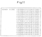
- Figure 11 is a diagram for explaining one example of the operation of the grayscale continuity compensating circuit shown in Figure 9
- Figure 12 is a diagram showing the relationship between output brightness and input grayscale for explaining one example of the operation of the grayscale continuity compensating circuit shown in Figure 9.
- step ST6 the correction coefficient sum B [7:0] (the output of the pre-adder 213 in Figure 9) is added to the input data DI[9:0] to compute the output data DO[9:0] (in the adder 214 shown in Figure 9).
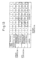
- Figure 13 is a diagram for explaining a first embodiment of a display apparatus driving method embodying the present invention.
- the addition/subtraction determining section 203 and addition/subtraction operation section 204 (grayscale continuity compensating circuit 200) which perform the operation process are placed in front of the error diffusion processing section 202, it becomes possible, for example, to add "+1.5" to the grayscale level for the brightness corresponding to the input grayscale level 3. That is, by performing the operation (addition operation), the brightness for the input grayscale level 3 can be set to "12", providing a grayscale step of "4" with respect to the brightness "8" for the input grayscale level 2; as a result, the brightness step can be completely eliminated.
- the error diffusion by the error diffusion processing section 202 is applied to the output of the addition/subtraction operation section 204 compensated for the above brightness step.
- Figure 14 is a diagram for explaining a second embodiment of a display apparatus driving method embodying the present invention.
- the ideal numbers of light emission pulses for the respective subfields are as shown in Item 1 in Figure 14. That is, when distributing a total of 254 light emission pulses over the subfields SF0 to SF6, the ideal numbers of light emission pulses are 2, 4, 8, 16, 32, 64, and 128 for the subfields SF0, SF1, SF2, SF3, SF4, SF5, and SF6, respectively.
- the total number of light emission pulses is reduced by power control, for example, to 200 as shown in Item 2 in Figure 14; in this case, the numbers of light emission pulses are 2, 3, 6, 13, 25, 50, and 101 for the subfields SF0, SF1, SF2, SF3, SF4, SF5, and SF6, respectively.
- This causes displacements from the above ideal brightness values, disrupting the brightness ratio among the subfields.
- Such brightness ratio displacements would have a significant effect if they occur, among others, in subfields having small weights (for example, SF0, SF1, and SF2); accordingly, in the second embodiment, the numbers of light emission pulses for such subfields are fixed as shown in Item 3 in Figure 14.
- the brightness ratio among the subfields having small weights (SF0 to SF2) is fixed, and power control is performed by reducing the numbers of light emission pulses for the subfields having large weights (SF3 to SF6).
- the brightness steps that occur when exciting such heavily weighted subfields with reduced numbers of light emission pulses are compensated for by performing the earlier described operations in the addition/subtraction determining section 203 and addition/subtraction operation section 204 provided in front of the error diffusion processing section 202.
- Figure 15 is a diagram for explaining a third embodiment of a display apparatus driving method embodying the present invention.
- the ideal numbers of light emission pulses in the respective subfields for the respective total numbers of light emission pulses are as shown in Items 1 to 4 in Figure 15. That is, when the total number of light emission pulses is 127, for example, the ideal numbers of light emission pulses are 1, 2, 4, 8, 16, 32, and 64 (ideal value 1 in Item 1 in Figure 15) for the subfields SF0, SF1, SP2, SF3, SF4, SF5, and SF6, respectively; when the total number of light emission pulses is 254, the ideal numbers are 2, 4, 8, 16, 32, 64, and 128, respectively (ideal value 2 in Item 2 in Figure 15); when the total number of light emission pulses is 381, the ideal numbers are 3, 6, 12, 24, 48, 96, and 192, respectively (ideal value 3 in Item 3 in Figure 15); and when the total number of light emission pulses is 508, the ideal numbers are 4, 8, 16, 32, 64, 128, and 256, respectively (ideal value 4 in Item 4 in Figure 15).
- the subfield (SFO) having the smallest weight is taken as a reference and, based on its brightness, the numbers of light emission pulses in the respective subfields (SF0 to SF6) are determined to achieve the ideal brightness ratio (ideal values 1 to 4).
- the ideal value for the total number of light emission pulses that is larger than and closest to the total number of light emission pulses determined by power control for example, is taken as a reference, based on which the numbers of light emission pulses are fixed and increased or decreased, respectively.
- the ideal numbers of light emission pulses for the respective fields shown in Item 3 in Figure 15 (ideal value 3) are taken as the reference.
- switching among ideal values 1 to 4 may be made, for example, by reference to the ideal value for the total number of light emission pulses that is closest to the total number of light emission pulses determined by power control and, based on this reference, the numbers of light emission pulses may be fixed and increased or decreased, respectively.
- control may be performed, for example, by increasing the numbers of light emission pulses for the subfields having large weights (SF3 to SF6) while holding fixed the brightness ratio among the subfields having small weights (SF0 to SF2).
- the ideal numbers of light emission pulses for the respective fields shown in Item 2 in Figure 15 are taken as the reference.
- Figure 16 is a diagram for explaining the error diffusion process applied to an embodiment of the present invention
- Figure 17 is a circuit diagram showing one example for implementing the error diffusion process shown in Figure 16.
- the error diffusion process used in each of the above-described embodiments can make use of prior known techniques, an example of which is described below.
- the output of the second delay means D2 is supplied through a third delay means D3 to an 13 terminal on the operation means OP2, thereby generating the error data to be distributed to the pixel portion P 3
- the output of the third delay means D3 is supplied through a fourth delay means D4 to an 12 terminal on the operation means OP2, thereby generating the error data to be distributed to the pixel portion P 2
- the third delay means D3 has a delay function (1DT) equivalent to one dot
- the fourth delay means D4 also has a delay function (1DT) equivalent to one dot.
- the low-order bit and some lower order bits of the data input are processed, the signals to be supplied to the inputs I1 to I4 of the operation means OP2 are aligned in phase by using the dot or line delay elements D1 to D4, the error diffusion such as described above is performed by the operation means OP2, and when the error is accumulated until the output data resume bit rises, a value higher by one grayscale level is output. Since the remaining error is fed back to the operation means OP1, there always remains an error in each field, and the number of grayscale levels can thus be increased. It will be appreciated that the error diffusion process applied to an embodiment of the present invention is not limited to the above particular example.
- an embodiment of the present invention provides a display apparatus capable of performing power control while retaining grayscale continuity, and a method for driving the same.
Landscapes
- Engineering & Computer Science (AREA)
- Physics & Mathematics (AREA)
- Computer Hardware Design (AREA)
- General Physics & Mathematics (AREA)
- Theoretical Computer Science (AREA)
- Plasma & Fusion (AREA)
- Power Engineering (AREA)
- Control Of Indicators Other Than Cathode Ray Tubes (AREA)
- Control Of Gas Discharge Display Tubes (AREA)
- Transforming Electric Information Into Light Information (AREA)
Abstract
when adjusting the number of light emission pulses for power control, determining the number of light emission pulses for each of said plurality of light emission blocks while holding unchanged the number of light emission pulses for each light emission block that has a relatively small number of light emission pulses; and
setting a plurality of ideal values for the combination of said light emission blocks by using, as a reference, the brightness of the light emission block having the smallest weight and, of said plurality of ideal values, selecting, as a reference, the ideal value whose total number of light emission pulses is closest to the total number of light emission pulses determined by power control.
Description
- The present invention relates to a display apparatus and a method for driving the same and, more particularly to a display apparatus, such as a plasma display panel (PDP), that has, in each field, a plurality of light emission blocks each comprising a plurality of light emission pulses, and that displays a grayscale by combining these light emission blocks, and a method for driving such a display apparatus.
- With the recent trend toward larger-screen displays, the need for thin display apparatuses has been increasing, and various types of thin display apparatus have been commercially implemented. Examples include matrix panels that display images by directly using digital signals, such as PDPs and other gas discharge display panels, digital micromirror devices (DMDs), EL display devices, fluorescent display tubes, and liquid crystal display devices. Among such thin display devices, gas discharge display panels are considered to be the most promising candidate for large-area, direct-view HDTV (high-definition television) display devices, because of the simple production process which facilitates fabrication of larger-area displays, the self-luminescent property which ensures good display quality, and the high response speed.
- For example, in a PDP, one field is divided into a plurality of light emission blocks (subfields: SFs) each comprising a plurality of light emission pulses, and a grayscale is displayed by combining these light emission blocks. The power consumed by the light emission of the PDP is approximately proportional to the number of light emission pulses (sustain pulses) applied to sustain the light emission, and the power consumption of the PDP can be controlled by controlling the total number of light emission pulses in each field. The number of light emission pulses must be controlled without causing image degradation but, when a specified number of light emission pulses is assigned to each individual subfield, a grayscale discontinuity may occur depending on the total number of light emission pulses. In view of this, in the case of a display apparatus for displaying a grayscale by combining light emission blocks, it is desired to provide a display apparatus that can control the power consumed by light emission while retaining continuity of light emission by performing control so that the brightness varies smoothly over a discontinuous grayscale portion (stepped portion), and to also provide a method for driving such a display apparatus.
- In this specification, the term "field" is used by assuming the case of interlaced scanning in which one image frame is made up of two fields, an odd field and an even field, but in the case of progressive scanning in which one image frame is made up of one field, the term "field" can be used interchangeably with "frame".
- In previously-proposed devices, light emission pulses are set, for example, by calculating a display load ratio for each frame from display data and by performing computation based on the display load ratio for each frame (field) so that the power consumption of the display apparatus will not exceed a predetermined value. Such techniques are disclosed, for example, in
Japanese Unexamined Patent Publication (Kokai) Nos. 06-332397 2000-098970 - More specifically, Japanese Unexamined Patent Publication (Kokai)
No. 06-332397 Japanese Unexamined Patent Publication No. 2000-098970 - The prior art, the related art, and their associated problems will be described in detail later with reference to the accompanying drawings.
- Accordingly, it is desirable to provide a display apparatus that can control power while retaining grayscale continuity, and a method for driving such a display apparatus.
- According to an embodiment of a first aspect of the present invention, there is provided a method for driving a display apparatus that has a predetermined plural number of light emission blocks in each field, and that displays a grayscale by combining the light emission blocks wherein, for any brightness discontinuous portion occurring due to the combination of the light emission blocks, a grayscale level addition/subtraction operation is performed by computation on the discontinuous grayscale in accordance with an input grayscale level.
- According to an embodiment of a second aspect of the present invention, there is provided a method for driving a display apparatus that has a predetermined plural number of light emission blocks in each field, and that displays a grayscale by combining the light emission blocks, wherein for any brightness discontinuous portion occurring due to the combination of the light emission blocks, a grayscale level addition/subtraction operation is performed on the discontinuous grayscale in accordance with an input grayscale level before applying error diffusion.
- According to an embodiment of a third aspect of the present invention, there is provided a method for driving a display apparatus that has in each field a predetermined plural number of light emission blocks each comprising a plurality of light emission pulses, and that displays grayscale by combining the light emission blocks wherein, when adjusting the number of light emission pulses for power control, the number of light emission pulses is determined for each of the plurality of light emission blocks while holding unchanged the number of light emission pulses for each light emission block that has a relatively small number of light emission pulses.
- A plurality of ideal values may be set for the combination of the light emission blocks by using as a reference the brightness of the light emission block having the smallest weight and, from the plurality of ideal values, the ideal value whose total number of light emission pulses is larger than, and closest to, the total number of light emission pulses determined by power control is selected as a reference. Alternatively, a plurality of ideal values may be set for the combination of the light emission blocks by using as a reference the brightness of the light emission block having the smallest weight and, from the plurality of ideal values, the ideal value whose total number of light emission pulses is closest to the total number of light emission pulses determined by power control is selected as a reference.
- For any discontinuous grayscale of brightness occurring as a result of the adjustment of the number of light emission pulses, a grayscale level addition/subtraction operation may be performed by computation in accordance with a display ratio. For any discontinuous grayscale of brightness occurring as a result of the adjustment of the number of light emission pulses, a grayscale level addition/subtraction operation may be performed in accordance with a display ratio before applying error diffusion.
- According to an embodiment of a fourth aspect of the present invention, there is provided a display apparatus that has a predetermined plural number of light emission blocks in each field, and that displays grayscale by combining the light emission blocks, comprising an addition/subtraction determining section which receives an image signal, and determines whether an addition or subtraction operation is to be applied to a brightness discontinuous portion occurring due to the combination of the light emission blocks; and an addition/subtraction operation section which, based on an output of the addition/subtraction determining section, performs for the brightness discontinuous portion a grayscale level addition or subtraction operation by computation on discontinuous grayscale in accordance with an input grayscale level.
- Further, according to an embodiment of a fifth aspect of the present invention, there is provided a display apparatus that has a predetermined plural number of light emission blocks in each field, and that displays grayscale by combining the light emission blocks, comprising an addition/subtraction determining section which receives an image signal, and determines whether an addition or subtraction operation is to be applied to a brightness discontinuous portion occurring due to the combination of the light emission blocks; an error diffusion processing section for applying error diffusion to the image signal; and an addition/subtraction operation section which precedes the error diffusion processing section, and which, based on an output of the addition/subtraction determining section, performs for the brightness discontinuous portion a grayscale level addition or subtraction operation on discontinuous grayscale in accordance with an input grayscale level.
- According to an embodiment of a sixth aspect of the present invention, there is provided a display apparatus comprising a display panel section; a data converter which receives an image signal and supplies image data suitable for the display apparatus to the display panel section, while at the same time, outputting a display load ratio by computing the same from the image signal; a, power supply section which supplies power to the display panel section and, at the same time, outputs information concerning the power being consumed by the display panel section; and a number-of-light-emission-pulses control circuit which receives the display load ratio and the power consumption information and, when adjusting the number of light emission pulses to control the power, determines the number of light emission pulses for each of the plurality of light emission blocks while holding unchanged the number of light emission pulses for each light emission block that has a relatively small number of light emission pulses.
- The number-of-light-emission-pulses control circuit may set a plurality of ideal values for the combination of the light emission blocks by using, as a reference, the brightness of the light emission block having the smallest weight and, from among the plurality of ideal values, may select as a reference the ideal value whose total number of light emission pulses is larger than and closest to the total number of light emission pulses determined by power control. The number-of-light-emission-pulses control circuit may set a plurality of ideal values for the combination of the light emission blocks by using as a reference the brightness of the light emission block having the smallest weight and, from among the plurality of ideal values, may select as a reference the ideal value whose total number of light emission pulses is closest to the total number of light emission pulses determined by power control.
- A display apparatus embodying the present invention may further comprise a grayscale continuity compensating circuit which compensates grayscale continuity by performing a grayscale level addition/subtraction operation by computation in accordance with a display ratio for any discontinuous grayscale of brightness occurring as a result of the adjustment of the number of light emission pulses. A display apparatus embodying the present invention may further comprise an error diffusion processing section which applies error diffusion to the image signal; and a grayscale continuity compensating circuit which precedes the error diffusion processing section, and which compensates for grayscale continuity by performing a grayscale level addition/subtraction operation in accordance with a display ratio for any discontinuous grayscale of brightness occurring as a result of the adjustment of the number of light emission pulses.
- Reference will now be made, by way of example, to the accompanying drawings, in which:
- Figure 1 is a block diagram showing one example of a display apparatus to which an embodiment of the present invention is applied;
- Figure 2 is a diagram for explaining one example of a driving method for the display apparatus shown in Figure 1;
- Figure 3 is a diagram showing how the total number of light emission pulses is divided in accordance with a weight ratio among subfields;
- Figures 4A and 4B are diagrams for explaining the problem associated with a previously-proposed display apparatus driving method;
- Figure 5 is a diagram for explaining one example of a previously-proposed display apparatus driving method according to the related art;
- Figure 6 is a block diagram showing one configuration example for implementing the driving method of Figure 5;
- Figure 7 is a diagram for explaining the problem associated with a previously-proposed display apparatus driving method according to the related art;
- Figure 8 is a block diagram showing one configuration example for implementing a display apparatus driving method embodying the present invention;
- Figure 9 is a block circuit diagram showing one example of a grayscale continuity compensating circuit that is used in a display apparatus embodying the present invention;
- Figure 10 is a flowchart for explaining one example of the operation of the grayscale continuity compensating circuit shown in Figure 9;
- Figure 11 is a diagram for explaining one example of the operation of the grayscale continuity compensating circuit shown in Figure 9;
- Figure 12 is a diagram showing the relationship between output brightness and input grayscale for explaining one example of the operation of the grayscale continuity compensating circuit shown in Figure 9;
- Figure 13 is a diagram for explaining a first embodiment of a display apparatus driving method embodying the present invention;
- Figure 14 is a diagram for explaining a second embodiment of a display apparatus driving method embodying the present invention;
- Figure 15 is a diagram for explaining a third embodiment of a display apparatus driving method embodying the present invention;
- Figure 16 is a diagram for explaining an error diffusion process applied to an embodiment of the present invention; and
- Figure 17 is a circuit diagram showing one example for implementing the error diffusion process shown in Figure 16.
- Before proceeding to a detailed description of the preferred embodiments of a display apparatus, and a driving method therefore embodying the present invention, a display apparatus and its driving method according to the prior art and the related art and their problems will be described, with reference to the drawings.
- Figure 1 is a block diagram showing one example of a display apparatus to which an embodiment of the present invention is applied; here, one example of a plasma display apparatus (plasma display panel: PDP) is illustrated. In Figure 1,
reference numeral 1 is a data converter, 2 is a frame memory, 3 is a power control circuit, 4 is a driver control circuit, 5 is a power supply, 6 is an address driver, 7 is a Y driver, 8 is an X driver, and 9 is a display panel. - As shown in Figure 1, the
data converter 1 receives an image signal and a vertical synchronization signal Vsync from the outside, and converts them into PDP display data (data for displaying an image using a plurality of light emission blocks (subfields SFs)). Theframe memory 2 holds the PDP display data converted by thedata converter 1 for use in the next field. Thedata converter 1 then reads the data previously held in theframe memory 2 and supplies it as address data to theaddress driver 6, while at the same time, providing its display load ratio to thedriver control circuit 4. Here, the display load ratio is found by counting the number of cells to be excited (dots to be illuminated) in each light emission block. - The
driver control circuit 4 receives from the power control circuit 3 a control signal for controlling the number of light emission pulses (sustain pulses) for each light emission block (SF) and an internally generated vertical synchronization signal Vsync2, and supplies drive control-data to theY driver 7. The data signal of the display load ratio, output from thedata converter 1, is supplied to thepower control circuit 3 via thedriver control circuit 4. - The
display panel 9 includes address electrodes A1 to Am, Y electrodes Y1 to Yn, and X electrodes X, which are driven by theaddress driver 6, theY driver 7, and theX driver 8, respectively. Thepower supply 5, while supplying power to theaddress driver 6,Y driver 7, andX driver 8, detects voltages and currents from theaddress driver 6,Y driver 7, andX driver 8 and supplies the detected values to thepower control circuit 3. That is, the address voltage and current from theaddress driver 6 and the sustain voltage and current from theY driver 7 andX driver 8 are detected, and the detected values are supplied from thepower supply 5 to thepower control circuit 3 for processing therein. Theaddress driver 6, theY driver 7, theX driver 8, and thedisplay panel 9 together constitute the display panel section. - Figure 2 is a diagram for explaining one example of a driving method for the display apparatus shown in Figure 1.
- The driving method shown in Figure 2 displays one image frame by interlacing two fields, an odd field and an even field, and the odd field and the even field are each made up of a plurality of light emission blocks (subfields, for example, seven subfields SF0 to SF6). Each of the light emission blocks SF0 to SF6 has an address period, during which address discharge is performed to excite cells in accordance with the address data, and a light emission period (sustain discharge period), during which light emission pulses (sustain pulses) are applied to the selected cells (illuminated cells) to sustain the light emission state.
- Figure 3 is a diagram showing how the total number of light emission pulses is divided in accordance with a weight ratio among the subfields.
- As shown in Figure 3, the total number of light emission pulses, which is determined by the display load ratio, is divided in accordance with the weight ratio among the subfields. More specifically, when the total number of light emission pulses is 508, for example, the number of light emission pulses assigned in accordance with the weight ratio among the subfields SF0 to SF6 is 4 for SF0, 8 for SF1, 16 for SF2, 32 for SF3, 64 for SF4, 128 for SF5, and 256 for SF6.
- Figures 4A and 4B are diagrams for explaining the problem associated with a previously-proposed display apparatus driving method: Figure 4A shows the relationship between brightness and the number of light emission pulses, and Figure 4B shows the relationship between output brightness and input grayscale.
- As shown in Figure 4A, the relationship between the brightness and the number of light emission pulses is not linear because of the brightness saturation of phosphors, and there occurs (as shown in Figure 4B) a brightness step because the brightness of each subfield (SF) falls short of expected brightness, or a brightness step because discharge spreads into non-illuminated pixels due to overlay or other processing.
- That is, grayscale continuity cannot be secured by just dividing the total number of light emission pulses in accordance with the subfield weight ratio. One possible solution to this problem is to increase the number of light emission pulses in each subfield by considering the brightness saturation or to decrease the number of light emission pulses by considering the increase of brightness due to discharge spreading.
- However, by just adjusting the number of light emission pulses in each subfield as described above, grayscale continuity cannot be secured in a reliable manner. This is because there occurs a brightness step depending on the combination of the light emission subfields, even though the brightness of each subfield itself is exactly as defined by its weight ratio.
- To address this brightness step, it has been previously-proposed to hold a grayscale continuity compensating light-emission SF (subfield) pattern in the form of a table (in a memory) and to correct the step by choosing an appropriate combination of the light emission subfields. According to the related art, a method that corrects the brightness step by computation without using such a light-emission SF pattern table has been previously-proposed.
- Figure 5 is a diagram for explaining one example of a previously-proposed display apparatus driving method according to the related art, and Figure 6 is a block diagram showing one configuration example for implementing the driving method of Figure 5. In Figure 6,
reference numeral 101 is an image processing section, 102 is an error diffusion processing section, 103 is an addition/subtraction determining section, 104 is an addition/subtraction operation section, and 105 is a subfield (SF) data converting section. - In the driving method shown in Figure 5, and in, for example, the case where when the input grayscale level is 3, the theoretical value of brightness is also 3, but the actual brightness corresponding to the
grayscale level 3 obtained by calculation is 1; in such a case, operations are performed to make the grayscale level that is 5 by calculation, and at which the actual brightness is the same as the theoretical value of 3, correspond to theinput grayscale level 3. - As shown in Figure 6, an input signal Din input into the
image processing section 101 is supplied directly to the errordiffusion processing section 102, and a value output from the addition/subtraction determining section 103 is added to (or subtracted from) the error-diffused image signal in the addition/subtraction operation section 104. More specifically, in the case shown in Figure 5, since there is a brightness step of -2 with respect to the theoretical value of brightness for the input grayscale level 3 (theinput grayscale levels 3 and larger), the addition/subtraction determining section 103, which receives the output of the errordiffusion processing section 102 and determines whether the operation to be performed is an addition or subtraction, supplies a correction value "+2" for theinput grayscale level 3 to the addition/subtraction operation section 104, as a result of which a signal with +2 added to the output of the errordiffusion processing section 102 is fed to the SFdata converting section 105. - That is, for the
input grayscale levels 3 and larger, the SFdata converting section 105 outputs the grayscale level obtained by adding "+2" to the input grayscale level as an output signal Dout, thus eliminating the brightness step and producing a display retaining grayscale continuity. Figures 5 and 6 have been described for the case in which only one brightness step has occurred due to the combination of the light emission subfields, but in actuality, such brightness steps occur at a plurality of locations (for example, at about six locations), and the above addition (or subtraction) operation is performed for each brightness step portion. - On the other hand, a previously-proposed display apparatus driving method that uses a grayscale continuity compensating light-emission SF pattern table, as earlier described, requires a large capacity memory (table) to store an enormous amount of table covering every possible combination of the subfields.
- Figure 7 is a diagram for explaining the problem associated with a previously-proposed display apparatus driving method according to the related art.
- As shown in Figure 7, according to the related art described with reference to Figures 5 and 6, when the (addition) operation is performed, the brightness corresponding to the
input grayscale level 3 is set, for example, to "14", in which case the brightness step with respect to the brightness "8" for theinput grayscale level 2 is "6". Here, the smallest unit of subfield weight is "4". - In this case, since, in the related art, the brightness can be controlled only in steps of "4" defined as the smallest unit of subfield weight, if the operation to add "+2" to the grayscale level is performed, for example, for the brightness corresponding to the
input grayscale level 3, the brightness step cannot be completely eliminated. - That is, the display apparatus driving method using the related art computation process has the problem that, as the addition/subtraction operation is performed immediately before determining the light emission subfields, control can only be performed in steps equivalent to the smallest unit of subfield weight, and further, when the total number of light emission pulses is varied by power control, the ratio of the number of light emission pulses set for each subfield is displaced from the theoretical value, resulting in a loss of continuity.
- A display apparatus, and a driving method therefor, embodying the present invention will be described in detail below with reference to the drawings. Here, it will be recognized that a display apparatus, and a driving method therefor, embodying the present invention are not limited in application to interlaced scan PDPs, but can be applied widely to various other display apparatuses.
- In an embodiment of the present invention, the grayscale continuity compensating process is performed, not by using a table (memory), but by computation, thereby preventing an increase in program amount. In an embodiment of the present invention, it is possible to perform the addition/subtraction computation process, not only on integers, but also on numbers containing decimal fractions, by placing the computation process in front of the error diffusion process. Typically, when the total number of light emission pulses is reduced by power control, the ratio of the number of light emission pulses among the subfields is disrupted. However, in an embodiment of the present invention, grayscale continuity is retained by compensating for the resulting brightness step by performing the addition/subtraction operation; to achieve this, computation coefficients are varied according to the display load ratio or the total number of light emission pulses.
- In this specification, the term "field" is used by assuming the case of interlaced scanning in which one image frame is made up of two fields, an odd field and an even field, but in the case of progressive scanning in which one image frame is made up of one field, the term "field" can be used interchangeably with "frame".
- Figure 8 is a block diagram showing one configuration example for implementing a display apparatus driving method embodying the present invention. In Figure 8,
reference numeral 201 is an image processing section, 202 is an error diffusion processing section, 203 is an addition/subtraction determining section, 204 is an addition/subtraction operation section, and 205 is a subfield (SF: light emission block) data converting section. Here, the addition/subtraction determining section 203 and the addition/subtraction operation section 204 together constitute a grayscalecontinuity compensating circuit 200. - As is apparent from a comparison between Figure 8 and the earlier described Figure 6, in the configuration shown in Figure 8 the addition/
subtraction determining section 203 and the addition/subtraction operation section 204 are placed in front of the errordiffusion processing section 202. - As shown in Figure 8, the input signal Din is supplied via the
image processing section 201 to the addition/subtraction determining section 203 and the addition/subtraction operation section 204, and the output value of the addition/subtraction determining section 203 is added (or subtracted) in the addition/subtraction operation section 204. Then, the output of the addition/subtraction operation section 204 is fed to the errordiffusion processing section 202 where error diffusion is applied to the signal resulting from the (addition/subtraction) operation, and the signal with the error diffusion applied thereto is supplied to the SFdata converting section 205. - Figure 9 is a block circuit diagram showing one example of the grayscale continuity compensating circuit that is used in a display apparatus embodying the present invention. The grayscale
continuity compensating circuit 200 shown here corresponds to the addition/subtraction determining section 203 and addition/subtraction operation section 204 shown in Figure 8. - As shown in Figure 9, the grayscale
continuity compensating circuit 200 comprises acomparator 211, an ANDgate array 212, a pre-adder 213, and anadder 214. Thecomparator 211 compares the high-order 8 bits (DI[9:2]) of the 10-bit input data DI [9:0] with each of 8-bit correction coefficient appending positions Yn[7:0] (Y0[7:0] to Y15[7:0], see Figure 12), and supplies the results (outputs 20 to Z15) to the ANDgate array 212. Here, it will be appreciated that the number of correction coefficient appending positions Yn[7:0] is not limited to 16 (Y0 to Y15), but that the number can be varied in various ways according to the configuration of light emission blocks, etc. - The AND
gate array 212 comprises a plurality of AND gates which AND the respective outputs (Z0 to Z15) of thecomparator 211 with respective 4-bit correction coefficients Xn[3:0] (X0[3:0] to X15[3:0]), and the 4-bit outputs of the respective AND gates are added in the pre-adder 213, and the resulting 8-bit output is supplied to theadder 214. Theadder 214 adds the output of the pre-adder 203 to the input data DI[9:0], and produces a 10-bit output DO[9:0]. - Figure 10 is a flowchart for explaining one example of the operation of the grayscale continuity compensating circuit shown in Figure 9, Figure 11 is a diagram for explaining one example of the operation of the grayscale continuity compensating circuit shown in Figure 9, and Figure 12 is a diagram showing the relationship between output brightness and input grayscale for explaining one example of the operation of the grayscale continuity compensating circuit shown in Figure 9.
- First, when the input data Din is input into the grayscale continuity compensating circuit 200 (addition/subtraction determining section 203) via the
image processing section 201, in step ST1 the high-order 8 bit part (DI[9:2]) of the input data Din (10-bit input data DI[9:0]) is set as A (DI[9:2] = A), the correction coefficient appending position as Yn[7:0], and the correction coefficient as Xn[3:0]. Further, the output data (10-bit output data) of the grayscale continuity compensating circuit 200 (addition/subtraction operation section 204) is set as DO[9:0]. Next, the process proceeds to step ST2 where n is set to 0, and then the process proceeds to step ST3 where A is compared with Yn (in thecomparator 211 shown in Figure 9). - If it is determined in step ST3 that the relation A≥Yn holds, the process proceeds to step ST4 where the correction coefficient is added to a correction coefficient sum B[7:0] (B[7:0] = B[7:0] + Xn[3:0]). The process then proceeds to step ST5 to increment n by 1 (n = n + 1), and returns to step ST3 to repeat the same process until it is determined that A≥Yn no longer holds (A<Yn holds). That is, corrections are applied for all the correction coefficient appending positions Yn (for example, 16 correction coefficient appending positions Y0 to Y15 are corrected using the correction coefficients Xn (X0 to X15), see Figure 12).
- When it is determined in step ST3 that A≥Yn no longer holds, the process proceeds to step ST6 where the correction coefficient sum B [7:0] (the output of the pre-adder 213 in Figure 9) is added to the input data DI[9:0] to compute the output data DO[9:0] (in the
adder 214 shown in Figure 9). - In this way, the operation such as shown in Figure 11 (for compensating for every brightness step in the input data DI[9:0]) is performed, and the output data DO[9:0] is produced. The output data of the grayscale continuity compensating circuit 200 (addition/subtraction operation section 204) is supplied to the error
diffusion processing section 202 at the next stage for error diffusion. - Figure 13 is a diagram for explaining a first embodiment of a display apparatus driving method embodying the present invention.
- As is apparent from a comparison between Figure 13 and the previously described Figure 7, and as, in the first embodiment, the addition/
subtraction determining section 203 and addition/subtraction operation section 204 (grayscale continuity compensating circuit 200) which perform the operation process are placed in front of the errordiffusion processing section 202, it becomes possible, for example, to add "+1.5" to the grayscale level for the brightness corresponding to theinput grayscale level 3. That is, by performing the operation (addition operation), the brightness for theinput grayscale level 3 can be set to "12", providing a grayscale step of "4" with respect to the brightness "8" for theinput grayscale level 2; as a result, the brightness step can be completely eliminated. Here, the error diffusion by the errordiffusion processing section 202 is applied to the output of the addition/subtraction operation section 204 compensated for the above brightness step. - Figure 14 is a diagram for explaining a second embodiment of a display apparatus driving method embodying the present invention.
- First, it is assumed that when the number of light emission pulses (sustain pulses: SUSs) is distributed over the respective subfields, the ideal numbers of light emission pulses for the respective subfields are as shown in
Item 1 in Figure 14. That is, when distributing a total of 254 light emission pulses over the subfields SF0 to SF6, the ideal numbers of light emission pulses are 2, 4, 8, 16, 32, 64, and 128 for the subfields SF0, SF1, SF2, SF3, SF4, SF5, and SF6, respectively. - Suppose here that the total number of light emission pulses is reduced by power control, for example, to 200 as shown in
Item 2 in Figure 14; in this case, the numbers of light emission pulses are 2, 3, 6, 13, 25, 50, and 101 for the subfields SF0, SF1, SF2, SF3, SF4, SF5, and SF6, respectively. This causes displacements from the above ideal brightness values, disrupting the brightness ratio among the subfields. Such brightness ratio displacements would have a significant effect if they occur, among others, in subfields having small weights (for example, SF0, SF1, and SF2); accordingly, in the second embodiment, the numbers of light emission pulses for such subfields are fixed as shown inItem 3 in Figure 14. That is, in the second embodiment, the brightness ratio among the subfields having small weights (SF0 to SF2) is fixed, and power control is performed by reducing the numbers of light emission pulses for the subfields having large weights (SF3 to SF6). The brightness steps that occur when exciting such heavily weighted subfields with reduced numbers of light emission pulses are compensated for by performing the earlier described operations in the addition/subtraction determining section 203 and addition/subtraction operation section 204 provided in front of the errordiffusion processing section 202. - Figure 15 is a diagram for explaining a third embodiment of a display apparatus driving method embodying the present invention.
- First, it is assumed that the ideal numbers of light emission pulses in the respective subfields for the respective total numbers of light emission pulses are as shown in
Items 1 to 4 in Figure 15. That is, when the total number of light emission pulses is 127, for example, the ideal numbers of light emission pulses are 1, 2, 4, 8, 16, 32, and 64 (ideal value 1 inItem 1 in Figure 15) for the subfields SF0, SF1, SP2, SF3, SF4, SF5, and SF6, respectively; when the total number of light emission pulses is 254, the ideal numbers are 2, 4, 8, 16, 32, 64, and 128, respectively (ideal value 2 inItem 2 in Figure 15); when the total number of light emission pulses is 381, the ideal numbers are 3, 6, 12, 24, 48, 96, and 192, respectively (ideal value 3 inItem 3 in Figure 15); and when the total number of light emission pulses is 508, the ideal numbers are 4, 8, 16, 32, 64, 128, and 256, respectively (ideal value 4 inItem 4 in Figure 15). - In this way, in the third embodiment, the subfield (SFO) having the smallest weight is taken as a reference and, based on its brightness, the numbers of light emission pulses in the respective subfields (SF0 to SF6) are determined to achieve the ideal brightness ratio (
ideal values 1 to 4). Here, as for switching amongideal values 1 to 4, the ideal value for the total number of light emission pulses that is larger than and closest to the total number of light emission pulses determined by power control, for example, is taken as a reference, based on which the numbers of light emission pulses are fixed and increased or decreased, respectively. In a specific example, if the total number of light emission pulses determined by power control is 350, then the ideal numbers of light emission pulses for the respective fields shown inItem 3 in Figure 15 (ideal value 3) are taken as the reference. - Alternatively, switching among
ideal values 1 to 4 may be made, for example, by reference to the ideal value for the total number of light emission pulses that is closest to the total number of light emission pulses determined by power control and, based on this reference, the numbers of light emission pulses may be fixed and increased or decreased, respectively. Here, for example, when the total number of light emission pulses determined by power control is larger than the ideal value for the total number of light emission pulses taken as the reference, control may be performed, for example, by increasing the numbers of light emission pulses for the subfields having large weights (SF3 to SF6) while holding fixed the brightness ratio among the subfields having small weights (SF0 to SF2). In this example, if the total number of light emission pulses determined by power control is 300, then the ideal numbers of light emission pulses for the respective fields shown inItem 2 in Figure 15 (ideal value 2) are taken as the reference. - Figure 16 is a diagram for explaining the error diffusion process applied to an embodiment of the present invention, and Figure 17 is a circuit diagram showing one example for implementing the error diffusion process shown in Figure 16.
- The error diffusion process used in each of the above-described embodiments, that is, the error diffusion process performed in the error
diffusion processing section 202 in Figure 8, can make use of prior known techniques, an example of which is described below. - First, as shown in Figure 16, when causing all the pixels in an image display to display respectively designated halftone image data, attention is paid to a particular pixel portion P0, and also to the line n to which this particular pixel portion P0 belongs and the line n+1 to be scanned next. Then, error data is distributed in prescribed proportions over a total of four pixel portions, i.e., the pixel portion P1 adjacent to the right of the particular pixel portion P0 in the scanning direction and the pixel portions P2, P3, and P4 located on the line n+1 at positions lower left, below, and lower right with respect to P0. Here, a prior known configuration can be employed for the error diffusion processing operation circuit used to accomplish the above error diffusion process; one example of the circuit is shown in Figure 17.
- That is, as shown in Figure 17, when halftone image data DIN (13 to 0) is input to an operation means OP1, and the output of the operation means OP1 is passed through a first delay means D1 and delivered as an output DOUT (7 to 0), for example, the output is also supplied through a second delay means D2 to an I4 terminal on an operation means OP2, thereby generating the error data to be distributed to the pixel portion P4. The output the operation means OP1 passed through the first delay means D1 is also supplied directly to an I1 terminal on the operation means OP2, thereby generating the error data to be distributed to the pixel portion P1. Here, the first delay means D1 has a delay function (1DT) equivalent to one dot, while the second delay means D2 has a delay function (1H-2DT) equivalent to one line or two dots.
- Further, the output of the second delay means D2 is supplied through a third delay means D3 to an 13 terminal on the operation means OP2, thereby generating the error data to be distributed to the pixel portion P3, and the output of the third delay means D3 is supplied through a fourth delay means D4 to an 12 terminal on the operation means OP2, thereby generating the error data to be distributed to the pixel portion P2. Here, the third delay means D3 has a delay function (1DT) equivalent to one dot, and the fourth delay means D4 also has a delay function (1DT) equivalent to one dot.
- The above error diffusion method is well known in the art; that is, in Figure 16, the error at a particular dot P0 is diffused over its neighboring dots P1, P2, P3, and P4, distributing its value as P1 = (7/16)×P0, P2 = (1/16)×P0, P3 = (5/16)×P0, and P4 = (3/16)×P0. In this way, error is diffused by processing the dots from left to right in sequence from top to bottom, to achieve multiple grayscale levels.
- Further, in the error diffusion processing operation circuit shown in Figure 17, the low-order bit and some lower order bits of the data input are processed, the signals to be supplied to the inputs I1 to I4 of the operation means OP2 are aligned in phase by using the dot or line delay elements D1 to D4, the error diffusion such as described above is performed by the operation means OP2, and when the error is accumulated until the output data resume bit rises, a value higher by one grayscale level is output. Since the remaining error is fed back to the operation means OP1, there always remains an error in each field, and the number of grayscale levels can thus be increased. It will be appreciated that the error diffusion process applied to an embodiment of the present invention is not limited to the above particular example.
- As described in detail above, an embodiment of the present invention provides a display apparatus capable of performing power control while retaining grayscale continuity, and a method for driving the same.
- Many different embodiments of the present invention may be constructed without departing from the spirit and scope of the present invention, and it should be understood that the present invention is not limited to the specific embodiments described in this specification.
Claims (13)
- A method for driving a display apparatus that has in each field a predetermined plural number of light emission blocks, each comprising a plurality of light emission pulses, and that displays grayscale by combining said light emission blocks, comprising:when adjusting the number of light emission pulses for power control, determining the number of light emission pulses for each of said plurality of light emission blocks while holding unchanged the number of light emission pulses for each light emission block that has a relatively small number of light emission pulses; andsetting a plurality of ideal values for the combination of said light emission blocks by using, as a reference, the brightness of the light emission block having the smallest weight and, of said plurality of ideal values, selecting, as a reference, the ideal value whose total number of light emission pulses is closest to the total number of light emission pulses determined by power control.
- The method for driving a display apparatus as claimed in claim 1, wherein the ideal value whose total number of light emission pulses is larger than the total number of light emission pulses determined by power control is selected as a reference.
- The method for driving a display apparatus as claimed in claim 1 or 2, wherein, for any discontinuous grayscale of brightness occurring as a result of said adjustment of the number of light emission pulses, a grayscale level addition/subtraction operation is performed by computation in accordance with a display ratio.
- The method for driving a display apparatus as claimed in claim 3, wherein the grayscale level addition/subtraction operation is performed before applying error diffusion.
- A method for driving a display apparatus that has a predetermined plural number of light emission blocks in each field, and that displays grayscale by combining said light emission blocks, wherein:for any brightness discontinuous portion occurring due to the combination of said light emission blocks, a grayscale level addition/subtraction operation is performed by computation on a discontinuous grayscale in accordance with an input grayscale level.
- A method for driving a display apparatus that has a predetermined plural number of light emission blocks in each field, and that displays grayscale by combining said light emission blocks, wherein:for any brightness discontinuous portion occurring due to the combination of said light emission blocks, a grayscale level addition/subtraction operation is performed on a discontinuous grayscale in accordance with an input grayscale level before applying error diffusion.
- A display apparatus that has a predetermined plural number of light emission blocks in each field, and that displays grayscale by combining said light emission blocks, comprising:an addition/subtraction determining section which receives an image signal, and determines whether an addition or subtraction operation is to be applied to a brightness discontinuous portion occurring due to the combination of said light emission blocks; andan addition/subtraction operation section which, based on an output of said addition/subtraction determining section, performs for said brightness discontinuous portion a grayscale level addition or subtraction operation, by computation, on a discontinuous grayscale in accordance with an input grayscale level.
- A display apparatus that has a predetermined plural number of light emission blocks in each field, and that displays grayscale by combining said light emission blocks, comprising:an addition/subtraction determining section which receives an image signal, and determines whether an addition or subtraction operation is to be applied to a brightness discontinuous portion occurring due to the combination of said light emission blocks;an error diffusion processing section for applying error diffusion to said image signal; andan addition/subtraction operation section which precedes said error diffusion processing section, and which, based on an output of said addition/subtraction determining section, performs for said brightness discontinuous portion a grayscale level addition or subtraction operation on a discontinuous grayscale in accordance with an input grayscale level.
- A display apparatus comprising:a display panel section;a data converter which receives an image signal and supplies image data suitable for said display apparatus to said display panel section, while at the same time, outputting a display load ratio by computing the same from said image signal;a power supply section which supplies power to said display panel section and, at the same time, outputs information concerning the power being consumed by said display panel section; anda number-of-light-emission-pulses control circuit which receives said display load ratio and said power consumption information and, when adjusting the number of light emission pulses to control the power, determines the number of light emission pulses for each of said plurality of light emission blocks while holding unchanged the number of light emission pulses for each light emission block that has a relatively small number of light emission pulses.
- The display apparatus as claimed in claim 9, wherein said number-of-light-emission-pulses control circuit sets a plurality of ideal values for the combination of said light emission blocks by using, as a reference, the brightness of the light emission block having the smallest weight and, from among said plurality of ideal values, selects as a reference the ideal value whose total number of light emission pulses is larger than, and closest to, the total number of light emission pulses determined by power control.
- The display apparatus as claimed in claim 9, wherein said number-of-light-emission-pulses control circuit sets a plurality of ideal values for the combination of said light emission blocks by using, as a reference, the brightness of the light emission block having the smallest weight and, from among said plurality of ideal values, selects as a reference the ideal value whose total number of light emission pulses is closest to the total number of light emission pulses determined by power control.
- The display apparatus as claimed in claim 9, 10, or 11, further comprising a grayscale continuity compensating circuit which compensates for grayscale continuity by performing a grayscale level addition/subtraction operation by computation in accordance with a display ratio for any discontinuous grayscale of brightness occurring as a result of said adjustment of the number of light emission pulses.
- The display apparatus as claimed in claim 9, 10 or 11, further comprising:an error diffusion processing section which applies error diffusion to said image signal; anda grayscale continuity compensating circuit which precedes said error diffusion processing section, and which compensates for grayscale continuity by performing a grayscale level addition/subtraction operation in accordance with a display ratio for any discontinuous grayscale of brightness occurring as a result of said adjustment of the number of light emission pulses.
Applications Claiming Priority (2)
| Application Number | Priority Date | Filing Date | Title |
|---|---|---|---|
| JP2002072861A JP5049445B2 (en) | 2002-03-15 | 2002-03-15 | Display device and driving method thereof |
| EP02257440A EP1345198A3 (en) | 2002-03-15 | 2002-10-25 | Plasma display apparatus and subfield driving method therefor |
Related Parent Applications (1)
| Application Number | Title | Priority Date | Filing Date |
|---|---|---|---|
| EP02257440A Division EP1345198A3 (en) | 2002-03-15 | 2002-10-25 | Plasma display apparatus and subfield driving method therefor |
Publications (2)
| Publication Number | Publication Date |
|---|---|
| EP1746564A2 true EP1746564A2 (en) | 2007-01-24 |
| EP1746564A3 EP1746564A3 (en) | 2007-06-06 |
Family
ID=27764574
Family Applications (3)
| Application Number | Title | Priority Date | Filing Date |
|---|---|---|---|
| EP02257440A Withdrawn EP1345198A3 (en) | 2002-03-15 | 2002-10-25 | Plasma display apparatus and subfield driving method therefor |
| EP06122084A Withdrawn EP1746564A3 (en) | 2002-03-15 | 2002-10-25 | Method of driving a plasma display apparatus |
| EP10160502A Withdrawn EP2219171A1 (en) | 2002-03-15 | 2002-10-25 | Plasma display apparatus and subfield driving method therefor |
Family Applications Before (1)
| Application Number | Title | Priority Date | Filing Date |
|---|---|---|---|
| EP02257440A Withdrawn EP1345198A3 (en) | 2002-03-15 | 2002-10-25 | Plasma display apparatus and subfield driving method therefor |
Family Applications After (1)
| Application Number | Title | Priority Date | Filing Date |
|---|---|---|---|
| EP10160502A Withdrawn EP2219171A1 (en) | 2002-03-15 | 2002-10-25 | Plasma display apparatus and subfield driving method therefor |
Country Status (5)
| Country | Link |
|---|---|
| US (1) | US7075560B2 (en) |
| EP (3) | EP1345198A3 (en) |
| JP (1) | JP5049445B2 (en) |
| KR (3) | KR100879421B1 (en) |
| TW (1) | TW559761B (en) |
Families Citing this family (17)
| Publication number | Priority date | Publication date | Assignee | Title |
|---|---|---|---|---|
| EP1353314A1 (en) * | 2002-04-11 | 2003-10-15 | Deutsche Thomson-Brandt Gmbh | Method and apparatus for processing video pictures to improve the greyscale resolution of a display device |
| EP1391865A1 (en) * | 2002-08-23 | 2004-02-25 | Deutsche Thomson-Brandt Gmbh | Plasma display panel (PDP) - Reduction of dithering noise while displaying less video levels than required |
| KR100490542B1 (en) | 2002-11-26 | 2005-05-17 | 삼성에스디아이 주식회사 | Panel driving method and apparatus with address-sustain mixed interval |
| US8289233B1 (en) | 2003-02-04 | 2012-10-16 | Imaging Systems Technology | Error diffusion |
| US8305301B1 (en) | 2003-02-04 | 2012-11-06 | Imaging Systems Technology | Gamma correction |
| KR100495301B1 (en) * | 2003-02-21 | 2005-06-14 | 삼성에스디아이 주식회사 | Image data linearity amending method and apparatus for plasma display panel and a plasma display panel device having that apparatus |
| KR100603310B1 (en) * | 2003-11-22 | 2006-07-20 | 삼성에스디아이 주식회사 | Discharge display panel driving method for increasing linearity of gradation |
| KR20050049668A (en) * | 2003-11-22 | 2005-05-27 | 삼성에스디아이 주식회사 | Driving method of plasma display panel |
| KR100603312B1 (en) | 2003-11-24 | 2006-07-20 | 삼성에스디아이 주식회사 | Driving method of plasma display panel |
| WO2006008798A1 (en) * | 2004-07-16 | 2006-01-26 | Hitachi Plasma Patent Licensing Co., Ltd. | Display driving method |
| JP4563787B2 (en) * | 2004-12-10 | 2010-10-13 | 日立プラズマディスプレイ株式会社 | Plasma display device and control method thereof |
| TWI340375B (en) * | 2006-04-19 | 2011-04-11 | Quanta Comp Inc | Gamma adjusting apparatus and method of the same |
| KR100793104B1 (en) | 2006-07-06 | 2008-01-10 | 엘지전자 주식회사 | Plasma Display Device and Image Processing Method |
| US20100033509A1 (en) * | 2007-03-01 | 2010-02-11 | Panasonic Corporation | Image display device |
| US8248328B1 (en) | 2007-05-10 | 2012-08-21 | Imaging Systems Technology | Plasma-shell PDP with artifact reduction |
| JP2009003461A (en) * | 2008-07-22 | 2009-01-08 | Hitachi Plasma Display Ltd | Display device and driving method therefor |
| CN108550347B (en) * | 2018-05-31 | 2020-11-10 | 京东方科技集团股份有限公司 | Light emission control signal generation device and display device |
Citations (2)
| Publication number | Priority date | Publication date | Assignee | Title |
|---|---|---|---|---|
| JPH06332397A (en) | 1993-05-25 | 1994-12-02 | Fujitsu Ltd | Flat panel display device |
| JP2000098970A (en) | 1993-05-25 | 2000-04-07 | Fujitsu Ltd | Plasma display device |
Family Cites Families (28)
| Publication number | Priority date | Publication date | Assignee | Title |
|---|---|---|---|---|
| JP2856241B2 (en) | 1993-11-17 | 1999-02-10 | 富士通株式会社 | Gradation control method for plasma display device |
| US5943032A (en) * | 1993-11-17 | 1999-08-24 | Fujitsu Limited | Method and apparatus for controlling the gray scale of plasma display device |
| JP3307486B2 (en) * | 1993-11-19 | 2002-07-24 | 富士通株式会社 | Flat panel display and control method thereof |
| JP2820036B2 (en) * | 1994-06-24 | 1998-11-05 | 株式会社富士通ゼネラル | Display device gradation correction circuit |
| DE69529716T2 (en) | 1994-10-06 | 2003-07-17 | Fujitsu General Ltd., Kawasaki | Gray scale processing using an error diffusion technique |
| JP2720801B2 (en) | 1994-10-27 | 1998-03-04 | 日本電気株式会社 | Plasma display panel driving method and plasma display panel driving device |
| JP3139312B2 (en) * | 1994-11-25 | 2001-02-26 | 株式会社富士通ゼネラル | Display driving method and apparatus |
| US6025818A (en) | 1994-12-27 | 2000-02-15 | Pioneer Electronic Corporation | Method for correcting pixel data in a self-luminous display panel driving system |
| JP3891499B2 (en) * | 1995-04-14 | 2007-03-14 | パイオニア株式会社 | Brightness adjustment device for plasma display panel |
| JP3354741B2 (en) * | 1995-04-17 | 2002-12-09 | 富士通株式会社 | Halftone display method and halftone display device |
| US6100859A (en) * | 1995-09-01 | 2000-08-08 | Fujitsu Limited | Panel display adjusting number of sustaining discharge pulses according to the quantity of display data |
| US5818419A (en) * | 1995-10-31 | 1998-10-06 | Fujitsu Limited | Display device and method for driving the same |
| JPH1039829A (en) * | 1996-07-18 | 1998-02-13 | Fujitsu General Ltd | Display device gradation correction circuit |
| JPH1039833A (en) * | 1996-07-24 | 1998-02-13 | Fujitsu General Ltd | Display device gradation correction circuit |
| JPH1042137A (en) * | 1996-07-24 | 1998-02-13 | Fujitsu General Ltd | Display device gradation correction circuit |
| JPH10319894A (en) * | 1997-05-15 | 1998-12-04 | Matsushita Electric Ind Co Ltd | Image display device |
| JP2994630B2 (en) * | 1997-12-10 | 1999-12-27 | 松下電器産業株式会社 | Display device capable of adjusting the number of subfields by brightness |
| JP2994631B2 (en) | 1997-12-10 | 1999-12-27 | 松下電器産業株式会社 | Drive pulse control device for PDP display |
| JP2994633B2 (en) | 1997-12-10 | 1999-12-27 | 松下電器産業株式会社 | Pseudo-contour noise detection device and display device using the same |
| JP3585369B2 (en) * | 1998-04-22 | 2004-11-04 | パイオニア株式会社 | Driving method of plasma display panel |
| JP4016493B2 (en) * | 1998-08-05 | 2007-12-05 | 三菱電機株式会社 | Display device and multi-gradation circuit thereof |
| EP1022714A3 (en) * | 1999-01-18 | 2001-05-09 | Pioneer Corporation | Method for driving a plasma display panel |
| EP1026655A1 (en) * | 1999-02-01 | 2000-08-09 | Deutsche Thomson-Brandt Gmbh | Method for power level control of a display device and apparatus for carrying out the method |
| KR100734455B1 (en) * | 1999-04-12 | 2007-07-03 | 마츠시타 덴끼 산교 가부시키가이샤 | Image display apparatus |
| DE60026320T2 (en) * | 1999-09-30 | 2006-11-02 | Thomson Licensing | METHOD FOR PERFORMANCE LEVEL CONTROL OF A DISPLAY DEVICE AND DEVICE THEREFOR |
| JP3939066B2 (en) * | 2000-03-08 | 2007-06-27 | 富士通日立プラズマディスプレイ株式会社 | Color plasma display device |
| JP3427036B2 (en) * | 2000-03-30 | 2003-07-14 | 富士通日立プラズマディスプレイ株式会社 | Display panel driving method and panel display device |
| WO2002019304A1 (en) * | 2000-08-30 | 2002-03-07 | Koninklijke Philips Electronics N.V. | Matrix display device with multiple line addressing |
-
2002
- 2002-03-15 JP JP2002072861A patent/JP5049445B2/en not_active Expired - Fee Related
- 2002-10-22 US US10/274,991 patent/US7075560B2/en not_active Expired - Fee Related
- 2002-10-24 TW TW091124731A patent/TW559761B/en not_active IP Right Cessation
- 2002-10-25 EP EP02257440A patent/EP1345198A3/en not_active Withdrawn
- 2002-10-25 EP EP06122084A patent/EP1746564A3/en not_active Withdrawn
- 2002-10-25 EP EP10160502A patent/EP2219171A1/en not_active Withdrawn
- 2002-11-16 KR KR1020020071403A patent/KR100879421B1/en not_active Expired - Fee Related
-
2008
- 2008-10-20 KR KR1020080102399A patent/KR100889429B1/en not_active Expired - Fee Related
- 2008-10-20 KR KR1020080102398A patent/KR100889428B1/en not_active Expired - Fee Related
Patent Citations (2)
| Publication number | Priority date | Publication date | Assignee | Title |
|---|---|---|---|---|
| JPH06332397A (en) | 1993-05-25 | 1994-12-02 | Fujitsu Ltd | Flat panel display device |
| JP2000098970A (en) | 1993-05-25 | 2000-04-07 | Fujitsu Ltd | Plasma display device |
Also Published As
| Publication number | Publication date |
|---|---|
| US7075560B2 (en) | 2006-07-11 |
| KR20030074096A (en) | 2003-09-19 |
| EP2219171A1 (en) | 2010-08-18 |
| KR20080095231A (en) | 2008-10-28 |
| EP1345198A2 (en) | 2003-09-17 |
| TW559761B (en) | 2003-11-01 |
| EP1746564A3 (en) | 2007-06-06 |
| KR100889428B1 (en) | 2009-03-23 |
| JP2003271091A (en) | 2003-09-25 |
| JP5049445B2 (en) | 2012-10-17 |
| KR100889429B1 (en) | 2009-03-23 |
| KR100879421B1 (en) | 2009-01-19 |
| KR20080095230A (en) | 2008-10-28 |
| EP1345198A3 (en) | 2006-05-10 |
| US20030174150A1 (en) | 2003-09-18 |
Similar Documents
| Publication | Publication Date | Title |
|---|---|---|
| KR100889429B1 (en) | Plasma display apparatus and method for driving the same | |
| EP1345199B1 (en) | Plasma display apparatus | |
| US7598933B2 (en) | Apparatus and method for driving plasma display panel to enhance display of gray scale and color | |
| KR100445731B1 (en) | The driving circuit of the display device | |
| KR100763988B1 (en) | Display method of plasma display apparatus | |
| EP1548696B1 (en) | Method and apparatus for driving plasma display panel | |
| KR100533727B1 (en) | Apparatus for Driving Plasma Display Panel | |
| KR100525737B1 (en) | Method and Apparatus of Driving Plasma Display Panel | |
| KR100570614B1 (en) | Gradient Representation Method of High Load Screen and Plasma Display Panel Driving Device Using the Method | |
| JP4065269B2 (en) | Method and apparatus for driving plasma display panel | |
| US20080266213A1 (en) | Plasma display device and automatic power control method for generating address data of plasma display device | |
| JP2006268046A (en) | Plasma display panel driving device, signal processing method thereof, and video display device thereof | |
| JPH08179724A (en) | Driving method of plasma display panel, and plasma display panel driving device | |
| JP4103076B2 (en) | ERROR DIFFUSION PROCESSING METHOD FOR IMAGE DISPLAY DEVICE AND IMAGE DISPLAY DEVICE | |
| WO2005057540A1 (en) | Method and apparatus of processing video data for plasma display panel | |
| KR101431620B1 (en) | Inverse gamma correction method of plasma display panel | |
| KR100514259B1 (en) | Apparatus and Method of Driving Plasma Display Panel | |
| JP2009003461A (en) | Display device and driving method therefor | |
| JP2004258069A (en) | Image display device |
Legal Events
| Date | Code | Title | Description |
|---|---|---|---|
| PUAI | Public reference made under article 153(3) epc to a published international application that has entered the european phase |
Free format text: ORIGINAL CODE: 0009012 |
|
| AC | Divisional application: reference to earlier application |
Ref document number: 1345198 Country of ref document: EP Kind code of ref document: P |
|
| AK | Designated contracting states |
Kind code of ref document: A2 Designated state(s): AT BE BG CH CY CZ DE DK EE ES FI FR GB GR IE IT LI LU MC NL PT SE SK TR |
|
| AX | Request for extension of the european patent |
Extension state: AL BA HR MK YU |
|
| PUAL | Search report despatched |
Free format text: ORIGINAL CODE: 0009013 |
|
| RIN1 | Information on inventor provided before grant (corrected) |
Inventor name: YAMAMOTO, AKIRAFUJITSU HITACHI PLASMA DISPLAY LTD Inventor name: UEDA, TOSHIOFUJITSU HITACHI PLASMA DISPLAY LTD. Inventor name: OHE, TAKAYUKIC |
|
| AK | Designated contracting states |
Kind code of ref document: A3 Designated state(s): AT BE BG CH CY CZ DE DK EE ES FI FR GB GR IE IT LI LU MC NL PT SE SK TR |
|
| AX | Request for extension of the european patent |
Extension state: AL BA HR MK YU |
|
| 17P | Request for examination filed |
Effective date: 20071017 |
|
| 17Q | First examination report despatched |
Effective date: 20071120 |
|
| AKX | Designation fees paid |
Designated state(s): DE FR GB |
|
| RAP1 | Party data changed (applicant data changed or rights of an application transferred) |
Owner name: HITACHI PLASMA DISPLAY LIMITED |
|
| RAP1 | Party data changed (applicant data changed or rights of an application transferred) |
Owner name: HITACHI, LTD. |
|
| RAP1 | Party data changed (applicant data changed or rights of an application transferred) |
Owner name: HITACHI CONSUMER ELECTRONICS CO., LTD. |
|
| STAA | Information on the status of an ep patent application or granted ep patent |
Free format text: STATUS: THE APPLICATION IS DEEMED TO BE WITHDRAWN |
|
| 18D | Application deemed to be withdrawn |
Effective date: 20140501 |