EP1744369A2 - Solid state image pickup device and endoscope - Google Patents
Solid state image pickup device and endoscope Download PDFInfo
- Publication number
- EP1744369A2 EP1744369A2 EP06253418A EP06253418A EP1744369A2 EP 1744369 A2 EP1744369 A2 EP 1744369A2 EP 06253418 A EP06253418 A EP 06253418A EP 06253418 A EP06253418 A EP 06253418A EP 1744369 A2 EP1744369 A2 EP 1744369A2
- Authority
- EP
- European Patent Office
- Prior art keywords
- image pickup
- solid state
- state image
- pickup device
- charge accumulation
- Prior art date
- Legal status (The legal status is an assumption and is not a legal conclusion. Google has not performed a legal analysis and makes no representation as to the accuracy of the status listed.)
- Withdrawn
Links
Images



Classifications
-
- A—HUMAN NECESSITIES
- A61—MEDICAL OR VETERINARY SCIENCE; HYGIENE
- A61B—DIAGNOSIS; SURGERY; IDENTIFICATION
- A61B1/00—Instruments for performing medical examinations of the interior of cavities or tubes of the body by visual or photographical inspection, e.g. endoscopes; Illuminating arrangements therefor
- A61B1/04—Instruments for performing medical examinations of the interior of cavities or tubes of the body by visual or photographical inspection, e.g. endoscopes; Illuminating arrangements therefor combined with photographic or television appliances
- A61B1/05—Instruments for performing medical examinations of the interior of cavities or tubes of the body by visual or photographical inspection, e.g. endoscopes; Illuminating arrangements therefor combined with photographic or television appliances characterised by the image sensor, e.g. camera, being in the distal end portion
- A61B1/051—Details of CCD assembly
-
- H—ELECTRICITY
- H10—SEMICONDUCTOR DEVICES; ELECTRIC SOLID-STATE DEVICES NOT OTHERWISE PROVIDED FOR
- H10F—INORGANIC SEMICONDUCTOR DEVICES SENSITIVE TO INFRARED RADIATION, LIGHT, ELECTROMAGNETIC RADIATION OF SHORTER WAVELENGTH OR CORPUSCULAR RADIATION
- H10F39/00—Integrated devices, or assemblies of multiple devices, comprising at least one element covered by group H10F30/00, e.g. radiation detectors comprising photodiode arrays
- H10F39/10—Integrated devices
- H10F39/12—Image sensors
- H10F39/15—Charge-coupled device [CCD] image sensors
- H10F39/153—Two-dimensional or three-dimensional array CCD image sensors
- H10F39/1534—Interline transfer
-
- H—ELECTRICITY
- H10—SEMICONDUCTOR DEVICES; ELECTRIC SOLID-STATE DEVICES NOT OTHERWISE PROVIDED FOR
- H10F—INORGANIC SEMICONDUCTOR DEVICES SENSITIVE TO INFRARED RADIATION, LIGHT, ELECTROMAGNETIC RADIATION OF SHORTER WAVELENGTH OR CORPUSCULAR RADIATION
- H10F39/00—Integrated devices, or assemblies of multiple devices, comprising at least one element covered by group H10F30/00, e.g. radiation detectors comprising photodiode arrays
- H10F39/80—Constructional details of image sensors
- H10F39/804—Containers or encapsulations
-
- H—ELECTRICITY
- H10—SEMICONDUCTOR DEVICES; ELECTRIC SOLID-STATE DEVICES NOT OTHERWISE PROVIDED FOR
- H10F—INORGANIC SEMICONDUCTOR DEVICES SENSITIVE TO INFRARED RADIATION, LIGHT, ELECTROMAGNETIC RADIATION OF SHORTER WAVELENGTH OR CORPUSCULAR RADIATION
- H10F39/00—Integrated devices, or assemblies of multiple devices, comprising at least one element covered by group H10F30/00, e.g. radiation detectors comprising photodiode arrays
- H10F39/80—Constructional details of image sensors
- H10F39/805—Coatings
- H10F39/8057—Optical shielding
-
- A—HUMAN NECESSITIES
- A61—MEDICAL OR VETERINARY SCIENCE; HYGIENE
- A61B—DIAGNOSIS; SURGERY; IDENTIFICATION
- A61B1/00—Instruments for performing medical examinations of the interior of cavities or tubes of the body by visual or photographical inspection, e.g. endoscopes; Illuminating arrangements therefor
- A61B1/04—Instruments for performing medical examinations of the interior of cavities or tubes of the body by visual or photographical inspection, e.g. endoscopes; Illuminating arrangements therefor combined with photographic or television appliances
- A61B1/05—Instruments for performing medical examinations of the interior of cavities or tubes of the body by visual or photographical inspection, e.g. endoscopes; Illuminating arrangements therefor combined with photographic or television appliances characterised by the image sensor, e.g. camera, being in the distal end portion
-
- H—ELECTRICITY
- H04—ELECTRIC COMMUNICATION TECHNIQUE
- H04N—PICTORIAL COMMUNICATION, e.g. TELEVISION
- H04N23/00—Cameras or camera modules comprising electronic image sensors; Control thereof
- H04N23/50—Constructional details
- H04N23/555—Constructional details for picking-up images in sites, inaccessible due to their dimensions or hazardous conditions, e.g. endoscopes or borescopes
-
- H—ELECTRICITY
- H10—SEMICONDUCTOR DEVICES; ELECTRIC SOLID-STATE DEVICES NOT OTHERWISE PROVIDED FOR
- H10W—GENERIC PACKAGES, INTERCONNECTIONS, CONNECTORS OR OTHER CONSTRUCTIONAL DETAILS OF DEVICES COVERED BY CLASS H10
- H10W72/00—Interconnections or connectors in packages
- H10W72/90—Bond pads, in general
- H10W72/931—Shapes of bond pads
- H10W72/932—Plan-view shape, i.e. in top view
-
- H—ELECTRICITY
- H10—SEMICONDUCTOR DEVICES; ELECTRIC SOLID-STATE DEVICES NOT OTHERWISE PROVIDED FOR
- H10W—GENERIC PACKAGES, INTERCONNECTIONS, CONNECTORS OR OTHER CONSTRUCTIONAL DETAILS OF DEVICES COVERED BY CLASS H10
- H10W90/00—Package configurations
- H10W90/701—Package configurations characterised by the relative positions of pads or connectors relative to package parts
- H10W90/751—Package configurations characterised by the relative positions of pads or connectors relative to package parts of bond wires
- H10W90/753—Package configurations characterised by the relative positions of pads or connectors relative to package parts of bond wires between laterally-adjacent chips
Definitions
- the present invention relates to a solid state image pickup device and an endoscope using a solid state image pickup device.
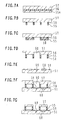
- Figs. 7A to 7G are schematic cross sectional views illustrating a solid state image pickup device using a wafer level chip size packaging (CSP) process.
- CSP wafer level chip size packaging
- FIG. 7A A protective glass 57 and a silicon substrate 55a are bonded together with adhesive 56 of, for example, an ultraviolet ray curing type. Spacers are formed by using the silicon substrate 55a in the next process.
- Resist patterns are formed on the silicon substrate 55a by photolithography in the areas where spacers are to be formed.
- the silicon substrate 55a is then etched to form spacers 55.
- Fig. 7C The regions between spacers 55 excepting the regions between devices are filled with resist 58, and the protective glass 57 is etched to a predetermined depth.
- Fig. 7D The etched region of the protective glass 57 constitutes an inter-device groove 60.
- Adhesive 54 of, for example, a thermosetting type is coated on the bottoms of the spacers 55. With the processes shown in Figs. 7A to 7D, a sealing cover glass is formed.
- a solid state image pickup device substrate is formed.
- a cut groove 69 is formed in the surface layer of the silicon substrate 51 by etching or the like, in the area corresponding to a dicing line for separating the substrate into each semiconductor chip.
- a solid state image pickup device 68 is formed by ordinary silicon processes.
- a wiring layer is formed on the substrate surface, and pads 59 of metal material for external connection are formed.
- Fig. 7F Position alignment is performed and the sealing cover glass is placed on the solid state image pickup device substrate.
- the sealing glass cover and substrate are integrally bonded with heated adhesive 54.
- This process is preferably executed in a vacuum state, a nitrogen gas atmosphere or an inert gas atmosphere, or in an atmosphere of nitrogen gas or inert gas mixed with some air.
- Fig. 7G The upper side of the protective glass 57 is removed down to the inter-device groove 60 by chemical mechanical polishing (CMP).
- CMP chemical mechanical polishing
- the bottom side of the silicon substrate is removed up to the cut groove 69 by CMP to separate the substrate into each semiconductor chip.
- It is an object of at least the preferred embodiments of this invention is to provide a solid state image pickup device having high resistance against electrostatic breakdown.
- Another object of at least the preferred embodiments of this invention is to provide an endoscope having high resistance against electrostatic breakdown.
- a solid state image pickup device comprising: a semiconductor substrate of a first conductivity type; a well of a second conductivity type opposite to the first conductivity type formed in a surface layer of the semiconductor substrate; a light reception region formed in the well and including a plurality of charge accumulation regions of the first conductivity type formed in a matrix shape for accumulating signal charges generated in correspondence with an amount of incidence light and a plurality of vertical CCDs formed along each column of the charge accumulation regions for reading the signal charges accumulated in the charge accumulation regions and transferring the signal charges in a column direction; a horizontal CCD formed in the well and coupled to ends of the vertical CCDs for transferring the signal charges transferred from the vertical CCDs; a peripheral circuit formed in the well in partial regions of the light reception region and the horizontal CCD; a shield layer formed on the semiconductor substrate including a partial area above the peripheral circuit, made of conductive material and surrounding the light reception region, the shield layer being electrically connected to the semiconductor substrate of the first conductivity
- This solid state image pickup device has a high electrostatic breakdown resistance and high quality capable of preventing devices such as an input/output protective circuit and a wiring portion from being broken, even if a strong electric field is generated between the bottom surface of the support and the semiconductor substrate due to static electricity generated, for example, on the translucent member.
- an endoscope comprising: a light source for emitting light; a solid state image pickup device including a semiconductor substrate of a first conductivity type, a well of a second conductivity type opposite to the first conductivity type formed in a surface layer of the semiconductor substrate, a light reception region formed in the well and including a plurality of charge accumulation regions of the first conductivity type formed in a matrix shape for accumulating signal charges generated in correspondence with an amount of incidence light and a plurality of vertical CCDs formed along each column of the charge accumulation regions for reading the signal charges accumulated in the charge accumulation regions and transferring the signal charges in a column direction, a horizontal CCD formed in the well and coupled to ends of the vertical CCDs for transferring the signal charges transferred from the vertical CCDs, a peripheral circuit formed in the well in partial regions of the light reception region and the horizontal CCD, a shield layer formed on the semiconductor substrate including a partial area above the peripheral circuit, made of conductive material and surrounding the light reception region, the shield layer being
- This endoscope using the above-described solid state image pickup device has a high quality and can prevent breakage of a device such as an input/output protective circuit and a wiring portion.
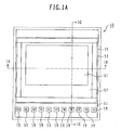
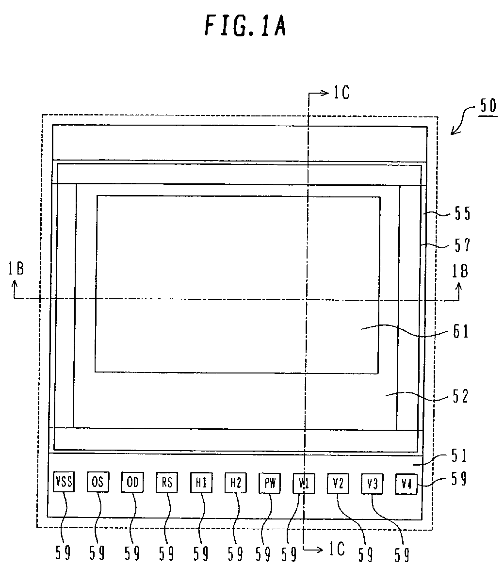
- Fig. 1A is a schematic plan view showing an example of a semiconductor chip 50 formed with a solid state image pickup device whose light reception region is protected with a protective glass, and Figs. 1B and 1C are cross sectional views taken along respective lines 1B-1B and 1C-1C shown in Fig. 1A;
- Fig. 2 is a schematic cross sectional plan view of a solid state image pickup device according to an embodiment
- Figs. 3A and 3B are schematic plan views showing the structure of CCD solid state image pickup devices
- Fig. 3C is a schematic cross sectional view showing a partial region of a light reception region of a CCD solid state image pickup device
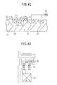
- Figs. 4A to 4D are diagrams illustrating a peripheral area (an input/output protective circuit and the like under a shield layer 90) of a silicon substrate and a spacer 55;
- Figs. 5A and 5B are schematic cross sectional views showing the region near the shield layer 90;
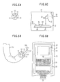
- Fig. 6A is a schematic plan view showing a tip portion of an upper digestive tract fine inspection optical magnification electron scope (endoscope)
- Fig. 6B is a perspective view of the tip portion of the scope and a tube near the tip portion
- Figs. 6C and 6D are schematic diagrams illustrating an observation optical system of the scope
- Figs. 7A to 7G are schematic cross sectional views illustrating a solid state image pickup device manufacture method using a wafer level CSP process.
- Fig. 1A is a schematic plan view showing an example of a semiconductor chip 50 formed with a solid state image pickup device whose light reception region is protected with a protective glass.
- Figs. 1B and 1C are cross sectional views taken along respective lines 1B-1B and 1C-1C shown in Fig. 1A.
- the semiconductor chip 50 includes a silicon substrate 51, a semiconductor device 52 formed on the silicon substrate 51, a spacer (support member) 55 formed on the semiconductor device 52, a protective glass 57 adhered to the spacer 55, and a plurality of pads 59 formed in the peripheral area of the silicon substrate 51.
- the semiconductor device 52 includes a solid state image pickup device and its peripheral circuit (e.g., an input/output protective circuit for protecting an internal circuit from an external surge voltage, and a wiring portion such as outer peripheral wirings).
- a portion formed near the surface of the silicon substrate 51 is called a semiconductor device 52.
- the spacer 55 made of conductive material such as silicon is formed on the semiconductor device 52, with an insulating film being interposed therebetween.
- the spacer 55 is formed surrounding the outer periphery of the light reception region 61 of the solid state image pickup device, as viewed in plan.
- a translucent member such as protective glass 57 is placed on the spacer 55.
- the protective glass 57 protects the solid state image pickup device from moisture and mechanical factors.
- the semiconductor chip 50 can be manufactured by forming a number of semiconductor devices 52 on a silicon wafer and dicing the wafer into separate semiconductor devices 52. Dust formed during the manufacture processes, especially during processes after the dicing process, is prevented from attaching the light reception region 61 by the protective glass 57.
- Plural pads 59 are external connection terminals for electrical connection between the semiconductor chip 50 and a circuit board on which drive circuits, wirings and the like are formed.
- the semiconductor device 52 is formed by processing the silicon substrate 51 through ion implantation and the like.
- a passivation film 53 having a thickness of, e.g., 2 ⁇ m, is formed on the semiconductor device 52.
- the spacer 55 having a thickness of, e.g., 100 ⁇ m, is bonded to the passivation film 53 with epoxy-resin based adhesive 54.
- a thickness of the adhesive 54 is, for example, 2 ⁇ m.
- each pad 59 is used for electrical connection (wire bonding) between the semiconductor chip 50 and an external wiring substrate.
- Each pad 59 is formed at a position where a capillary of a bonder does not contact the protective glass 57 during wire bonding. This is because the protective glass 57 may be broken if the capillary contacts the protective glass 57. Therefore, the pad 59 is formed at the position spaced by a predetermined distance from the end of the protective glass 57.
- the present inventor has proposed various approaches (e.g., refer to Claims and paragraphs [0041] to [0079] of Best Mode for Carrying Out the Invention in Specification of Japanese Patent Application No. 2004-183868 ).
- a solid state image pickup device having a width of 2 mm and 0.17 million pixels was manufactured in order to narrowing a transmission tube of an endoscope.
- the spacer 55 is formed above a partial region of the peripheral circuit (input/output protective circuit or the like, or a wiring portion such as outer peripheral wirings or the like). Some phenomena occurred such as malfunction of an input/output protective circuit or a wiring portion such as an outer peripheral wiring portion).
- the input/output protective circuit and wiring portion are positioned lower than, for example, by 1 to 5 ⁇ m from the surface (uppermost surface) of the semiconductor device 52, and near at, for example, 2 to 10 ⁇ m from the bottom surface of the spacer 55.
- the semiconductor chip 50 having the structure that the light reception region 61 of the solid state image pickup device is covered with the protective glass 57 placed on the spacer 55 is to be manufactured, as described with reference to Figs. 7A to 7G, in many cases, first the spacer 55 and protective glass 57 are bonded together and thereafter the protective glass 57 is bonded to the semiconductor device 52 via the spacer 55. These processes are performed relative to a silicon wafer, and each semiconductor chip 50 with the semiconductor device 52 is formed by dicing the wafer.
- Static electricity is generated in some cases on the surface of the protective glass 57, during a bonding process for the spacer 55 and protective glass 57, during a bonding process for the spacer 55 bonded to the protective glass 57 and the semiconductor device 52 or during a dicing process.
- a ceramic package has a distance of several hundred ⁇ m between the lower surface of the protective glass at the upper surface of the package and the input/output protective circuit and wiring portion of the semiconductor device. This distance causes an electric field due to static electricity to have an intensity weaker by about two orders of magnitude than that of the semiconductor chip having the structure that the light reception region of the solid state image pickup device is covered with the protective glass placed on the spacer.
- the present inventor has devised a solid state image pickup device and an endoscope having a novel structure.
- Fig. 2 is a schematic cross sectional view of a solid state image pickup device according to an embodiment.
- a semiconductor device 52 is formed on a silicon substrate 51.
- the semiconductor device 52 includes a solid state image pickup device and its peripheral circuit (e.g., an input/output protective circuit and a wiring portion such as outer peripheral wirings).
- the spacer 55 is disposed surrounding the periphery of the light reception region of the solid state image pickup device as viewed in plan (as the semiconductor device 52 is viewed from the position of the protective glass 57). Therefore, the shield layer 90 under the spacer 55 is also formed surrounding the periphery of the light reception region.
- a translucent member e.g., the protective glass 57, is placed on the spacer 55.
- Pads 59 are formed on the silicon substrate 51 for electrical connection to an external wiring substrate.
- An insulating layer is formed between the semiconductor device 52 and shield layer 90 and between the shield layer 90 and spacer 55.
- the shield layer 90 is electrically connected to the n-type silicon substrate 51 and is conductive to the bottom surface of the silicon substrate 51 at low resistance.
- the shield layer 90 and silicon substrate 51 (at the bottom surface thereof) have therefore generally the same potential.
- the bottom surface of the silicon substrate 51 is electrically connected to an external apparatus.
- FIGS. 3A and 3B are schematic plan views showing the structure of CCD solid state image pickup devices
- Fig. 3C is a schematic cross sectional view showing a partial region of a light reception region of a CCD solid state image pickup device.
- a CCD solid state image pickup device is constituted of: a plurality of photosensitive regions 62 disposed, for example, in a square matrix shape; a plurality of vertical transfer channels (vertical CCDs) 64 disposed along columns of the photosensitive regions 62; a horizontal transfer channel (horizontal CCD) 66 electrically connected to the ends of the vertical transfer channels 64 outside a light reception region (pixel array region) 61; and a charge detection unit 67 coupled to one end of the horizontal transfer channel 66.
- the light reception region 61 is constituted of the photosensitive regions 62 and vertical transfer channels 64.
- the photosensitive region 62 is constituted of a photosensitive element, e.g., a photodiode, and a transfer gate.
- the photodiode generates and accumulates signal charges corresponding to an incidence light amount.
- the accumulated signal charges are read to the vertical transfer channels 64 via transfer gates and transferred in the vertical transfer channels 64 along a direction (vertical direction, column direction) toward the horizontal transfer channel 66 as a whole. Signal charges transferred to the ends of the vertical transfer channels 64 are transferred into the horizontal transfer channel 66.
- Signal charges transferred into the horizontal transfer channel 66 are transferred in the horizontal transfer channel 66 along a direction crossing the vertical direction as a whole, e.g., a horizontal direction (direction perpendicular to the vertical direction, row direction), and thereafter transferred to the charge detection unit 67.
- the charge detection unit 67 performs charges-voltage conversion and signal amplification.
- the amplified image signal is delivered to the outside.
- the array of photosensitive regions 62 includes a square array and a rectangle array with the photosensitive regions being disposed along the row and column directions at constant pitches as shown in Fig. 3A, and in addition, a pixel interleaved array (PIA) having pixels disposed along the row and column directions by shifting the pixels, for example, a half pitch at every second rows and columns.
- PPA pixel interleaved array
- Fig. 3B is a schematic plan view of a CCD solid state image pickup device of the pixel interleaved array.
- the pixel interleaved array is an array of photosensitive regions disposed in a first square matrix shape and photosensitive regions disposed in a second square matrix shape at positions between lattice points of the first square matrix shape.
- the vertical transfer channel 64 is formed in a zigzag shape between photosensitive regions 62. Also in this case, signal charges are transferred in the vertical transfer channel 64 along a direction (vertical direction) toward the horizontal transfer channel 66 as a whole.
- the photosensitive region 62 in the pixel interleaved array is of an octagonal shape in many cases.
- Fig. 3C is a schematic cross sectional view showing a partial region of the light reception region of a CCD solid state image pickup device.
- a charge accumulation region 71 made of an n-type impurity doped region and a vertical transfer channel 64 made of an n-type impurity region being adjacent to a plurality of charge accumulation regions and via a p-type transfer gate 72.
- a photodiode is constituted of the n-type charge accumulation region 71 and underlying p-type well 82.
- a vertical transfer electrode 75 is formed above the transfer gate 72 and vertical transfer channel 64, with an insulating film 74 being interposed therebetween.
- a p-type channel stopper region 76 is formed between adjacent charge accumulation regions 71.
- the channel stop region 76 electrically isolates the charge accumulation region 71, vertical transfer channel 64 and the like.
- the insulating film 74 is, for example, a lamination structure (ONO film) of an oxide film, a nitride film and an oxide film, formed on the surface of the silicon substrate 51.
- the vertical transfer electrode 75 includes a first vertical transfer electrode and a second vertical transfer electrode made of, for example, polysilicon. These electrodes may be made of amorphous silicon.
- the vertical transfer electrode 75 controls the potentials of the vertical transfer channel 64 and transfer gate 72 to read charges accumulated in the charge accumulation region 71 to the vertical transfer channel 64 and transfer the read charges in the vertical transfer channel 64 along the column direction.
- An insulating silicon oxide film 77 formed, for example, by thermally oxidizing polysilicon is formed on the vertical transfer electrode 75.
- An opening 79a is formed through the light shielding film 79 above the charge accumulation region 71.
- the light shielding film 79 prevents incidence light upon the light reception region 61 from entering the region other than the charge accumulation region 71.
- a silicon nitride film 78 is formed on the light shielding film 79.
- another planarizing layer 83b is formed.
- Micro lenses 85 are formed on a flat surface of the planarizing layer 83b, for example, by melting and solidifying a micro lens photoresist pattern.
- the micro lenses 85 are an array of, e.g., fine semispherical convex lenses disposed above the charge accumulation regions 71.
- Each micro lens 85 converges incidence light on the charge accumulation region 71.
- Light converged by each micro lens passes through the color filter layer 84 of one of red (R), green (G) and blue (B) and becomes incident upon the corresponding charge accumulation region (photodiode) 71.
- a plurality of photodiodes include therefore three types of photodiodes: a photodiode upon which light transmitted through the red (R) color filter layer 84 becomes incident; a photodiode upon which light transmitted through the green (G) color filter layer 84 becomes incident; and a photodiode upon which light transmitted through the blue (B) color filter layer 84 becomes incident.
- Signal charges accumulated in the charge accumulation region 71 and corresponding in amount to an incidence light amount are read to the vertical transfer channel 64 by a drive signal (read voltage) applied to the vertical transfer electrode 75 above the transfer gate 72, and transferred in the vertical transfer channel 64 by a drive signal (transfer voltage) applied to the vertical transfer electrode 75.
- Fig. 4A an area of the silicon substrate where a peripheral circuit is formed is surrounded by a broken line and hatched.
- an input/output protective circuit is formed in a large area and only a portion thereof exists under the spacer in some cases.
- a plurality of pads 59 to be used for connection to an external wiring substrate include a supply voltage terminal (ground terminal) VSS, an output voltage terminal OS, a supply voltage terminal OD, a reset pulse voltage terminal RS, horizontal transfer electrode drive signal terminals H1 and H2, a protector/well voltage terminal PW and vertical transfer electrode drive signal terminals V1 to V4.
- VSS, OD and PW are not provided with a protective circuit, whereas V1 to V4 are connected to PW via a protective circuit and H1, H2 and RS are connected to VSS via a protective circuit.
- Fig. 4B is an equivalent circuit of the protective circuit.
- a pad 59 is electrically connected to a solid state image pickup device via a protective resistor 95, and to a VSS or PW pad 59 via a parallel circuit of a metal gate transistor 96 and a diode 97, between the protective resistor and solid state image pickup device.
- the diode 97 turns on so that the surge voltage is absorbed in VSS or PW and the circuit in the solid state image pickup device can be protected.
- the metal gate field transistor 96 turns on so that the surge voltage is absorbed in VSS or PW and the circuit in the solid state image pickup device can be protected.
- Fig. 4C shows an embodiment of the protective circuit shown in Fig. 4B.
- An SiO 2 layer (isolation region) 91 is formed on the surface of an n-type silicon substrate 51.
- a p-type well 82 having an edge defined under the SiO 2 layer 91 is formed in the surface layer of the silicon substrate 51.
- a high concentration p-type impurity layer 30 is formed in the p-type well 82 on one side of the SiO 2 layer 91, and a drain/gate electrode 33 is formed on the high concentration p-type impurity layer 30 and SiO 2 layer 91.
- a high concentration p-type impurity layer 31 is formed in the surface layer of the silicon substrate 51 on the other side of the SiO 2 layer 91 opposite to the high concentration p-type impurity layer 30.
- a high concentration n-type impurity layer 32 is formed in the surface layer of the silicon substrate 51.
- the high concentration p-type impurity layer 31 and high concentration n-type impurity layer 32 are connected in common to the pad 59.
- the high concentration n-type impurity layer 32, n-type silicon substrate 51 and p-type well 82 constitute the diode 97.
- the metal gate field transistor 96 is formed by using the high concentration p-type impurity layer 31 as a source, the high concentration p-type impurity layer 30 and p-type well 82 as a drain, the n-type region under the SiO 2 layer 91 as a channel and the electrode on the SiO 2 layer 91 as a gate.
- Fig. 4D shows an example of the protective circuit near the pad 59 H1 shown in Fig. 4A.
- the protective circuit is constituted of the protective resistor 95 and metal gate field transistor 96 shown in Fig. 4B.
- the shield layer and spacer are formed, for example, above the metal gate field transistor 96 of the protective circuit 96 to protect the protective circuit from electrostatic breakage.
- Figs. 5A and 5B are schematic cross sectional views showing the region near the shield layer 90.
- Fig. 5A is a cross sectional view showing the region with the polysilicon layer constituting the gate electrode
- Fig. 5B is a cross sectional view showing the region with the source/drain Al electrode instead of the gate electrode.
- a peripheral circuit of a semiconductor device e.g., the input/output protective circuit described with reference to Figs. 4B to 4D, is formed in a p-type well 82 formed in a surface layer of an n-type silicon substrate 51.
- the peripheral circuit is formed in the p-type well 82 in the light reception region of a solid state image pickup device and a peripheral area of the horizontal CCD.
- An SiO 2 layer (isolation region) 91 as an insulating layer is formed on the surface of the well layer 82.
- an Al layer 92 constituting a source/drain electrode and a polysilicon layer 93 constituting a gate electrode are formed in an active region defined by the SiO 2 layer 91.
- the Al layer 92 is electrically connected to the well 82 to form a well contact.
- a shield layer 90 made of, for example, Al is formed above the Al layer 92.
- the shield layer 90 is electrically connected to the n-type silicon substrate 51 at a position where the well 82 is not formed, to form a substrate contact 94.
- a passivation film 53a is used for electrical insulation of the gate electrode, and a passivation film 53b is used for electrical insulation of the Al layer 92.
- a passivation film 53c is formed on the shield layer 90, and a spacer is formed above the passivation film.
- the shield layer 90 is made conductive with the silicon substrate 51.
- this voltage can be absorbed. Namely, this voltage is applied not to the device but to the shield layer electrically connected to the silicon substrate. This voltage can be applied to an external of the semiconductor chip via the shield layer 90 and silicon substrate 51. It is therefore possible to protect the semiconductor device (input/output protective circuit, wiring portion and the like) from electrostatic breakdown.
- a solid state image pickup device having a high static electricity resistance and high quality can therefore be realized even if the structure that a protective glass is disposed only in the light reception region, which is advantageous in compactness of a semiconductor chip, is adopted.
- the shield layer 90 may be made of the same metal layer as that of the light shielding film 79 shown in Fig. 2C.
- a compact and high quality endoscope can be realized by using the above-described solid state image pickup device.
- Fig. 6A is a schematic plan view showing a tip portion of an upper digestive tract fine inspection optical magnification electron scope (endoscope)
- Fig. 6B is a perspective view of the tip portion of the scope and a tube near the tip portion
- Figs. 6C and 6D are schematic diagrams illustrating an observation optical system of the scope.
- the tip portion of an upper digestive tract fine inspection optical magnification electron scope (endoscope) has generally a circular shape of 6.0 mm diameter and is constituted of a light source 11, an observation optical system 12, a nozzle 13 and a forceps opening 14.
- the light source 11 shown in Fig. 6A corresponds to an outlet port for the light source including a light emission source, a light guide (fiber) and the outlet port.
- the electron scope is used, for example, as a photogastroscope.
- the light source 11 is formed at two positions of the tip portion, emits, for example, white light whose infrared range is cut, and illuminates an organism such as a human gastric wall.
- the observation optical system 12 is constituted of a solid state image pickup device like the embodiment solid state image pickup device, forms an image mainly by receiving light emitted from the light source and reflected from the gastric wall, and transmits the image to an observer.
- the observation optical system 12 will be later detailed.
- the nozzle 13 is an output port which jets out air or liquid, for example, wash or stain.
- the forceps opening 14 is an inlet/outlet port of forceps.
- the forceps opening has a diameter of, for example, 2.8 mm.
- a pair of forceps 14a is pulled out or in through the forceps opening 14.
- the forceps 14a perform an open/close operation at its tip portion like blades of a pair of scissors, and can grip or squeeze an object. By operating the forceps 14a, it is possible to observe a disease portion in detail and pick up cells of the disease portion.
- the light source (outlet port) 11, observation optical system 12, nozzle 13 and forceps opening 14 (forceps 14a) are disposed in the tube 15, e.g., near at the tip portion of the tube.
- the tube 15 is introduced into the body via, for example, a nostril to make the tip portion reach near the disease portion. If the tube is introduced not via a mouth but via a nostril, a patient can be inspected while a conversation with the patient is made.
- a scope to be introduced via a nostril has a smaller diameter than that of a scope to be introduced via a mouth.
- a portion near the tip portion of the tube 15 is made flexible so that the operation of the scope such as moving the observation optical system 12 and the like nearer to the disease portion can be improved.
- a total length of the tube 15 is, for example, 1400 mm.
- the tube 15 is provided with a control device at the end of the tube opposite to the position where the observation optical system 12 and the like are disposed.
- the control device can operate the light source 11, observation optical system 12, nozzle 13 and forceps 14a.
- Image data from the observation optical system 12 is transmitted in the tube 15 to an external.
- the tube 15 is a mechanical and electrical transmission tube.
- the observation optical system 12 is constituted of an objective lens 21, a prism 22, a semiconductor chip 50 and a wiring substrate 26.
- the embodiment solid state image pickup device and pads 59 are formed on the semiconductor chip 50.
- Pads 24 of the wiring substrate 26, on which wirings such as those of a drive circuit are formed, are wire-bonded to the pads 59 of the semiconductor chip 50.
- Leads 25 from the wiring substrate 26 extend in the tube 15 along the extension direction of the tube 15.
- the semiconductor chip 50 and wiring substrate 26 are supported on a support plate 27.
- Fig. 6D Light 20 incident upon the objective lens 21 being changed its propagation direction by the prism 22 becomes incident upon a plurality of photoelectric conversion elements in the light reception region 61 of the solid state image pickup device of the semiconductor chip 50 so that signal charges are generated and accumulated. After the signal charges are transferred in the solid state image pickup device, the charges are output as image data. The image data is output to the outside via leads 25.
- the semiconductor chip 50 is disposed in such a manner that its principal surface (surface on which the photoelectric conversion elements are formed) of, e.g., a rectangular shape, is perpendicular to the cross section of the tube 15 and a longitudinal direction of the principal surface is parallel to the extension direction of the tube 15. With this arrangement, the scope can be made compact. Changing the propagation direction of incidence light by the prism 22 is intended to make the scope compact by disposing the principal surface of the semiconductor chip 50 perpendicular to the cross section of the tube 15.
- the semiconductor chip 50 is disposed in such a manner that its upper side (on the side of the light reception region 61) is positioned near to the objective lens 21. Therefore, light to become incident upon the objective lens 21 before the light is reflected by the prism 22 propagates along a direction from the light reception region 61 toward the horizontal transfer channel and pads 59 (in a direction of transferring signal charges in the vertical transfer channel in the light reception region 61 as a whole).
- the endoscope shown in Figs. 6A to 6D uses the embodiment of the solid state image pickup device, the endoscope is compact and has a high static electricity resistance and high quality.
- an industrial endoscope can be realized which is compact and has a high static electricity resistance and high quality.
- the present invention is particularly suitable for application to a solid state image pickup device and an endoscope to be used for the fields where compactness requirements are severe.
Landscapes
- Health & Medical Sciences (AREA)
- Life Sciences & Earth Sciences (AREA)
- Surgery (AREA)
- Engineering & Computer Science (AREA)
- Radiology & Medical Imaging (AREA)
- Heart & Thoracic Surgery (AREA)
- Biophysics (AREA)
- Nuclear Medicine, Radiotherapy & Molecular Imaging (AREA)
- Optics & Photonics (AREA)
- Pathology (AREA)
- Veterinary Medicine (AREA)
- Public Health (AREA)
- Biomedical Technology (AREA)
- Physics & Mathematics (AREA)
- Medical Informatics (AREA)
- Molecular Biology (AREA)
- Animal Behavior & Ethology (AREA)
- General Health & Medical Sciences (AREA)
- Multimedia (AREA)
- Signal Processing (AREA)
- Endoscopes (AREA)
- Solid State Image Pick-Up Elements (AREA)
- Transforming Light Signals Into Electric Signals (AREA)
Abstract

Description
- The present invention relates to a solid state image pickup device and an endoscope using a solid state image pickup device.
- Various structures and manufacture methods are known for a solid state image pickup device (semiconductor chip) whose light reception region is protected with a protective glass (e.g., refer to
Japanese Patent Laid-open Publication No. 2004-6834 - Figs. 7A to 7G are schematic cross sectional views illustrating a solid state image pickup device using a wafer level chip size packaging (CSP) process.
- Reference is made to Fig. 7A. A
protective glass 57 and asilicon substrate 55a are bonded together with adhesive 56 of, for example, an ultraviolet ray curing type. Spacers are formed by using thesilicon substrate 55a in the next process. - Reference is made to Fig. 7B. Resist patterns are formed on the
silicon substrate 55a by photolithography in the areas where spacers are to be formed. Thesilicon substrate 55a is then etched to formspacers 55. - Reference is made to Fig. 7C. The regions between
spacers 55 excepting the regions between devices are filled with resist 58, and theprotective glass 57 is etched to a predetermined depth. - Reference is made to Fig. 7D. The etched region of the
protective glass 57 constitutes aninter-device groove 60. Adhesive 54 of, for example, a thermosetting type is coated on the bottoms of thespacers 55. With the processes shown in Figs. 7A to 7D, a sealing cover glass is formed. - Reference is made to Fig. 7E. Next, a solid state image pickup device substrate is formed.
- First, a
cut groove 69 is formed in the surface layer of thesilicon substrate 51 by etching or the like, in the area corresponding to a dicing line for separating the substrate into each semiconductor chip. Next, a solid stateimage pickup device 68 is formed by ordinary silicon processes. A wiring layer is formed on the substrate surface, and pads 59 of metal material for external connection are formed. - Reference is made to Fig. 7F. Position alignment is performed and the sealing cover glass is placed on the solid state image pickup device substrate. The sealing glass cover and substrate are integrally bonded with heated
adhesive 54. This process is preferably executed in a vacuum state, a nitrogen gas atmosphere or an inert gas atmosphere, or in an atmosphere of nitrogen gas or inert gas mixed with some air. - Reference is made to Fig. 7G. The upper side of the
protective glass 57 is removed down to theinter-device groove 60 by chemical mechanical polishing (CMP). The bottom side of the silicon substrate is removed up to thecut groove 69 by CMP to separate the substrate into each semiconductor chip. - It is an object of at least the preferred embodiments of this invention is to provide a solid state image pickup device having high resistance against electrostatic breakdown.
- Another object of at least the preferred embodiments of this invention is to provide an endoscope having high resistance against electrostatic breakdown.
- According to a first aspect of the present invention, there is provided a solid state image pickup device comprising: a semiconductor substrate of a first conductivity type; a well of a second conductivity type opposite to the first conductivity type formed in a surface layer of the semiconductor substrate; a light reception region formed in the well and including a plurality of charge accumulation regions of the first conductivity type formed in a matrix shape for accumulating signal charges generated in correspondence with an amount of incidence light and a plurality of vertical CCDs formed along each column of the charge accumulation regions for reading the signal charges accumulated in the charge accumulation regions and transferring the signal charges in a column direction; a horizontal CCD formed in the well and coupled to ends of the vertical CCDs for transferring the signal charges transferred from the vertical CCDs; a peripheral circuit formed in the well in partial regions of the light reception region and the horizontal CCD; a shield layer formed on the semiconductor substrate including a partial area above the peripheral circuit, made of conductive material and surrounding the light reception region, the shield layer being electrically connected to the semiconductor substrate of the first conductivity type; a support disposed above the shield layer and made of conductive material; and a translucent member placed on the support.
- This solid state image pickup device has a high electrostatic breakdown resistance and high quality capable of preventing devices such as an input/output protective circuit and a wiring portion from being broken, even if a strong electric field is generated between the bottom surface of the support and the semiconductor substrate due to static electricity generated, for example, on the translucent member.
- According to another aspect of the present invention, there is provided an endoscope comprising: a light source for emitting light; a solid state image pickup device including a semiconductor substrate of a first conductivity type, a well of a second conductivity type opposite to the first conductivity type formed in a surface layer of the semiconductor substrate, a light reception region formed in the well and including a plurality of charge accumulation regions of the first conductivity type formed in a matrix shape for accumulating signal charges generated in correspondence with an amount of incidence light and a plurality of vertical CCDs formed along each column of the charge accumulation regions for reading the signal charges accumulated in the charge accumulation regions and transferring the signal charges in a column direction, a horizontal CCD formed in the well and coupled to ends of the vertical CCDs for transferring the signal charges transferred from the vertical CCDs, a peripheral circuit formed in the well in partial regions of the light reception region and the horizontal CCD, a shield layer formed on the semiconductor substrate including a partial area above the peripheral circuit, made of conductive material and surrounding the light reception region, the shield layer being electrically connected to the semiconductor substrate of the first conductivity type, a support disposed above the shield layer and made of conductive material, and a translucent member placed on the support; and a transmission tube having therein the light source and the solid state image pickup device.
- This endoscope using the above-described solid state image pickup device has a high quality and can prevent breakage of a device such as an input/output protective circuit and a wiring portion.
- According to the first aspect of the present invention, it is possible to provide a solid state image pickup device having high resistance against electrostatic breakdown.
- According to the second aspect of the present invention, it is possible to provide an endoscope having high resistance against electrostatic breakdown.
- Preferred embodiments of the invention will now be described by way of example only and with reference to the accompanying drawings, in which:
- Fig. 1A is a schematic plan view showing an example of a
semiconductor chip 50 formed with a solid state image pickup device whose light reception region is protected with a protective glass, and Figs. 1B and 1C are cross sectional views taken along respective lines 1B-1B and 1C-1C shown in Fig. 1A; - Fig. 2 is a schematic cross sectional plan view of a solid state image pickup device according to an embodiment;
- Figs. 3A and 3B are schematic plan views showing the structure of CCD solid state image pickup devices, and Fig. 3C is a schematic cross sectional view showing a partial region of a light reception region of a CCD solid state image pickup device;
- Figs. 4A to 4D are diagrams illustrating a peripheral area (an input/output protective circuit and the like under a shield layer 90) of a silicon substrate and a
spacer 55; - Figs. 5A and 5B are schematic cross sectional views showing the region near the
shield layer 90; - Fig. 6A is a schematic plan view showing a tip portion of an upper digestive tract fine inspection optical magnification electron scope (endoscope), Fig. 6B is a perspective view of the tip portion of the scope and a tube near the tip portion, and Figs. 6C and 6D are schematic diagrams illustrating an observation optical system of the scope; and
- Figs. 7A to 7G are schematic cross sectional views illustrating a solid state image pickup device manufacture method using a wafer level CSP process.
- As mentioned above, Fig. 1A is a schematic plan view showing an example of a
semiconductor chip 50 formed with a solid state image pickup device whose light reception region is protected with a protective glass. Figs. 1B and 1C are cross sectional views taken along respective lines 1B-1B and 1C-1C shown in Fig. 1A. - The
semiconductor chip 50 includes asilicon substrate 51, asemiconductor device 52 formed on thesilicon substrate 51, a spacer (support member) 55 formed on thesemiconductor device 52, aprotective glass 57 adhered to thespacer 55, and a plurality ofpads 59 formed in the peripheral area of thesilicon substrate 51. - The
semiconductor device 52 includes a solid state image pickup device and its peripheral circuit (e.g., an input/output protective circuit for protecting an internal circuit from an external surge voltage, and a wiring portion such as outer peripheral wirings). For the purposes of simplicity, a portion formed near the surface of thesilicon substrate 51 is called asemiconductor device 52. - The
spacer 55 made of conductive material such as silicon is formed on thesemiconductor device 52, with an insulating film being interposed therebetween. Thespacer 55 is formed surrounding the outer periphery of thelight reception region 61 of the solid state image pickup device, as viewed in plan. - A translucent member such as
protective glass 57 is placed on thespacer 55. Theprotective glass 57 protects the solid state image pickup device from moisture and mechanical factors. Thesemiconductor chip 50 can be manufactured by forming a number ofsemiconductor devices 52 on a silicon wafer and dicing the wafer intoseparate semiconductor devices 52. Dust formed during the manufacture processes, especially during processes after the dicing process, is prevented from attaching thelight reception region 61 by theprotective glass 57. -
Plural pads 59 are external connection terminals for electrical connection between thesemiconductor chip 50 and a circuit board on which drive circuits, wirings and the like are formed. - Reference is made to Fig. 1B. The
semiconductor device 52 is formed by processing thesilicon substrate 51 through ion implantation and the like. Apassivation film 53 having a thickness of, e.g., 2 µm, is formed on thesemiconductor device 52. Thespacer 55 having a thickness of, e.g., 100 µm, is bonded to thepassivation film 53 with epoxy-resin basedadhesive 54. A thickness of the adhesive 54 is, for example, 2 µm. - The
protective glass 57 having a thickness of, e.g., 250 µm, is bonded to thespacer 55 withadhesive 56 of an ultraviolet curing type. - Reference is made to Fig. 1C. As described earlier, each
pad 59 is used for electrical connection (wire bonding) between thesemiconductor chip 50 and an external wiring substrate. Eachpad 59 is formed at a position where a capillary of a bonder does not contact theprotective glass 57 during wire bonding. This is because theprotective glass 57 may be broken if the capillary contacts theprotective glass 57. Therefore, thepad 59 is formed at the position spaced by a predetermined distance from the end of theprotective glass 57. - In order to meet compactness requirements of the
semiconductor chip 50, the present inventor has proposed various approaches (e.g., refer to Claims and paragraphs [0041] to [0079] of Best Mode for Carrying Out the Invention in Specification ofJapanese Patent Application No. 2004-183868 spacer 55 is formed above a partial region of the peripheral circuit (input/output protective circuit or the like, or a wiring portion such as outer peripheral wirings or the like). Some phenomena occurred such as malfunction of an input/output protective circuit or a wiring portion such as an outer peripheral wiring portion). - According to the studies by the present inventor, the input/output protective circuit and wiring portion are positioned lower than, for example, by 1 to 5 µm from the surface (uppermost surface) of the
semiconductor device 52, and near at, for example, 2 to 10 µm from the bottom surface of thespacer 55. - When the
semiconductor chip 50 having the structure that thelight reception region 61 of the solid state image pickup device is covered with theprotective glass 57 placed on thespacer 55 is to be manufactured, as described with reference to Figs. 7A to 7G, in many cases, first thespacer 55 andprotective glass 57 are bonded together and thereafter theprotective glass 57 is bonded to thesemiconductor device 52 via thespacer 55. These processes are performed relative to a silicon wafer, and eachsemiconductor chip 50 with thesemiconductor device 52 is formed by dicing the wafer. - Static electricity is generated in some cases on the surface of the
protective glass 57, during a bonding process for thespacer 55 andprotective glass 57, during a bonding process for thespacer 55 bonded to theprotective glass 57 and thesemiconductor device 52 or during a dicing process. - As static electricity is generated on the surface of the
protective glass 57, charges having an opposite polarity are generated on the bottom surface of theprotective glass 57. Since thespacer 55 made of conductor exists between the bottom surface of theprotective glass 57 and thesemiconductor device 52, a strong electric field caused by the static electricity is generated in a narrow region from the bottom surface of thespacer 55 to the input/output protective circuit and wiring portion, for example, having a distance of 2 to 10 µm. The present inventor has considered that this strong electric field causes electrostatic breakage of the input/output protective circuit and wiring portion, resulting in a malfunction of circuit operation. - Malfunction of circuit operation is hard to occur in a widely used ceramic package. This may be ascribed to that a ceramic package has a distance of several hundred µm between the lower surface of the protective glass at the upper surface of the package and the input/output protective circuit and wiring portion of the semiconductor device. This distance causes an electric field due to static electricity to have an intensity weaker by about two orders of magnitude than that of the semiconductor chip having the structure that the light reception region of the solid state image pickup device is covered with the protective glass placed on the spacer.
- Based on these studies, the present inventor has devised a solid state image pickup device and an endoscope having a novel structure.
- Fig. 2 is a schematic cross sectional view of a solid state image pickup device according to an embodiment.
- A
semiconductor device 52 is formed on asilicon substrate 51. Thesemiconductor device 52 includes a solid state image pickup device and its peripheral circuit (e.g., an input/output protective circuit and a wiring portion such as outer peripheral wirings). - A
spacer 55 made of, for example, Si, is disposed above thesemiconductor device 52 via ashield layer 90 which is made of conductor such as aluminum (e.g., aluminum, or alloy of aluminum and copper or silicon containing aluminum as its main composition). Thespacer 55 is disposed surrounding the periphery of the light reception region of the solid state image pickup device as viewed in plan (as thesemiconductor device 52 is viewed from the position of the protective glass 57). Therefore, theshield layer 90 under thespacer 55 is also formed surrounding the periphery of the light reception region. - A translucent member, e.g., the
protective glass 57, is placed on thespacer 55.Pads 59 are formed on thesilicon substrate 51 for electrical connection to an external wiring substrate. - An insulating layer is formed between the
semiconductor device 52 andshield layer 90 and between theshield layer 90 andspacer 55. - The
shield layer 90 is electrically connected to the n-type silicon substrate 51 and is conductive to the bottom surface of thesilicon substrate 51 at low resistance. Theshield layer 90 and silicon substrate 51 (at the bottom surface thereof) have therefore generally the same potential. - The bottom surface of the
silicon substrate 51 is electrically connected to an external apparatus. - With reference to Figs. 3A to 3C, the main functional portions of a silicon substrate will be described. Figs. 3A and 3B are schematic plan views showing the structure of CCD solid state image pickup devices, and Fig. 3C is a schematic cross sectional view showing a partial region of a light reception region of a CCD solid state image pickup device.
- Reference is made to Fig. 3A. A CCD solid state image pickup device is constituted of: a plurality of
photosensitive regions 62 disposed, for example, in a square matrix shape; a plurality of vertical transfer channels (vertical CCDs) 64 disposed along columns of thephotosensitive regions 62; a horizontal transfer channel (horizontal CCD) 66 electrically connected to the ends of thevertical transfer channels 64 outside a light reception region (pixel array region) 61; and acharge detection unit 67 coupled to one end of thehorizontal transfer channel 66. Thelight reception region 61 is constituted of thephotosensitive regions 62 andvertical transfer channels 64. - The
photosensitive region 62 is constituted of a photosensitive element, e.g., a photodiode, and a transfer gate. The photodiode generates and accumulates signal charges corresponding to an incidence light amount. The accumulated signal charges are read to thevertical transfer channels 64 via transfer gates and transferred in thevertical transfer channels 64 along a direction (vertical direction, column direction) toward thehorizontal transfer channel 66 as a whole. Signal charges transferred to the ends of thevertical transfer channels 64 are transferred into thehorizontal transfer channel 66. - Signal charges transferred into the
horizontal transfer channel 66 are transferred in thehorizontal transfer channel 66 along a direction crossing the vertical direction as a whole, e.g., a horizontal direction (direction perpendicular to the vertical direction, row direction), and thereafter transferred to thecharge detection unit 67. In accordance with the signal charges transferred from thehorizontal transfer channel 66, thecharge detection unit 67 performs charges-voltage conversion and signal amplification. The amplified image signal is delivered to the outside. - The array of
photosensitive regions 62 includes a square array and a rectangle array with the photosensitive regions being disposed along the row and column directions at constant pitches as shown in Fig. 3A, and in addition, a pixel interleaved array (PIA) having pixels disposed along the row and column directions by shifting the pixels, for example, a half pitch at every second rows and columns. - Fig. 3B is a schematic plan view of a CCD solid state image pickup device of the pixel interleaved array. The pixel interleaved array is an array of photosensitive regions disposed in a first square matrix shape and photosensitive regions disposed in a second square matrix shape at positions between lattice points of the first square matrix shape. The
vertical transfer channel 64 is formed in a zigzag shape betweenphotosensitive regions 62. Also in this case, signal charges are transferred in thevertical transfer channel 64 along a direction (vertical direction) toward thehorizontal transfer channel 66 as a whole. Thephotosensitive region 62 in the pixel interleaved array is of an octagonal shape in many cases. - Fig. 3C is a schematic cross sectional view showing a partial region of the light reception region of a CCD solid state image pickup device. For example, formed in a p-type well 82 formed in an n-
type silicon substrate 51 are acharge accumulation region 71 made of an n-type impurity doped region and avertical transfer channel 64 made of an n-type impurity region being adjacent to a plurality of charge accumulation regions and via a p-type transfer gate 72. A photodiode is constituted of the n-typecharge accumulation region 71 and underlying p-type well 82. - A
vertical transfer electrode 75 is formed above thetransfer gate 72 andvertical transfer channel 64, with an insulatingfilm 74 being interposed therebetween. A p-typechannel stopper region 76 is formed between adjacentcharge accumulation regions 71. - The
channel stop region 76 electrically isolates thecharge accumulation region 71,vertical transfer channel 64 and the like. The insulatingfilm 74 is, for example, a lamination structure (ONO film) of an oxide film, a nitride film and an oxide film, formed on the surface of thesilicon substrate 51. Thevertical transfer electrode 75 includes a first vertical transfer electrode and a second vertical transfer electrode made of, for example, polysilicon. These electrodes may be made of amorphous silicon. Thevertical transfer electrode 75 controls the potentials of thevertical transfer channel 64 andtransfer gate 72 to read charges accumulated in thecharge accumulation region 71 to thevertical transfer channel 64 and transfer the read charges in thevertical transfer channel 64 along the column direction. - An insulating
silicon oxide film 77 formed, for example, by thermally oxidizing polysilicon is formed on thevertical transfer electrode 75. - A
light shielding film 79 made of, for example, tungsten (W), is formed above thevertical transfer electrode 75 via the insulatingsilicon oxide film 77 and an insulating film of silicon oxide, silicon nitride or the like formed on the whole substrate surface by CVD or the like. Anopening 79a is formed through thelight shielding film 79 above thecharge accumulation region 71. Thelight shielding film 79 prevents incidence light upon thelight reception region 61 from entering the region other than thecharge accumulation region 71. Asilicon nitride film 78 is formed on thelight shielding film 79. - A planarizing layer 83a made of, for example, borophosphosilicate glass (BPSG) is formed above the
light shielding film 79. Acolor filter layer 84 of, e.g., three primary colors of red (R), green (G) and blue (B) is formed on the flat surface of the planarizing layer. In order to planarize the upper surface of the color filter layer, another planarizing layer 83b is formed.Micro lenses 85 are formed on a flat surface of the planarizing layer 83b, for example, by melting and solidifying a micro lens photoresist pattern. Themicro lenses 85 are an array of, e.g., fine semispherical convex lenses disposed above thecharge accumulation regions 71. Eachmicro lens 85 converges incidence light on thecharge accumulation region 71. Light converged by each micro lens passes through thecolor filter layer 84 of one of red (R), green (G) and blue (B) and becomes incident upon the corresponding charge accumulation region (photodiode) 71. A plurality of photodiodes include therefore three types of photodiodes: a photodiode upon which light transmitted through the red (R)color filter layer 84 becomes incident; a photodiode upon which light transmitted through the green (G)color filter layer 84 becomes incident; and a photodiode upon which light transmitted through the blue (B)color filter layer 84 becomes incident. - Signal charges accumulated in the
charge accumulation region 71 and corresponding in amount to an incidence light amount are read to thevertical transfer channel 64 by a drive signal (read voltage) applied to thevertical transfer electrode 75 above thetransfer gate 72, and transferred in thevertical transfer channel 64 by a drive signal (transfer voltage) applied to thevertical transfer electrode 75. - With reference to Figs. 4A to 4D, description will be made on a peripheral area (the input/output protective circuit and the like under the shield layer 90) of the silicon substrate and the
spacer 55. - Reference is made to Fig. 4A. In Fig. 4A, an area of the silicon substrate where a peripheral circuit is formed is surrounded by a broken line and hatched.
- For example, an input/output protective circuit is formed in a large area and only a portion thereof exists under the spacer in some cases.
- A plurality of
pads 59 to be used for connection to an external wiring substrate include a supply voltage terminal (ground terminal) VSS, an output voltage terminal OS, a supply voltage terminal OD, a reset pulse voltage terminal RS, horizontal transfer electrode drive signal terminals H1 and H2, a protector/well voltage terminal PW and vertical transfer electrode drive signal terminals V1 to V4. - Of these terminals, VSS, OD and PW are not provided with a protective circuit, whereas V1 to V4 are connected to PW via a protective circuit and H1, H2 and RS are connected to VSS via a protective circuit.
- Fig. 4B is an equivalent circuit of the protective circuit. A
pad 59 is electrically connected to a solid state image pickup device via aprotective resistor 95, and to a VSS orPW pad 59 via a parallel circuit of ametal gate transistor 96 and adiode 97, between the protective resistor and solid state image pickup device. - In the protective circuit shown in Fig. 4B, for example, when a negative surge voltage is input from the
pad 59, thediode 97 turns on so that the surge voltage is absorbed in VSS or PW and the circuit in the solid state image pickup device can be protected. When a positive surge voltage is input, the metalgate field transistor 96 turns on so that the surge voltage is absorbed in VSS or PW and the circuit in the solid state image pickup device can be protected. - Fig. 4C shows an embodiment of the protective circuit shown in Fig. 4B. An SiO2 layer (isolation region) 91 is formed on the surface of an n-
type silicon substrate 51. A p-type well 82 having an edge defined under the SiO2 layer 91 is formed in the surface layer of thesilicon substrate 51. A high concentration p-type impurity layer 30 is formed in the p-type well 82 on one side of the SiO2 layer 91, and a drain/gate electrode 33 is formed on the high concentration p-type impurity layer 30 and SiO2 layer 91. - A high concentration p-
type impurity layer 31 is formed in the surface layer of thesilicon substrate 51 on the other side of the SiO2 layer 91 opposite to the high concentration p-type impurity layer 30. A high concentration n-type impurity layer 32 is formed in the surface layer of thesilicon substrate 51. The high concentration p-type impurity layer 31 and high concentration n-type impurity layer 32 are connected in common to thepad 59. - The high concentration n-
type impurity layer 32, n-type silicon substrate 51 and p-type well 82 constitute thediode 97. The metalgate field transistor 96 is formed by using the high concentration p-type impurity layer 31 as a source, the high concentration p-type impurity layer 30 and p-type well 82 as a drain, the n-type region under the SiO2 layer 91 as a channel and the electrode on the SiO2 layer 91 as a gate. - Reference is made to Fig. 4D. Fig. 4D shows an example of the protective circuit near the
pad 59 H1 shown in Fig. 4A. The protective circuit is constituted of theprotective resistor 95 and metalgate field transistor 96 shown in Fig. 4B. The shield layer and spacer are formed, for example, above the metalgate field transistor 96 of theprotective circuit 96 to protect the protective circuit from electrostatic breakage. - Figs. 5A and 5B are schematic cross sectional views showing the region near the
shield layer 90. Fig. 5A is a cross sectional view showing the region with the polysilicon layer constituting the gate electrode, and Fig. 5B is a cross sectional view showing the region with the source/drain Al electrode instead of the gate electrode. - Reference is made to Fig. 5A. A peripheral circuit of a semiconductor device, e.g., the input/output protective circuit described with reference to Figs. 4B to 4D, is formed in a p-type well 82 formed in a surface layer of an n-
type silicon substrate 51. The peripheral circuit is formed in the p-type well 82 in the light reception region of a solid state image pickup device and a peripheral area of the horizontal CCD. - An SiO2 layer (isolation region) 91 as an insulating layer is formed on the surface of the
well layer 82. In an active region defined by the SiO2 layer 91, anAl layer 92 constituting a source/drain electrode and apolysilicon layer 93 constituting a gate electrode are formed. TheAl layer 92 is electrically connected to the well 82 to form a well contact. - A
shield layer 90 made of, for example, Al is formed above theAl layer 92. Theshield layer 90 is electrically connected to the n-type silicon substrate 51 at a position where the well 82 is not formed, to form asubstrate contact 94. Apassivation film 53a is used for electrical insulation of the gate electrode, and apassivation film 53b is used for electrical insulation of theAl layer 92. - A passivation film 53c is formed on the
shield layer 90, and a spacer is formed above the passivation film. - Reference is made to Fig. 5B. Similar to the structure shown in Fig. 5A, the
shield layer 90 is made conductive with thesilicon substrate 51. - By adopting this structure, even if static electricity is generated on the surface of the protective glass and a high voltage is generated on the bottom surface of the spacer during a bonding process for the spacer and protective glass, during a bonding process for the spacer semiconductor device, during a dicing process or during other processes, this voltage can be absorbed. Namely, this voltage is applied not to the device but to the shield layer electrically connected to the silicon substrate. This voltage can be applied to an external of the semiconductor chip via the
shield layer 90 andsilicon substrate 51. It is therefore possible to protect the semiconductor device (input/output protective circuit, wiring portion and the like) from electrostatic breakdown. A solid state image pickup device having a high static electricity resistance and high quality can therefore be realized even if the structure that a protective glass is disposed only in the light reception region, which is advantageous in compactness of a semiconductor chip, is adopted. - The
shield layer 90 may be made of the same metal layer as that of thelight shielding film 79 shown in Fig. 2C. - A compact and high quality endoscope can be realized by using the above-described solid state image pickup device.
- Fig. 6A is a schematic plan view showing a tip portion of an upper digestive tract fine inspection optical magnification electron scope (endoscope), Fig. 6B is a perspective view of the tip portion of the scope and a tube near the tip portion, and Figs. 6C and 6D are schematic diagrams illustrating an observation optical system of the scope.
- Reference is made to Fig. 6A. The tip portion of an upper digestive tract fine inspection optical magnification electron scope (endoscope) has generally a circular shape of 6.0 mm diameter and is constituted of a
light source 11, an observationoptical system 12, anozzle 13 and aforceps opening 14. Thelight source 11 shown in Fig. 6A corresponds to an outlet port for the light source including a light emission source, a light guide (fiber) and the outlet port. The electron scope is used, for example, as a photogastroscope. - The
light source 11 is formed at two positions of the tip portion, emits, for example, white light whose infrared range is cut, and illuminates an organism such as a human gastric wall. The observationoptical system 12 is constituted of a solid state image pickup device like the embodiment solid state image pickup device, forms an image mainly by receiving light emitted from the light source and reflected from the gastric wall, and transmits the image to an observer. The observationoptical system 12 will be later detailed. Thenozzle 13 is an output port which jets out air or liquid, for example, wash or stain. Theforceps opening 14 is an inlet/outlet port of forceps. The forceps opening has a diameter of, for example, 2.8 mm. - Reference is made to Fig. 6B. A pair of forceps 14a is pulled out or in through the
forceps opening 14. The forceps 14a perform an open/close operation at its tip portion like blades of a pair of scissors, and can grip or squeeze an object. By operating the forceps 14a, it is possible to observe a disease portion in detail and pick up cells of the disease portion. - The light source (outlet port) 11, observation
optical system 12,nozzle 13 and forceps opening 14 (forceps 14a) are disposed in thetube 15, e.g., near at the tip portion of the tube. Thetube 15 is introduced into the body via, for example, a nostril to make the tip portion reach near the disease portion. If the tube is introduced not via a mouth but via a nostril, a patient can be inspected while a conversation with the patient is made. A scope to be introduced via a nostril has a smaller diameter than that of a scope to be introduced via a mouth. - A portion near the tip portion of the
tube 15 is made flexible so that the operation of the scope such as moving the observationoptical system 12 and the like nearer to the disease portion can be improved. A total length of thetube 15 is, for example, 1400 mm. Thetube 15 is provided with a control device at the end of the tube opposite to the position where the observationoptical system 12 and the like are disposed. The control device can operate thelight source 11, observationoptical system 12,nozzle 13 and forceps 14a. Image data from the observationoptical system 12 is transmitted in thetube 15 to an external. Thetube 15 is a mechanical and electrical transmission tube. - With reference to Fig. 6C, the observation
optical system 12 will be described. The observationoptical system 12 is constituted of anobjective lens 21, aprism 22, asemiconductor chip 50 and awiring substrate 26.Light 20 emitted from thelight source 11 and reflected from, for example, a gastric wall, becomes incident upon theobjective lens 21, changes its propagation direction to a right angle direction at theprism 22 which is an optical path changing device installed above the solid state image pickup device, and becomes incident upon thesemiconductor chip 50. - The embodiment solid state image pickup device and
pads 59 are formed on thesemiconductor chip 50.Pads 24 of thewiring substrate 26, on which wirings such as those of a drive circuit are formed, are wire-bonded to thepads 59 of thesemiconductor chip 50. Leads 25 from thewiring substrate 26 extend in thetube 15 along the extension direction of thetube 15. Thesemiconductor chip 50 andwiring substrate 26 are supported on asupport plate 27. - Reference is made to Fig. 6D.
Light 20 incident upon theobjective lens 21 being changed its propagation direction by theprism 22 becomes incident upon a plurality of photoelectric conversion elements in thelight reception region 61 of the solid state image pickup device of thesemiconductor chip 50 so that signal charges are generated and accumulated. After the signal charges are transferred in the solid state image pickup device, the charges are output as image data. The image data is output to the outside via leads 25. - The
semiconductor chip 50 is disposed in such a manner that its principal surface (surface on which the photoelectric conversion elements are formed) of, e.g., a rectangular shape, is perpendicular to the cross section of thetube 15 and a longitudinal direction of the principal surface is parallel to the extension direction of thetube 15. With this arrangement, the scope can be made compact. Changing the propagation direction of incidence light by theprism 22 is intended to make the scope compact by disposing the principal surface of thesemiconductor chip 50 perpendicular to the cross section of thetube 15. - The
semiconductor chip 50 is disposed in such a manner that its upper side (on the side of the light reception region 61) is positioned near to theobjective lens 21. Therefore, light to become incident upon theobjective lens 21 before the light is reflected by theprism 22 propagates along a direction from thelight reception region 61 toward the horizontal transfer channel and pads 59 (in a direction of transferring signal charges in the vertical transfer channel in thelight reception region 61 as a whole). - Since the endoscope shown in Figs. 6A to 6D uses the embodiment of the solid state image pickup device, the endoscope is compact and has a high static electricity resistance and high quality.
- Although a medical endoscope is shown in Figs. 6A to 6D, an industrial endoscope can be realized which is compact and has a high static electricity resistance and high quality.
- The present invention is particularly suitable for application to a solid state image pickup device and an endoscope to be used for the fields where compactness requirements are severe.
- The present invention has been described in connection with the preferred embodiments. The invention is not limited only to the above embodiments. It will be apparent to those skilled in the art that other various modifications, improvements, combinations, and the like can be made.
Claims (11)
- A solid state image pickup device comprising:a semiconductor substrate of a first conductivity type;a well of a second conductivity type opposite to the first conductivity type formed in a surface layer of said semiconductor substrate;a light reception region formed in said well and including a plurality of charge accumulation regions of the first conductivity type formed in a matrix shape for accumulating signal charges generated in correspondence with an amount of incidence light and a plurality of vertical CCDs formed along each column of said charge accumulation regions for reading the signal charges accumulated in said charge accumulation regions and transferring the signal charges in a column direction;a horizontal CCD formed in said well and coupled to ends of said vertical CCDs for transferring the signal charges transferred from said vertical CCDs;a peripheral circuit formed in said well in partial regions of said light reception region and said horizontal CCD;a shield layer formed on said semiconductor substrate including a partial area above said peripheral circuit, made of conductive material and surrounding said light reception region, said shield layer being , electrically connected to said semiconductor substrate of the first conductivity type;a support disposed above said shield layer and made of conductive material; anda translucent member placed on said support.
- The solid state image pickup device according to claim 1, wherein said shield layer is made of aluminum or alloy of copper or silicon containing aluminum as a main component.
- The solid state image pickup device according to claim 1, further comprising a light shielding film having an opening above each of said charge accumulation regions of said light reception region.
- The solid state image pickup device according to claim 3, wherein said light shielding film is made of tungsten.
- The solid state image pickup device according to claim 3, wherein said shield layer is made of a same metal layer as a metal layer of said light shielding film.
- The solid state image pickup device according to claim 1, wherein said charge accumulation regions disposed in the matrix shape include first charge accumulation regions disposed in a first square matrix shape and second charge accumulation regions disposed in a second square matrix shape at positions between lattice points of the first charge accumulation regions disposed in the first square matrix shape.
- The solid state image pickup device according to claim 1, wherein said first conductivity type is an n-type.
- An endoscope comprising:a light source for emitting light;a solid state image pickup device as claimed in any of claims 1 to 7, anda transmission tube having therein said light source and said solid state image pickup device.
- The endoscope according to claim 8, wherein said light source emits white light whose infrared range is cut.
- The endoscope according to claim 8, further comprising a jetting device provided in said transmission tube for jetting out gas or liquid.
- The endoscope according to claim 8, further comprising an operation device capable of squeezing an object provided in said transmission tube, said operation device being capable of being pulled in or out through an opening formed in said transmission tube.
Applications Claiming Priority (1)
| Application Number | Priority Date | Filing Date | Title |
|---|---|---|---|
| JP2005205820A JP4865267B2 (en) | 2005-07-14 | 2005-07-14 | Solid-state imaging device and endoscope |
Publications (2)
| Publication Number | Publication Date |
|---|---|
| EP1744369A2 true EP1744369A2 (en) | 2007-01-17 |
| EP1744369A3 EP1744369A3 (en) | 2009-09-30 |
Family
ID=37076093
Family Applications (1)
| Application Number | Title | Priority Date | Filing Date |
|---|---|---|---|
| EP06253418A Withdrawn EP1744369A3 (en) | 2005-07-14 | 2006-06-29 | Solid state image pickup device and endoscope |
Country Status (3)
| Country | Link |
|---|---|
| US (1) | US8049803B2 (en) |
| EP (1) | EP1744369A3 (en) |
| JP (1) | JP4865267B2 (en) |
Families Citing this family (6)
| Publication number | Priority date | Publication date | Assignee | Title |
|---|---|---|---|---|
| KR100793369B1 (en) * | 2006-07-06 | 2008-01-11 | 삼성전자주식회사 | Image sensor with improved resolution and image detection method using the same |
| JP5396809B2 (en) * | 2008-10-17 | 2014-01-22 | ソニー株式会社 | Solid-state imaging device, camera, and manufacturing method of solid-state imaging device |
| US9679941B2 (en) * | 2015-03-17 | 2017-06-13 | Visera Technologies Company Limited | Image-sensor structures |
| WO2020115813A1 (en) * | 2018-12-04 | 2020-06-11 | オリンパス株式会社 | Semiconductor device, endoscope, and method for manufacturing semiconductor device |
| JP2022185892A (en) | 2021-06-03 | 2022-12-15 | シャープディスプレイテクノロジー株式会社 | Photoelectric conversion panel, X-ray panel, and imaging device |
| WO2022266795A1 (en) * | 2021-06-21 | 2022-12-29 | 京东方科技集团股份有限公司 | Driving backplane and manufacturing method therefor, and display device |
Family Cites Families (15)
| Publication number | Priority date | Publication date | Assignee | Title |
|---|---|---|---|---|
| JPS6046674A (en) * | 1983-08-24 | 1985-03-13 | Toshiba Corp | Solid-state image pickup device |
| JPH01100964A (en) * | 1987-10-14 | 1989-04-19 | Fuji Photo Film Co Ltd | Image sensor |
| JP2871760B2 (en) * | 1989-11-28 | 1999-03-17 | 日本電気株式会社 | Solid-state imaging device |
| JPH06233739A (en) * | 1993-02-10 | 1994-08-23 | Olympus Optical Co Ltd | Light guide connector for endoscope |
| JPH07275200A (en) * | 1994-04-15 | 1995-10-24 | Asahi Optical Co Ltd | Endoscope lighting system |
| JP2000200892A (en) * | 1995-12-22 | 2000-07-18 | Sanyo Electric Co Ltd | Semiconductor device with built-in photodiode |
| JPH11295620A (en) * | 1998-04-15 | 1999-10-29 | Olympus Optical Co Ltd | Electronic endoscope |
| US6960817B2 (en) * | 2000-04-21 | 2005-11-01 | Canon Kabushiki Kaisha | Solid-state imaging device |
| US6752755B2 (en) * | 2000-08-07 | 2004-06-22 | Fuji Photo Optical Co., Ltd. | Endoscope and endoscope cap with recessed focal point |
| JP2002335450A (en) * | 2001-05-09 | 2002-11-22 | Fuji Film Microdevices Co Ltd | Solid-state imaging device and drive method for the solid- state imaging device |
| EP1492334B1 (en) * | 2002-04-04 | 2011-08-17 | Sony Corporation | Solid-state image pickup device |
| JP4241160B2 (en) | 2002-04-22 | 2009-03-18 | 富士フイルム株式会社 | Method for manufacturing solid-state imaging device |
| US6952042B2 (en) * | 2002-06-17 | 2005-10-04 | Honeywell International, Inc. | Microelectromechanical device with integrated conductive shield |
| JP2004063786A (en) * | 2002-07-29 | 2004-02-26 | Fuji Photo Film Co Ltd | Solid-state image sensing device and its manufacturing method |
| JP4739697B2 (en) * | 2004-06-22 | 2011-08-03 | 富士フイルム株式会社 | Solid-state image sensor and endoscope |
-
2005
- 2005-07-14 JP JP2005205820A patent/JP4865267B2/en not_active Expired - Fee Related
-
2006
- 2006-06-29 EP EP06253418A patent/EP1744369A3/en not_active Withdrawn
- 2006-07-10 US US11/483,084 patent/US8049803B2/en not_active Expired - Fee Related
Non-Patent Citations (1)
| Title |
|---|
| None |
Also Published As
| Publication number | Publication date |
|---|---|
| US8049803B2 (en) | 2011-11-01 |
| JP4865267B2 (en) | 2012-02-01 |
| EP1744369A3 (en) | 2009-09-30 |
| US20070012954A1 (en) | 2007-01-18 |
| JP2007027318A (en) | 2007-02-01 |
Similar Documents
| Publication | Publication Date | Title |
|---|---|---|
| EP1816678B1 (en) | Solid-state imaging device and electronic endoscope using the same | |
| CN102044549B (en) | Solid state image capture device and method for manufacturing same | |
| US9006807B2 (en) | Solid-state image sensing device and camera | |
| US8835981B2 (en) | Solid-state image sensor | |
| EP2226843A1 (en) | Solid-state image pickup element, method of manufacturing the same, and electronic apparatus using the same | |
| US20230395639A1 (en) | Image sensor with enhanced multi-substrate structures and interconnects | |
| CN113555378A (en) | Image Sensor | |
| US8049803B2 (en) | Solid state image pickup device and endoscope | |
| TWI860728B (en) | Integrated circuit, semiconductor structure, and method for forming integrated circuit | |
| JP7513671B2 (en) | CMOS image sensor and its manufacturing method | |
| JP2002016759A (en) | Linear image sensor chip and linear image sensor | |
| JP5876104B2 (en) | Image sensor and camera module having microlens protection pattern | |
| CN100463206C (en) | Solid-state imaging device | |
| US20220139993A1 (en) | Image sensor and image processing device including the same | |
| JP4503452B2 (en) | Method for manufacturing solid-state imaging device | |
| CN101490844A (en) | Wiring board and solid-state imaging device | |
| US20060170800A1 (en) | Solid state image pickup device | |
| US7365379B2 (en) | Solid state imaging unit and endoscope | |
| KR20100049282A (en) | Image sensor and method for forming the same | |
| US20060289982A1 (en) | Semiconductor device and method for producing same | |
| KR20260042925A (en) | Semiconductor package | |
| KR100695518B1 (en) | Method of forming bumps, method of manufacturing image sensor using same, and semiconductor chip and image sensor formed thereby | |
| KR20240170294A (en) | Image sensor and fabrication method of the same | |
| CN118471993A (en) | Image sensor and method of manufacturing the same | |
| JP2006216656A (en) | Semiconductor device |
Legal Events
| Date | Code | Title | Description |
|---|---|---|---|
| PUAI | Public reference made under article 153(3) epc to a published international application that has entered the european phase |
Free format text: ORIGINAL CODE: 0009012 |
|
| AK | Designated contracting states |
Kind code of ref document: A2 Designated state(s): AT BE BG CH CY CZ DE DK EE ES FI FR GB GR HU IE IS IT LI LT LU LV MC NL PL PT RO SE SI SK TR |
|
| AX | Request for extension of the european patent |
Extension state: AL BA HR MK YU |
|
| RAP1 | Party data changed (applicant data changed or rights of an application transferred) |
Owner name: FUJIFILM CORPORATION |
|
| PUAL | Search report despatched |
Free format text: ORIGINAL CODE: 0009013 |
|
| AK | Designated contracting states |
Kind code of ref document: A3 Designated state(s): AT BE BG CH CY CZ DE DK EE ES FI FR GB GR HU IE IS IT LI LT LU LV MC NL PL PT RO SE SI SK TR |
|
| AX | Request for extension of the european patent |
Extension state: AL BA HR MK RS |
|
| RIC1 | Information provided on ipc code assigned before grant |
Ipc: A61B 1/05 20060101ALI20090826BHEP Ipc: H01L 27/146 20060101ALI20090826BHEP Ipc: H01L 27/148 20060101AFI20061023BHEP |
|
| 17P | Request for examination filed |
Effective date: 20091016 |
|
| 17Q | First examination report despatched |
Effective date: 20091125 |
|
| AKX | Designation fees paid |
Designated state(s): DE FR GB |
|
| STAA | Information on the status of an ep patent application or granted ep patent |
Free format text: STATUS: THE APPLICATION IS DEEMED TO BE WITHDRAWN |
|
| 18D | Application deemed to be withdrawn |
Effective date: 20151016 |