EP1739395B1 - Positionsmesseinrichtung - Google Patents
Positionsmesseinrichtung Download PDFInfo
- Publication number
- EP1739395B1 EP1739395B1 EP06012138.1A EP06012138A EP1739395B1 EP 1739395 B1 EP1739395 B1 EP 1739395B1 EP 06012138 A EP06012138 A EP 06012138A EP 1739395 B1 EP1739395 B1 EP 1739395B1
- Authority
- EP
- European Patent Office
- Prior art keywords
- partial beams
- material measure
- grating structures
- grating
- measuring device
- Prior art date
- Legal status (The legal status is an assumption and is not a legal conclusion. Google has not performed a legal analysis and makes no representation as to the accuracy of the status listed.)
- Active
Links
- 239000000463 material Substances 0.000 claims description 59
- 230000000694 effects Effects 0.000 claims description 50
- 230000003287 optical effect Effects 0.000 claims description 23
- 239000000758 substrate Substances 0.000 claims description 15
- 230000001419 dependent effect Effects 0.000 claims description 6
- 230000005693 optoelectronics Effects 0.000 claims description 6
- 238000006073 displacement reaction Methods 0.000 claims description 2
- 238000005259 measurement Methods 0.000 claims 15
- 238000000034 method Methods 0.000 claims 4
- 238000001514 detection method Methods 0.000 description 3
- 230000000737 periodic effect Effects 0.000 description 3
- 238000006243 chemical reaction Methods 0.000 description 2
- 238000010276 construction Methods 0.000 description 2
- 230000002452 interceptive effect Effects 0.000 description 2
- 230000000149 penetrating effect Effects 0.000 description 2
- 230000010287 polarization Effects 0.000 description 2
- 230000005855 radiation Effects 0.000 description 2
- 238000005070 sampling Methods 0.000 description 2
- 238000000926 separation method Methods 0.000 description 2
- 238000003491 array Methods 0.000 description 1
- 230000015572 biosynthetic process Effects 0.000 description 1
- 238000011156 evaluation Methods 0.000 description 1
- 239000011521 glass Substances 0.000 description 1
- 238000005286 illumination Methods 0.000 description 1
- 238000009434 installation Methods 0.000 description 1
- 230000003993 interaction Effects 0.000 description 1
- 239000013307 optical fiber Substances 0.000 description 1
- 230000010363 phase shift Effects 0.000 description 1
Images


Classifications
-
- G—PHYSICS
- G01—MEASURING; TESTING
- G01D—MEASURING NOT SPECIALLY ADAPTED FOR A SPECIFIC VARIABLE; ARRANGEMENTS FOR MEASURING TWO OR MORE VARIABLES NOT COVERED IN A SINGLE OTHER SUBCLASS; TARIFF METERING APPARATUS; MEASURING OR TESTING NOT OTHERWISE PROVIDED FOR
- G01D5/00—Mechanical means for transferring the output of a sensing member; Means for converting the output of a sensing member to another variable where the form or nature of the sensing member does not constrain the means for converting; Transducers not specially adapted for a specific variable
- G01D5/26—Mechanical means for transferring the output of a sensing member; Means for converting the output of a sensing member to another variable where the form or nature of the sensing member does not constrain the means for converting; Transducers not specially adapted for a specific variable characterised by optical transfer means, i.e. using infrared, visible, or ultraviolet light
- G01D5/32—Mechanical means for transferring the output of a sensing member; Means for converting the output of a sensing member to another variable where the form or nature of the sensing member does not constrain the means for converting; Transducers not specially adapted for a specific variable characterised by optical transfer means, i.e. using infrared, visible, or ultraviolet light with attenuation or whole or partial obturation of beams of light
- G01D5/34—Mechanical means for transferring the output of a sensing member; Means for converting the output of a sensing member to another variable where the form or nature of the sensing member does not constrain the means for converting; Transducers not specially adapted for a specific variable characterised by optical transfer means, i.e. using infrared, visible, or ultraviolet light with attenuation or whole or partial obturation of beams of light the beams of light being detected by photocells
- G01D5/36—Forming the light into pulses
- G01D5/38—Forming the light into pulses by diffraction gratings
-
- G—PHYSICS
- G01—MEASURING; TESTING
- G01D—MEASURING NOT SPECIALLY ADAPTED FOR A SPECIFIC VARIABLE; ARRANGEMENTS FOR MEASURING TWO OR MORE VARIABLES NOT COVERED IN A SINGLE OTHER SUBCLASS; TARIFF METERING APPARATUS; MEASURING OR TESTING NOT OTHERWISE PROVIDED FOR
- G01D5/00—Mechanical means for transferring the output of a sensing member; Means for converting the output of a sensing member to another variable where the form or nature of the sensing member does not constrain the means for converting; Transducers not specially adapted for a specific variable
- G01D5/26—Mechanical means for transferring the output of a sensing member; Means for converting the output of a sensing member to another variable where the form or nature of the sensing member does not constrain the means for converting; Transducers not specially adapted for a specific variable characterised by optical transfer means, i.e. using infrared, visible, or ultraviolet light
- G01D5/32—Mechanical means for transferring the output of a sensing member; Means for converting the output of a sensing member to another variable where the form or nature of the sensing member does not constrain the means for converting; Transducers not specially adapted for a specific variable characterised by optical transfer means, i.e. using infrared, visible, or ultraviolet light with attenuation or whole or partial obturation of beams of light
- G01D5/34—Mechanical means for transferring the output of a sensing member; Means for converting the output of a sensing member to another variable where the form or nature of the sensing member does not constrain the means for converting; Transducers not specially adapted for a specific variable characterised by optical transfer means, i.e. using infrared, visible, or ultraviolet light with attenuation or whole or partial obturation of beams of light the beams of light being detected by photocells
- G01D5/347—Mechanical means for transferring the output of a sensing member; Means for converting the output of a sensing member to another variable where the form or nature of the sensing member does not constrain the means for converting; Transducers not specially adapted for a specific variable characterised by optical transfer means, i.e. using infrared, visible, or ultraviolet light with attenuation or whole or partial obturation of beams of light the beams of light being detected by photocells using displacement encoding scales
- G01D5/34707—Scales; Discs, e.g. fixation, fabrication, compensation
- G01D5/34715—Scale reading or illumination devices
Definitions
- the present invention relates to a position-measuring device according to the preamble of claim 1.
- Such a position measuring device is for example from the WO 02/23131 known.
- This comprises, in addition to a material measure, for example formed as a linear incident light scale, a scanning unit displaceable relative thereto in at least one measuring direction.
- a scanning unit On the side of the scanning unit, in addition to a scanning grid, a plurality of optoelectronic detector elements, inter alia, at least one optical reflector element in the form of a retroreflector is arranged.
- the partial beams are then subsequently reflected a second time, before finally reach interfering partial beams on the detectors and there generate displacement-dependent modulated scanning signals.
- the reflector element is formed in the generic position measuring device as a roof prism with optical retroreflector functionality.
- Other position measuring devices with optical designed as a prismatic retroreflector elements Reflector elements are approximately from the publications EP 387 520 B1 or EP 1 347 271 A1 known.
- EP 0 645 608 A1 Another optical position measuring device is known from EP 0 645 608 A1 known. This is based on a three-grid scanning principle and proposes various measures to suitably deform the wavefronts of interfering partial beams; The aim is to have as large a mounting tolerance as possible. References to a suitable design of reflector elements are not to be found in this document.
- the present invention is therefore based on the problem to provide a position measuring device, in which the most compact construction of the scanning unit is ensured.
- the elements in the scanning unit in such a way that the beams incident on the material measure are diffracted in the direction of the scanning unit where these first grid structures pass. Subsequently, the partial beams impinge on the reflector element, from which a return reflection in the direction of material measure takes place before the partial beams then pass through second grid structures and impinge again on the material measure.
- the grating structures are in this case designed such that at the first and the second passage of the partial beams results in a defined lens effect on the partial beams.
- a unit is used, consisting of one or more simple reflector elements and first and second grating structures with certain optical lens effects.
- the grating structures assume a retroreflector functionality as well as a sampling grating functionality. It can thus be realized a planar structure of this unit, which in turn allows a simple and inexpensive installation of the same.
- the grating structures and the at least one reflector element can in this case be arranged on different elements, such as a reflector plate and a scanning plate. Likewise, however, a compact monolithic construction is possible in which the grid structures and the at least one reflector element are arranged on a single carrier substrate.
- an antiparallel action oriented in the direction of incidence results in the measuring direction and a focusing effect perpendicular to the measuring direction toward the reflector element.
- a deflection effect in the measuring direction results as a lens effect a deflection effect in the measuring direction and at least one collimating effect perpendicular to the measuring direction.
- the first and second grating structures are further designed in such a way that due to the resulting deflection effects in the first and second pass, a beam offset results between the points of impingement of the partial beams on the first and second grating structures.
- the first and second grating structures are formed as phase gratings which suppress the 0th diffraction order.
- first and second grating structures as blazed phase gratings with high efficiency in the +1. Diffraction order or - 1. diffraction order formed.
- the first and second grating structures may have approximately curved grating lines which are arranged equidistantly in the measuring direction.
- the at least one reflector element is designed as a plane mirror reflector.
- the plane mirror reflector is preferably arranged parallel to the material measure in the scanning unit.
- the scanning unit comprises a transparent carrier substrate, on the side of which the material measure side facing the first and second grid structures are arranged.
- the at least one plane mirror reflector is arranged either on the opposite side of the carrier substrate, wherein the reflective side of the plane mirror reflector is oriented in the direction of material scale.
- the at least one plane mirror reflector is arranged on the same side of the carrier substrate, wherein the reflective side of the plane mirror reflector is oriented away from the material measure.
- the first and second grating structures are preferably designed such that a collimated partial beam impinging on the material measure for the first time propagates in the direction of the scanning unit in a collimated manner after the second impact on the material measure.
- the various grating structures preferably have focal lengths that correspond to the optical distance between the grating structures and the reflector element.
- the scanning unit is designed in such a way that the beams emitted by a light source strike the measuring standard for the first time, which is designed as an incident-light diffraction grating, where a splitting into two partial beams reflected back to the scanning unit takes place, the two different ones Correspond to diffraction orders.
- the two back-reflected partial beams pass through in the scanning two first grating structures in the direction of two reflector elements and thereby experience an anti-parallel to the direction of incidence oriented deflection and only a focusing effect perpendicular to the measuring direction.
- the thus deflected and focused partial beams then hit the reflector elements and experience a return reflection in the direction of the material measure.
- the two back-reflected partial beams then pass through two second grating structures in the direction of the material measure and in this case experience a deflection effect in the measuring direction and only a collimating effect perpendicular to the measuring direction.
- the two partial beams then hit again on the material measure, where a new diffraction and return reflection of partial beams results in the direction of the scanning unit.
- the scanning unit is designed in such a way that the beams emitted by a light source strike the measuring standard for the first time, which is designed as an incident-light diffraction grating, where a splitting into two partial beams reflected back to the scanning unit takes place Correspond to diffraction orders.
- the two back-reflected partial beams pass through two first grating structures in the scanning unit in the direction of two reflector elements and in this case experience an anti-parallel to the direction of incidence oriented deflection and a focusing effect both in the measuring direction and perpendicular to the measuring direction.
- the thus deflected and focused partial beams then hit the reflector elements and experience a return reflection in the direction of the material measure.
- the two back-reflected partial beams then pass through two second grating structures in the direction of the material measure and in this case experience a deflection effect in the measuring direction and a collimating effect in the measuring direction as well as perpendicular to the measuring direction.
- the two partial beams then hit again on the material measure, where a new diffraction and return reflection of partial beams results in the direction of the scanning unit.
- Possible variants of the position measuring device provide that after the second return reflection of the material measure reflected vertically back towards scanning unit partial beams incident on a splitting grid, where a splitting takes place in several spatial directions and the split in the different spatial directions partial beams impinging on multiple detectors of an optoelectronic detector array , There results in the case of the relative movement of the scanning unit and material measure respectively a shift-dependent modulated scanning signal.
- polarization-optical elements are arranged in the beam path either between the reflector elements and the second grating structures or between the second grating structures and the material measure, which pass through the partial beams after the back reflection at the reflector element and transform the linearly polarized partial beams into circularly polarized partial beams ,
- the average lattice constants of the two first and the two second lattice structures are selected to be slightly different from the lattice constant of the material measure, or the lattice lines of the two first and the second lattice structures must be at an angle other than 0 ° the grid lines of the measuring scale are arranged.
- an optically effective window area can be provided, which the light beams emitted by the light source pass before the first impact on the material measure, wherein in the optically effective window area a deflection grating is arranged whose grating lines extend parallel to the measuring direction.
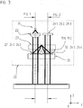
- FIGS. 1 and 2 show in each case in schematic form partial scanning beam paths in a lateral view in the xz plane, while FIG. 3 shows a view of the scanning beam in the yz plane.
- FIG. 1 the scanning beam path is shown from the light source 21 to the reflector elements 26.1 and 26.2
- FIG. 2 illustrates the scanning beam from the reflector elements 26.1 and 26.2 to the detector elements 29.1, 29.2, 29.3 of the optoelectronic detector array.
- the FIGS. 4 and 5 each show plan views of the scanning plate 25 and the reflector plate 23 with the optical elements provided there.
- the position-measuring device comprises a measuring scale 10 and a scanning unit 20 movable relative thereto in at least one measuring direction x.
- the objects whose relative position is to be determined by means of the position measuring device may be, for example, machine parts whose relative position must be precisely recorded; the scanning signals or position data generated by means of the position measuring device are further processed by a follow-up electronic or evaluation unit, for example, for controlling the machine, not shown.
- a position measuring device for detecting linear movements is shown with a linearly extending material measure;
- rotary position measuring devices based on the inventive considerations can be realized.
- That of light source 21, e.g. a laser diode, emitted, linearly polarized beams is first collimated in the illustrated example via a collimator lens 22, i. converted into a parallel beam. Subsequently, this beam passes through optically ineffective window areas 28.1, 27 of a reflector plate 23 and a scanning plate 25.
- the reflector plate 23 and the scanning 25 consist in this example of a plate-shaped, transparent support substrate, such as glass, on which a number of optical elements, such as Reflector elements 26.1, 26.2 and the grid structures 24.1 - 24.4, 32 are arranged.
- the concrete function of the various optical elements in the scanning beam path will be explained in detail below.
- the collimated beam then impinges for a first time on the material measure 10, which is formed in this example as a linear Auflichtdorfstab.
- the material measure 10 comprises a periodic arrangement of division regions with different directions extending in the measuring direction x optical properties.
- the measuring scale 10 is a reflection diffraction grating whose grating lines extend in the scale graduation plane in the indicated y-direction; In the following, inter alia, also the so-called line direction y will be mentioned.
- the first grating structures 24.1, 24.2 exert a defined optical lens effect on the penetrating partial beams. On the one hand, this is a defined deflection effect on the partial beams, whereby they are deflected antiparallel to the direction of incidence in measuring direction x.
- the first grating structures 24.1, 24.2 are designed as so-called offaxis cylindrical lenses on the scanning plate 25. Their focal lengths correspond to the optical distance to the reflector plate 23.
- Such a configuration of the optical properties of the first grating structures 24.1, 24.2 causes the main rays of the focused partial beams meet in the line direction y at a defined angle to the reflector plate 23 and thereby a spatial separation of the on the Reflector plate 23 incoming and outgoing partial beam results; this is about on the FIG. 3 directed.
- FIG. 4 A plan view of the scanning plate 25 with the first grid structures 24.1, 24.2 arranged thereon is shown in FIG. 4 shown. It can be seen here that these grating structures 24.1, 24.2 each have curved grating lines which are arranged equidistantly in the measuring direction x.
- the first grating structures 24.1, 24.2 are formed as phase gratings which suppress the 0th diffraction order; Particularly advantageous in this case are so-called blazed phase gratings which have a high efficiency in the +1. Diffraction order or in the -1. Have diffraction order.
- the thus deflected and focused partial beams then pass to the reflector elements 26.1, 26.2, which are arranged in the present example on the upper side of the reflector plate 23 and formed as a plane mirror reflectors.
- the scanning unit 20 Before the partial beams impinge a second time on the measuring scale 10, in the scanning unit 20 in the illustrated example, they first pass through in each case one polarization-optical element 31.1, 31.2 in the form of a single reflector element 26.1, 26.2 ⁇ / 4 plate and then second grating structures 24.3, 24.4, which are also arranged on the scanning plate 25. For this, turn to the illustration in FIG. 3 directed.
- the polarization-optical elements 31.1, 31.2 in each case oppositely circular-polarized partial beams are generated from the linear-polarized partial beams.
- the second grating structures 24.3, 24.4 also have a defined lens effect for the penetrating partial beams.
- the circularly polarized partial beam bundles experience a deflection effect in the measuring direction x and at least one collimating effect perpendicular to the measuring direction x, ie in the line direction y.
- the second grating structures 24.3, 24.4 of this example are designed as so-called offaxis lenses; Otherwise, with regard to the embodiment of the same, reference is made to the previous explanations of the first lattice structures 24.1, 24.2.
- the deflected by the second grating structures 24.3, 24.4 and at least in the y-direction (partially) collimated partial beams then pass a second time on the measuring scale 10, where a new diffraction and return reflection of the partial beams in the form of +/- 1st diffraction orders in Direction of the scanning unit 20 results.
- the partial beams reflected back vertically in the direction of the scanning unit 20 strike a splitting grating 32, which is arranged on the scanning plate 25, as a superposed, now again linearly polarized beam.
- the polarization direction of the radiation beam impinging on the splitting grating 32 depends on the relative position of the material measure 10 to the scanning unit 20.
- the material measure 10 is displaced by a quarter of its lattice constant in the measuring direction x, a phase shift of 360.degree. Between the partial beam bundles brought to the superposition takes place due to the two-time flexion at the measuring scale 10 into the +/- 1st diffraction orders.
- the polarization direction of the resulting linearly polarized beam changes by 180 °, which corresponds to a signal period in the resulting scanning signal.
- the splitting grating 32 of the present example has a dividing structure which is periodic in the measuring direction x and whose graduation lines extend in the y direction. As shown, the splitting grating 32 results in a splitting of the incident beam into three different spatial directions. Detector elements 29.1 - 29.3 of an optoelectronic detector arrangement are respectively placed in the different spatial directions, onto which the split radiation beams impinge on the reflector plate 23 after passing through optically ineffective window areas 28.2. At the detector elements 29.1 - 29.3 result in the case of the relative movement of measuring scale 10 and the scanning unit 20, the modulated shift dependent Sampling signals that can be further processed in a known manner.
- a further polarization-optical element 30.1 - 30.3 is arranged in the form of a polarizer in order to produce in this way three scanning signals shifted in phase by +/- 120 °.
- the reflector elements 26.1, 26.2 could in principle also be arranged on the underside of the reflector plate 23.
- Vernier or Moire sensing principles come into consideration, in which then the lattice constants of the material measure and the first and second lattice structures slightly different (Vernier system) or with slightly different angular orientation (moire system) choose. In the detection plane then results in a periodic fringe pattern, which is modulated shift-dependent and can be scanned in a known manner.
- all the polarization-optical components of the illustrated first embodiment i. the above-mentioned ⁇ / 4 plates 31.1, 31.2, the polarizers 30.1, 30.2, 30.3 and the splitter grid 32.
- a so-called structured detector arrangement would be placed in the detection plane, via which a scan of the strip pattern resulting therefrom and a conversion of the same takes place in phase-shifted scanning signals.
- optical components such as cylindrical lens arrays or grating structures could also be used in this embodiment in a known manner in conjunction with planar detectors for scanning the fringe pattern.
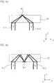
- FIG. 6a is a partial view of a corresponding device in the yz plane shown in the scanning beam, analogous to the previous representation of FIG. 3 ,
- a single transparent carrier substrate 40 is now provided, on the underside or of which the first and second grid structures 44.1, 44.2 are arranged - not shown - measuring scale facing side.
- the reflector element 46.1 is arranged, again formed as a simple plane mirror reflector.
- FIG. 6b shows a similar variant of a monolithic structure.
- a single transparent carrier substrate 50 is provided, in which the optically relevant elements in the form of the first and second grating structures 54.1, 54.2 and the reflector element 56.1 are now all arranged on the underside of the carrier substrate.
- the required deflection of the partial beams on the opposite upper side of the carrier substrate 50 can be effected for example via further reflector elements or reflective layers placed there.
- the light source does not necessarily have to be integrated in the scanning unit as described in the above example.
- the light source it is also possible to arrange the light source away from it and to supply the illumination beam to the scanning unit by means of light guides, etc.
- the partial beams to be detected are then supplied to the detector elements, for example via optical fibers.
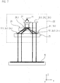
- FIGS. 7 to 9 Another variant of the first embodiment is in the FIGS. 7 to 9 shown schematically. Functionally equivalent elements of this embodiment are hereby denoted by the same reference numerals as in the example explained above. Below are just the differences described above to the example, otherwise reference is made to the previous statements.
- each deflecting 27.1, 28.3 to arrange.
- the deflecting gratings 27.1, 28.3 each have dividing lines, which are arranged periodically in the y-direction and extend in the measuring direction x.
- the periodicities of the two deflection gratings 27.1, 28.3 in the now optically effective window areas are selected identically.
- FIG. 10 - 12 A second embodiment of the position-measuring device according to the invention is described below with reference to FIG Figures 10 - 12 described.
- the basic structure of this embodiment of the position measuring device according to the invention and the course of the scanning beam path is substantially identical to the first example explained. In the following, therefore, only the relevant differences will be explained again.
- the first grating structures 124.1, 124.2 now have as a lens effect in addition to the optical functionality according to the first example of the Figures 1 - 5 an additional focusing effect on the continuous partial beam in the measuring direction x.
- the first grating structures are designed as correspondingly dimensioned offaxis lenses whose focal lengths correspond to the optical distance to the reflector plate 123.
- Such a design of the optical properties of the first grating structures 124.1, 124.2 causes the main beam of the focused partial beam in the measuring direction x perpendicular to the reflector plate 123 hits, in the stroke direction y, however, at a defined angle.
- This angle is chosen such that in turn results in a spatial separation of the incident on the reflector plate 123 and exiting partial beams in the y-direction.
- the partial beams again undergo an optical lensing effect as already explained in the above example, ie a lowering antiparallel to the direction of incidence as well as a collimation of the same.
- the first grating structures 124.1, 124.2 formed in this embodiment as Offaxis lenses focus the respective partial beams in both lateral directions x, y and thus correspond in their optical lens effect to conventional cylindrically symmetrical lenses.
- the Offaxis cylindrical lenses of the first example have only a lens effect in the form of a focusing effect in the y direction.
- the reflector plate 123 is arranged as parallel as possible to the material measure.
- the additional optical effect of the first grating structures results in an optical retroreflector functionality resulting from the interaction of the grating structures 124.1 - 124.4 and the reflector elements 126.1, 126.2 in the scanning beam path.
- the same optical effect can now be achieved by significantly simpler constructed diffractive elements.
- the scanning-side arrangement of first grid structures, a reflector plate and second grid structures can also be used to redirect the partial beam bundles coming from the transmitted-light material measure back to the transmitted-light measuring standard after their first passage through them.
- the corresponding scanning unit then has to be known Way to enclose the measuring standard in the Umgriff.
Landscapes
- Physics & Mathematics (AREA)
- General Physics & Mathematics (AREA)
- Optical Transform (AREA)
- Length Measuring Devices By Optical Means (AREA)
Applications Claiming Priority (1)
| Application Number | Priority Date | Filing Date | Title |
|---|---|---|---|
| DE102005029917A DE102005029917A1 (de) | 2005-06-28 | 2005-06-28 | Positionsmesseinrichtung |
Publications (3)
| Publication Number | Publication Date |
|---|---|
| EP1739395A2 EP1739395A2 (de) | 2007-01-03 |
| EP1739395A3 EP1739395A3 (de) | 2015-03-25 |
| EP1739395B1 true EP1739395B1 (de) | 2016-12-14 |
Family
ID=37110275
Family Applications (1)
| Application Number | Title | Priority Date | Filing Date |
|---|---|---|---|
| EP06012138.1A Active EP1739395B1 (de) | 2005-06-28 | 2006-06-13 | Positionsmesseinrichtung |
Country Status (6)
| Country | Link |
|---|---|
| US (1) | US7471397B2 (zh) |
| EP (1) | EP1739395B1 (zh) |
| JP (1) | JP5005969B2 (zh) |
| CN (1) | CN100554868C (zh) |
| DE (1) | DE102005029917A1 (zh) |
| ES (1) | ES2610804T3 (zh) |
Families Citing this family (32)
| Publication number | Priority date | Publication date | Assignee | Title |
|---|---|---|---|---|
| US7641856B2 (en) * | 2004-05-14 | 2010-01-05 | Honeywell International Inc. | Portable sample analyzer with removable cartridge |
| DE102005029917A1 (de) * | 2005-06-28 | 2007-01-04 | Dr. Johannes Heidenhain Gmbh | Positionsmesseinrichtung |
| DE102006042743A1 (de) | 2006-09-12 | 2008-03-27 | Dr. Johannes Heidenhain Gmbh | Positionsmesseinrichtung |
| DE102007023300A1 (de) * | 2007-05-16 | 2008-11-20 | Dr. Johannes Heidenhain Gmbh | Positionsmesseinrichtung und Anordnung derselben |
| DE102008008873A1 (de) * | 2007-05-16 | 2008-11-20 | Dr. Johannes Heidenhain Gmbh | Positionsmesseinrichtung |
| DE102008007319A1 (de) | 2008-02-02 | 2009-08-06 | Dr. Johannes Heidenhain Gmbh | Optische Positionsmesseinrichtung |
| US7864336B2 (en) * | 2008-04-28 | 2011-01-04 | Agilent Technologies, Inc. | Compact Littrow encoder |
| KR20110086025A (ko) * | 2008-10-23 | 2011-07-27 | 가부시키가이샤 니콘 | 인코더 |
| KR101725529B1 (ko) | 2010-03-30 | 2017-04-10 | 지고 코포레이션 | 간섭계 인코더 시스템 |
| DE102010029211A1 (de) | 2010-05-21 | 2011-11-24 | Dr. Johannes Heidenhain Gmbh | Optische Positionsmesseinrichtung |
| NL2006743A (en) * | 2010-06-09 | 2011-12-12 | Asml Netherlands Bv | Position sensor and lithographic apparatus. |
| DE102011081879A1 (de) * | 2010-11-03 | 2012-05-03 | Dr. Johannes Heidenhain Gmbh | Optische Winkelmesseinrichtung |
| DE102010043469A1 (de) * | 2010-11-05 | 2012-05-10 | Dr. Johannes Heidenhain Gmbh | Optische Positionsmesseinrichtung |
| DE102011082156A1 (de) * | 2010-12-16 | 2012-06-21 | Dr. Johannes Heidenhain Gmbh | Optische Positionsmesseinrichtung |
| JP5849103B2 (ja) | 2011-02-01 | 2016-01-27 | ザイゴ コーポレーションZygo Corporation | 干渉ヘテロダイン光学エンコーダシステム |
| DE102011005937B4 (de) * | 2011-03-23 | 2020-10-22 | Dr. Johannes Heidenhain Gmbh | Vorrichtung zur interferentiellen Abstandsmessung |
| DE102011076178B4 (de) | 2011-05-20 | 2022-03-31 | Dr. Johannes Heidenhain Gmbh | Positionsmesseinrichtung |
| US9534934B2 (en) * | 2011-09-06 | 2017-01-03 | Nikon Corporation | High resolution encoder head |
| WO2013070957A1 (en) | 2011-11-09 | 2013-05-16 | Zygo Corporation | Compact encoder head for interferometric encoder system |
| KR101521146B1 (ko) | 2011-11-09 | 2015-05-18 | 지고 코포레이션 | 이중 패스 간섭측정식 인코더 시스템 |
| DE102012204572A1 (de) * | 2012-03-22 | 2013-09-26 | Dr. Johannes Heidenhain Gmbh | Positionsmesseinrichtung und Anordnung mit einer derartigen Positionsmesseinrichtung |
| TWI516746B (zh) | 2012-04-20 | 2016-01-11 | 賽格股份有限公司 | 在干涉編碼系統中執行非諧循環錯誤補償的方法、裝置及計算機程式產品,以及微影系統 |
| DE102012210309A1 (de) * | 2012-06-19 | 2013-12-19 | Dr. Johannes Heidenhain Gmbh | Positionsmesseinrichtung |
| DE102013222383A1 (de) * | 2013-02-06 | 2014-08-07 | Dr. Johannes Heidenhain Gmbh | Optische Positionsmesseinrichtung |
| DE102013211758A1 (de) * | 2013-06-21 | 2014-12-24 | Dr. Johannes Heidenhain Gmbh | Interferometer |
| TWI627379B (zh) | 2013-10-07 | 2018-06-21 | 德商強那斯海登翰博士有限公司 | 光學位置測量裝置 |
| DE102013220190B4 (de) * | 2013-10-07 | 2021-08-12 | Dr. Johannes Heidenhain Gmbh | Messteilung und lichtelektrische Positionsmesseinrichtung mit dieser Messteilung |
| JP6593868B2 (ja) * | 2015-07-28 | 2019-10-23 | 株式会社ミツトヨ | 変位検出装置 |
| CN106813578B (zh) * | 2015-11-30 | 2019-02-22 | 上海微电子装备(集团)股份有限公司 | 一种二维光栅测量系统 |
| DE102016200847A1 (de) * | 2016-01-21 | 2017-07-27 | Dr. Johannes Heidenhain Gesellschaft Mit Beschränkter Haftung | Optische Positionsmesseinrichtung |
| JP2018066629A (ja) * | 2016-10-19 | 2018-04-26 | 太陽誘電株式会社 | ロードセル |
| US10648838B2 (en) | 2017-06-29 | 2020-05-12 | Mitutoyo Corporation | Contamination and defect resistant rotary optical encoder configuration including a rotary scale with yawed scale grating bars and structured illumination generating arrangement with a beam deflector configuration |
Family Cites Families (13)
| Publication number | Priority date | Publication date | Assignee | Title |
|---|---|---|---|---|
| DE3872227T2 (de) * | 1987-12-15 | 1992-12-03 | Renishaw Plc | Opto-elektronischer skalenlese-apparat. |
| DE3905730C2 (de) * | 1989-02-24 | 1995-06-14 | Heidenhain Gmbh Dr Johannes | Positionsmeßeinrichtung |
| US5079418A (en) | 1990-02-20 | 1992-01-07 | Dr. Johannes Heidenhain Gmbh | Position measuring apparatus with reflection |
| JP3478567B2 (ja) * | 1992-09-25 | 2003-12-15 | キヤノン株式会社 | 回転情報検出装置 |
| JP3028716B2 (ja) * | 1993-09-29 | 2000-04-04 | キヤノン株式会社 | 光学式変位センサ |
| JP3530573B2 (ja) * | 1994-04-27 | 2004-05-24 | キヤノン株式会社 | 光学式変位センサ |
| DE19748802B4 (de) * | 1996-11-20 | 2010-09-09 | Dr. Johannes Heidenhain Gmbh | Optische Positionsmeßeinrichtung |
| CN1248058C (zh) * | 2000-09-14 | 2006-03-29 | 约翰尼斯海登海恩博士股份有限公司 | 位置测量装置 |
| US20030174343A1 (en) * | 2002-03-18 | 2003-09-18 | Mitutoyo Corporation | Optical displacement sensing device with reduced sensitivity to misalignment |
| EP1347271B1 (en) | 2002-03-18 | 2012-01-11 | Mitutoyo Corporation | Optical displacement sensing device with reduced sensitivity to misalignment |
| JP4722474B2 (ja) * | 2004-12-24 | 2011-07-13 | 株式会社ミツトヨ | 変位検出装置 |
| DE102005029917A1 (de) * | 2005-06-28 | 2007-01-04 | Dr. Johannes Heidenhain Gmbh | Positionsmesseinrichtung |
| JP5147368B2 (ja) * | 2006-11-20 | 2013-02-20 | ドクトル・ヨハネス・ハイデンハイン・ゲゼルシヤフト・ミツト・ベシユレンクテル・ハフツング | エンコーダ |
-
2005
- 2005-06-28 DE DE102005029917A patent/DE102005029917A1/de not_active Withdrawn
-
2006
- 2006-06-13 EP EP06012138.1A patent/EP1739395B1/de active Active
- 2006-06-13 ES ES06012138.1T patent/ES2610804T3/es active Active
- 2006-06-27 JP JP2006176321A patent/JP5005969B2/ja active Active
- 2006-06-28 CN CNB2006100996840A patent/CN100554868C/zh active Active
- 2006-06-28 US US11/478,168 patent/US7471397B2/en active Active
Non-Patent Citations (1)
| Title |
|---|
| None * |
Also Published As
| Publication number | Publication date |
|---|---|
| EP1739395A3 (de) | 2015-03-25 |
| DE102005029917A1 (de) | 2007-01-04 |
| JP2007010659A (ja) | 2007-01-18 |
| CN100554868C (zh) | 2009-10-28 |
| EP1739395A2 (de) | 2007-01-03 |
| US7471397B2 (en) | 2008-12-30 |
| ES2610804T3 (es) | 2017-05-03 |
| US20070013920A1 (en) | 2007-01-18 |
| CN1892173A (zh) | 2007-01-10 |
| JP5005969B2 (ja) | 2012-08-22 |
Similar Documents
| Publication | Publication Date | Title |
|---|---|---|
| EP1739395B1 (de) | Positionsmesseinrichtung | |
| EP1901041B1 (de) | Positionsmesseinrichtung | |
| EP1319170B1 (de) | Positionsmesseinrichtung | |
| EP2085752B1 (de) | Optische Positionsmesseinrichtung | |
| EP2149036B1 (de) | Optische positionsmesseinrichtung | |
| EP1396704B1 (de) | Interferenzielle Positionsmesseinrichtung | |
| EP2474815B1 (de) | Optische Positionsmesseinrichtung | |
| EP0735346B1 (de) | Lichtelektrische Positionsmesseinrichtung | |
| DE19748802B4 (de) | Optische Positionsmeßeinrichtung | |
| EP2848899B1 (de) | Optische Positionsmesseinrichtung | |
| DE102010003157A1 (de) | Vorrichtung zur interferentiellen Abstandsmessung | |
| DE19930687B4 (de) | Optisches Verschiebungsmeßsystem | |
| EP2565578B1 (de) | Vorrichtung zur interferometrischen Abstandsbestimmung zwischen zwei parallelen Platten | |
| DE102015218539A1 (de) | Optische Positionsmesseinrichtung | |
| EP3059554B1 (de) | Optische positionsmesseinrichtung | |
| DE19938869B4 (de) | Optisches Verschiebungsmeßsystem | |
| DE102011076178A1 (de) | Positionsmesseinrichtung | |
| EP3477264B1 (de) | Optische positionsmesseinrichtung | |
| EP0747674B1 (de) | Lichtelektrische Positionsmesseinrichtung | |
| DE102011005937B4 (de) | Vorrichtung zur interferentiellen Abstandsmessung | |
| EP3045873B1 (de) | Optische positionsmesseinrichtung | |
| WO2014170066A1 (de) | Vorrichtung zur interferentiellen abstandsmessung | |
| EP3936830B1 (de) | Optische positionsmesseinrichtung | |
| EP2356405B1 (de) | Optische positionsmesseinrichtung |
Legal Events
| Date | Code | Title | Description |
|---|---|---|---|
| PUAI | Public reference made under article 153(3) epc to a published international application that has entered the european phase |
Free format text: ORIGINAL CODE: 0009012 |
|
| AK | Designated contracting states |
Kind code of ref document: A2 Designated state(s): AT BE BG CH CY CZ DE DK EE ES FI FR GB GR HU IE IS IT LI LT LU LV MC NL PL PT RO SE SI SK TR |
|
| AX | Request for extension of the european patent |
Extension state: AL BA HR MK YU |
|
| PUAL | Search report despatched |
Free format text: ORIGINAL CODE: 0009013 |
|
| AK | Designated contracting states |
Kind code of ref document: A3 Designated state(s): AT BE BG CH CY CZ DE DK EE ES FI FR GB GR HU IE IS IT LI LT LU LV MC NL PL PT RO SE SI SK TR |
|
| AX | Request for extension of the european patent |
Extension state: AL BA HR MK RS |
|
| RIC1 | Information provided on ipc code assigned before grant |
Ipc: G01D 5/347 20060101ALI20150219BHEP Ipc: G01D 5/38 20060101AFI20150219BHEP |
|
| 17P | Request for examination filed |
Effective date: 20150409 |
|
| RBV | Designated contracting states (corrected) |
Designated state(s): AT BE BG CH CY CZ DE DK EE ES FI FR GB GR HU IE IS IT LI LT LU LV MC NL PL PT RO SE SI SK TR |
|
| AKX | Designation fees paid |
Designated state(s): AT BE BG CH CY CZ DE DK EE ES FI FR GB GR HU IE IS IT LI LT LU LV MC NL PL PT RO SE SI SK TR |
|
| AXX | Extension fees paid |
Extension state: MK Extension state: HR Extension state: RS Extension state: AL Extension state: BA |
|
| GRAP | Despatch of communication of intention to grant a patent |
Free format text: ORIGINAL CODE: EPIDOSNIGR1 |
|
| INTG | Intention to grant announced |
Effective date: 20160920 |
|
| GRAS | Grant fee paid |
Free format text: ORIGINAL CODE: EPIDOSNIGR3 |
|
| GRAA | (expected) grant |
Free format text: ORIGINAL CODE: 0009210 |
|
| AK | Designated contracting states |
Kind code of ref document: B1 Designated state(s): AT BE BG CH CY CZ DE DK EE ES FI FR GB GR HU IE IS IT LI LT LU LV MC NL PL PT RO SE SI SK TR |
|
| REG | Reference to a national code |
Ref country code: GB Ref legal event code: FG4D Free format text: NOT ENGLISH |
|
| REG | Reference to a national code |
Ref country code: CH Ref legal event code: EP Ref country code: CH Ref legal event code: NV Representative=s name: ICB INGENIEURS CONSEILS EN BREVETS SA, CH |
|
| REG | Reference to a national code |
Ref country code: IE Ref legal event code: FG4D Free format text: LANGUAGE OF EP DOCUMENT: GERMAN |
|
| REG | Reference to a national code |
Ref country code: AT Ref legal event code: REF Ref document number: 854007 Country of ref document: AT Kind code of ref document: T Effective date: 20170115 |
|
| REG | Reference to a national code |
Ref country code: DE Ref legal event code: R096 Ref document number: 502006015287 Country of ref document: DE |
|
| REG | Reference to a national code |
Ref country code: NL Ref legal event code: FP |
|
| PG25 | Lapsed in a contracting state [announced via postgrant information from national office to epo] |
Ref country code: LV Free format text: LAPSE BECAUSE OF FAILURE TO SUBMIT A TRANSLATION OF THE DESCRIPTION OR TO PAY THE FEE WITHIN THE PRESCRIBED TIME-LIMIT Effective date: 20161214 |
|
| REG | Reference to a national code |
Ref country code: LT Ref legal event code: MG4D |
|
| PG25 | Lapsed in a contracting state [announced via postgrant information from national office to epo] |
Ref country code: SE Free format text: LAPSE BECAUSE OF FAILURE TO SUBMIT A TRANSLATION OF THE DESCRIPTION OR TO PAY THE FEE WITHIN THE PRESCRIBED TIME-LIMIT Effective date: 20161214 Ref country code: LT Free format text: LAPSE BECAUSE OF FAILURE TO SUBMIT A TRANSLATION OF THE DESCRIPTION OR TO PAY THE FEE WITHIN THE PRESCRIBED TIME-LIMIT Effective date: 20161214 Ref country code: GR Free format text: LAPSE BECAUSE OF FAILURE TO SUBMIT A TRANSLATION OF THE DESCRIPTION OR TO PAY THE FEE WITHIN THE PRESCRIBED TIME-LIMIT Effective date: 20170315 |
|
| REG | Reference to a national code |
Ref country code: ES Ref legal event code: FG2A Ref document number: 2610804 Country of ref document: ES Kind code of ref document: T3 Effective date: 20170503 |
|
| PG25 | Lapsed in a contracting state [announced via postgrant information from national office to epo] |
Ref country code: FI Free format text: LAPSE BECAUSE OF FAILURE TO SUBMIT A TRANSLATION OF THE DESCRIPTION OR TO PAY THE FEE WITHIN THE PRESCRIBED TIME-LIMIT Effective date: 20161214 |
|
| PG25 | Lapsed in a contracting state [announced via postgrant information from national office to epo] |
Ref country code: SK Free format text: LAPSE BECAUSE OF FAILURE TO SUBMIT A TRANSLATION OF THE DESCRIPTION OR TO PAY THE FEE WITHIN THE PRESCRIBED TIME-LIMIT Effective date: 20161214 Ref country code: IS Free format text: LAPSE BECAUSE OF FAILURE TO SUBMIT A TRANSLATION OF THE DESCRIPTION OR TO PAY THE FEE WITHIN THE PRESCRIBED TIME-LIMIT Effective date: 20170414 Ref country code: CZ Free format text: LAPSE BECAUSE OF FAILURE TO SUBMIT A TRANSLATION OF THE DESCRIPTION OR TO PAY THE FEE WITHIN THE PRESCRIBED TIME-LIMIT Effective date: 20161214 Ref country code: RO Free format text: LAPSE BECAUSE OF FAILURE TO SUBMIT A TRANSLATION OF THE DESCRIPTION OR TO PAY THE FEE WITHIN THE PRESCRIBED TIME-LIMIT Effective date: 20161214 Ref country code: EE Free format text: LAPSE BECAUSE OF FAILURE TO SUBMIT A TRANSLATION OF THE DESCRIPTION OR TO PAY THE FEE WITHIN THE PRESCRIBED TIME-LIMIT Effective date: 20161214 |
|
| PG25 | Lapsed in a contracting state [announced via postgrant information from national office to epo] |
Ref country code: PT Free format text: LAPSE BECAUSE OF FAILURE TO SUBMIT A TRANSLATION OF THE DESCRIPTION OR TO PAY THE FEE WITHIN THE PRESCRIBED TIME-LIMIT Effective date: 20170414 Ref country code: BG Free format text: LAPSE BECAUSE OF FAILURE TO SUBMIT A TRANSLATION OF THE DESCRIPTION OR TO PAY THE FEE WITHIN THE PRESCRIBED TIME-LIMIT Effective date: 20170314 Ref country code: IT Free format text: LAPSE BECAUSE OF FAILURE TO SUBMIT A TRANSLATION OF THE DESCRIPTION OR TO PAY THE FEE WITHIN THE PRESCRIBED TIME-LIMIT Effective date: 20161214 Ref country code: PL Free format text: LAPSE BECAUSE OF FAILURE TO SUBMIT A TRANSLATION OF THE DESCRIPTION OR TO PAY THE FEE WITHIN THE PRESCRIBED TIME-LIMIT Effective date: 20161214 |
|
| REG | Reference to a national code |
Ref country code: DE Ref legal event code: R097 Ref document number: 502006015287 Country of ref document: DE |
|
| PLBE | No opposition filed within time limit |
Free format text: ORIGINAL CODE: 0009261 |
|
| STAA | Information on the status of an ep patent application or granted ep patent |
Free format text: STATUS: NO OPPOSITION FILED WITHIN TIME LIMIT |
|
| 26N | No opposition filed |
Effective date: 20170915 |
|
| PG25 | Lapsed in a contracting state [announced via postgrant information from national office to epo] |
Ref country code: DK Free format text: LAPSE BECAUSE OF FAILURE TO SUBMIT A TRANSLATION OF THE DESCRIPTION OR TO PAY THE FEE WITHIN THE PRESCRIBED TIME-LIMIT Effective date: 20161214 |
|
| PG25 | Lapsed in a contracting state [announced via postgrant information from national office to epo] |
Ref country code: MC Free format text: LAPSE BECAUSE OF FAILURE TO SUBMIT A TRANSLATION OF THE DESCRIPTION OR TO PAY THE FEE WITHIN THE PRESCRIBED TIME-LIMIT Effective date: 20161214 |
|
| PG25 | Lapsed in a contracting state [announced via postgrant information from national office to epo] |
Ref country code: SI Free format text: LAPSE BECAUSE OF FAILURE TO SUBMIT A TRANSLATION OF THE DESCRIPTION OR TO PAY THE FEE WITHIN THE PRESCRIBED TIME-LIMIT Effective date: 20161214 |
|
| REG | Reference to a national code |
Ref country code: IE Ref legal event code: MM4A |
|
| REG | Reference to a national code |
Ref country code: FR Ref legal event code: ST Effective date: 20180228 |
|
| PG25 | Lapsed in a contracting state [announced via postgrant information from national office to epo] |
Ref country code: LU Free format text: LAPSE BECAUSE OF NON-PAYMENT OF DUE FEES Effective date: 20170613 Ref country code: IE Free format text: LAPSE BECAUSE OF NON-PAYMENT OF DUE FEES Effective date: 20170613 |
|
| PG25 | Lapsed in a contracting state [announced via postgrant information from national office to epo] |
Ref country code: FR Free format text: LAPSE BECAUSE OF NON-PAYMENT OF DUE FEES Effective date: 20170630 |
|
| REG | Reference to a national code |
Ref country code: BE Ref legal event code: MM Effective date: 20170630 |
|
| REG | Reference to a national code |
Ref country code: AT Ref legal event code: MM01 Ref document number: 854007 Country of ref document: AT Kind code of ref document: T Effective date: 20170613 |
|
| PG25 | Lapsed in a contracting state [announced via postgrant information from national office to epo] |
Ref country code: BE Free format text: LAPSE BECAUSE OF NON-PAYMENT OF DUE FEES Effective date: 20170630 |
|
| PG25 | Lapsed in a contracting state [announced via postgrant information from national office to epo] |
Ref country code: AT Free format text: LAPSE BECAUSE OF NON-PAYMENT OF DUE FEES Effective date: 20170613 |
|
| PG25 | Lapsed in a contracting state [announced via postgrant information from national office to epo] |
Ref country code: HU Free format text: LAPSE BECAUSE OF FAILURE TO SUBMIT A TRANSLATION OF THE DESCRIPTION OR TO PAY THE FEE WITHIN THE PRESCRIBED TIME-LIMIT; INVALID AB INITIO Effective date: 20060613 |
|
| PG25 | Lapsed in a contracting state [announced via postgrant information from national office to epo] |
Ref country code: CY Free format text: LAPSE BECAUSE OF NON-PAYMENT OF DUE FEES Effective date: 20161214 |
|
| PG25 | Lapsed in a contracting state [announced via postgrant information from national office to epo] |
Ref country code: TR Free format text: LAPSE BECAUSE OF FAILURE TO SUBMIT A TRANSLATION OF THE DESCRIPTION OR TO PAY THE FEE WITHIN THE PRESCRIBED TIME-LIMIT Effective date: 20161214 |
|
| PGFP | Annual fee paid to national office [announced via postgrant information from national office to epo] |
Ref country code: CH Payment date: 20220701 Year of fee payment: 17 |
|
| PGFP | Annual fee paid to national office [announced via postgrant information from national office to epo] |
Ref country code: NL Payment date: 20230620 Year of fee payment: 18 Ref country code: DE Payment date: 20230620 Year of fee payment: 18 |
|
| PGFP | Annual fee paid to national office [announced via postgrant information from national office to epo] |
Ref country code: GB Payment date: 20230620 Year of fee payment: 18 Ref country code: ES Payment date: 20230828 Year of fee payment: 18 |
|
| REG | Reference to a national code |
Ref country code: CH Ref legal event code: PL |
|
| PG25 | Lapsed in a contracting state [announced via postgrant information from national office to epo] |
Ref country code: CH Free format text: LAPSE BECAUSE OF NON-PAYMENT OF DUE FEES Effective date: 20230630 |