EP1737112A2 - Verfahren und Vorrichtung zur Steuerung der Ausgangsleistung eines Schaltnetzteils - Google Patents
Verfahren und Vorrichtung zur Steuerung der Ausgangsleistung eines Schaltnetzteils Download PDFInfo
- Publication number
- EP1737112A2 EP1737112A2 EP05257869A EP05257869A EP1737112A2 EP 1737112 A2 EP1737112 A2 EP 1737112A2 EP 05257869 A EP05257869 A EP 05257869A EP 05257869 A EP05257869 A EP 05257869A EP 1737112 A2 EP1737112 A2 EP 1737112A2
- Authority
- EP
- European Patent Office
- Prior art keywords
- output
- power supply
- unregulated
- region
- threshold
- Prior art date
- Legal status (The legal status is an assumption and is not a legal conclusion. Google has not performed a legal analysis and makes no representation as to the accuracy of the status listed.)
- Withdrawn
Links
Images


Classifications
-
- H—ELECTRICITY
- H02—GENERATION; CONVERSION OR DISTRIBUTION OF ELECTRIC POWER
- H02M—APPARATUS FOR CONVERSION BETWEEN AC AND AC, BETWEEN AC AND DC, OR BETWEEN DC AND DC, AND FOR USE WITH MAINS OR SIMILAR POWER SUPPLY SYSTEMS; CONVERSION OF DC OR AC INPUT POWER INTO SURGE OUTPUT POWER; CONTROL OR REGULATION THEREOF
- H02M1/00—Details of apparatus for conversion
- H02M1/32—Means for protecting converters other than automatic disconnection
-
- H—ELECTRICITY
- H02—GENERATION; CONVERSION OR DISTRIBUTION OF ELECTRIC POWER
- H02M—APPARATUS FOR CONVERSION BETWEEN AC AND AC, BETWEEN AC AND DC, OR BETWEEN DC AND DC, AND FOR USE WITH MAINS OR SIMILAR POWER SUPPLY SYSTEMS; CONVERSION OF DC OR AC INPUT POWER INTO SURGE OUTPUT POWER; CONTROL OR REGULATION THEREOF
- H02M3/00—Conversion of DC power input into DC power output
- H02M3/02—Conversion of DC power input into DC power output without intermediate conversion into AC
- H02M3/04—Conversion of DC power input into DC power output without intermediate conversion into AC by static converters
- H02M3/10—Conversion of DC power input into DC power output without intermediate conversion into AC by static converters using discharge tubes with control electrode or semiconductor devices with control electrode
- H02M3/145—Conversion of DC power input into DC power output without intermediate conversion into AC by static converters using discharge tubes with control electrode or semiconductor devices with control electrode using devices of a triode or transistor type requiring continuous application of a control signal
- H02M3/155—Conversion of DC power input into DC power output without intermediate conversion into AC by static converters using discharge tubes with control electrode or semiconductor devices with control electrode using devices of a triode or transistor type requiring continuous application of a control signal using semiconductor devices only
- H02M3/156—Conversion of DC power input into DC power output without intermediate conversion into AC by static converters using discharge tubes with control electrode or semiconductor devices with control electrode using devices of a triode or transistor type requiring continuous application of a control signal using semiconductor devices only with automatic control of output voltage or current, e.g. switching regulators
-
- H—ELECTRICITY
- H02—GENERATION; CONVERSION OR DISTRIBUTION OF ELECTRIC POWER
- H02M—APPARATUS FOR CONVERSION BETWEEN AC AND AC, BETWEEN AC AND DC, OR BETWEEN DC AND DC, AND FOR USE WITH MAINS OR SIMILAR POWER SUPPLY SYSTEMS; CONVERSION OF DC OR AC INPUT POWER INTO SURGE OUTPUT POWER; CONTROL OR REGULATION THEREOF
- H02M3/00—Conversion of DC power input into DC power output
- H02M3/22—Conversion of DC power input into DC power output with intermediate conversion into AC
- H02M3/24—Conversion of DC power input into DC power output with intermediate conversion into AC by static converters
- H02M3/28—Conversion of DC power input into DC power output with intermediate conversion into AC by static converters using discharge tubes with control electrode or semiconductor devices with control electrode to produce the intermediate AC
- H02M3/325—Conversion of DC power input into DC power output with intermediate conversion into AC by static converters using discharge tubes with control electrode or semiconductor devices with control electrode to produce the intermediate AC using devices of a triode or a transistor type requiring continuous application of a control signal
- H02M3/335—Conversion of DC power input into DC power output with intermediate conversion into AC by static converters using discharge tubes with control electrode or semiconductor devices with control electrode to produce the intermediate AC using devices of a triode or a transistor type requiring continuous application of a control signal using semiconductor devices only
- H02M3/33507—Conversion of DC power input into DC power output with intermediate conversion into AC by static converters using discharge tubes with control electrode or semiconductor devices with control electrode to produce the intermediate AC using devices of a triode or a transistor type requiring continuous application of a control signal using semiconductor devices only with automatic control of the output voltage or current, e.g. flyback converters
Definitions
- the present invention relates generally to electronic circuits, and more specifically, the invention relates to switching power supplies.
- a common application of switching power supplies is to charge batteries.
- the output power of a battery charger is usually controlled to provide a regulated voltage and a regulated current.
- the voltage is regulated between a maximum and a minimum voltage over a range of output current.
- the current is regulated between a maximum and a minimum current over a range of output voltage.
- As the battery charges there is usually an abrupt transition from regulated output current to regulated output voltage that occurs automatically when the battery voltage reaches a threshold. That is, the locus of output voltage and output current plotted in Cartesian coordinates usually has a sharp corner at the point of transition that corresponds to the point of maximum output power.
- the practice of designing a battery charger to have a sharp transition between regulated voltage and regulated current can result in a product that costs more than necessary to provide the desired function. It is often possible to reduce the cost of the battery charger and to meet all requirements by designing an unregulated transition between the regulated voltage and the regulated current.
- the output voltage and output current in the region of unregulated transition is bounded by the natural output characteristics of the switching regulator, and typically follows the curve of maximum output power for a given output voltage or current.
- the switching regulator is designed to operate with a control circuit that permits the regulator to make an unregulated transition between regulated output voltage and regulated output current such that the voltage and current are maintained within the specified boundaries.
- Proper design of the unregulated transition within the specified boundaries reduces the maximum power output, allowing the use of components that are less costly than the components to guarantee higher output power.
- the control circuit operates the switching regulator for regulated voltage, regulated current, unregulated transition, or self-protection according to the magnitude of a feedback signal.
- a switching regulator comprising:
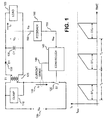
- Figure 1 is a functional block diagram of one embodiment of a switching regulator that may control output power in accordance with the teaching of the present invention.
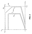
- Figure 2 is a diagram that shows the boundaries of output voltage and output current of one embodiment of a switching regulator that controls output power in accordance with the teachings of the present invention.
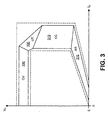
- Figure 3 shows four specific regions of operation within the boundaries of output voltage and output current for one embodiment of a switching regulator that controls output power in accordance with the teachings of the present invention.
- Figure 4 illustrates three specific regions of operation within the boundaries of output voltage and output current for another embodiment of a switching regulator that controls output power in accordance with the teachings of the present invention.
- Figure 5 is a flowchart of one embodiment of a method to control output power for an embodiment of a switching regulator in accordance with the teachings of the present invention.
- Figure 6 describes the control characteristics of one embodiment of a switching regulator that uses pulse width modulation to regulate an output in accordance with the teachings of the present invention.
- Figure 7 describes the control characteristics of one embodiment of a switching regulator that uses an on/off control to regulate an output in accordance with the teachings of the present invention.
- Figure 8 shows the output voltage and current characteristics of a typical switching regulator battery charger controlled in accordance with the teachings of the present invention.
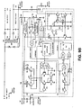
- Figure 9A is one embodiment of a circuit diagram of power supply with an integrated circuit controller in accordance with the teachings of the present invention.
- Figure 9B is another embodiment of a circuit diagram of power supply with an integrated circuit controller in accordance with the teachings of the present invention.
- Embodiments of a power supply regulator that may be utilized in a power supply are disclosed.
- numerous specific details are set forth in order to provide a thorough understanding of the present invention. It will be apparent, however, to one having ordinary skill in the art that the specific detail need not be employed to practice the present invention. Well-known methods related to the implementation have not been described in detail in order to avoid obscuring the present invention.
- Figure 1 shows a functional block diagram of a power supply that may include an embodiment of a power supply regulator that is a battery charger in accordance with the teachings of the present invention.
- the topology of the power supply illustrated in Figure 1 is known as a flyback regulator. It is appreciated that there are many topologies and configurations of switching regulators, and that the flyback topology shown in Figure 1 is provided to illustrate the principles of an embodiment of the present invention that may apply also to other types of topologies in accordance with the teachings of the present invention.
- the power supply in Figure 1 provides output power to a load 165 from an unregulated input voltage V IN 105.
- the load 165 may be a rechargeable battery.
- the input voltage V IN 105 is coupled to an energy transfer element T1 125 and a switch S1 120.
- the energy transfer element T1 125 is coupled between an input of the power supply and an output of the power supply.
- the energy transfer element T1 125 is illustrated as a transformer with two windings. In general, the transformer can have more than two windings, with additional windings to provide power to additional loads, to provide bias voltages, or to sense the voltage at a load.
- a clamp circuit 110 is coupled to the primary winding of the energy transfer element T1 125 to control the maximum voltage on the switch S1 120.
- Switch S1 120 is switched on and off in response to one embodiment of a controller circuit 145 in accordance with the teachings of the present invention.
- switch S 1 120 is a transistor such as for example a power metal oxide semiconductor field effect transistor (MOSFET).
- controller 145 includes integrated circuits and discrete electrical components. The operation of switch S1 120 produces pulsating current in the rectifier D1 130 that is filtered by capacitor C1 135 to produce a substantially constant output voltage V O or output current I O at the load 165.
- the output quantity to be regulated is U O 150, that in general could be an output voltage V O , an output current I O , or a combination of the two.
- the regulated quantity is not necessarily constant, but can be regulated to change in a desired way in response to a feedback signal. An output that does not respond to a feedback signal is unregulated.
- a feedback circuit 160 is coupled to the output quantity U O 150 to produce a feedback signal U FB 155 that is an input to the controller 145.
- Another input to the controller 145 is the current sense signal 140 that senses a current I D 115 in switch S 1 120.
- FIG. 1 also illustrates an example waveform for current I D 115 to show the parameters that the controller can adjust to regulate the output quantity U O 150.
- the maximum of current I D 115 is I MAX
- the switching period is T S
- the duty ratio is D.
- the controller typically limits the duty ratio to a maximum D MAX that is less than 100%.
- the controller 145 operates switch S 1 120 to substantially regulate the output Uo 150 to its desired value.
- the output U O changes from an output voltage to an output current in response to the magnitude of the output voltage or the output current.
- controller 145 includes an oscillator that defines substantially regular switching period T S .
- regulation is accomplished by control of the conduction time of the switch within a switching period. In each switching period, the fraction of the switching period that the switch is closed is the duty ratio D of the switch.
- regulation is accomplished by control of the maximum current I MAX of the switch. In another embodiment, regulation is accomplished by control of the switching period T S .
- the parameters of the regulator are substantially independent of the feedback signal U FB over a range of values of U FB .
- parameters I MAX , D, and T S can be either fixed or allowed to vary in response to changes in other quantities such as for example the input voltage V IN 105 or the load 165.
- changes are determined by the natural characteristics of the topology of the power converter, such as the flyback topology.
- a regulator can be designed so that an output behaves in a desired way when it is unregulated by a feedback signal in accordance with the teachings of the present invention.
- Figure 2 shows boundaries for output voltage and output current of one embodiment of a switching power supply that operates in accordance with the teachings of the present invention.
- the output of the power supply falls within the outer boundary 205 and the inner boundary 210.
- the outer boundary sets a maximum output voltage V OMAX and a maximum output current I OMAX that define a maximum output power P MAX at the intersection 200 of the lines for V OMAX and I OMAX .
- a power supply that has output characteristics within the region of the solid lines 215 will operate between the outer boundary 205 and the inner boundary 210 at less than the maximum output power P MAX .
- Such a power supply will typically cost less than one capable of operation at P MAX .
- FIG. 3 shows four specific regions within the boundaries of output voltage and output current for one embodiment of a power supply that operates in accordance with the teachings of the present invention.
- the CV region 300 is a region of regulated voltage where the variation in output voltage is restricted over a wide range of output current.
- the CC region 310 is a region of regulated current where the variation in output current is restricted over a wide range of output voltage.
- the UT region 305 is a transition region where the output voltage and the output current are unregulated between the CV region 300 and the CC region 310.
- the AR region 315 is an auto-restart region where the power supply operates at a reduced output voltage and reduced average output current to avoid damage from a short circuit fault on the output or from a fault that prevents the feedback signal from reaching the controller.
- the power supply operates in an auto-restart cycle.
- the controller allows the power switch to operate unregulated for a duration that is long enough to raise the output of the power supply above an auto-restart threshold when the load is within specifications, followed by a long interval of no switching if the output does not reach the threshold during the allowed duration of the switching.
- the auto-restart cycle repeats until the output of the power supply rises above the auto-restart threshold. It will be understood that not all applications will require an auto-restart region of operation. Some applications of embodiments of the present invention benefit from the UT region 315 without the AR region 315.
- Figure 4 illustrates how one embodiment of a power supply may operate within the specified boundaries of output voltage and output current with only one regulated region, constant voltage CV region 400.
- An unregulated transition UT region 405 is between a regulated constant voltage CV region 400 and an auto-restart AR region 415.
- requirements may be satisfied with only a constant voltage CV region 400 and an unregulated transition region UT region 405.
- the auto-restart AR region is not required, and the UT region 405 is extended to zero output voltage without substantial reduction in output current
- FIG. 5 is a flowchart illustration that describes one embodiment of a method to control the output power of a switching regulator in accordance with the teachings of the present invention.
- a feedback signal U FB is measured on block 503.
- the magnitude of the signal is then compared to thresholds in block 505.
- the results of the comparisons determined in blocks 507, 509 and 511 are used to select a particular region of operation.
- the thresholds are U 1 , U 2 , and U 3 with 0 ⁇ U 1 ⁇ U 2 ⁇ U 3 .
- the controller If the feedback signal is sufficiently small (less than or equal to U 1 ), the controller operates the regulator in the unregulated auto-restart AR region as indicated in block 513. If the feedback signal is larger than an upper threshold (greater than or equal to U 3 ), the controller operates the regulator in the unregulated inhibited switching mode so that the power switch is off as indicated in block 515. For other magnitudes of the feedback signal, the controller either regulates the power supply output in regulated mode, as indicated in block 519 or operates the regulator in an unregulated mode to produce a maximum unregulated power, as indicated in block 517.
- the change in operation between regions is not instantaneous when the feedback signal crosses a feedback threshold.
- the value of the feedback signal satisfies a threshold condition for an established time before the controller will change the operation to a different region in accordance with the teachings of the present invention.
- the power supply responds to the magnitude of the feedback signal U FB to operate in one of the output regions.
- the magnitude of the feedback signal U FB determines the operation of the power supply according to the relationship illustrated in Figure 6.
- Figure 6 shows an embodiment of the control characteristics of one embodiment of the method described in Figure 5 in a pulse width modulated controller where the duty ratio changes in response to the feedback signal.
- a constant frequency clock defines cycles in which the power switch may conduct.
- the duty ratio D varies linearly with the magnitude of the feedback in the region of regulated output, going between zero and the maximum D MAX when the feedback signal U FB is between U 2 and U 3 in accordance with the teachings of the present invention.
- the regulator operates in the unregulated transition UT region when the feedback signal U FB is between U 1 and U 2 . It operates in the auto-restart AR region when the feedback signal U FB is less than U 1 .
- the controller limits the on-time of the power switch only by a maximum duty ratio D MAX or by a maximum current I MAX of the power switch, substantially independent of the magnitude of the feedback signal.
- Ordinary pulse width modulated controllers with an auto-restart region typically have an unregulated transition UT region that is a negligibly small artifact of the design, the goal being to avoid unregulated operation.
- Embodiments of the present invention expand the unregulated transition region of the controller to realize a benefit in the control of output power of a switching regulator in accordance with the teachings of the present invention.
- Figure 7 shows the control characteristics of another embodiment of the method described in the flowchart of Figure 5.
- the on/off controller embodiment described in Figure 7 uses the feedback signal simply to enable or disable the operation of the power switch.
- the region of regulated output is restricted to a narrow range determined by the thresholds U 2 and U 3 .
- U 2 and U 3 merge to a single value U 23 .
- Regulation is accomplished by variation of the feedback above and below the threshold U 23 to inhibit or enable the power switch to conduct during a clock cycle.
- the controller operates in either the unregulated transition UT region or the auto-restart AR region in the same way as the pulse width modulated controller illustrated in Figure 6.
- Figure 8 shows the characteristics of the output voltage and current of one embodiment of a switching power supply that operates in accordance with the teaching of the present invention.
- Line segment 800 of the output characteristic is the locus of output voltage and output current in the constant voltage CV region.
- Line segment 805 is the locus of output voltage and output current in the unregulated transition UT region.
- Line segment 810 is the locus of output voltage and output current in the auto-restart AR region. As shown, the output voltage and output current fall within the specified boundaries 815 and 820.
- a power switch, a current sensing circuit, and a controller are combined into an integrated circuit to control the output power of a switching regulator.
- Figures 9A and 9B show schematics of embodiments of the present invention in a power supply that uses an integrated circuit 900 to realize the on/off control characteristic illustrated in Figure 7.
- Figure 9B shows example embodiments of some of the elements in Figure 9A in greater detail and the following discussion applies to both Figures 9A and 9B.
- An energy transfer element 907 receives a DC voltage input 908 on a primary winding 909 to provide a DC output voltage 910 from a secondary winding 912 and a bias output voltage 911 from a secondary winding 913.
- Bias output voltage 911 is coupled to output voltage 910 through the transformer action of energy transfer element 907 such that bias output voltage 911 is a measure of output voltage 910.
- output voltage 910 is regulated indirectly by regulation of bias voltage 911.
- Integrated circuit 900 is coupled to the primary winding 909 of energy transfer element 907 at a drain terminal 949.
- the integrated circuit 900 includes a MOSFET power switch 915 and a voltage regulator circuit 947 that are coupled to a drain terminal 949.
- Voltage regulator 947 provides a regulated voltage at a bypass terminal 945 that is coupled to a bypass capacitor 914.
- the regulated voltage at the bypass terminal 945 is a power supply for the internal circuits of integrated circuit 900.
- a feedback terminal 905 is coupled to resistors 906 and 916 to receive a feedback voltage that is proportional to bias voltage 911.
- a source terminal 946 is coupled to the source of the MOSFET 915.
- An oscillator 971 produces a clock signal that defines the switching cycles.
- the output from oscillator 971 is logic high during the time in each cycle that corresponds to the maximum duty ratio of the power switch.
- Oscillator 971 receives a signal that reduces the frequency of the oscillator when the controller operates in the auto-restart region.
- Figure 9B shows in detail one embodiment of oscillator 971.
- Current sources 920 and 921, transistors 922 and 924, and inverter 923 provide either high or low current to charge timing capacitor 931 according to the frequency selection input LOWFREQ.
- Inverter 926, transistors 927, 928, 929, 930, and non-inverting buffer with hysteresis 932 complete the oscillator circuit.
- the frequency of the oscillator is reduced by a factor of 20 when the frequency selection input LOWFREQ is logic high.
- a pulse generator circuit including inverters 936, 937, 938 and NAND gate 939 provides signals to determine the on-time of the power switch.
- the output of AND gate 939 is a narrow positive pulse at the beginning of each oscillator clock cycle.
- the feedback voltage at the feedback terminal 905 is received by measurement circuit 960 that compares the magnitude of the feedback signal to thresholds U 1 and U 23 with comparators 934 and 961 respectively. As long as the feedback signal is greater than U 1 , the output of comparator 934 will be logic high to keep the output of auto-restart counter 933 low, disabling auto-restart operation.
- the output of counter 933 allows a fixed number of drive pulses from flip-flop 942 to reach the gate of MOSFET 915, followed by a substantially longer interval without drive pulses. In one embodiment, the interval without drive pulses is 20 times the interval with drive pulses.
- a logic high output of counter 933 reduces the frequency of oscillator 971 while providing a logic low output from inverter 925, to one input of AND gate 914, blocking the drive signal from the output of flip-flop 942.
- comparator 961 applies a logic low signal to an input of AND gate 940 that prevents pulses from pulse generator 972 from setting flip-flop 942, inhibiting the drive signal to the gate of MOSFET 915. Thus switching is inhibited.
- a logic high output of comparator 961 allows the output of flip-flop 942 to drive the gate of MOSFET 915.
- MOSFET 915 turns off when flip-flop 942 is reset by either the maximum duty ratio input or the current limit input to OR gate 941. Either event resets the output of flip-flop 942 to remove the drive from the gate of MOSFET 915.
- Comparator 961 includes transistors 917, 918, 943, 944, with current sources 934 and 919. Resistors 901, 902 and 903 together with current source 919 set the thresholds U 1 and U 23 .
- Current sense circuitry 970 includes comparator 948 that measures the voltage on the drain of MOSFET 914 when it conducts drain current 904.
- the voltage on the drain is substantially proportional to the current 904 by the on-resistance of the MOSFET.
- the output of current limit comparator 948 is logic high when the on-voltage of the drain exceeds V ILIMIT .
- a logic high at the output of AND gate 951 will reset the flip-flop 942 to remove the drive to MOSFET 915.
- a leading edge blanking circuit 950 with AND gate 951 masks the output of the current limit comparator 948 for a short duration after MOSFET 970 turns on to avoid premature termination of the on-time from initial high current from the discharge of parasitic capacitance.
Landscapes
- Engineering & Computer Science (AREA)
- Power Engineering (AREA)
- Dc-Dc Converters (AREA)
Applications Claiming Priority (1)
| Application Number | Priority Date | Filing Date | Title |
|---|---|---|---|
| US11/038,625 US7272025B2 (en) | 2005-01-18 | 2005-01-18 | Method and apparatus to control either a regulated or an unregulated output of a switching power supply |
Publications (2)
| Publication Number | Publication Date |
|---|---|
| EP1737112A2 true EP1737112A2 (de) | 2006-12-27 |
| EP1737112A3 EP1737112A3 (de) | 2009-01-21 |
Family
ID=36263766
Family Applications (1)
| Application Number | Title | Priority Date | Filing Date |
|---|---|---|---|
| EP05257869A Withdrawn EP1737112A3 (de) | 2005-01-18 | 2005-12-20 | Verfahren und Vorrichtung zur Steuerung der Ausgangsleistung eines Schaltnetzteils |
Country Status (3)
| Country | Link |
|---|---|
| US (2) | US7272025B2 (de) |
| EP (1) | EP1737112A3 (de) |
| JP (2) | JP5059328B2 (de) |
Cited By (2)
| Publication number | Priority date | Publication date | Assignee | Title |
|---|---|---|---|---|
| JP2007014196A (ja) * | 2005-07-01 | 2007-01-18 | Power Integrations Inc | スイッチング電源における故障の検出方法と検出装置 |
| TWI404313B (de) * | 2009-03-06 | 2013-08-01 |
Families Citing this family (38)
| Publication number | Priority date | Publication date | Assignee | Title |
|---|---|---|---|---|
| US7356351B1 (en) * | 2000-12-22 | 2008-04-08 | Durham Logistics, Llc | Method and apparatus for disabling the RF functionality of a multi-function wireless communication device while maintaining local functionality |
| US7453709B2 (en) | 2005-07-08 | 2008-11-18 | Power Integrations, Inc. | Method and apparatus for increasing the power capability of a power supply |
| KR100671208B1 (ko) * | 2005-08-19 | 2007-01-19 | 삼성전자주식회사 | 전자장치 및 그 제어방법 |
| US7446506B2 (en) * | 2006-01-13 | 2008-11-04 | Leadtrend Technology Corp. | Apparatus for preventing capacitor charger from overcharging and method thereof |
| KR101262954B1 (ko) * | 2006-03-03 | 2013-05-09 | 페어차일드코리아반도체 주식회사 | 스위칭 모드 파워 서플라이 |
| US7471522B2 (en) * | 2006-08-03 | 2008-12-30 | Linear Technology Corporation | Light load regulator for isolated flyback converter |
| US7567066B2 (en) * | 2006-10-04 | 2009-07-28 | Power Integrations, Inc. | Integrated switch with internally adjusted conduction time |
| US7518885B2 (en) * | 2006-10-04 | 2009-04-14 | Power Integrations, Inc. | Method and apparatus for a control circuit with multiple operation modes |
| US7576528B2 (en) | 2006-10-04 | 2009-08-18 | Power Integrations, Inc. | Control circuit responsive to an impedance |
| US7502236B2 (en) | 2006-10-04 | 2009-03-10 | Power Integrations, Inc. | Power supply controller responsive to a feedforward signal |
| US7765418B2 (en) * | 2007-03-15 | 2010-07-27 | Qimonda North America Corp. | Multi-mode voltage supply circuit |
| US8077486B2 (en) | 2007-04-06 | 2011-12-13 | Power Integrations, Inc. | Method and apparatus for power converter fault condition detection |
| US8077483B2 (en) | 2007-04-06 | 2011-12-13 | Power Integrations, Inc. | Method and apparatus for sensing multiple voltage values from a single terminal of a power converter controller |
| US8537572B2 (en) | 2007-09-28 | 2013-09-17 | Enphase Energy, Inc. | Method and apparatus for providing power conversion using an interleaved flyback converter with automatic balancing |
| US7952895B2 (en) | 2008-05-29 | 2011-05-31 | Power Integrations, Inc. | Method and apparatus for implementing an unregulated dormant mode in a power converter |
| US7770039B2 (en) * | 2008-05-29 | 2010-08-03 | iGo, Inc | Primary side control circuit and method for ultra-low idle power operation |
| US8385088B2 (en) | 2010-12-06 | 2013-02-26 | Power Integrations, Inc. | Method and apparatus for implementing an unregulated dormant mode with output reset in a power converter |
| US7779278B2 (en) * | 2008-05-29 | 2010-08-17 | Igo, Inc. | Primary side control circuit and method for ultra-low idle power operation |
| US7995359B2 (en) | 2009-02-05 | 2011-08-09 | Power Integrations, Inc. | Method and apparatus for implementing an unregulated dormant mode with an event counter in a power converter |
| US7795760B2 (en) * | 2008-07-25 | 2010-09-14 | Igo, Inc. | Load condition controlled power module |
| US7800252B2 (en) * | 2008-06-27 | 2010-09-21 | Igo, Inc. | Load condition controlled wall plate outlet system |
| US7795759B2 (en) * | 2008-06-27 | 2010-09-14 | iGo, Inc | Load condition controlled power strip |
| KR101582090B1 (ko) * | 2009-09-03 | 2016-01-04 | 삼성전자주식회사 | 화상형성장치용 전원 공급 장치 및 방법 |
| US8044640B2 (en) * | 2008-10-07 | 2011-10-25 | Black & Decker Inc. | Method for stepping current output by a battery charger |
| CN101964589A (zh) * | 2009-07-22 | 2011-02-02 | Bcd半导体制造有限公司 | 一种控制变换器输出电流的方法及装置 |
| TWI398747B (zh) * | 2010-07-16 | 2013-06-11 | Richpower Microelectronics | 功率級控制電路 |
| CN102097962B (zh) * | 2010-12-24 | 2014-05-28 | 东莞市盈聚电子有限公司 | 开关电源双路输出交叉调整电路 |
| EP2512021B1 (de) | 2011-04-14 | 2017-07-19 | Nxp B.V. | Steuerung für einen Schaltstromwandler |
| EP2515426B1 (de) | 2011-04-20 | 2019-06-12 | Nxp B.V. | Schaltkreis |
| US8531853B2 (en) * | 2011-07-28 | 2013-09-10 | Power Integrations, Inc. | Variable frequency timing circuit for a power supply control circuit |
| US8611116B2 (en) * | 2011-07-28 | 2013-12-17 | Power Integrations, Inc. | Varying switching frequency and period of a power supply controller |
| KR20130052359A (ko) * | 2011-11-11 | 2013-05-22 | 삼성전기주식회사 | 자동회복 회로를 구비한 제어 ic, 제어 ic의 자동회복 회로, 파워 컨버터 시스템 및 제어 ic의 자동회복 방법 |
| CN102412746B (zh) * | 2011-11-30 | 2015-07-29 | 康佳集团股份有限公司 | 一种提高交叉调整率的反激式开关电源电路 |
| KR101397903B1 (ko) * | 2012-04-27 | 2014-05-20 | 전남대학교산학협력단 | 전원 공급 장치와 그 동작 방법, 및 그를 포함하는 태양광 발전 시스템 |
| CN103208925B (zh) * | 2013-04-24 | 2015-04-01 | 深圳市航天新源科技有限公司 | 一种隔离型dc-dc变换器拓扑电路 |
| KR102000582B1 (ko) * | 2014-02-04 | 2019-07-16 | 휴렛-팩커드 디벨롭먼트 컴퍼니, 엘.피. | 전원공급장치 및 이를 구비한 화상형성장치 |
| JP7066538B2 (ja) * | 2018-06-07 | 2022-05-13 | キヤノン株式会社 | 電源装置及び画像形成装置 |
| CN112928928A (zh) * | 2021-03-31 | 2021-06-08 | 深圳市助尔达电子科技有限公司 | 智能调整输出功率电源芯片及具有它的电源电路 |
Family Cites Families (20)
| Publication number | Priority date | Publication date | Assignee | Title |
|---|---|---|---|---|
| US326769A (en) * | 1885-09-22 | mcclurg | ||
| US5119284A (en) * | 1990-04-05 | 1992-06-02 | General Electric Company | Efficient power supply post regulation |
| US5359281A (en) * | 1992-06-08 | 1994-10-25 | Motorola, Inc. | Quick-start and overvoltage protection for a switching regulator circuit |
| US5949213A (en) * | 1994-04-26 | 1999-09-07 | Comarco Wireless Technologies, Inc. | Method and system for charging rechargeable batteries |
| JP3137021B2 (ja) * | 1997-02-20 | 2001-02-19 | 富士通電装株式会社 | 電源回路 |
| US6009008A (en) * | 1997-03-31 | 1999-12-28 | International Rectifier Corporation | Soft strat bridge rectifier circuit |
| US5969506A (en) * | 1997-08-11 | 1999-10-19 | C & K Systems, Inc. | Apparatus and method for rapid bulk charging of a lead acid battery |
| US6480043B2 (en) * | 1999-05-24 | 2002-11-12 | Semiconductor Components Industries Llc | Circuit and method for protecting a switching power supply from a fault condition |
| US6456511B1 (en) * | 2000-02-17 | 2002-09-24 | Tyco Electronics Corporation | Start-up circuit for flyback converter having secondary pulse width modulation |
| US6326769B1 (en) * | 2000-11-29 | 2001-12-04 | Telefonaktiebolaget Lm Ericsson (Publ) | Limitation of power dissipation in Li battery |
| US6480367B2 (en) * | 2001-01-09 | 2002-11-12 | Winbond Electronics Corp. | Dual-switching and dual-linear power controller chip |
| US6580593B2 (en) * | 2001-03-14 | 2003-06-17 | Power Integrations, Inc. | Method and apparatus for fault condition protection of a switched mode power supply |
| US6747443B2 (en) * | 2001-08-31 | 2004-06-08 | Power Integrations, Inc. | Method and apparatus for trimming current limit and frequency to maintain a constant maximum power |
| JP3707409B2 (ja) * | 2001-09-10 | 2005-10-19 | 株式会社村田製作所 | スイッチング電源装置 |
| US6548992B1 (en) * | 2001-10-18 | 2003-04-15 | Innoveta Technologies, Inc. | Integrated power supply protection circuit |
| US6833692B2 (en) * | 2002-01-17 | 2004-12-21 | Power Integrations, Inc. | Method and apparatus for maintaining an approximate constant current output characteristic in a switched mode power supply |
| JP3707436B2 (ja) * | 2002-01-25 | 2005-10-19 | 株式会社村田製作所 | スイッチング電源装置 |
| JP3963257B2 (ja) * | 2002-02-14 | 2007-08-22 | 富士通株式会社 | Dc−dcコンバータ、電子機器、デューティ比設定回路 |
| JP3610964B2 (ja) * | 2002-05-13 | 2005-01-19 | 松下電器産業株式会社 | スイッチング電源装置 |
| US7081740B2 (en) * | 2004-12-08 | 2006-07-25 | Kiawe Forest, Llc | Digital duty cycle regulator for DC/DC converters |
-
2005
- 2005-01-18 US US11/038,625 patent/US7272025B2/en not_active Expired - Fee Related
- 2005-12-20 EP EP05257869A patent/EP1737112A3/de not_active Withdrawn
-
2006
- 2006-01-16 JP JP2006007124A patent/JP5059328B2/ja not_active Expired - Fee Related
-
2007
- 2007-09-17 US US11/856,573 patent/US7554826B2/en not_active Expired - Fee Related
-
2012
- 2012-02-15 JP JP2012030582A patent/JP2012105546A/ja active Pending
Cited By (5)
| Publication number | Priority date | Publication date | Assignee | Title |
|---|---|---|---|---|
| JP2007014196A (ja) * | 2005-07-01 | 2007-01-18 | Power Integrations Inc | スイッチング電源における故障の検出方法と検出装置 |
| EP1744439A3 (de) * | 2005-07-01 | 2008-04-02 | Power Integrations, Inc. | Verfahren und Vorrichtung zur Fehlererkennung in einem Schaltnetzteil |
| US7539028B2 (en) | 2005-07-01 | 2009-05-26 | Power Integrations, Inc. | Method and apparatus for fault detection in a switching power supply |
| US7760518B2 (en) | 2005-07-01 | 2010-07-20 | Power Integrations, Inc. | Method and apparatus for fault detection in a switching power supply |
| TWI404313B (de) * | 2009-03-06 | 2013-08-01 |
Also Published As
| Publication number | Publication date |
|---|---|
| US20080007240A1 (en) | 2008-01-10 |
| EP1737112A3 (de) | 2009-01-21 |
| JP2012105546A (ja) | 2012-05-31 |
| US20060158909A1 (en) | 2006-07-20 |
| JP5059328B2 (ja) | 2012-10-24 |
| US7272025B2 (en) | 2007-09-18 |
| JP2006204091A (ja) | 2006-08-03 |
| US7554826B2 (en) | 2009-06-30 |
Similar Documents
| Publication | Publication Date | Title |
|---|---|---|
| US7272025B2 (en) | Method and apparatus to control either a regulated or an unregulated output of a switching power supply | |
| US11349398B2 (en) | Switched mode power converter controller with ramp time modulation | |
| EP1744439B1 (de) | Verfahren und Vorrichtung zur Fehlererkennung in einem Schaltnetzteil | |
| EP1744442B1 (de) | Verfahren und Vorrichtung zur Begrenzung des Maximalstroms in einem Schalter eines Schaltnetzteils | |
| US8089781B2 (en) | Method and apparatus to limit maximum switch current in a switching power supply | |
| US8872500B2 (en) | Method and apparatus for controlling the maximum output power of a power converter | |
| EP3240167B1 (de) | Synchrongleichrichter | |
| EP3297147B1 (de) | Getaktetes stromwandlersteuergerät mit rampenzeitmodulation mit jitterfrequenz | |
| US8031491B2 (en) | Method and apparatus for on/off control of a power converter | |
| CN104682740B (zh) | 同步整流控制器 | |
| US8665613B2 (en) | Switched mode power converter and method of operation thereof | |
| US8737091B2 (en) | Variable time clamp for a power supply controller | |
| EP1990903A2 (de) | Verfahren und Vorrichtung zum Steuern der maximalen Ausgabeleistung eines Stromumwandlers | |
| US20160049870A1 (en) | Controller for a power supply with transition region regulation |
Legal Events
| Date | Code | Title | Description |
|---|---|---|---|
| PUAI | Public reference made under article 153(3) epc to a published international application that has entered the european phase |
Free format text: ORIGINAL CODE: 0009012 |
|
| AK | Designated contracting states |
Kind code of ref document: A2 Designated state(s): AT BE BG CH CY CZ DE DK EE ES FI FR GB GR HU IE IS IT LI LT LU LV MC NL PL PT RO SE SI SK TR |
|
| AX | Request for extension of the european patent |
Extension state: AL BA HR MK YU |
|
| RAP3 | Party data changed (applicant data changed or rights of an application transferred) |
Owner name: POWER INTEGRATIONS, INC. |
|
| PUAL | Search report despatched |
Free format text: ORIGINAL CODE: 0009013 |
|
| AK | Designated contracting states |
Kind code of ref document: A3 Designated state(s): AT BE BG CH CY CZ DE DK EE ES FI FR GB GR HU IE IS IT LI LT LU LV MC NL PL PT RO SE SI SK TR |
|
| AX | Request for extension of the european patent |
Extension state: AL BA HR MK YU |
|
| RIC1 | Information provided on ipc code assigned before grant |
Ipc: H02M 3/156 20060101ALI20081217BHEP Ipc: H02M 3/335 20060101AFI20061123BHEP |
|
| 17P | Request for examination filed |
Effective date: 20090318 |
|
| AKX | Designation fees paid |
Designated state(s): AT BE BG CH CY CZ DE DK EE ES FI FR GB GR HU IE IS IT LI LT LU LV MC NL PL PT RO SE SI SK TR |
|
| STAA | Information on the status of an ep patent application or granted ep patent |
Free format text: STATUS: THE APPLICATION IS DEEMED TO BE WITHDRAWN |
|
| 18D | Application deemed to be withdrawn |
Effective date: 20150701 |