EP1737026A1 - Method of surface treating III-V semiconductor compound based substrates and method of manufacturing III-V compound semiconductors - Google Patents
Method of surface treating III-V semiconductor compound based substrates and method of manufacturing III-V compound semiconductors Download PDFInfo
- Publication number
- EP1737026A1 EP1737026A1 EP06012051A EP06012051A EP1737026A1 EP 1737026 A1 EP1737026 A1 EP 1737026A1 EP 06012051 A EP06012051 A EP 06012051A EP 06012051 A EP06012051 A EP 06012051A EP 1737026 A1 EP1737026 A1 EP 1737026A1
- Authority
- EP
- European Patent Office
- Prior art keywords
- substrate
- cleaning
- water
- surface treating
- cleaning solution
- Prior art date
- Legal status (The legal status is an assumption and is not a legal conclusion. Google has not performed a legal analysis and makes no representation as to the accuracy of the status listed.)
- Granted
Links
Images


Classifications
-
- H—ELECTRICITY
- H10—SEMICONDUCTOR DEVICES; ELECTRIC SOLID-STATE DEVICES NOT OTHERWISE PROVIDED FOR
- H10P—GENERIC PROCESSES OR APPARATUS FOR THE MANUFACTURE OR TREATMENT OF DEVICES COVERED BY CLASS H10
- H10P52/00—Grinding, lapping or polishing of wafers, substrates or parts of devices
-
- H—ELECTRICITY
- H10—SEMICONDUCTOR DEVICES; ELECTRIC SOLID-STATE DEVICES NOT OTHERWISE PROVIDED FOR
- H10P—GENERIC PROCESSES OR APPARATUS FOR THE MANUFACTURE OR TREATMENT OF DEVICES COVERED BY CLASS H10
- H10P70/00—Cleaning of wafers, substrates or parts of devices
- H10P70/10—Cleaning before device manufacture, i.e. Begin-Of-Line process
- H10P70/15—Cleaning before device manufacture, i.e. Begin-Of-Line process by wet cleaning only
-
- H—ELECTRICITY
- H10—SEMICONDUCTOR DEVICES; ELECTRIC SOLID-STATE DEVICES NOT OTHERWISE PROVIDED FOR
- H10F—INORGANIC SEMICONDUCTOR DEVICES SENSITIVE TO INFRARED RADIATION, LIGHT, ELECTROMAGNETIC RADIATION OF SHORTER WAVELENGTH OR CORPUSCULAR RADIATION
- H10F77/00—Constructional details of devices covered by this subclass
- H10F77/10—Semiconductor bodies
- H10F77/12—Active materials
- H10F77/124—Active materials comprising only Group III-V materials, e.g. GaAs
-
- Y—GENERAL TAGGING OF NEW TECHNOLOGICAL DEVELOPMENTS; GENERAL TAGGING OF CROSS-SECTIONAL TECHNOLOGIES SPANNING OVER SEVERAL SECTIONS OF THE IPC; TECHNICAL SUBJECTS COVERED BY FORMER USPC CROSS-REFERENCE ART COLLECTIONS [XRACs] AND DIGESTS
- Y10—TECHNICAL SUBJECTS COVERED BY FORMER USPC
- Y10S—TECHNICAL SUBJECTS COVERED BY FORMER USPC CROSS-REFERENCE ART COLLECTIONS [XRACs] AND DIGESTS
- Y10S438/00—Semiconductor device manufacturing: process
- Y10S438/906—Cleaning of wafer as interim step
Definitions
- the present invention relates to methods of surface treating substrates and to methods of manufacturing (Group) III-V compound semiconductors; in particular the invention relates to substrate surface treating and III-V compound semiconductor manufacturing methods that enable the reduction of post-epitaxial-growth surface roughness.
- Substrates composed of Group III-V semiconductor compounds have been widely used for semiconductor lasers, LEDs, and high-speed devices because they have luminescent properties and high electron mobility.
- Surface treatment is typically carried out in methods of manufacturing substrates composed of Group III-V semiconductor compounds. Such surface treatments include, for example, the surface treatment method disclosed in Japanese Unexamined Pat. App. Pub. No. 2001-189278 , and the method of cleaning an InP wafer disclosed in Japanese Unexamined Pat. App. Pub. No. S62-252140 .
- the front side of GaAs as a compound semiconductor is surface treated with ozonated water prior to epitaxial growth in order to reduce Si or silicon compounds on the surface.
- the surface of InP is treated with a liquid mixture of phosphoric acid ⁇ hydrogen peroxide ⁇ water or a liquid mixture of hydrogen fluoride ⁇ hydrogen peroxide ⁇ water.
- the overly high concentration of the aqueous hydrogen peroxide leads to intense localized reactions arising due to the unevenness of the oxide on the surface or to foreign matter that clings to the surface, as a consequence of which minute surface irregularities can arise.
- neutral or alkaline treatment solutions cannot eliminate Group III oxide generated on the original surface, such that remaining Group III oxide hinders epitaxial growth, and microscopic roughness on the surface further increases.
- the microscopic surface roughness hinders electrons from moving through the high-purity channel layer in a high-speed device such as an HEMT and consequently compromises the device's electrical properties.
- An object of the present invention in view of the circumstances noted above, is to make available a method of surface treating substrates and a method of manufacturing Group III-V compound semiconductors, in which the substrate composed of a Group III-V semiconductor compound is rendered stoichiometric and the microscopic roughness on the surface after the epitaxial growth is reduced.
- the present invention is a method of surface treating a substrate, comprising a step of preparing a substrate comprising Group III-V semiconductor compound; and a step of cleaning the substrate with a cleaning solution whose pH has been adjusted to be acidic from 2 to 6.3 inclusive and to which an oxidizing agent has been added.
- the surface of the substrate can be stoichiometric, thereby reducing haze on the surface of the substrate. Additionally, since the cleaning solution is DI water to which an oxidizing agent is added, the cleaning ability can be improved.
- the substrate prepared in another aspect, it is preferable that in the substrate preparation step the substrate prepared contain 5 mass % or more of indium.
- the substrate is further stoichiometric to reduce the microscopic roughness on the surface.
- the cleaning time in the cleaning step is from 5 seconds to 60 seconds inclusive.
- the substrate comprising Group III-V compound semiconductor is stoichiometric, thereby reducing the microscopic roughness of the surface. Additionally, since the process can be performed in a short time, the cost of the processing solution can be reduced and the productivity can be improved.
- the method further comprises a pre-cleaning step, in advance of the cleaning step, of cleaning the substrate with an alkaline cleaning solution.
- Utilizing an alkaline cleaning solution in an pre-cleaning step thereby allows particles to be removed.
- the pre-cleaning step includes a water-wash substep of rinsing the substrate with DI water (Deionized Water).
- the cleaning step includes a substep of rinsing the substrate with DI water.
- the rinsing step includes applying ultrasonic wave to the DI water.
- the clinging of particles to the substrate surface can be reduced.
- the invention is a method of manufacturing Group III-V compound semiconductor, comprising a step of implementing the above-described substrate surface treating method; and a step of depositing a film on the surface of the substrate after the step of implementing the substrate surface treating method.
- a Group III-V compound semiconductor is manufactured in which the substrate surface is stoichiometric and the microscopic roughness of the surface is reduced.
- the surface is stoichiometric, thereby reducing haze on the surface after the epitaxial growth. Additionally, since the cleaning solution is DI water to which an oxidizing agent is added, the cleaning ability can be improved.
- Figure 1 is a flow chart showing a method of surface treating a substrate in Embodiment 1 of the present invention. Referring to Fig. 1, the substrate surface treating method in Embodiment 1 of the present invention will be described.
- a substrate preparation step (S10) is performed first in the substrate surface treating method in Embodiment 1, in which a substrate composed of Group III-V compound is prepared.
- the prepared substrate may be a bulk crystal or a thin film formed on a substrate made of a bulk crystal, for example.
- a cleaning step (S20) is performed.
- the substrate is cleaned with a cleaning solution whose pH has been adjusted to be acidic from 2 to 6.3 inclusive and to which an oxidizing agent has been added.
- a cleaning solution composed of DI water a cleaning solution composed of DI water in which pH has been adjusted to be acidic from 2 to 6.3 inclusive, and an oxidizing agent has been added
- the use of the cleaning solution composed of the DI water prevents the surface of the substrate from being contaminated by impurities such as metal.
- the step of adjusting pH of the cleaning solution preferably, at least one selected from a group consisting of inorganic acid, organic acid, or water-soluble acid gas is contained in the DI water.
- the organic acid formic acid, acetic acid, oxalic acid, lactic acid, malic acid, and citric acid are used.
- the water-soluble acid gases for example, carbonic acid gas, hydrochloric gas (HCl), or hydrogen fluoride gas (HF) are used.
- the oxidizing agents hydrogen peroxide water is used, for example.
- the concentration of the oxidizing agent is in the range between 5 ppm and 1 mass %, for example, more preferably, between 10 ppm and 0.5 mass %. The reason is that if the concentration of oxidizing agent is under 5 ppm, the cleaning ability decreases, and if the concentration of the oxidizing agent is above 1 mass %, the oxidizing agent may react with an oxide, an organic material, or particles on the surface, thereby locally generating irregularities on the surface.
- the cleaning time is, being not particularly restricted, in the range between five seconds to sixty seconds. The reason is that if the process is performed in a short time, the cleaning solution cost is reduced and the productivity is improved.
- the temperature of the cleaning solution is, being not particularly restricted, set to be room temperature.
- the reason is that equipment that surface treats a substrate is simplified by setting the temperature to be room temperature.
- a post-treatment step (S30) is performed in which a deposition step (epitaxial growth) is performed on the substrate after the cleaning step (S20).
- the deposition step is performed in which a certain film is formed on a surface of the substrate composed of Group III-V compound semiconductor.
- a plurality of devices are formed on the substrate, in which the substrate would be divided into a plurality of devices by performing a dividing step, e.g., dicing such that a certain configuration is formed on the substrate surface and then the substrate is divided into individual elements. Accordingly, a device composed of Group III-V compound semiconductor is obtained.
- the device can be mounted on a lead frame, for example. Then, by performing a wire bonding step, a semiconductor device having the element is obtained.
- the substrate includes 5 mass % or more of indium (In).
- a compound semiconductor such as InP, InAs, InSb, and InN can be used. The reason is that if the substrate composed of these Group III-V compound semiconductors is surface treated with the substrate surface treating method in Embodiment 1, In oxide, which is difficult to be removed, is dissolved to make the surface more stoichiometric and decrease haze on the surface. In other words, the cleaning ability is improved.
- the substrate surface treating method in Embodiment 1 of the present invention includes the step (S10) of preparing a substrate composed of Group III-V compound semiconductor, and the cleaning step (S20) of cleaning the substrate with a cleaning solution whose pH has been adjusted to be from 2 to 6.3 inclusive and to which an oxidizing agent has been added. Since pH is adjusted to be more acidic, e.g., from 2 to 6.3 inclusive, the substrate surface is rendered stoichiometric. As a result, haze on the substrate after the epitaxial growth is decreased. In addition, since the oxidizing agent is added to the cleaning solution, the cleaning ability is improved.
- Figure 2 is a flow chart that shows a substrate surface treating method in Embodiment 2 of the present invention. Referring to Fig. 2, the substrate surface treating method in Embodiment 2 of the present invention will be described.
- the substrate surface treating method (cleaning method) in Embodiment 2 has basically steps similar to those of the substrate surface treating method in Embodiment 1 of the present invention.
- a pre-cleaning step (S40) before the cleaning step (S20), the substrate is cleaned with an alkaline cleaning solution.
- the pre-cleaning step (S40) may include a chemical cleaning step, a rinsing step (DI water rinsing step), and a drying step.
- the chemical cleaning step and the rinsing step (DI water rinsing step) can be repeated several times, if necessary.
- any suitable manner can be used.
- an alkaline cleaning solution is used in the pre-cleaning step (S40. It is preferable that one is selected, as an alkaline cleaning solution, from a group consisting of aqueous sodium hydroxide (NaOH), aqueous potassium hydroxide (KOH), aqueous ammonia, and a cleaning solution including amines. The reason is that the alkaline cleaning solutions are effective in removing particles on the surface.
- the substrate surface treating method in Embodiment 2 of the present invention includes the pre-cleaning step (S40) before the cleaning step (S20), in which the substrate is cleaned with the alkaline cleaning solution.
- the pre-cleaning step (S40) may include a rinsing step (DI water rinsing step) to clean the substrate with the DI water.
- DI water rinsing step DI water rinsing step
- particles can be removed with the alkaline cleaning solution.
- the rinsing step even if the alkaline cleaning solution is used in the pre-cleaning, haze on the surface of the substrate after the epitaxial growth is reduced because cleaning with the DI water does not leave the alkaline cleaning solution.
- the substrate surface treating method (cleaning method) in Embodiment 3 has basically steps similar to those of the substrate surface treating method in Embodiment 2 of the present invention.
- the cleaning step (S20) includes a rinse step of cleaning the substrate with DI water to which ultrasonic wave is being applied.
- the rinse step vibrations or shaking is applied to the cleaning solution using a ultrasonic device, as shown in Fig. 3, for example.
- the cleaning step (S20) may include a chemical cleaning step, a rinse step, and a drying step.
- the chemical cleaning step and the rinse step can be repeated several times, if required.
- Figure 3 is a schematic cross sectional view of showing a processing apparatus used for the rinse step. Referring to Fig. 3, the processing apparatus used for the substrate surface treating method according to the present invention will be described.
- the processing apparatus includes a cleaning bath 1 that contains cleaning solution 11 as rinse, an ultrasonic wave generation device 3 that is disposed on a bottom surface of the cleaning bath 1, and a controller 7 that is connected to the ultrasonic wave generation device 3 to control the ultrasonic wave generation device 3.
- the cleaning solution 11 is contained in the cleaning bath 1.
- a plurality of holders 13 for holding a plurality of substrates 9 is immersed in the cleaning solution 11.
- the holder 13 holds a plurality of the substrates 9 made of Group III-V compound semiconductor as objects of cleaning.
- the ultrasonic wave generation device 3 is located on the bottom surface of the cleaning bath 1.
- the cleaning solution 11 is provided into the cleaning bath 1 as shown in Fig. 3 and the substrates 9 held by the holders 13 are immersed into the cleaning solution 11 together with the holders 13. As described above, the surface of the substrate 9 is cleaned with the cleaning solution 11.
- the ultrasonic wave generation device 3 can be controlled in the process by the controller 7 so as to produce ultrasonic wave, which is applied to the cleaning solution 11. Accordingly, the cleaning solution 11 vibrates, thereby increasing the effects of removing impurities or particles from the substrates 9.
- the cleaning bath 1 may be put on a member that can be shaken such as an XY stage, and by shaking the member the cleaning bath 1 can be shaken and the cleaning solution 11 inside can be stirred.
- the substrates 9 may be shaken together with the holder 13 by manual labor to stir the cleaning solution 11. In these cases, it is possible to increase the effect of removing impurities or particles from the substrate 9, likewise as applying the ultrasonic wave.
- the cleaning step includes the rinse step of cleaning the substrate with DI water, and in the rinse step the ultrasonic wave is applied to the DI water.
- the particles are likely to be attached because the acidic cleaning solution (rinse) is used, by cleaning the substrate with the cleaning solution containing DI water to which the ultrasonic wave is being applied, it is possible to reduce the number of the particles attached to the surface of the substrate.
- the processing apparatus shown in Fig. 3 can be applied to other cleaning processes.
- a cleaning solution having a pH from 2 to 6.3 inclusive was prepared in order to optimize stoichiometry of the surface of a Group III-V compound semiconductor. Specifically, the following cleaning solutions were prepared by adding pH adjusting agents and oxidizing agents as well. In Implementation Examples 1 through 5 and Comparative Examples 1 through 3, pH adjusting agents and oxidizing agents employed the following materials. The pH value of the cleaning solution was measured by hydrogen-ion concentration measurement equipment, the calibration of which being performed with standard solutions having pH of 6.97 and 4.0.
- the substrate preparation step (S10) was performed. Specifically, as Group III-V compound semiconductor crystal, Fe-doped InP crystal was used. As InP crystal, InP crystal having a cylindrical shape with an outer diameter 50 mm was prepared. The crystal was wire-saw sliced at a plane orientation of (100) ⁇ 1°. The substrate was lapped with SiC abrasive powder as hard abrasive, and then the substrate was etched with a liquid using acid and an oxidizing agent such as sulfuric acid, nitric acid, hydrochloric acid, and hydrogen peroxide. After that, one side of the substrate was finished with Br-methanol and polished. In the final polishing, the substrate was affixed to a glass plate with wax purified from turpentine.
- Group III-V compound semiconductor crystal Fe-doped InP crystal was used.
- InP crystal InP crystal having a cylindrical shape with an outer diameter 50 mm was prepared. The crystal was wire-saw sliced at a plane orientation of (100) ⁇ 1°.
- the pre-cleaning step (S40) was performed. Specifically, after finishing polishing, alkali cleaning was carried out on the surface, and then the substrate was rinsed and peeled off from the plate. After that, the substrate was cleaned with the organic solvent and the alkali cleaning was carried out.
- the cleaning step (S20) was performed. Specifically, ozone gas (concentration 15 ppm to 40 ppm) generated by electrolysis of the DI water as an oxidizing agent and carbonic acid gas as a pH adjusting agent were added to the deaired DI water so that the liquid would have a pH of 4. In a cleaning bath which provided the ozonated water whose pH had been adjusted, the above-mentioned InP substrate was cleaned for one minute. Then, as a rinse step, with the DI water with 17.5 M ⁇ cm to 18.2 M ⁇ cm to which the ultrasonic wave was not being applied, the substrate was cleaned for three minutes. After that, the substrate was dried in a vapor of isopropyl alcohol.
- ozone gas concentration 15 ppm to 40 ppm
- the post-treatment step (S30) was performed. Specifically, the epitaxial growth was carried out on the substrate by a metal organic CVD system (MOCVD system).
- MOCVD system metal organic CVD system
- an InP film was grown on the Fe-doped InP substrate to be about 2 ⁇ m
- an InGaAs film was grown to be about 4 ⁇ m
- an InP film was grown thereon to be about 1 ⁇ m.
- the substrate preparation step (S10) was performed. Specifically, Fe-doped InP crystal was used as crystal made of Group III-V compound semiconductor. As InP crystal, an InP crystal having a cylindrical shape with an outer diameter of 50 mm was prepared. The crystal was wire-saw sliced at a plane orientation of (100) ⁇ 1°. The substrate was lapped with Al 2 O 3 abrasive powder as hard abrasive, and then was etched with Br-methanol liquid. After that, one side of the substrate was polished using acidic colloidal silica and an oxidizing agent.
- the pre-cleaning step (S40) was performed. Specifically, after the polishing, the substrate was cleaned with water, and acid and alkali cleaning were carried out. After that, the substrate was dried by a centrifugal drying apparatus.
- the cleaning step (S20) was performed. Specifically, hydrochloric acid as a pH adjusting agent was added to hydrogen peroxide water with a dilution of 0.5% diluted with the DI water. In other words, the hydrogen peroxide water and the hydrochloric acid were added to the DI water so that the cleaning solution would have a pH of 2. Then, the wafer was set onto a rotatable stage and was rotated at 500 rpm, while being sprayed with the cleaning solution for eight seconds. Next, as a rinse step, the substrate was rinsed for twenty second with the DI water to which the ultrasonic wave was not being applied, and then the substrate was rotated at 1500 rpm to sputter the moisture for drying.
- the post-treatment step (S30) was performed. Since the step (S30) was performed in a manner similar to that in Example 1, the description will not be repeated.
- the substrate preparation step (S10) was performed. Specifically, Fe-doped InP crystal as crystal made of Group III-V compound semiconductor was used. As InP crystal, InP crystal having a cylindrical shape with an outer diameter of 50 mm was prepared. Then, the crystal was wire-saw sliced at a plane orientation of (100) ⁇ 1°, and the substrate was lapped by ceria abrasive powder as hard abrasive and then was etched by aqua regia.
- one side of the substrate was polished with colloidal silica containing organic acid and a chlorine-based oxidizer.
- step (S40) was performed. Since the step (S40) was similar to that in Example 2, the description will not be repeated.
- the cleaning step (S20) was performed. Specifically, as a cleaning solution, ozonated water having a pH of 6.3 adjusted by the carbonic acid gas was used. Then, the wafer was set onto a rotatable stage and was rotated at 100 rpm ,while being sprayed with the cleaning solution for thirty seconds. Next, as a rinse step, the substrate was rinsed for twenty seconds with DI water to which the ultrasonic wave was not being applied, and then the substrate was rotated at 3000 rpm to sputter the moisture for drying. Finally, the post-treatment step (S30) was performed. Since the step (S30) was performed in a manner similar to that in Example 1, the description will not be repeated.
- the substrate preparation step (S10) was performed. Since the step (S10) was performed in a manner similar to that in Example 1, the description will not be repeated.
- the pre-cleaning step (S40) was performed. Since the step (S40) was performed in a manner similar to that in Example 1, the description will not be repeated.
- the cleaning step (S20) was performed. Specifically, the cleaning solution was manufactured by adding HF (hydrogen fluoride) as a pH adjusting agent to the DI water so that pH would be adjusted to be 2.4, and adding hydrogen peroxide water with a dilution ratio of 0.5% diluted with the DI water as an oxidizing agent. Then, in a cleaning bath supplying the cleaning solution, the above described InP substrate was cleaned for thirty seconds. Next, as a rinse step, the substrate was rinsed for twenty seconds with the DI water to which the ultrasonic wave was not being applied, and then the substrate was rotated at 3000 rpm to sputter the moisture for drying.
- HF hydrogen fluoride
- Example 4 as a rinse step, another substrate was manufactured by rinsing the substrate with the DI water to which the ultrasonic wave was being applied.
- the post-treatment step (S30) was performed. Since the step (S30) was performed in a manner similar to that in Example 1, the description will not be repeated.
- the substrate preparation step (S10) was performed. Since the step (S10) was performed in a manner similar to that in Example 2, the description will not be repeated.
- the step (S40) was performed in a manner similar to that in Example 2, the description will not be repeated.
- the cleaning step (S20) was performed. Specifically, the cleaning solution was manufactured by adding malic acid as a pH adjusting agent to the DI water so that pH would be 5.0, and adding hydrogen peroxide water having a dilution factor of 0.5% diluted with the DI water as an oxidizing agent. Then, in a cleaning bath supplying the cleaning solution, the above described InP substrate was cleaned for thirty seconds. Next, as a rinse step, the substrate was rinsed for twenty seconds with the DI water to which the ultrasonic wave was not being applied, and then the substrate was rotated at 3000 rpm to sputter the moisture for drying.
- the cleaning solution was manufactured by adding malic acid as a pH adjusting agent to the DI water so that pH would be 5.0, and adding hydrogen peroxide water having a dilution factor of 0.5% diluted with the DI water as an oxidizing agent. Then, in a cleaning bath supplying the cleaning solution, the above described InP substrate was cleaned for thirty seconds. Next, as a rinse step, the substrate was rinse
- step (S30) was performed. Since the step (S30) was performed in a manner similar to that in Example 1, the description will not be repeated.
- the substrate preparation step (S10) was performed. Since the step (S10) was performed in a manner similar to that in Example 3, the description will not be repeated.
- the pre-cleaning step (S40) was performed. Since the step (S40) was performed in a manner similar to that in Example 3, the description will not repeated.
- the cleaning step (S20) was performed. Specifically, the cleaning solution was manufactured by adding sulfuric acid as a pH adjusting agent to DI water so that pH would be 1.0, and adding hydrogen peroxide water having a dilution ratio of 0.5% diluted with DI water as an oxidizing agent. In a cleaning bath supplying the cleaning solution, the above described InP substrate was cleaned for thirty seconds. Next, as a rinse step, the substrate was rinsed for twenty seconds with DI water to which the ultrasonic wave was not being applied, and then the substrate was rotated at 3000 rpm to sputter the moisture for drying.
- step (S30) was performed. Since the step (S30) was performed in a manner similar to that in Example 1, the description will not be repeated.
- the substrate preparation step (S10) was performed.
- the step (S10) was performed in a manner similar to that in Example 1, the description will not be repeated.
- the pre-cleaning step (S40) was performed. Since the step (S40) was performed in a manner similar to that in Example 1, the description will not be repeated.
- the cleaning step (S20) was performed. Specifically, the cleaning solution was manufactured by adding hydrogen peroxide water having a dilution ratio of 0.5% diluted with DI water as an oxidizing agent to DI water having a pH of 6.4, without using a pH adjusting agent. Then, in a cleaning bath supplying the cleaning solution, the above described InP substrate was cleaned for thirty seconds.
- the substrate was rinsed for twenty seconds with the DI water to which the ultrasonic wave was not being applied, and the substrate was rotated at 3000 rpm to sputter the moisture for drying.
- step (S30) was performed. Since the step (S30) was performed in a manner similar to that in Example 1, the description will not be repeated.
- the substrate preparation step (S10) was performed. Since the step (S10) was performed in a manner similar to that in Example 2, the description will not be repeated.
- the pre-cleaning step (S40) was performed. Since the step (S40) was performed in a manner similar to that in Example 2, the description will not be repeated.
- the cleaning step (S20) was performed. Specifically, the cleaning solution was manufactured by adding ammonia as a pH adjusting agent to the DI water so that pH would be 9.5, and adding hydrogen peroxide water having a dilution ratio of 0. 5% diluted with DI water as an oxidizing agent. Then, in a cleaning bath supplying the cleaning solution, the above described InP substrate was cleaned for thirty seconds. Next, as a rinse step, the substrate was rinsed for twenty seconds with the DI water to which the ultrasonic wave was not being applied, and then the substrate was rotated at 3000 rpm to sputter the moisture for drying.
- the cleaning solution was manufactured by adding ammonia as a pH adjusting agent to the DI water so that pH would be 9.5, and adding hydrogen peroxide water having a dilution ratio of 0. 5% diluted with DI water as an oxidizing agent. Then, in a cleaning bath supplying the cleaning solution, the above described InP substrate was cleaned for thirty seconds. Next, as a rinse step, the substrate was rinse
- step (S30) was performed. Since the step (S30) was performed in a manner similar to that in Example 1, the description will not be repeated.
- Micro-roughness (haze) on the surface was measured for substrates in Implementation Examples 1 and 2, and Comparative Example 1 after the epitaxial growth.
- Surfscan 6220 of KLA Tencor was used to measure haze.
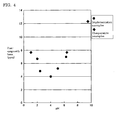
- the apparatus was set such that the range had 50 ppm at max and the edge exclusion was 2 mm. It should be noted that "haze” indicates a post-epigrowth haze average value (haze average). The results are shown in Fig. 4.
- the number of particles was measured for the substrate in Example 4 in which the rinse step was performed to rinse the substrate with the DI water to which the ultrasonic wave was being applied, and the substrate in Example 4 in which the rinse step was performed to rinse the substrate with the DI water to which the ultrasonic wave was not being applied.
- Surfscan 6220 of KLA Tencor was used to measure the number of particles.
- the number of particles indicates the number of particles having a size of ⁇ 0.265 ⁇ m or more per a substrate having a diameter of 50 mm.
- the results are tabulated in Table.
- Figure 4 is a graph showing a relationship between pH of the cleaning solution after the cleaning step (S20) and haze on the surface after the epitaxial growth.
- the vertical axis indicates haze (unit: ppm) on the surface of the substrate after the epitaxial growth
- the horizontal axis indicates pH of the cleaning solution (no unit of quantity).
- Comparative Examples 1 through 3 haze after the epitaxial growth showed 7.6 ppm, 7.6 ppm, and 12.3 ppm, respectively.
- haze on the surface of the substrate was increased because the surface treatment method was employed in which pH of the cleaning solution were 1, 6.4, and 9.5, which were out of the scope of the present invention.
- the table indicates results of the measurement of the number of particles on the substrates in Example 4, some of the substrates were rinsed with the DI water to which the ultrasonic wave was being applied in the substrate rinse step (ultrasonic wave ON), the other of the substrates were rinsed with the DI water to which the ultrasonic wave was not being applied (ultrasonic wave OFF). It should be noted that as the number of samplings (n count) twenty sites were measured.
- the number of particles on the substrate was 0.9 or less numbers per a substrate having a diameter of 50 mm, which was low.
- the number of particles was 0.9 or less number per a substrate having a diameter of 50 mm. It should be noted that in the cleaning step (S20) in Example 2, if the cleaning time was set to less than five seconds, actual cleaning times were varied enormously due to air intrusion into piping or the like. Therefore, by setting the cleaning time to be five seconds or more, the cleaning step (S20) was performed stably.
Landscapes
- Cleaning Or Drying Semiconductors (AREA)
- Crystals, And After-Treatments Of Crystals (AREA)
- Weting (AREA)
Abstract
Description
- The present invention relates to methods of surface treating substrates and to methods of manufacturing (Group) III-V compound semiconductors; in particular the invention relates to substrate surface treating and III-V compound semiconductor manufacturing methods that enable the reduction of post-epitaxial-growth surface roughness.
- Substrates composed of Group III-V semiconductor compounds have been widely used for semiconductor lasers, LEDs, and high-speed devices because they have luminescent properties and high electron mobility. Surface treatment is typically carried out in methods of manufacturing substrates composed of Group III-V semiconductor compounds. Such surface treatments include, for example, the surface treatment method disclosed in
Japanese Unexamined Pat. App. Pub. No. 2001-189278 Japanese Unexamined Pat. App. Pub. No. S62-252140 - In the surface treatment method disclosed in
Japanese Unexamined Pat. App. Pub. No. 2001-189278 - In the InP wafer cleaning method disclosed in
Japanese Unexamined Pat. App. Pub. No. S62-252140 - However, if the typical surface treatment method by an ozonated water process disclosed in Pat. App. Pub. No. 2001-189278 is applied to InP, the surface roughness of InP does not decrease. The reason is as follows. Ozonated water typically exhibits neutrality. If the surface treatment is performed with neutral ozonated water, the surface becomes Group III-rich because the stoichiometry (stoichiometric composition) of the surface of Group III-V is not optimum. As a result, in epitaxial growth the surface is likely to become roughened because Group III oxide hinders epitaxial growth.
- In the surface treatment of the front side of GaAs with ozonated water disclosed in
Japanese Unexamined Pat. App. Pub. No. 2001-189278 - In the method of cleaning the surface of InP wafer with a liquid mixture of phosphoric acid ― hydrogen peroxide ― water or a liquid mixture of hydrogen fluoride ― hydrogen peroxide ― water disclosed in
Japanese Unexamined Pat. App. Pub. No. S62-252140 Japanese Unexamined Pat. App. Pub. No. S62-252140 - An object of the present invention, in view of the circumstances noted above, is to make available a method of surface treating substrates and a method of manufacturing Group III-V compound semiconductors, in which the substrate composed of a Group III-V semiconductor compound is rendered stoichiometric and the microscopic roughness on the surface after the epitaxial growth is reduced.
- The present invention is a method of surface treating a substrate, comprising a step of preparing a substrate comprising Group III-V semiconductor compound; and a step of cleaning the substrate with a cleaning solution whose pH has been adjusted to be acidic from 2 to 6.3 inclusive and to which an oxidizing agent has been added.
- Since pH is adjusted to be from 2 to 6.3 inclusive, the surface of the substrate can be stoichiometric, thereby reducing haze on the surface of the substrate. Additionally, since the cleaning solution is DI water to which an oxidizing agent is added, the cleaning ability can be improved.
- In the substrate surface treating method involving the invention in another aspect, it is preferable that in the substrate preparation step the substrate prepared contain 5 mass % or more of indium.
- Accordingly, in the method of surface treating a substrate comprising a Group III-V semiconductor compound containing indium, the substrate is further stoichiometric to reduce the microscopic roughness on the surface.
- In a substrate surface treating method involving the invention in a further aspect, it is preferable that the cleaning time in the cleaning step is from 5 seconds to 60 seconds inclusive.
- Accordingly, even if the process is performed in a short time, the substrate comprising Group III-V compound semiconductor is stoichiometric, thereby reducing the microscopic roughness of the surface. Additionally, since the process can be performed in a short time, the cost of the processing solution can be reduced and the productivity can be improved.
- In a substrate surface treating method involving the invention in a further aspect, it is preferable that the method further comprises a pre-cleaning step, in advance of the cleaning step, of cleaning the substrate with an alkaline cleaning solution.
- Utilizing an alkaline cleaning solution in an pre-cleaning step thereby allows particles to be removed.
- In a substrate surface treating method involving the invention in a further aspect, it is preferable that the pre-cleaning step includes a water-wash substep of rinsing the substrate with DI water (Deionized Water).
- Since DI water is used for cleaning, the alkaline cleaning solution does not remain behind. As a result, unstable reactions, such as a neutralization reaction, during the acid wash are prevented and the effectiveness of the acid wash is not hindered, thereby shortening the acid wash time.
- In a substrate surface treating method involving the invention in a further aspect, it is preferable that the cleaning step includes a substep of rinsing the substrate with DI water.
- In a substrate surface treating method involving the invention in a further aspect, it is preferable that the rinsing step includes applying ultrasonic wave to the DI water.
- Accordingly, the clinging of particles to the substrate surface can be reduced.
- In a further aspect the invention is a method of manufacturing Group III-V compound semiconductor, comprising a step of implementing the above-described substrate surface treating method; and a step of depositing a film on the surface of the substrate after the step of implementing the substrate surface treating method.
- Accordingly, a Group III-V compound semiconductor is manufactured in which the substrate surface is stoichiometric and the microscopic roughness of the surface is reduced.
- According to the present invention, since pH of the cleaning solution is adjusted to be from 2 to 6.3 inclusive, the surface is stoichiometric, thereby reducing haze on the surface after the epitaxial growth. Additionally, since the cleaning solution is DI water to which an oxidizing agent is added, the cleaning ability can be improved.
- From the following detailed description in conjunction with the accompanying drawings, the foregoing and other objects, features, aspects and advantages of the present invention will become readily apparent to those skilled in the art.
-
- Fig. 1 is a flow chart showing a method of surface treating the substrate in Embodiment 1 of the present invention;
- Fig. 2 is a flow chart showing a method of surface treating the substrate in
Embodiment 2 of the present invention; - Fig. 3 is a schematic cross section of a cleaning apparatus used in a rinse step; and
- Fig. 4 is a graph showing a relationship between pH of the cleaning solution and haze following epitaxial growth.
- Hereinafter, referring to the figures, embodiments and examples of the present invention will be described. It should be understood that in the drawings accompanying the present description, identical reference marks are meant to indicate either identical or equivalent parts, and their explanation will not repeated.
- Figure 1 is a flow chart showing a method of surface treating a substrate in Embodiment 1 of the present invention. Referring to Fig. 1, the substrate surface treating method in Embodiment 1 of the present invention will be described.
- As shown in Fig. 1, a substrate preparation step (S10) is performed first in the substrate surface treating method in Embodiment 1, in which a substrate composed of Group III-V compound is prepared. The prepared substrate may be a bulk crystal or a thin film formed on a substrate made of a bulk crystal, for example.
- Next, a cleaning step (S20) is performed. In the cleaning step (S20), the substrate is cleaned with a cleaning solution whose pH has been adjusted to be acidic from 2 to 6.3 inclusive and to which an oxidizing agent has been added. It is preferable that as the cleaning solution a cleaning solution composed of DI water (a cleaning solution composed of DI water in which pH has been adjusted to be acidic from 2 to 6.3 inclusive, and an oxidizing agent has been added) is used. The use of the cleaning solution composed of the DI water prevents the surface of the substrate from being contaminated by impurities such as metal.
- In the step of adjusting pH of the cleaning solution, preferably, at least one selected from a group consisting of inorganic acid, organic acid, or water-soluble acid gas is contained in the DI water. Preferably, as the organic acid, formic acid, acetic acid, oxalic acid, lactic acid, malic acid, and citric acid are used. The reason is that it is easy to adjust pH of the cleaning solution to be about four because the organic acids are slightly acidic. It is preferable that as the water-soluble acid gases, for example, carbonic acid gas, hydrochloric gas (HCl), or hydrogen fluoride gas (HF) are used.
- As the oxidizing agents, hydrogen peroxide water is used, for example. The concentration of the oxidizing agent is in the range between 5 ppm and 1 mass %, for example, more preferably, between 10 ppm and 0.5 mass %. The reason is that if the concentration of oxidizing agent is under 5 ppm, the cleaning ability decreases, and if the concentration of the oxidizing agent is above 1 mass %, the oxidizing agent may react with an oxide, an organic material, or particles on the surface, thereby locally generating irregularities on the surface.
- Preferably, the cleaning time is, being not particularly restricted, in the range between five seconds to sixty seconds. The reason is that if the process is performed in a short time, the cleaning solution cost is reduced and the productivity is improved.
- The temperature of the cleaning solution is, being not particularly restricted, set to be room temperature. The reason is that equipment that surface treats a substrate is simplified by setting the temperature to be room temperature.
- Next, a post-treatment step (S30) is performed in which a deposition step (epitaxial growth) is performed on the substrate after the cleaning step (S20). In the post-treatment step (S30), the deposition step is performed in which a certain film is formed on a surface of the substrate composed of Group III-V compound semiconductor. It is preferable that a plurality of devices are formed on the substrate, in which the substrate would be divided into a plurality of devices by performing a dividing step, e.g., dicing such that a certain configuration is formed on the substrate surface and then the substrate is divided into individual elements. Accordingly, a device composed of Group III-V compound semiconductor is obtained. The device can be mounted on a lead frame, for example. Then, by performing a wire bonding step, a semiconductor device having the element is obtained.
- There are no particular restrictions on conditions of the substrate only if the substrate is composed of Group III-V compound semiconductor. It is preferable that the substrate includes 5 mass % or more of indium (In). For example, a compound semiconductor such as InP, InAs, InSb, and InN can be used. The reason is that if the substrate composed of these Group III-V compound semiconductors is surface treated with the substrate surface treating method in Embodiment 1, In oxide, which is difficult to be removed, is dissolved to make the surface more stoichiometric and decrease haze on the surface. In other words, the cleaning ability is improved.
- As described above, the substrate surface treating method in Embodiment 1 of the present invention includes the step (S10) of preparing a substrate composed of Group III-V compound semiconductor, and the cleaning step (S20) of cleaning the substrate with a cleaning solution whose pH has been adjusted to be from 2 to 6.3 inclusive and to which an oxidizing agent has been added. Since pH is adjusted to be more acidic, e.g., from 2 to 6.3 inclusive, the substrate surface is rendered stoichiometric. As a result, haze on the substrate after the epitaxial growth is decreased. In addition, since the oxidizing agent is added to the cleaning solution, the cleaning ability is improved.
- Figure 2 is a flow chart that shows a substrate surface treating method in
Embodiment 2 of the present invention. Referring to Fig. 2, the substrate surface treating method inEmbodiment 2 of the present invention will be described. - As shown in Fig. 2, the substrate surface treating method (cleaning method) in
Embodiment 2 has basically steps similar to those of the substrate surface treating method in Embodiment 1 of the present invention. - More specifically, in a pre-cleaning step (S40), before the cleaning step (S20), the substrate is cleaned with an alkaline cleaning solution. The pre-cleaning step (S40) may include a chemical cleaning step, a rinsing step (DI water rinsing step), and a drying step. The chemical cleaning step and the rinsing step (DI water rinsing step) can be repeated several times, if necessary.
- In the pre-cleaning step (S40), in order to remove impurities from the surface of the substrate composed of Group III-V compound semiconductor, any suitable manner can be used. For example, in the pre-cleaning step (S40), an alkaline cleaning solution is used. It is preferable that one is selected, as an alkaline cleaning solution, from a group consisting of aqueous sodium hydroxide (NaOH), aqueous potassium hydroxide (KOH), aqueous ammonia, and a cleaning solution including amines. The reason is that the alkaline cleaning solutions are effective in removing particles on the surface.
- As described above, the substrate surface treating method in
Embodiment 2 of the present invention includes the pre-cleaning step (S40) before the cleaning step (S20), in which the substrate is cleaned with the alkaline cleaning solution. The pre-cleaning step (S40) may include a rinsing step (DI water rinsing step) to clean the substrate with the DI water. As a result, in the pre-cleaning step (S40), particles can be removed with the alkaline cleaning solution. In the rinsing step, even if the alkaline cleaning solution is used in the pre-cleaning, haze on the surface of the substrate after the epitaxial growth is reduced because cleaning with the DI water does not leave the alkaline cleaning solution. - Referring to Fig. 2, a substrate surface treating method in
Embodiment 3 of the present invention will be described. As shown in Fig. 2, the substrate surface treating method (cleaning method) inEmbodiment 3 has basically steps similar to those of the substrate surface treating method inEmbodiment 2 of the present invention. - Specifically, the cleaning step (S20) includes a rinse step of cleaning the substrate with DI water to which ultrasonic wave is being applied. In the rinse step, vibrations or shaking is applied to the cleaning solution using a ultrasonic device, as shown in Fig. 3, for example.
- More specifically, the cleaning step (S20) may include a chemical cleaning step, a rinse step, and a drying step. The chemical cleaning step and the rinse step can be repeated several times, if required.
- Figure 3 is a schematic cross sectional view of showing a processing apparatus used for the rinse step. Referring to Fig. 3, the processing apparatus used for the substrate surface treating method according to the present invention will be described.
- As shown in Fig. 3, the processing apparatus includes a cleaning bath 1 that contains cleaning
solution 11 as rinse, an ultrasonicwave generation device 3 that is disposed on a bottom surface of the cleaning bath 1, and a controller 7 that is connected to the ultrasonicwave generation device 3 to control the ultrasonicwave generation device 3. Thecleaning solution 11 is contained in the cleaning bath 1. In addition, a plurality ofholders 13 for holding a plurality ofsubstrates 9 is immersed in thecleaning solution 11. Theholder 13 holds a plurality of thesubstrates 9 made of Group III-V compound semiconductor as objects of cleaning. The ultrasonicwave generation device 3 is located on the bottom surface of the cleaning bath 1. - When the substrate is cleaned in the rinse step, the
cleaning solution 11 is provided into the cleaning bath 1 as shown in Fig. 3 and thesubstrates 9 held by theholders 13 are immersed into thecleaning solution 11 together with theholders 13. As described above, the surface of thesubstrate 9 is cleaned with thecleaning solution 11. - The ultrasonic
wave generation device 3 can be controlled in the process by the controller 7 so as to produce ultrasonic wave, which is applied to thecleaning solution 11. Accordingly, thecleaning solution 11 vibrates, thereby increasing the effects of removing impurities or particles from thesubstrates 9. The cleaning bath 1 may be put on a member that can be shaken such as an XY stage, and by shaking the member the cleaning bath 1 can be shaken and thecleaning solution 11 inside can be stirred. Alternatively, thesubstrates 9 may be shaken together with theholder 13 by manual labor to stir thecleaning solution 11. In these cases, it is possible to increase the effect of removing impurities or particles from thesubstrate 9, likewise as applying the ultrasonic wave. - As described above, in the substrate surface treating method in
Embodiment 3 of the present invention, the cleaning step includes the rinse step of cleaning the substrate with DI water, and in the rinse step the ultrasonic wave is applied to the DI water. Although the particles are likely to be attached because the acidic cleaning solution (rinse) is used, by cleaning the substrate with the cleaning solution containing DI water to which the ultrasonic wave is being applied, it is possible to reduce the number of the particles attached to the surface of the substrate. The processing apparatus shown in Fig. 3 can be applied to other cleaning processes. - In order to confirm effects of the substrate surface treating method according to the present invention, samples were provided by Implementation Examples 1 through 5 and Comparative Examples 1 through 3, and the microscopic roughness and the number of particles on the sample surfaces were measured before and after the cleaning step. Prepared samples, measuring methods, and measurement results will be described hereinafter.
- First, a cleaning solution having a pH from 2 to 6.3 inclusive was prepared in order to optimize stoichiometry of the surface of a Group III-V compound semiconductor. Specifically, the following cleaning solutions were prepared by adding pH adjusting agents and oxidizing agents as well. In Implementation Examples 1 through 5 and Comparative Examples 1 through 3, pH adjusting agents and oxidizing agents employed the following materials. The pH value of the cleaning solution was measured by hydrogen-ion concentration measurement equipment, the calibration of which being performed with standard solutions having pH of 6.97 and 4.0.
- First, the substrate preparation step (S10) was performed. Specifically, as Group III-V compound semiconductor crystal, Fe-doped InP crystal was used. As InP crystal, InP crystal having a cylindrical shape with an outer diameter 50 mm was prepared. The crystal was wire-saw sliced at a plane orientation of (100) ± 1°. The substrate was lapped with SiC abrasive powder as hard abrasive, and then the substrate was etched with a liquid using acid and an oxidizing agent such as sulfuric acid, nitric acid, hydrochloric acid, and hydrogen peroxide. After that, one side of the substrate was finished with Br-methanol and polished. In the final polishing, the substrate was affixed to a glass plate with wax purified from turpentine.
- Next, the pre-cleaning step (S40) was performed. Specifically, after finishing polishing, alkali cleaning was carried out on the surface, and then the substrate was rinsed and peeled off from the plate. After that, the substrate was cleaned with the organic solvent and the alkali cleaning was carried out.
- Next, the cleaning step (S20) was performed. Specifically, ozone gas (concentration 15 ppm to 40 ppm) generated by electrolysis of the DI water as an oxidizing agent and carbonic acid gas as a pH adjusting agent were added to the deaired DI water so that the liquid would have a pH of 4. In a cleaning bath which provided the ozonated water whose pH had been adjusted, the above-mentioned InP substrate was cleaned for one minute. Then, as a rinse step, with the DI water with 17.5 MΩcm to 18.2 MΩcm to which the ultrasonic wave was not being applied, the substrate was cleaned for three minutes. After that, the substrate was dried in a vapor of isopropyl alcohol. Finally, the post-treatment step (S30) was performed. Specifically, the epitaxial growth was carried out on the substrate by a metal organic CVD system (MOCVD system). In Example 1, an InP film was grown on the Fe-doped InP substrate to be about 2 µm, an InGaAs film was grown to be about 4 µm, and an InP film was grown thereon to be about 1 µm.
- First, the substrate preparation step (S10) was performed. Specifically, Fe-doped InP crystal was used as crystal made of Group III-V compound semiconductor. As InP crystal, an InP crystal having a cylindrical shape with an outer diameter of 50 mm was prepared. The crystal was wire-saw sliced at a plane orientation of (100) ± 1°. The substrate was lapped with Al2O3 abrasive powder as hard abrasive, and then was etched with Br-methanol liquid. After that, one side of the substrate was polished using acidic colloidal silica and an oxidizing agent.
- Next, the pre-cleaning step (S40) was performed. Specifically, after the polishing, the substrate was cleaned with water, and acid and alkali cleaning were carried out. After that, the substrate was dried by a centrifugal drying apparatus.
- Next, the cleaning step (S20) was performed. Specifically, hydrochloric acid as a pH adjusting agent was added to hydrogen peroxide water with a dilution of 0.5% diluted with the DI water. In other words, the hydrogen peroxide water and the hydrochloric acid were added to the DI water so that the cleaning solution would have a pH of 2. Then, the wafer was set onto a rotatable stage and was rotated at 500 rpm, while being sprayed with the cleaning solution for eight seconds. Next, as a rinse step, the substrate was rinsed for twenty second with the DI water to which the ultrasonic wave was not being applied, and then the substrate was rotated at 1500 rpm to sputter the moisture for drying.
- Then, the post-treatment step (S30) was performed. Since the step (S30) was performed in a manner similar to that in Example 1, the description will not be repeated.
- First, the substrate preparation step (S10) was performed. Specifically, Fe-doped InP crystal as crystal made of Group III-V compound semiconductor was used. As InP crystal, InP crystal having a cylindrical shape with an outer diameter of 50 mm was prepared. Then, the crystal was wire-saw sliced at a plane orientation of (100) ± 1°, and the substrate was lapped by ceria abrasive powder as hard abrasive and then was etched by aqua regia.
- After that, one side of the substrate was polished with colloidal silica containing organic acid and a chlorine-based oxidizer.
- Next, the pre-cleaning step (S40) was performed. Since the step (S40) was similar to that in Example 2, the description will not be repeated.
- Next, the cleaning step (S20) was performed. Specifically, as a cleaning solution, ozonated water having a pH of 6.3 adjusted by the carbonic acid gas was used. Then, the wafer was set onto a rotatable stage and was rotated at 100 rpm ,while being sprayed with the cleaning solution for thirty seconds. Next, as a rinse step, the substrate was rinsed for twenty seconds with DI water to which the ultrasonic wave was not being applied, and then the substrate was rotated at 3000 rpm to sputter the moisture for drying. Finally, the post-treatment step (S30) was performed. Since the step (S30) was performed in a manner similar to that in Example 1, the description will not be repeated.
- First, the substrate preparation step (S10) was performed. Since the step (S10) was performed in a manner similar to that in Example 1, the description will not be repeated.
- Next, the pre-cleaning step (S40) was performed. Since the step (S40) was performed in a manner similar to that in Example 1, the description will not be repeated.
- Next, the cleaning step (S20) was performed. Specifically, the cleaning solution was manufactured by adding HF (hydrogen fluoride) as a pH adjusting agent to the DI water so that pH would be adjusted to be 2.4, and adding hydrogen peroxide water with a dilution ratio of 0.5% diluted with the DI water as an oxidizing agent. Then, in a cleaning bath supplying the cleaning solution, the above described InP substrate was cleaned for thirty seconds. Next, as a rinse step, the substrate was rinsed for twenty seconds with the DI water to which the ultrasonic wave was not being applied, and then the substrate was rotated at 3000 rpm to sputter the moisture for drying.
- It should be understood that in Example 4, as a rinse step, another substrate was manufactured by rinsing the substrate with the DI water to which the ultrasonic wave was being applied.
- Then, the post-treatment step (S30) was performed. Since the step (S30) was performed in a manner similar to that in Example 1, the description will not be repeated.
- First, the substrate preparation step (S10) was performed. Since the step (S10) was performed in a manner similar to that in Example 2, the description will not be repeated.
- Next, the pre-cleaning step (S40) was performed. The step (S40) was performed in a manner similar to that in Example 2, the description will not be repeated.
- Next, the cleaning step (S20) was performed. Specifically, the cleaning solution was manufactured by adding malic acid as a pH adjusting agent to the DI water so that pH would be 5.0, and adding hydrogen peroxide water having a dilution factor of 0.5% diluted with the DI water as an oxidizing agent. Then, in a cleaning bath supplying the cleaning solution, the above described InP substrate was cleaned for thirty seconds. Next, as a rinse step, the substrate was rinsed for twenty seconds with the DI water to which the ultrasonic wave was not being applied, and then the substrate was rotated at 3000 rpm to sputter the moisture for drying.
- Finally, the post-treatment step (S30) was performed. Since the step (S30) was performed in a manner similar to that in Example 1, the description will not be repeated.
- First, the substrate preparation step (S10) was performed. Since the step (S10) was performed in a manner similar to that in Example 3, the description will not be repeated.
- Next, the pre-cleaning step (S40) was performed. Since the step (S40) was performed in a manner similar to that in Example 3, the description will not repeated.
- Next, the cleaning step (S20) was performed. Specifically, the cleaning solution was manufactured by adding sulfuric acid as a pH adjusting agent to DI water so that pH would be 1.0, and adding hydrogen peroxide water having a dilution ratio of 0.5% diluted with DI water as an oxidizing agent. In a cleaning bath supplying the cleaning solution, the above described InP substrate was cleaned for thirty seconds. Next, as a rinse step, the substrate was rinsed for twenty seconds with DI water to which the ultrasonic wave was not being applied, and then the substrate was rotated at 3000 rpm to sputter the moisture for drying.
- Finally, the post-treatment step (S30) was performed. Since the step (S30) was performed in a manner similar to that in Example 1, the description will not be repeated.
- First, the substrate preparation step (S10) was performed. The step (S10) was performed in a manner similar to that in Example 1, the description will not be repeated.
- Next, the pre-cleaning step (S40) was performed. Since the step (S40) was performed in a manner similar to that in Example 1, the description will not be repeated.
- Next, the cleaning step (S20) was performed. Specifically, the cleaning solution was manufactured by adding hydrogen peroxide water having a dilution ratio of 0.5% diluted with DI water as an oxidizing agent to DI water having a pH of 6.4, without using a pH adjusting agent. Then, in a cleaning bath supplying the cleaning solution, the above described InP substrate was cleaned for thirty seconds.
- Next, as a rinse step, the substrate was rinsed for twenty seconds with the DI water to which the ultrasonic wave was not being applied, and the substrate was rotated at 3000 rpm to sputter the moisture for drying.
- Finally, the post-treatment step (S30) was performed. Since the step (S30) was performed in a manner similar to that in Example 1, the description will not be repeated.
- First, the substrate preparation step (S10) was performed. Since the step (S10) was performed in a manner similar to that in Example 2, the description will not be repeated.
- Next, the pre-cleaning step (S40) was performed. Since the step (S40) was performed in a manner similar to that in Example 2, the description will not be repeated.
- Next, the cleaning step (S20) was performed. Specifically, the cleaning solution was manufactured by adding ammonia as a pH adjusting agent to the DI water so that pH would be 9.5, and adding hydrogen peroxide water having a dilution ratio of 0. 5% diluted with DI water as an oxidizing agent. Then, in a cleaning bath supplying the cleaning solution, the above described InP substrate was cleaned for thirty seconds. Next, as a rinse step, the substrate was rinsed for twenty seconds with the DI water to which the ultrasonic wave was not being applied, and then the substrate was rotated at 3000 rpm to sputter the moisture for drying.
- Finally, the post-treatment step (S30) was performed. Since the step (S30) was performed in a manner similar to that in Example 1, the description will not be repeated.
- Micro-roughness (haze) on the surface was measured for substrates in Implementation Examples 1 and 2, and Comparative Example 1 after the epitaxial growth. Surfscan 6220 of KLA Tencor was used to measure haze. The apparatus was set such that the range had 50 ppm at max and the edge exclusion was 2 mm. It should be noted that "haze" indicates a post-epigrowth haze average value (haze average). The results are shown in Fig. 4.
- The number of particles was measured for the substrate in Example 4 in which the rinse step was performed to rinse the substrate with the DI water to which the ultrasonic wave was being applied, and the substrate in Example 4 in which the rinse step was performed to rinse the substrate with the DI water to which the ultrasonic wave was not being applied. Surfscan 6220 of KLA Tencor was used to measure the number of particles. The number of particles indicates the number of particles having a size of φ 0.265 µm or more per a substrate having a diameter of 50 mm. The results are tabulated in Table.
Table Ultrasonic wave ON Ultrasonic wave OFF Average (number/50 mm dia.) 0.9 2.0 Standard deviation 1.0 1.8 No. of samplings 20 20 - Figure 4 is a graph showing a relationship between pH of the cleaning solution after the cleaning step (S20) and haze on the surface after the epitaxial growth. In Fig. 4, the vertical axis indicates haze (unit: ppm) on the surface of the substrate after the epitaxial growth, and the horizontal axis indicates pH of the cleaning solution (no unit of quantity).
- As shown in Fig. 4, post-epigrowth haze exhibited in Implementation Examples 1 through 5 was 4 ppm, 6.7 ppm, 7.0 ppm, 4.8 ppm, and 5.2 ppm, respectively. In Implementation Examples 1 through 5, haze on the surface of the substrate was decreased by employing a surface treatment method in which pH of the cleaning solution was from 2 to 6.3 inclusive, which were in the scope of the present invention.
- In contrast, in Comparative Examples 1 through 3, haze after the epitaxial growth showed 7.6 ppm, 7.6 ppm, and 12.3 ppm, respectively. In Comparative Examples 1 through 3, haze on the surface of the substrate was increased because the surface treatment method was employed in which pH of the cleaning solution were 1, 6.4, and 9.5, which were out of the scope of the present invention.
- Furthermore, the table indicates results of the measurement of the number of particles on the substrates in Example 4, some of the substrates were rinsed with the DI water to which the ultrasonic wave was being applied in the substrate rinse step (ultrasonic wave ON), the other of the substrates were rinsed with the DI water to which the ultrasonic wave was not being applied (ultrasonic wave OFF). It should be noted that as the number of samplings (n count) twenty sites were measured.
- As shown in Table, the number of particles on the substrate (ultrasonic wave ON) was 0.9 or less numbers per a substrate having a diameter of 50 mm, which was low. In the substrate (ultrasonic wave OFF), the number of particles was 0.9 or less number per a substrate having a diameter of 50 mm. It should be noted that in the cleaning step (S20) in Example 2, if the cleaning time was set to less than five seconds, actual cleaning times were varied enormously due to air intrusion into piping or the like. Therefore, by setting the cleaning time to be five seconds or more, the cleaning step (S20) was performed stably.
- The presently disclosed Embodiments and Implementation Examples should in all respects be considered to be illustrative and not limiting. The scope of the present invention is set forth not by the foregoing description but by the scope of the patent claims, and is intended to include meanings equivalent to the scope of the patent claims and all modifications within the scope.
Claims (8)
- A method of surface treating a substrate, comprising:a step of preparing a substrate composed of a Group III-V semiconductor compound; anda cleaning step of cleaning the substrate with a cleaning solution whose pH has been adjusted to an acidity of 2 to 6.3 inclusive and to which an oxidizing agent has been added.
- A substrate surface treating method as set forth in claim 1, wherein the prepared substrate contains 5 mass % or more of indium.
- A substrate surface treating method as set forth in claim 1 or 2, wherein the cleaning time is from 5 seconds to 60 seconds inclusive.
- A substrate surface treating method as set forth in any of claims 1 through 3, further comprising a pre-cleaning step, in advance of said cleaning step, of cleaning the substrate using an alkaline cleaning solution.
- A substrate surface treating method as set forth in claim 4, wherein said pre-cleaning step includes a water-wash step of rinsing the substrate with DI water.
- A substrate surface treating method as set forth in any of claims 1 through 5, wherein said cleaning step includes a rinsing step of rinsing the substrate with DI water.
- A substrate surface treating method as set forth in claim 6, wherein the rinsing step includes applying ultrasonic wave to the DI water.
- A method of manufacturing a Group III-V compound semiconductor, comprising:implementing a substrate surface treating method as set forth in any of claims 1 through 7; anddepositing a film on the surface of the substrate after implementing the substrate surface treating method.
Applications Claiming Priority (1)
| Application Number | Priority Date | Filing Date | Title |
|---|---|---|---|
| JP2005182217A JP2007005472A (en) | 2005-06-22 | 2005-06-22 | Substrate surface treatment method and III-V compound semiconductor manufacturing method |
Publications (2)
| Publication Number | Publication Date |
|---|---|
| EP1737026A1 true EP1737026A1 (en) | 2006-12-27 |
| EP1737026B1 EP1737026B1 (en) | 2009-04-22 |
Family
ID=36821871
Family Applications (1)
| Application Number | Title | Priority Date | Filing Date |
|---|---|---|---|
| EP06012051A Not-in-force EP1737026B1 (en) | 2005-06-22 | 2006-06-12 | Method of surface treating III-V semiconductor compound based substrates and method of manufacturing III-V compound semiconductors |
Country Status (7)
| Country | Link |
|---|---|
| US (1) | US7432186B2 (en) |
| EP (1) | EP1737026B1 (en) |
| JP (1) | JP2007005472A (en) |
| KR (1) | KR20060134810A (en) |
| CN (1) | CN1885499A (en) |
| DE (1) | DE602006006370D1 (en) |
| TW (1) | TW200703485A (en) |
Cited By (2)
| Publication number | Priority date | Publication date | Assignee | Title |
|---|---|---|---|---|
| EP1830397A3 (en) * | 2006-03-02 | 2009-09-16 | Sumitomo Electric Industries, Ltd. | Surface treatment method of compound semiconductor substrate, fabrication method of compound semiconductor, compound semiconductor substrate, and semiconductor wafer |
| EP3139416B1 (en) * | 2015-09-07 | 2020-10-28 | IMEC vzw | Texturing monocrystalline silicon substrates |
Families Citing this family (21)
| Publication number | Priority date | Publication date | Assignee | Title |
|---|---|---|---|---|
| TWI410422B (en) | 2007-01-15 | 2013-10-01 | Mitsubishi Tanabe Pharma Corp | Condensed tetrahydroquinoline derivative and its medical use |
| JP4934079B2 (en) * | 2008-02-28 | 2012-05-16 | 信越半導体株式会社 | Ultrasonic cleaning apparatus and ultrasonic cleaning method |
| JP4697272B2 (en) * | 2008-07-18 | 2011-06-08 | 住友電気工業株式会社 | III-V compound semiconductor substrate manufacturing method and epitaxial wafer manufacturing method |
| US8226772B2 (en) * | 2009-01-08 | 2012-07-24 | Micron Technology, Inc. | Methods of removing particles from over semiconductor substrates |
| JP5471001B2 (en) | 2009-04-20 | 2014-04-16 | 住友電気工業株式会社 | Indium phosphide substrate manufacturing method, epitaxial wafer manufacturing method, indium phosphide substrate, and epitaxial wafer |
| EP2337089A3 (en) * | 2009-12-17 | 2013-12-11 | Rohm and Haas Electronic Materials LLC | Improved method of texturing semiconductor substrates |
| WO2012002440A1 (en) * | 2010-06-29 | 2012-01-05 | 京セラ株式会社 | Method for surface-treating semiconductor substrate, semiconductor substrate, and method for producing solar battery |
| CN102468125B (en) * | 2010-11-01 | 2015-10-14 | 中芯国际集成电路制造(上海)有限公司 | A kind of cleaning method of wafer |
| CN102956450B (en) * | 2011-08-16 | 2015-03-11 | 中芯国际集成电路制造(北京)有限公司 | Method for manufacturing semiconductor devices |
| US20130068248A1 (en) * | 2011-09-15 | 2013-03-21 | Taiwan Semiconductor Manufacturing Company, Ltd., ("Tsmc") | Semiconductor device cleaning method |
| CN102456549B (en) * | 2011-11-08 | 2014-06-25 | 北京通美晶体技术有限公司 | Indium phosphide wafer and surface cleaning method thereof |
| US9105578B2 (en) * | 2013-03-12 | 2015-08-11 | Taiwan Semiconductor Manufacturing Company, Ltd. | Interface for metal gate integration |
| US9263275B2 (en) | 2013-03-12 | 2016-02-16 | Taiwan Semiconductor Manufacturing Company, Ltd. | Interface for metal gate integration |
| CN103236396B (en) * | 2013-04-16 | 2016-07-06 | 中国电子科技集团公司第十一研究所 | A kind of surface treatment method of extension InSb substrate |
| US9280998B1 (en) | 2015-03-30 | 2016-03-08 | WD Media, LLC | Acidic post-sputter wash for magnetic recording media |
| TWI586444B (en) * | 2015-09-09 | 2017-06-11 | 日月光半導體製造股份有限公司 | Cleaning device and detergent solution for cleaning ic substrate conveyer roller |
| CN105710066B (en) * | 2016-03-16 | 2018-03-13 | 中锗科技有限公司 | A kind of method for removing solar energy single germanium wafer polishing residual medicament |
| JP6918600B2 (en) * | 2016-07-29 | 2021-08-11 | 芝浦メカトロニクス株式会社 | Processing liquid generator and substrate processing equipment using it |
| EP3514266B1 (en) * | 2017-05-26 | 2025-10-15 | Sumitomo Electric Industries, Ltd. | Group iii v compound semiconductor substrate and group iii v compound semiconductor substrate with epitaxial layer |
| CN115020218B (en) * | 2022-07-01 | 2025-10-24 | 广东先导微电子科技有限公司 | A surface treatment method for indium phosphide wafer |
| WO2025203466A1 (en) * | 2024-03-28 | 2025-10-02 | 住友電気工業株式会社 | Indium phosphide substrate and method for manufacturing indium phosphide substrate |
Citations (3)
| Publication number | Priority date | Publication date | Assignee | Title |
|---|---|---|---|---|
| EP0617458A2 (en) * | 1993-03-19 | 1994-09-28 | Mitsubishi Denki Kabushiki Kaisha | Etching solution and etching method for semiconductor therefor |
| JP2001044169A (en) * | 1999-05-25 | 2001-02-16 | Sharp Corp | Semiconductor etchant, preparation method and etching method |
| EP1530232A2 (en) * | 2003-10-20 | 2005-05-11 | Air Products And Chemicals, Inc. | Process solutions containing surfactants used as post-chemical mechanical planarization treatment |
Family Cites Families (8)
| Publication number | Priority date | Publication date | Assignee | Title |
|---|---|---|---|---|
| JPS62252140A (en) * | 1986-04-25 | 1987-11-02 | Nippon Mining Co Ltd | Cleaning method for inp wafer |
| JP3422117B2 (en) * | 1994-01-28 | 2003-06-30 | 和光純薬工業株式会社 | New surface treatment method and treatment agent |
| US5763016A (en) * | 1996-12-19 | 1998-06-09 | Anon, Incorporated | Method of forming patterns in organic coatings films and layers |
| JPH11111703A (en) * | 1997-09-30 | 1999-04-23 | Akihiko Yoshikawa | Method for etching II-VI compound semiconductor |
| JP4110220B2 (en) | 1999-12-28 | 2008-07-02 | Dowaエレクトロニクス株式会社 | Method of surface treatment of compound semiconductor substrate or base film, compound semiconductor substrate having compound single crystal film, and semiconductor device |
| JP4752117B2 (en) * | 2001-02-08 | 2011-08-17 | 日本テキサス・インスツルメンツ株式会社 | Method for removing particles on a semiconductor wafer |
| JP2003174021A (en) * | 2001-12-06 | 2003-06-20 | Sharp Corp | Method for selective etching of semiconductor substrate |
| US7259084B2 (en) * | 2003-07-28 | 2007-08-21 | National Chiao-Tung University | Growth of GaAs epitaxial layers on Si substrate by using a novel GeSi buffer layer |
-
2005
- 2005-06-22 JP JP2005182217A patent/JP2007005472A/en active Pending
-
2006
- 2006-06-09 TW TW095120505A patent/TW200703485A/en unknown
- 2006-06-12 DE DE602006006370T patent/DE602006006370D1/en not_active Expired - Fee Related
- 2006-06-12 EP EP06012051A patent/EP1737026B1/en not_active Not-in-force
- 2006-06-19 KR KR1020060054843A patent/KR20060134810A/en not_active Withdrawn
- 2006-06-21 US US11/425,394 patent/US7432186B2/en not_active Expired - Fee Related
- 2006-06-21 CN CNA2006100940169A patent/CN1885499A/en active Pending
Patent Citations (3)
| Publication number | Priority date | Publication date | Assignee | Title |
|---|---|---|---|---|
| EP0617458A2 (en) * | 1993-03-19 | 1994-09-28 | Mitsubishi Denki Kabushiki Kaisha | Etching solution and etching method for semiconductor therefor |
| JP2001044169A (en) * | 1999-05-25 | 2001-02-16 | Sharp Corp | Semiconductor etchant, preparation method and etching method |
| EP1530232A2 (en) * | 2003-10-20 | 2005-05-11 | Air Products And Chemicals, Inc. | Process solutions containing surfactants used as post-chemical mechanical planarization treatment |
Non-Patent Citations (3)
| Title |
|---|
| GUIVARC'H A ET AL: "CHEMICAL CLEANING OF INP SURFACES: OXIDE COMPOSITION AND ELECTRICALPROPERTIES", JOURNAL OF APPLIED PHYSICS, AMERICAN INSTITUTE OF PHYSICS. NEW YORK, US, vol. 55, no. 4, February 1984 (1984-02-01), pages 1139 - 1148, XP000819836, ISSN: 0021-8979 * |
| OLIVIER J ET AL INSTITUTE OF PHYSICS: "CHEMICAL CLEANING PROCEDURES OF GAAS (100) SURFACES STUDIED BY X-RAY PHOTOELECTRON SPECTROSCOPY", GALLIUM ARSENIDE AND RELATED COMPOUNDS. JERSEY, 24 - 27 SEPT., 1990, PROCEEDINGS OF THE INTERNATIONAL SYMPOSIUM ON GALLIUM ARSENIDE AND RELATED COMPOUNDS. (TITLE FROM 1994 ONWARDS: PROCEEDINGS OF THE INTERNATIONAL SYMPOSIUM ON COMPOUND SEMICONDUCTORS, vol. SYMP. 17, 24 September 1990 (1990-09-24), pages 305 - 310, XP000146779 * |
| PATENT ABSTRACTS OF JAPAN vol. 2000, no. 19 5 June 2001 (2001-06-05) * |
Cited By (2)
| Publication number | Priority date | Publication date | Assignee | Title |
|---|---|---|---|---|
| EP1830397A3 (en) * | 2006-03-02 | 2009-09-16 | Sumitomo Electric Industries, Ltd. | Surface treatment method of compound semiconductor substrate, fabrication method of compound semiconductor, compound semiconductor substrate, and semiconductor wafer |
| EP3139416B1 (en) * | 2015-09-07 | 2020-10-28 | IMEC vzw | Texturing monocrystalline silicon substrates |
Also Published As
| Publication number | Publication date |
|---|---|
| CN1885499A (en) | 2006-12-27 |
| KR20060134810A (en) | 2006-12-28 |
| TW200703485A (en) | 2007-01-16 |
| US20070014915A1 (en) | 2007-01-18 |
| US7432186B2 (en) | 2008-10-07 |
| JP2007005472A (en) | 2007-01-11 |
| EP1737026B1 (en) | 2009-04-22 |
| DE602006006370D1 (en) | 2009-06-04 |
Similar Documents
| Publication | Publication Date | Title |
|---|---|---|
| EP1737026B1 (en) | Method of surface treating III-V semiconductor compound based substrates and method of manufacturing III-V compound semiconductors | |
| TWI520203B (en) | Method for inspecting compound semiconductor substrate, compound semiconductor substrate, surface treatment method of compound semiconductor substrate, and method for producing compound semiconductor crystal | |
| EP1997587B1 (en) | Method of polishing compound semiconductor substrate and method of manufacturing compound semiconductor epitaxial substrate | |
| EP1830397A2 (en) | Surface treatment method of compound semiconductor substrate, fabrication method of compound semiconductor, compound semiconductor substrate, and semiconductor wafer | |
| US20030186028A1 (en) | Epitaxially coated semiconductor wafer and process for producing it | |
| KR20170033317A (en) | Method for cleaning compound semiconductor and solution for cleaning of compound semiconductor | |
| US20030010280A1 (en) | Epitaxial semiconductor wafer and a manufacturing method thereof | |
| JP4857738B2 (en) | Semiconductor wafer cleaning method and manufacturing method | |
| KR20110036990A (en) | Uniform oxide film formation method and cleaning method | |
| US20040266191A1 (en) | Process for the wet-chemical surface treatment of a semiconductor wafer | |
| JPH0786220A (en) | Semiconductor wafer cleaning method | |
| US20090203212A1 (en) | Surface Grinding Method and Manufacturing Method for Semiconductor Wafer | |
| JPH1116844A (en) | Manufacturing method of epitaxial silicon wafer and wafer for material | |
| KR102109893B1 (en) | Bonded wafer manufacturing method | |
| JP3595681B2 (en) | Manufacturing method of epitaxial wafer | |
| JPH11283924A (en) | Semiconductor wafer manufacturing method | |
| JP3036366B2 (en) | Processing method of semiconductor silicon wafer | |
| JP2001213696A (en) | Manufacturing method of epitaxyial wafer and its semiconductor manufacturing equipment | |
| DE10212657A1 (en) | Wet chemical cleaning of a silicon wafer comprises initially contacting a hydrophobic surface partially covered with polishing agent, and contacting with an aqueous solution containing an oxidant | |
| JP4306217B2 (en) | Method for drying semiconductor substrate after cleaning | |
| JP3718419B2 (en) | Manufacturing method of silicon epitaxial wafer | |
| KR100235944B1 (en) | Method of Cleaning Semiconductor Devices | |
| RU2537743C1 (en) | Method for pre-epitaxial treatment of surface of germanium substrate | |
| CN116798853A (en) | A method for growing silicon epitaxial wafers | |
| KR100219071B1 (en) | Semiconductor Wafer Cleaning Method |
Legal Events
| Date | Code | Title | Description |
|---|---|---|---|
| PUAI | Public reference made under article 153(3) epc to a published international application that has entered the european phase |
Free format text: ORIGINAL CODE: 0009012 |
|
| AK | Designated contracting states |
Kind code of ref document: A1 Designated state(s): AT BE BG CH CY CZ DE DK EE ES FI FR GB GR HU IE IS IT LI LT LU LV MC NL PL PT RO SE SI SK TR |
|
| AX | Request for extension of the european patent |
Extension state: AL BA HR MK YU |
|
| 17P | Request for examination filed |
Effective date: 20070125 |
|
| 17Q | First examination report despatched |
Effective date: 20070222 |
|
| AKX | Designation fees paid |
Designated state(s): DE FR GB |
|
| GRAP | Despatch of communication of intention to grant a patent |
Free format text: ORIGINAL CODE: EPIDOSNIGR1 |
|
| RIC1 | Information provided on ipc code assigned before grant |
Ipc: H01L 21/02 20060101AFI20081110BHEP |
|
| GRAS | Grant fee paid |
Free format text: ORIGINAL CODE: EPIDOSNIGR3 |
|
| GRAA | (expected) grant |
Free format text: ORIGINAL CODE: 0009210 |
|
| AK | Designated contracting states |
Kind code of ref document: B1 Designated state(s): DE FR GB |
|
| REG | Reference to a national code |
Ref country code: GB Ref legal event code: FG4D |
|
| REF | Corresponds to: |
Ref document number: 602006006370 Country of ref document: DE Date of ref document: 20090604 Kind code of ref document: P |
|
| PGFP | Annual fee paid to national office [announced via postgrant information from national office to epo] |
Ref country code: FR Payment date: 20090608 Year of fee payment: 4 |
|
| PGFP | Annual fee paid to national office [announced via postgrant information from national office to epo] |
Ref country code: DE Payment date: 20090730 Year of fee payment: 4 |
|
| PLBE | No opposition filed within time limit |
Free format text: ORIGINAL CODE: 0009261 |
|
| STAA | Information on the status of an ep patent application or granted ep patent |
Free format text: STATUS: NO OPPOSITION FILED WITHIN TIME LIMIT |
|
| 26N | No opposition filed |
Effective date: 20100125 |
|
| GBPC | Gb: european patent ceased through non-payment of renewal fee |
Effective date: 20100612 |
|
| REG | Reference to a national code |
Ref country code: FR Ref legal event code: ST Effective date: 20110228 |
|
| PG25 | Lapsed in a contracting state [announced via postgrant information from national office to epo] |
Ref country code: DE Free format text: LAPSE BECAUSE OF NON-PAYMENT OF DUE FEES Effective date: 20110101 |
|
| PG25 | Lapsed in a contracting state [announced via postgrant information from national office to epo] |
Ref country code: FR Free format text: LAPSE BECAUSE OF NON-PAYMENT OF DUE FEES Effective date: 20100630 |
|
| PG25 | Lapsed in a contracting state [announced via postgrant information from national office to epo] |
Ref country code: GB Free format text: LAPSE BECAUSE OF NON-PAYMENT OF DUE FEES Effective date: 20100612 |