EP1735967B1 - Zustandscodierung in mehrbit-flash-zellen - Google Patents
Zustandscodierung in mehrbit-flash-zellen Download PDFInfo
- Publication number
- EP1735967B1 EP1735967B1 EP05709145.6A EP05709145A EP1735967B1 EP 1735967 B1 EP1735967 B1 EP 1735967B1 EP 05709145 A EP05709145 A EP 05709145A EP 1735967 B1 EP1735967 B1 EP 1735967B1
- Authority
- EP
- European Patent Office
- Prior art keywords
- bit
- bits
- reading
- threshold voltage
- comparisons
- Prior art date
- Legal status (The legal status is an assumption and is not a legal conclusion. Google has not performed a legal analysis and makes no representation as to the accuracy of the status listed.)
- Expired - Lifetime
Links
- 238000000034 method Methods 0.000 claims description 43
- 230000003068 static effect Effects 0.000 claims description 25
- 230000015654 memory Effects 0.000 claims description 20
- 230000008569 process Effects 0.000 claims description 8
- 230000007704 transition Effects 0.000 description 50
- 238000011156 evaluation Methods 0.000 description 10
- 238000013461 design Methods 0.000 description 5
- 238000009826 distribution Methods 0.000 description 5
- 238000010586 diagram Methods 0.000 description 3
- 230000004044 response Effects 0.000 description 2
- 229930091051 Arenine Natural products 0.000 description 1
- 101100394497 Caenorhabditis elegans toe-1 gene Proteins 0.000 description 1
- XUIMIQQOPSSXEZ-UHFFFAOYSA-N Silicon Chemical group [Si] XUIMIQQOPSSXEZ-UHFFFAOYSA-N 0.000 description 1
- 238000004458 analytical method Methods 0.000 description 1
- 238000013459 approach Methods 0.000 description 1
- 230000006399 behavior Effects 0.000 description 1
- 230000009286 beneficial effect Effects 0.000 description 1
- 238000005352 clarification Methods 0.000 description 1
- 238000010276 construction Methods 0.000 description 1
- 230000007547 defect Effects 0.000 description 1
- 230000006872 improvement Effects 0.000 description 1
- 239000012535 impurity Substances 0.000 description 1
- 238000012986 modification Methods 0.000 description 1
- 230000004048 modification Effects 0.000 description 1
- 238000005457 optimization Methods 0.000 description 1
- 230000009467 reduction Effects 0.000 description 1
- 239000004065 semiconductor Substances 0.000 description 1
- 229910052710 silicon Inorganic materials 0.000 description 1
- 239000010703 silicon Substances 0.000 description 1
Images


Classifications
-
- G—PHYSICS
- G11—INFORMATION STORAGE
- G11C—STATIC STORES
- G11C16/00—Erasable programmable read-only memories
- G11C16/02—Erasable programmable read-only memories electrically programmable
- G11C16/04—Erasable programmable read-only memories electrically programmable using variable threshold transistors, e.g. FAMOS
-
- G—PHYSICS
- G11—INFORMATION STORAGE
- G11C—STATIC STORES
- G11C16/00—Erasable programmable read-only memories
- G11C16/02—Erasable programmable read-only memories electrically programmable
- G11C16/06—Auxiliary circuits, e.g. for writing into memory
- G11C16/10—Programming or data input circuits
-
- G—PHYSICS
- G11—INFORMATION STORAGE
- G11C—STATIC STORES
- G11C11/00—Digital stores characterised by the use of particular electric or magnetic storage elements; Storage elements therefor
- G11C11/56—Digital stores characterised by the use of particular electric or magnetic storage elements; Storage elements therefor using storage elements with more than two stable states represented by steps, e.g. of voltage, current, phase, frequency
- G11C11/5621—Digital stores characterised by the use of particular electric or magnetic storage elements; Storage elements therefor using storage elements with more than two stable states represented by steps, e.g. of voltage, current, phase, frequency using charge storage in a floating gate
- G11C11/5628—Programming or writing circuits; Data input circuits
-
- G—PHYSICS
- G11—INFORMATION STORAGE
- G11C—STATIC STORES
- G11C7/00—Arrangements for writing information into, or reading information out from, a digital store
- G11C7/10—Input/output [I/O] data interface arrangements, e.g. I/O data control circuits, I/O data buffers
- G11C7/1006—Data managing, e.g. manipulating data before writing or reading out, data bus switches or control circuits therefor
Definitions
- the present invention relates to flash memories and, more particularly, to a method of storing data in multi-bit flash cells.
- Flash memory devices have been known for many years. Typically, each cell within a flash memory stores one bit of information. Traditionally, the way to store a bit has been by supporting two states of the cell - one state represents a logical "0" and the other state represents a logical "1". In a flash memory cell the two states are implemented by having a floating gate above the cell's channel (the area connecting the source and drain elements of the cell's transistor), and having two valid states for the amount of charge stored within this floating gate. Typically, one state is with zero charge in the floating gate and is the initial unwritten state of the cell after being erased (commonly defined to represent the "1" state) and another state is with some amount of negative charge in the floating gate (commonly defined to represent the "0" state).
- the threshold voltage of the cell's transistor i.e . the voltage that has to be applied to the transistor's control gate in order to cause the transistor to conduct
- the threshold voltage of the cell's transistor i.e . the voltage that has to be applied to the transistor's control gate in order to cause the transistor to conduct
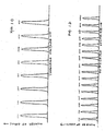
- Figure 1A shows graphically how this works. Specifically, Figure 1A shows the distribution of the threshold voltages of a large population of cells. Because the cells in a flash device are not exactly identical in their characteristics and behavior (due, for example, to small variations in impurities concentrations or to defects in the silicon structure), applying the same programming operation to all the cells does not cause all of the cells to have exactly the same threshold voltage. (Note that, for historical reasons, writing data to a flash memory is commonly referred to as "programming" the flash memory.) Instead, the threshold voltage is distributed similar to the way shown in Figure 1A .
- Cells storing a value of "1" typically have a negative threshold voltage, such that most of the cells have a threshold voltage close to the value shown by the left peak of Figure 1A , with some smaller numbers of cells having lower or higher threshold voltages.
- cells storing a value of "0" typically have a positive threshold voltage, such that most of the cells have a threshold voltage close to the value shown by the right peak of Figure 1A , with some smaller numbers of cells having lower or higher threshold voltages.
- FIG. 1B shows the threshold voltage distribution for a typical 2-bit MBC cell. As expected, Figure IB has four peaks, each corresponding to one state. As for the SBC case, each state is actually a range and not a single number. When reading the cell's contents, all that must be guaranteed is that the range that the cell's threshold voltage is in is correctly identified. For a prior art example of an MBC flash device see US Patent No. 5,434,825 to Harari .
- Figure 1C shows the threshold voltage distribution for a typical 3-bit MBC cell. As expected, Figure 1C has eight peaks, each corresponding to one state.
- Figure ID shows the threshold voltage distribution for a 4-bit MBC cell, for which sixteen states, represented by sixteen threshold voltage ranges, are required.
- the range that the cell's threshold voltage is in must be identified correctly; only in this case this cannot always be achieved by comparing to only one reference voltage. Instead, several comparisons may be necessary. For example, in the case illustrated in Figure 1B , to read the lower bit,_the cell's threshold voltage first is compared to a reference comparison voltage V 1 and then, depending on the outcome of the comparison, to either a zero reference comparison voltage or a reference comparison voltage V 2 . Alternatively, the lower bit is read by unconditionally comparing the threshold voltage to both a zero reference voltage and a reference comparison voltage V 2 , again requiring two comparisons. For more than two bits per cell, even more comparisons might be required.
- the bits of a single MBC cell may all belong to the same flash page, or they may be assigned to different pages so that, for example in a 4-bit cell, the lowest bit is in page 0, the next bit is in page 1, the next bit in page 2, and the highest bit is in page 3. (A page is the smallest portion of data that can be separately written in a flash device). Both method are in use. While the methods of the present invention are explained here in the context of the "each, bit in its own page" approach, these methods also can be aplied to the case of all bits residing in the same page.
- N Factorial N Factorial
- the left-most state always corresponds to the "all ones" bit pattern.
- programming can only increase the threshold voltage of a cell, not reduce it. Reduction of the threshold voltage can only be done when erasing, but erasing can be applied only to large groups of cells ("blocks" in common terminology). Therefore, any ordering of the bit patterns that requires the threshold voltage to decrease when writing a bit to "0" cannot be used.
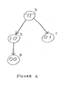
- Figure 2 shows a graphical representation of the restrictions applicable to the ordering of bit patterns in a 2-bit MBC cell. Each bit pattern is shown by its binary representation within a circle, and by its decimal representation outside the circle. Both numerical representations are equivalent, but it is more convenient to use the binary representation for understanding the ordering restrictions, and to use the decimal representation for talking about a certain pattern.
- An arrow connecting two circles in Figure 2 means that the state from which the arrow originates must precede the state to which the arrow points.
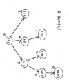
- Figure 3 shows the corresponding graphical representation for the case of 3-bit MBC cells
- Figure 4 shows the corresponding graphical representation for the case of 4-bit MBC cells. Both cases are much more complex than the 2-bit case and allow many more valid orderings.
- Appendices list 3-bit and 4-bit orderings along with analyses of these orderings, as described below.
- Appendix A lists all 315 3-bit orderings.
- Appendices B,C,D and E are partial lists of the 4-bit orderings.
- US 2002/114194 A1 discloses a multilevel storage non-volatile semiconductor memory device enabling high-speed data reading and high-speed data writing.
- Each memory cell can hold data of n bits in correspondence to 2 n threshold levels.
- Figs. 42 and 43 illustrate two examples of writing data of three bits, i.e. eight values in a single memory cell.
- the illustrated bit orderings are ⁇ 7,6,4,5,1,0,2,3 ⁇ and ⁇ 7,6,4,5,3,2,0,1 ⁇ .
- a method of storing N bits of data in non-volatile multi-level memory cells capable of storing M bits each comprising the steps of: (a) providing [N/M] cells; and characterized in that: (b) programming each cell with up to M of the bits according to a valid, nonserial bit ordering that satisfies a criterion selected from the group consisting of: (i) a maximum number of threshold voltage comparisons for statically reading any one of said M bits is minimized, (ii) a maximum number of threshold voltage comparisons for statically reading any one of said M bits exceeds a minimum number of threshold voltage comparisons for statically reading any one of said M bits by at most 1, (iii) a maximum number of threshold voltage comparisons for dynamically reading any one of said M bits is minimized, and (iv) a maximum number of threshold voltage comparisons for dynamically reading any one of said M bits exceeds a minimum number of threshold voltage comparisons for dynamically reading any one of said M bits by at most
- Each cell is programmed with up to M of the data bits according to a valid, nonserial bit ordering that satisfies one of the following eight criteria:
- 15 M 3 valid bit orderings that satisfy criterion A2 by requiring 8 threshold voltage comparisons to read the three bits statically and sequentially.
- the present invention is of a method of programming multi-bit flash cells.
- At least one reference voltage value used during the reading process is determined based on the result of a previous comparison done during the same reading operation. For example, reading the lower bit of the 2-bit MBC cell whose encoding is as shown in Figure 1B by first comparing to V 1 , and then depending on the outcome of that comparison, comparing to either 0 or V 2 , is a dynamic reading method that uses two comparisons.
- the number of comparisons required for reading a single bit using static reading depends on the way the value of the bit changes when moving from state to state along the threshold voltage axis.
- 2-bit MBC case with the ordering of ⁇ 3,2,0,1 ⁇ .
- that ordering is ⁇ 11,10,00,01 ⁇ .
- decimal notation is used for bit orderings.
- the numbers of transitions (and therefore the number of comparisons) are 2 for the lower bit, 3 for the middle bit and 5 for the upper bit.
- the number of comparisons required for reading a single bit using dynamic reading also depends on the number of transitions the bit incurs when traversing all states along the threshold voltage axis from left to right, but in a different way than for static reading.
- Appendix A lists all the valid orderings for the 3-bit case.
- Each of the 315 orderings has one line in the table, showing the sequences for each of the three bits, the number of static reading comparisons for each bit (the three columns under the heading “static comp”), and the number of dynamic reading comparisons for each bit (the three columns under the heading “dynamic comp”). Also shown are the total, minimum and maximum numbers for each of the two reading methods, statistics that are referenced in the discussion below.
- Criterion A Minimize the number of comparisons for sequentially reading all the bits in a cell (that is, reading the bits one by one and not in one operation), using static reading.
- each such ordering has a total of 15 comparisions.
- the encoding illustrated in Figure 1D corresponds to the first of these orderings, ⁇ 15,14,12,13,9,8,10,11,3,2,0,4,6,7,5,1 ⁇ .
- Criterion B Minimize the maximum number of comparisons for reading a single bit of a cell, using static reading.
- Appendix A lists ten optimal orderings under this criterion, with a maximum number of comparisons of three: ⁇ 7,6,2,4,5,1,3,0 ⁇ , ⁇ 7,6,2,4,5,3,1,0 ⁇ , ⁇ 7,6,4,2,3,5,1,0 ⁇ , ⁇ 7,6,4,0,2,3,5,1 ⁇ , ⁇ 7,6,4,0,5,1,3,2 ⁇ , ⁇ 7,6,4,5,1,3,2,0 ⁇ , ⁇ 7,6,5,1,3,2,4,0 ⁇ , ⁇ 7,5,6,2,3,1,4,0 ⁇ , ⁇ 7,5,6,2,3,1,4,0 ⁇ , ⁇ 7,3,6,4,5,1,2,0 ⁇ and ⁇ 7,3,6A,5,1,0,2 ⁇ .
- Criterion C Minimize the minimum number of comparisons for reading a single bit of a cell, using static reading.
- Such an ordering requires one comparison for the last bit to be written into the cell, three comparisons for the next-to-last bit, seven comparisons for the third bit from the end, and 2 M -1 comparisons for the M-th bit from the end. While it is true the Takeuchi ordering provides one bit with only one comparison, the first bit to be written into the cell has the highest number of comparisons possible (seven for the 3-bit case, 15 for the 4-bit case). This creates a large difference in the reading time of different bits of the cell and is not desirable, and therefore such ordering is not considered optimal in spite of having one bit with the minimal number of comparisons.
- serial assignment refers to an assignment that results in an ordering such as Takeuchi, having the form ⁇ 2 M -1, 2 M -2, ..., 4,3,2,1,0 ⁇ .
- the corresponding bit ordering is called herein a “serial” bit ordering. All other orderings are called “nonserial” herein.
- Criterion D Achieve equal number of comparisons for reading a single bit of a cell (regardless which bit is read), using static reading.
- I n a cell that uses static reading with a single comparator, it might be beneficial to have all bits being read using the same number of comparisons, so as to provide the same response time regardless of which bit is being read. Therefore a good criterion for selecting an ordering is to achieve the same number of comparisons for all bits.
- Appendix D lists all valid orderings with a total of 17 comparisons in which the difference between the lowest and highest bit is not more than one comparison, and one can see that there are really orderings in which the difference between lowest and highest is only one comparison, resulting in more constant reading response time than can be achieved with either a 15-comparison ordering or a 16-comparison ordering.
- Criterion E Minimize the number of comparisons for sequentially reading all bits in a cell, using dynamic reading.
- Appendix A shows that there is one optimal ordering ( ⁇ 7,6,4,5,1,3,2,0 ⁇ ), with a total of five comparisons. There also are many orderings with a total of six comparisons.
- Criterion F Minimize the maximum number of comparisons for reading a single bit of a cell, using dynamic reading.
- Appendix A shows that there are ten optimal orderings with a maximum number of comparisons of two: ⁇ 7,6,2,4,5,1,3,0 ⁇ , ⁇ 7,6,2,4,5,3,1,0 ⁇ , ⁇ 7,6,4,2,3,5,1,0 ⁇ , ⁇ 7,6,4,0,2,3,5,1 ⁇ , ⁇ 7,6,4,0,5,1,3,2 ⁇ , ⁇ 7,6,4,5,1,3,2,0 ⁇ , ⁇ 7,6,5,1,3,2,4,0 ⁇ , ⁇ 7,5,6,2,3,1,4,0 ⁇ , ⁇ 7,5,6,2,3,1,4,0 ⁇ , ⁇ 7,3,6,4,5,1,2,0 ⁇ and ⁇ 7,3,6,4,5,1,0,2 ⁇ .
- Criterion G Minimize the minimum number of comparisons for reading a single bit of a cell, using dynamic reading.
- Appendix A shows that the best minimum number is again one, but there are many orderings that result in a higher minimum number, meaning a slower reading operation.
- Criterion H Achieve equal number of comparisons for reading a single bit of a cell (regardless which bit is read), using dynamic reading.
- Appendix A shows that there are nine orderings in which all bits require two comparisons: ⁇ 7,6,2,4,5,1,3,0 ⁇ , ⁇ 7,6,2,4,5,3,1,0 ⁇ , ⁇ 7,6,4,2,3,5,1,0 ⁇ , ⁇ 7,6,4,0,2,3,5,1 ⁇ , ⁇ 7,6,4,0,5,1,3,2 ⁇ , ⁇ 7,6,5,1,3,2,4,0 ⁇ , ⁇ 7,5,6,2,3,1,4,0 ⁇ , ⁇ 7,3,6,4,5,1,2,0 ⁇ and ⁇ 7,3,6,4,5,1,0,2 ⁇ .
- Appendix E lists some valid 4-bit orderings for which the difference between the largest number of comparisons and the smallest number of comparisons is 1.
- Figures 2-4 as well as the examples and explanations above, all assume the first implementation.
- the second implementation it is still not allowed to decrease the threshold voltage (that is - to move left on the voltage axis) when programming each bit, but there may be more flexibility in the sense that transitions that are impossible in the first implementation are possible in the second one. Therefore the concept of "validity" still is applicable, but the exact rules of which ordering or allocation is valid and which is not may be different.
- the rules depend on the exact way the intermediate states are defined. The more to the right an intermediate state is, the fewer transitions from it remain valid.
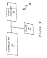
- FIG. 5 is a high-level block diagram of a flash memory device 10 of the present invention.
- Figure 5 is adapted from Figure 1 of US Patent No. 5,404,485 to Ban .
- Memory device 10 includes a flash memory 12 that is managed by a controller 14 with the help of a random access memory 16 as described in the Ban patent.
- Controller 14 stores multiple bits of data in each cell of flash memory 12 in accordance with the principles of the present invention.
- Appendix E 4-bits, 16 comparisons, almost equal spread for dy
Landscapes
- Engineering & Computer Science (AREA)
- Computer Hardware Design (AREA)
- Microelectronics & Electronic Packaging (AREA)
- Read Only Memory (AREA)
Claims (14)
- Verfahren zum Speichern von N Bits Daten in nichtflüchtigen Multi-Level-Speicherzellen, die jeweils zum Speichern von M Bits fähig sind, umfassend die folgenden Schritte:a) Vorsehen von [N/M] Zellen; und
gekennzeichnet durch:b) Programmieren jeder der Zellen mit bis zu M der Bits gemäß einer gültigen, nichtseriellen Bitreihenfolge, die ein Kriterium erfüllt, das aus der Gruppe ausgewählt ist, die besteht aus:i) eine maximale Anzahl von Schwellenspannungsvergleichen zum statischen Lesen eines der M Bits ist minimiert,ii) eine maximale Anzahl von Schwellenspannungsvergleichen zum statischen Lesen eines der M Bits übersteigt eine Mindestanzahl von Schwellenspannungsvergleichen zum statischen Lesen eines der M Bits um höchstens 1,iii) eine maximale Anzahl von Schwellenspannungsvergleichen zum dynamischen Lesen eines der M Bits ist minimiert, undiv) eine maximale Anzahl von Schwellenspannungsvergleichen zum dynamischen Lesen eines der M Bits übersteigt eine Mindestanzahl von Schwellenspannungsvergleichen zum dynamischen Lesen eines der M Bits um höchstens 1;
wobei M mindestens 3 beträgt,
wobei beim statischen Lesen alle Referenzspannungswerte, die während des Lesens verwendet werden, vor dem Start des Lesens vollständig vorbestimmt sind und beim dynamischen Lesen mindestens ein Referenzspannungswert, der während des Lesevorgangs verwendet wird, auf der Grundlage des Ergebnisses eines vorhergehenden Vergleichs, der während des gleichen Lesens durchgeführt wurde, bestimmt wird, und
wobei die Bitreihenfolge gültig ist, wenn ein niedrigstwertig programmierter Zustand einem Bitmuster mit lauter "1en" entspricht und jede Abfolge einer Bitprogrammierung nicht erfordern würde, dass eine Speicherzelle von einem höherwertig programmierten Zustand in einen niedrigerwertig programmierten Zustand übergeht. - Verfahren gemäß Anspruch 1, wobei M = 3 ist und wobei die Bitreihenfolge {7, 6, 4, 5, 1, 3, 2, 0} ist.
- Verfahren gemäß Anspruch 1, wobei M = 3 ist und wobei die Bitreihenfolge eine aus den Folgenden ist:{7, 6, 2, 3, 5, 4, 0, 1},{7, 6, 4, 0, 2, 3, 5, 1},{7, 6, 4, 0, 5, 1, 3, 2},{7, 6, 4, 5, 0, 2, 3, 1},{7, 6, 4, 5, 0, 1, 3, 2},{7, 6, 4, 5, 1, 0, 3, 2},{7, 6, 4, 5, 1, 3, 0, 2},{7, 6, 4, 5, 3, 1, 0, 2},{7, 6, 5, 4, 0, 2, 3, 1},{7, 6, 5, 4, 0, 1, 3, 2},{7, 5, 6, 4, 0, 2, 3, 1},{7, 5, 6, 4, 0, 1, 3, 2},{7, 5, 1, 3, 6, 4, 0, 2} und{7, 3, 6, 4, 5, 1, 0, 2}.
- Verfahren gemäß Anspruch 1, wobei das Kriterium darin besteht, dass die maximale Anzahl von Schwellenspannungsvergleichen zum statischen Lesen eines der M Bits minimiert ist.
- Verfahren gemäß Anspruch 1, wobei M = 3 ist und wobei die Bitreihenfolge eine aus den Folgenden ist:{7, 6, 2, 4, 5, 1, 3, 0},{7, 6, 2, 4, 5, 3, 1, 0},{7, 6, 4, 2, 3, 5, 1, 0},{7, 6, 4, 0, 2, 3, 5, 1},{7, 6, 4, 0, 5, 1, 3, 2},{7, 6, 4, 5, 1, 3, 2, 0},{7, 6, 5, 1, 3, 2, 4, 0},{7, 5, 6, 2, 3, 1, 4, 0},{7, 3, 6, 4, 5, 1, 2, 0} und{7, 3, 6, 4, 5, 1, 0, 2}.
- Verfahren gemäß Anspruch 1, wobei M = 3 ist und wobei die Bitreihenfolge eine aus den Folgenden ist:{7, 6, 2, 3, 4, 0, 5, 1},{7, 6, 2, 3, 4, 5, 0, 1},{7, 6, 2, 3, 4, 5, 1, 0},{7, 6, 2, 3, 5, 4, 0, 1},{7, 6, 2, 3, 5, 4, 1, 0},{7, 6, 2, 3, 5, 1, 4, 0},{7, 6, 4, 5, 2, 0, 1, 3},{7, 6, 4, 5, 2, 0, 3, 1},{7, 6, 4, 5, 2, 1, 0, 3},{7, 6, 4, 5, 2, 1, 3, 0},{7, 6, 4, 5, 2, 3, 0, 1},{7, 6, 4, 5, 2, 3, 1, 0},{7, 6, 4, 5, 0, 2, 1, 3},{7, 6, 4, 5, 0, 2, 3, 1},{7, 6, 4, 5, 0, 1, 2, 3},{7, 6, 4, 5, 0, 1, 3, 2},{7, 6, 4, 5, 0, 3, 1, 2},{7, 6, 4, 5, 0, 3, 2, 1},{7, 6, 4, 5, 1, 2, 0, 3},{7, 6, 4, 5, 1, 2, 3, 0},{7, 6, 4, 5, 1, 0, 3, 2},{7, 6, 4, 5, 1, 3, 2, 0},{7, 6, 4, 5, 1, 3, 0, 2},{7, 6, 4, 5, 3, 2, 1, 0},{7, 6, 4, 5, 3, 0, 2, 1},{7, 6, 4, 5, 3, 0, 1, 2},{7, 6, 4, 5, 3, 1, 2, 0},{7, 6, 4, 5, 3, 1, 0, 2},{7, 6, 5, 4, 2, 0, 1, 3},{7, 6, 5, 4, 2, 0, 3, 1},{7, 6, 5, 4, 2, 1, 0, 3},{7, 6, 5, 4, 2, 1, 3, 0},{7, 6, 5, 4, 2, 3, 0, 1},{7, 6, 5, 4, 2, 3, 1, 0},{7, 6, 5, 4, 0, 2, 1, 3},{7, 6, 5, 4, 0, 2, 3, 1},{7, 6, 5, 4, 0, 1, 2, 3},{7, 6, 5, 4, 0, 1, 3, 2},{7, 6, 5, 4, 0, 3, 1, 2},{7, 6, 5, 4, 0, 3, 2, 1},{7, 6, 5, 4, 1, 2, 0, 3},{7, 6, 5, 4, 1, 2, 3, 0},{7, 6, 5, 4, 1, 0, 2, 3},{7, 6, 5, 4, 1, 0, 3, 2},{7, 6, 5, 4, 1, 3, 2, 0},{7, 6, 5, 4, 1, 3, 0, 2},{7, 6, 5, 4, 3, 2, 0, 1},{7, 6, 5, 4, 3, 0, 2, 1},{7, 6, 5, 4, 3, 0, 1, 2},{7, 6, 5, 4, 3, 1, 2, 0},{7, 6, 5, 4, 3, 1, 0, 2},{7, 6, 3, 2, 4, 0, 5, 1},{7, 6, 3, 2, 4, 5, 0, 1},{7, 6, 3, 2, 4, 5, 1, 0},{7, 6, 3, 2, 5, 4, 0, 1},{7, 6, 3, 2, 5, 4, 1, 0},{7, 6, 3, 2, 5, 1, 4, 0},{7, 5, 6, 4, 2, 0, 1, 3},{7, 5, 6, 4, 2, 0, 3, 1},{7, 5, 6, 4, 2, 1, 0, 3},{7, 5, 6, 4, 2, 1, 3, 0},{7, 5, 6, 4, 2, 3, 0, 1},{7, 5, 6, 4, 2, 3, 1, 0},{7, 5, 6, 4, 0, 2, 1, 3},{7, 5, 6, 4, 0, 2, 3, 1},{7, 5, 6, 4, 0, 1, 2, 3},{7, 5, 6, 4, 0, 1, 3, 2},{7, 5, 6, 4, 0, 3, 1, 2},{7, 5, 6, 4, 0, 3, 2, 1},{7, 5, 6, 4, 1, 2, 0, 3},{7, 5, 6, 4, 1, 2, 3, 0},{7, 5, 6, 4, 1, 0, 2, 3},{7, 5, 6, 4, 1, 0, 3, 2},{7, 5, 6, 4, 1, 3, 2, 0},{7, 5, 8, 4, 1, 3, 0, 2},{7, 5, 6, 4, 3, 2, 0, 1},{7, 5, 6, 4, 3, 2, 1, 0},{7, 5, 6, 4, 3, 0, 2, 1},{7, 5, 6, 4, 3, 0, 1, 2},{7, 5, 6, 4, 3, 1, 2, 0},{7, 5, 6, 4, 3, 1, 0, 2},{7, 5, 1, 3, 6, 2, 4, 0},{7, 5, 1, 3, 6, 4, 2, 0},{7, 5, 1, 3, 6, 4, 0, 2},{7, 5, 3, 1, 6, 2, 4, 0},{7, 5, 3, 1, 6, 4, 2, 0},{7, 5, 3, 1, 6, 4, 0, 2},{7, 3, 6, 2, 4, 0, 5, 1},{7, 3, 6, 2, 4, 5, 0, 1},{7, 3, 6, 2, 4, 5, 1, 0},{7, 3, 6, 2, 5, 4, 0, 1},{7, 3, 6, 2, 5, 4, 1, 0},{7, 3, 6, 2, 5, 1, 4, 0},{7, 3, 5, 1, 6, 2, 4, 0},{7, 3, 5, 1, 6, 4, 2, 0} und{7, 3, 5,1, 6, 4, 0, 2}.
- Verfahren gemäß Anspruch 1, wobei das Kriterium darin besteht, dass die maximale Anzahl von Schwellenspannungsvergleichen zum statischen Lesen eines der M Bits die minimale Anzahl von Schwellenspannungsvergleichen zum statischen Lesen eines der M Bits um höchstens 1 übersteigt.
- Verfahren gemäß Anspruch 1, wobei M = 3 ist und wobei die Bitreihenfolge eine aus den Folgenden ist:{7, 6, 2, 4, 5, 1, 3, 0},{7, 6, 2, 4, 5, 3, 1, 0},{7, 6, 4, 2, 3, 5, 1, 0} und{7, 6, 5, 1, 3, 2, 4, 0}.
- Verfahren gemäß Anspruch 1, wobei M = 3 ist und wobei die Bitreihenfolge eine aus den Folgenden ist:{7, 6, 2, 4, 5, 0, 3, 1},{7, 6, 2, 4, 5, 3, 0, 1},{7, 6, 2, 5, 4, 0, 3, 1},{7, 6, 4, 2, 5, 0, 1, 3},{7, 6, 4, 2, 5, 1, 0, 3},{7, 6, 4, 2, 3, 0, 5, 1},{7, 6, 4, 2, 3, 5, 0, 1},{7, 6, 4, 0, 2, 3, 5, 1},{7, 6, 4, 0, 5, 2, 1, 3},{7, 6, 4, 0, 5, 2, 3, 1},{7, 6, 4, 0, 5, 1, 3, 2},{7, 6, 4, 0, 5, 3, 1, 2},{7, 6, 4, 0, 5, 3, 2, 1},{7. 6, 4, 0, 3, 2, 5, 1),{7, 6, 4, 0, 3, 5, 1, 2},{7, 6, 4, 3, 2, 0, 5, 1},{7, 6, 4, 3, 5,1, 0, 2},{7, 6, 5, 2, 4, 0, 1, 3},{7, 6, 5, 1, 2, 4, 0, 3},{7, 6, 5, 1, 4, 2, 0, 3},{7, 6, 5, 1, 3, 4, 0, 2}.{7, 6, 5, 3, 2, 4, 0, 1},{7, 6, 5, 3, 1, 4, 0, 2},{7, 6, 3, 5, 4, 2, 0, 1},{7, 6, 3, 5, 4, 0, 2, 1},{7, 5, 6, 2, 4, 1, 0, 3},{7, 5, 6, 2, 1, 4, 0, 3},{7, 5, 6, 2, 3, 4, 0, 1},7, 5, 6, 1, 4, 0, 2, 3},{7, 5, 6, 3, 2, 4, 0, 1},{7, 5, 6, 3, 1, 4, 0, 2},{7, 5, 1, 6, 4, 0, 3, 2},{7, 5, 3, 6, 4, 0, 1, 2},{7, 5, 3, 6, 4, 1, 0, 2},{7, 3, 6, 4, 5, 2, 0, 1},{7, 3, 6, 4, 5, 0, 2, 1},{7, 3, 6, 5, 4, 2, 0, 1},{7, 3, 6, 5, 4, 0, 2, 1},{7, 3, 5, 6, 4, 0, 1, 2} und{7, 3, 5, 6, 4, 1, 0, 2}.
- Speichervorrichtung (10), umfassend:a) einen Speicher (12), der K nichtflüchtige Multi-Level-Speicherzellen enthält, die jeweils zum Speichern von M Bits fähig sind; und gekennzeichnet durchb) einen Controller (14), der dazu betrieben wird, N Bits Daten in den Zellen zu speichern durch Programmieren jeder der Zellen mit bis zu M = [N/K] der Bits gemäß einer gültigen, nichtseriellen Bitreihenfolge, die ein Kriterium erfüllt, das aus der Gruppe ausgewählt ist, die besteht aus:i) eine maximale Anzahl von Schwellenspannungsvergleichen zum statischen Lesen eines der M Bits ist minimiert,ii) eine maximale Anzahl von Schwellenspannungsvergleichen zum statischen Lesen eines der M Bits übersteigt eine Mindestanzahl von Schwellenspannungsvergleichen zum statischen Lesen eines der M Bits um höchstens 1,iii) eine maximale Anzahl von Schwellenspannungsvergleichen zum dynamischen Lesen eines der M Bits ist minimiert, undiv) eine maximale Anzahl von Schwellenspannungsvergleichen zum dynamischen Lesen eines der M Bits übersteigt eine Mindestanzahl von Schwellenspannungsvergleichen zum dynamischen Lesen eines der M Bits um höchstens 1, wobei M mindestens 3 beträgt,
wobei beim statischen Lesen alle Referenzspannungswerte, die während des Lesens verwendet werden, vor dem Start des Lesens vollständig vorbestimmt sind und beim dynamischen Lesen mindestens ein Referenzspannungswert, der während des Lesevorgangs verwendet wird, auf der Grundlage des Ergebnisses eines vorhergehenden Vergleichs, der während des gleichen Lesens durchgeführt wurde, bestimmt wird, und
wobei die Bitreihenfolge gültig ist, wenn ein niedrigstwertig programmierter Zustand einem Bitmuster mit lauter "1en" entspricht und jede Abfolge einer Bitprogrammierung nicht erfordern würde, dass eine Speicherzelle von einem höherwertig programmierten Zustand in einen niedrigerwertig programmierten Zustand übergeht. - Speichervorrichtung gemäß Anspruch 10, wobei M = 3 ist und wobei die Bitreihenfolge {7, 6, 4, 5, 1, 3, 2, 0} ist.
- Speichervorrichtung gemäß Anspruch 10, wobei M = 3 ist und wobei die Bitreihenfolge eine aus den Folgenden ist:{7, 6, 2, 3, 5, 4, 0, 1},{7, 6, 4, 0, 2, 3, 5, 1},{7, 6, 4, 0, 5, 1, 3, 2},{7, 6, 4, 5, 0, 2, 3, 1},{7, 6, 4, 5, 0, 1, 3, 2},{7, 6, 4, 5,1, 0, 3, 2},{7, 6, 4, 5, 1, 3, 0, 2},{7, 6, 4, 5, 3, 1, 0, 2},{7, 6, 5, 4, 0, 2, 3, 1},{7, 6, 5, 4, 0, 1, 3, 2},{7, 5, 6, 4, 0, 2, 3, 1},{7, 5, 6, 4, 0, 1, 3, 2},{7, 5, 1, 3, 6, 4, 0, 2} und{7, 3, 6, 4, 5, 1, 0, 2}.
- Speichervorrichtung gemäß Anspruch 10, wobei das Kriterium darin besteht, dass die maximale Anzahl von Schwellenspannungsvergleichen zum statischen Lesen eines der M Bits minimiert ist.
- Speichervorrichtung gemäß Anspruch 10, wobei M = 3 ist und wobei die Bitreihenfolge eine aus den Folgenden ist:{7, 6, 2, 4, 5, 1, 3, 0},{7, 6, 2, 4, 5, 3, 1, 0},{7, 6, 4, 2, 3, 5, 1, 0},{7, 6, 4, 0, 2, 3, 5, 1},{7, 6, 4, 0, 5, 1, 3, 2},{7, 6, 4, 5,1, 3, 2, 0},{7, 6, 5, 1, 3, 2, 4, 0},{7, 5, 6, 2, 3, 1, 4, 0},{7, 3, 6, 4, 5, 1, 2, 0} und{7, 3, 6, 4, 5, 1, 0, 2}.
Applications Claiming Priority (3)
| Application Number | Priority Date | Filing Date | Title |
|---|---|---|---|
| US55379804P | 2004-03-14 | 2004-03-14 | |
| US11/035,807 US7310347B2 (en) | 2004-03-14 | 2005-01-18 | States encoding in multi-bit flash cells |
| PCT/IL2005/000251 WO2005086576A2 (en) | 2004-03-14 | 2005-03-03 | States encoding in multi-bit flash cells |
Publications (3)
| Publication Number | Publication Date |
|---|---|
| EP1735967A2 EP1735967A2 (de) | 2006-12-27 |
| EP1735967A4 EP1735967A4 (de) | 2011-03-16 |
| EP1735967B1 true EP1735967B1 (de) | 2014-06-25 |
Family
ID=34921941
Family Applications (1)
| Application Number | Title | Priority Date | Filing Date |
|---|---|---|---|
| EP05709145.6A Expired - Lifetime EP1735967B1 (de) | 2004-03-14 | 2005-03-03 | Zustandscodierung in mehrbit-flash-zellen |
Country Status (4)
| Country | Link |
|---|---|
| US (1) | US7310347B2 (de) |
| EP (1) | EP1735967B1 (de) |
| KR (1) | KR100931890B1 (de) |
| WO (1) | WO2005086576A2 (de) |
Families Citing this family (102)
| Publication number | Priority date | Publication date | Assignee | Title |
|---|---|---|---|---|
| US7716413B2 (en) * | 2004-02-15 | 2010-05-11 | Sandisk Il Ltd. | Method of making a multi-bit-cell flash memory |
| US8019928B2 (en) * | 2004-02-15 | 2011-09-13 | Sandisk Il Ltd. | Method of managing a multi-bit-cell flash memory |
| JP2006302345A (ja) * | 2005-04-15 | 2006-11-02 | Sony Corp | データ処理装置、データ再生装置、データ処理方法及びプログラム |
| US7526715B2 (en) * | 2005-10-17 | 2009-04-28 | Ramot At Tel Aviv University Ltd. | Probabilistic error correction in multi-bit-per-cell flash memory |
| CN103280239B (zh) * | 2006-05-12 | 2016-04-06 | 苹果公司 | 存储设备中的失真估计和消除 |
| US8239735B2 (en) | 2006-05-12 | 2012-08-07 | Apple Inc. | Memory Device with adaptive capacity |
| US8156403B2 (en) | 2006-05-12 | 2012-04-10 | Anobit Technologies Ltd. | Combined distortion estimation and error correction coding for memory devices |
| US8060806B2 (en) | 2006-08-27 | 2011-11-15 | Anobit Technologies Ltd. | Estimation of non-linear distortion in memory devices |
| US7975192B2 (en) * | 2006-10-30 | 2011-07-05 | Anobit Technologies Ltd. | Reading memory cells using multiple thresholds |
| US7924648B2 (en) * | 2006-11-28 | 2011-04-12 | Anobit Technologies Ltd. | Memory power and performance management |
| WO2008068747A2 (en) | 2006-12-03 | 2008-06-12 | Anobit Technologies Ltd. | Automatic defect management in memory devices |
| US7900102B2 (en) | 2006-12-17 | 2011-03-01 | Anobit Technologies Ltd. | High-speed programming of memory devices |
| US7751240B2 (en) | 2007-01-24 | 2010-07-06 | Anobit Technologies Ltd. | Memory device with negative thresholds |
| US8151166B2 (en) | 2007-01-24 | 2012-04-03 | Anobit Technologies Ltd. | Reduction of back pattern dependency effects in memory devices |
| WO2008111058A2 (en) | 2007-03-12 | 2008-09-18 | Anobit Technologies Ltd. | Adaptive estimation of memory cell read thresholds |
| US8001320B2 (en) | 2007-04-22 | 2011-08-16 | Anobit Technologies Ltd. | Command interface for memory devices |
| US8429493B2 (en) * | 2007-05-12 | 2013-04-23 | Apple Inc. | Memory device with internal signap processing unit |
| US8234545B2 (en) | 2007-05-12 | 2012-07-31 | Apple Inc. | Data storage with incremental redundancy |
| US7925936B1 (en) * | 2007-07-13 | 2011-04-12 | Anobit Technologies Ltd. | Memory device with non-uniform programming levels |
| US8259497B2 (en) | 2007-08-06 | 2012-09-04 | Apple Inc. | Programming schemes for multi-level analog memory cells |
| US8174905B2 (en) | 2007-09-19 | 2012-05-08 | Anobit Technologies Ltd. | Programming orders for reducing distortion in arrays of multi-level analog memory cells |
| US8068360B2 (en) | 2007-10-19 | 2011-11-29 | Anobit Technologies Ltd. | Reading analog memory cells using built-in multi-threshold commands |
| US8000141B1 (en) | 2007-10-19 | 2011-08-16 | Anobit Technologies Ltd. | Compensation for voltage drifts in analog memory cells |
| US8527819B2 (en) | 2007-10-19 | 2013-09-03 | Apple Inc. | Data storage in analog memory cell arrays having erase failures |
| KR101509836B1 (ko) | 2007-11-13 | 2015-04-06 | 애플 인크. | 멀티 유닛 메모리 디바이스에서의 메모리 유닛의 최적화된 선택 |
| US8225181B2 (en) | 2007-11-30 | 2012-07-17 | Apple Inc. | Efficient re-read operations from memory devices |
| US8209588B2 (en) | 2007-12-12 | 2012-06-26 | Anobit Technologies Ltd. | Efficient interference cancellation in analog memory cell arrays |
| US8085586B2 (en) | 2007-12-27 | 2011-12-27 | Anobit Technologies Ltd. | Wear level estimation in analog memory cells |
| US8301912B2 (en) | 2007-12-31 | 2012-10-30 | Sandisk Technologies Inc. | System, method and memory device providing data scrambling compatible with on-chip copy operation |
| US8156398B2 (en) | 2008-02-05 | 2012-04-10 | Anobit Technologies Ltd. | Parameter estimation based on error correction code parity check equations |
| US7924587B2 (en) | 2008-02-21 | 2011-04-12 | Anobit Technologies Ltd. | Programming of analog memory cells using a single programming pulse per state transition |
| US7864573B2 (en) * | 2008-02-24 | 2011-01-04 | Anobit Technologies Ltd. | Programming analog memory cells for reduced variance after retention |
| US8230300B2 (en) | 2008-03-07 | 2012-07-24 | Apple Inc. | Efficient readout from analog memory cells using data compression |
| US8400858B2 (en) | 2008-03-18 | 2013-03-19 | Apple Inc. | Memory device with reduced sense time readout |
| US8059457B2 (en) | 2008-03-18 | 2011-11-15 | Anobit Technologies Ltd. | Memory device with multiple-accuracy read commands |
| US8059455B2 (en) * | 2008-05-09 | 2011-11-15 | Sandisk Il Ltd. | Partial scrambling to reduce correlation |
| US8111548B2 (en) * | 2008-07-21 | 2012-02-07 | Sandisk Technologies Inc. | Programming non-volatile storage using binary and multi-state programming processes |
| US7924613B1 (en) | 2008-08-05 | 2011-04-12 | Anobit Technologies Ltd. | Data storage in analog memory cells with protection against programming interruption |
| US7995388B1 (en) | 2008-08-05 | 2011-08-09 | Anobit Technologies Ltd. | Data storage using modified voltages |
| US8949684B1 (en) | 2008-09-02 | 2015-02-03 | Apple Inc. | Segmented data storage |
| US8169825B1 (en) | 2008-09-02 | 2012-05-01 | Anobit Technologies Ltd. | Reliable data storage in analog memory cells subjected to long retention periods |
| US8000135B1 (en) | 2008-09-14 | 2011-08-16 | Anobit Technologies Ltd. | Estimation of memory cell read thresholds by sampling inside programming level distribution intervals |
| US8482978B1 (en) | 2008-09-14 | 2013-07-09 | Apple Inc. | Estimation of memory cell read thresholds by sampling inside programming level distribution intervals |
| US8239734B1 (en) | 2008-10-15 | 2012-08-07 | Apple Inc. | Efficient data storage in storage device arrays |
| US8261159B1 (en) | 2008-10-30 | 2012-09-04 | Apple, Inc. | Data scrambling schemes for memory devices |
| US8208304B2 (en) | 2008-11-16 | 2012-06-26 | Anobit Technologies Ltd. | Storage at M bits/cell density in N bits/cell analog memory cell devices, M>N |
| US8248831B2 (en) | 2008-12-31 | 2012-08-21 | Apple Inc. | Rejuvenation of analog memory cells |
| US8174857B1 (en) | 2008-12-31 | 2012-05-08 | Anobit Technologies Ltd. | Efficient readout schemes for analog memory cell devices using multiple read threshold sets |
| US8924661B1 (en) | 2009-01-18 | 2014-12-30 | Apple Inc. | Memory system including a controller and processors associated with memory devices |
| US8228701B2 (en) | 2009-03-01 | 2012-07-24 | Apple Inc. | Selective activation of programming schemes in analog memory cell arrays |
| KR20100106142A (ko) * | 2009-03-23 | 2010-10-01 | 삼성전자주식회사 | 불휘발성 메모리 장치 및 그것을 포함하는 메모리 시스템 |
| US8832354B2 (en) | 2009-03-25 | 2014-09-09 | Apple Inc. | Use of host system resources by memory controller |
| US8259506B1 (en) | 2009-03-25 | 2012-09-04 | Apple Inc. | Database of memory read thresholds |
| US8238157B1 (en) | 2009-04-12 | 2012-08-07 | Apple Inc. | Selective re-programming of analog memory cells |
| US8027195B2 (en) | 2009-06-05 | 2011-09-27 | SanDisk Technologies, Inc. | Folding data stored in binary format into multi-state format within non-volatile memory devices |
| US8102705B2 (en) | 2009-06-05 | 2012-01-24 | Sandisk Technologies Inc. | Structure and method for shuffling data within non-volatile memory devices |
| US20110002169A1 (en) | 2009-07-06 | 2011-01-06 | Yan Li | Bad Column Management with Bit Information in Non-Volatile Memory Systems |
| US8479080B1 (en) | 2009-07-12 | 2013-07-02 | Apple Inc. | Adaptive over-provisioning in memory systems |
| US8495465B1 (en) | 2009-10-15 | 2013-07-23 | Apple Inc. | Error correction coding over multiple memory pages |
| US8473809B2 (en) * | 2009-11-20 | 2013-06-25 | Sandisk Technologies Inc. | Data coding for improved ECC efficiency |
| US8677054B1 (en) | 2009-12-16 | 2014-03-18 | Apple Inc. | Memory management schemes for non-volatile memory devices |
| US8468294B2 (en) | 2009-12-18 | 2013-06-18 | Sandisk Technologies Inc. | Non-volatile memory with multi-gear control using on-chip folding of data |
| US20110153912A1 (en) | 2009-12-18 | 2011-06-23 | Sergey Anatolievich Gorobets | Maintaining Updates of Multi-Level Non-Volatile Memory in Binary Non-Volatile Memory |
| US8144512B2 (en) | 2009-12-18 | 2012-03-27 | Sandisk Technologies Inc. | Data transfer flows for on-chip folding |
| US8725935B2 (en) | 2009-12-18 | 2014-05-13 | Sandisk Technologies Inc. | Balanced performance for on-chip folding of non-volatile memories |
| US8694814B1 (en) | 2010-01-10 | 2014-04-08 | Apple Inc. | Reuse of host hibernation storage space by memory controller |
| US8572311B1 (en) | 2010-01-11 | 2013-10-29 | Apple Inc. | Redundant data storage in multi-die memory systems |
| US8694853B1 (en) | 2010-05-04 | 2014-04-08 | Apple Inc. | Read commands for reading interfering memory cells |
| US8572423B1 (en) | 2010-06-22 | 2013-10-29 | Apple Inc. | Reducing peak current in memory systems |
| US8417876B2 (en) | 2010-06-23 | 2013-04-09 | Sandisk Technologies Inc. | Use of guard bands and phased maintenance operations to avoid exceeding maximum latency requirements in non-volatile memory systems |
| US8595591B1 (en) | 2010-07-11 | 2013-11-26 | Apple Inc. | Interference-aware assignment of programming levels in analog memory cells |
| WO2012009318A1 (en) | 2010-07-13 | 2012-01-19 | Sandisk Technologies Inc. | Dynamic optimization of back-end memory system interface |
| US9104580B1 (en) | 2010-07-27 | 2015-08-11 | Apple Inc. | Cache memory for hybrid disk drives |
| US8645794B1 (en) | 2010-07-31 | 2014-02-04 | Apple Inc. | Data storage in analog memory cells using a non-integer number of bits per cell |
| US8856475B1 (en) | 2010-08-01 | 2014-10-07 | Apple Inc. | Efficient selection of memory blocks for compaction |
| US8694854B1 (en) | 2010-08-17 | 2014-04-08 | Apple Inc. | Read threshold setting based on soft readout statistics |
| US9021181B1 (en) | 2010-09-27 | 2015-04-28 | Apple Inc. | Memory management for unifying memory cell conditions by using maximum time intervals |
| US9342446B2 (en) | 2011-03-29 | 2016-05-17 | SanDisk Technologies, Inc. | Non-volatile memory system allowing reverse eviction of data updates to non-volatile binary cache |
| KR101818443B1 (ko) | 2011-07-08 | 2018-01-16 | 삼성전자주식회사 | 메모리 컨트롤러, 및 상기 메모리 컨트롤러를 포함하는 메모리 시스템 |
| US8775901B2 (en) | 2011-07-28 | 2014-07-08 | SanDisk Technologies, Inc. | Data recovery for defective word lines during programming of non-volatile memory arrays |
| KR20130041603A (ko) * | 2011-10-17 | 2013-04-25 | 삼성전자주식회사 | 비휘발성 메모리 장치의 데이터 저장 방법 |
| US8842473B2 (en) | 2012-03-15 | 2014-09-23 | Sandisk Technologies Inc. | Techniques for accessing column selecting shift register with skipped entries in non-volatile memories |
| US8681548B2 (en) | 2012-05-03 | 2014-03-25 | Sandisk Technologies Inc. | Column redundancy circuitry for non-volatile memory |
| US9076506B2 (en) | 2012-09-28 | 2015-07-07 | Sandisk Technologies Inc. | Variable rate parallel to serial shift register |
| US9490035B2 (en) | 2012-09-28 | 2016-11-08 | SanDisk Technologies, Inc. | Centralized variable rate serializer and deserializer for bad column management |
| US8897080B2 (en) | 2012-09-28 | 2014-11-25 | Sandisk Technologies Inc. | Variable rate serial to parallel shift register |
| US9361167B2 (en) | 2012-10-24 | 2016-06-07 | SanDisk Technologies, Inc. | Bit error rate estimation for wear leveling and for block selection based on data type |
| US9026757B2 (en) | 2013-01-25 | 2015-05-05 | Sandisk Technologies Inc. | Non-volatile memory programming data preservation |
| US8913428B2 (en) | 2013-01-25 | 2014-12-16 | Sandisk Technologies Inc. | Programming non-volatile storage system with multiple memory die |
| US9117530B2 (en) | 2013-03-14 | 2015-08-25 | Sandisk Technologies Inc. | Preserving data from adjacent word lines while programming binary non-volatile storage elements |
| US9009568B2 (en) | 2013-08-09 | 2015-04-14 | Sandisk Technologies Inc. | Sensing parameter management in non-volatile memory storage system to compensate for broken word lines |
| US9384128B2 (en) | 2014-04-18 | 2016-07-05 | SanDisk Technologies, Inc. | Multi-level redundancy code for non-volatile memory controller |
| US9934872B2 (en) | 2014-10-30 | 2018-04-03 | Sandisk Technologies Llc | Erase stress and delta erase loop count methods for various fail modes in non-volatile memory |
| US9224502B1 (en) | 2015-01-14 | 2015-12-29 | Sandisk Technologies Inc. | Techniques for detection and treating memory hole to local interconnect marginality defects |
| US10032524B2 (en) | 2015-02-09 | 2018-07-24 | Sandisk Technologies Llc | Techniques for determining local interconnect defects |
| US9269446B1 (en) | 2015-04-08 | 2016-02-23 | Sandisk Technologies Inc. | Methods to improve programming of slow cells |
| US9564219B2 (en) | 2015-04-08 | 2017-02-07 | Sandisk Technologies Llc | Current based detection and recording of memory hole-interconnect spacing defects |
| US9548107B1 (en) | 2015-07-09 | 2017-01-17 | Kabushiki Kaisha Toshiba | Semiconductor memory device |
| KR102451154B1 (ko) | 2015-12-07 | 2022-10-06 | 삼성전자주식회사 | 불휘발성 메모리 장치 및 불휘발성 메모리 장치의 동작 방법 |
| JP2020155185A (ja) * | 2019-03-22 | 2020-09-24 | キオクシア株式会社 | 半導体記憶装置 |
| US11556416B2 (en) | 2021-05-05 | 2023-01-17 | Apple Inc. | Controlling memory readout reliability and throughput by adjusting distance between read thresholds |
| US11847342B2 (en) | 2021-07-28 | 2023-12-19 | Apple Inc. | Efficient transfer of hard data and confidence levels in reading a nonvolatile memory |
Family Cites Families (11)
| Publication number | Priority date | Publication date | Assignee | Title |
|---|---|---|---|---|
| US5268870A (en) | 1988-06-08 | 1993-12-07 | Eliyahou Harari | Flash EEPROM system and intelligent programming and erasing methods therefor |
| US5404485A (en) | 1993-03-08 | 1995-04-04 | M-Systems Flash Disk Pioneers Ltd. | Flash file system |
| WO1997032253A1 (fr) * | 1996-02-29 | 1997-09-04 | Hitachi, Ltd. | Dispositif de memoire a semi-conducteur presentant des cellules defaillantes |
| US5903495A (en) | 1996-03-18 | 1999-05-11 | Kabushiki Kaisha Toshiba | Semiconductor device and memory system |
| US5909449A (en) | 1997-09-08 | 1999-06-01 | Invox Technology | Multibit-per-cell non-volatile memory with error detection and correction |
| US6314026B1 (en) * | 1999-02-08 | 2001-11-06 | Kabushiki Kaisha Toshiba | Nonvolatile semiconductor device using local self boost technique |
| JP4023953B2 (ja) | 1999-06-22 | 2007-12-19 | 株式会社ルネサステクノロジ | 不揮発性半導体記憶装置 |
| JP3631463B2 (ja) | 2001-12-27 | 2005-03-23 | 株式会社東芝 | 不揮発性半導体記憶装置 |
| US6493266B1 (en) * | 2001-04-09 | 2002-12-10 | Advanced Micro Devices, Inc. | Soft program and soft program verify of the core cells in flash memory array |
| US6522580B2 (en) | 2001-06-27 | 2003-02-18 | Sandisk Corporation | Operating techniques for reducing effects of coupling between storage elements of a non-volatile memory operated in multiple data states |
| US6847550B2 (en) * | 2002-10-25 | 2005-01-25 | Nexflash Technologies, Inc. | Nonvolatile semiconductor memory having three-level memory cells and program and read mapping circuits therefor |
-
2005
- 2005-01-18 US US11/035,807 patent/US7310347B2/en active Active
- 2005-03-03 EP EP05709145.6A patent/EP1735967B1/de not_active Expired - Lifetime
- 2005-03-03 WO PCT/IL2005/000251 patent/WO2005086576A2/en not_active Ceased
- 2005-03-03 KR KR1020067021322A patent/KR100931890B1/ko not_active Expired - Fee Related
Also Published As
| Publication number | Publication date |
|---|---|
| EP1735967A4 (de) | 2011-03-16 |
| WO2005086576A2 (en) | 2005-09-22 |
| US20050201401A1 (en) | 2005-09-15 |
| KR100931890B1 (ko) | 2009-12-15 |
| US7310347B2 (en) | 2007-12-18 |
| EP1735967A2 (de) | 2006-12-27 |
| KR20070010150A (ko) | 2007-01-22 |
| WO2005086576A3 (en) | 2008-10-16 |
Similar Documents
| Publication | Publication Date | Title |
|---|---|---|
| EP1735967B1 (de) | Zustandscodierung in mehrbit-flash-zellen | |
| US8055972B2 (en) | States encoding in multi-bit flash cells for optimizing error rate | |
| US7493457B2 (en) | States encoding in multi-bit flash cells for optimizing error rate | |
| US7558115B2 (en) | Program method of flash memory device | |
| US7716413B2 (en) | Method of making a multi-bit-cell flash memory | |
| KR100922515B1 (ko) | 플래시 메모리의 신뢰성을 높이는 방법 | |
| US7548457B2 (en) | Multi-bit nonvolatile memory device and related programming method | |
| US8159882B2 (en) | Nonvolatile semiconductor memory device and memory system | |
| US7855913B2 (en) | Dynamically configurable MLC state assignment | |
| US20100135077A1 (en) | Method of performing read operation in flash memory device | |
| US7839678B2 (en) | NAND type flash memory and write method of the same | |
| US7623375B2 (en) | Method of operating a flash memory device | |
| US8050103B2 (en) | Method of programming nonvolatile memory device | |
| US7274599B2 (en) | NOR flash memory device using bit scan method and related programming method | |
| KR20090011207A (ko) | 3비트 멀티 레벨 셀 메모리 소자의 프로그램 방법 | |
| KR100719381B1 (ko) | 어드레스 설정 플래그를 갖는 멀티 레벨 셀 낸드형 플래시메모리 | |
| KR100261021B1 (ko) | 반도체 메모리 장치의 소거 방법 |
Legal Events
| Date | Code | Title | Description |
|---|---|---|---|
| PUAI | Public reference made under article 153(3) epc to a published international application that has entered the european phase |
Free format text: ORIGINAL CODE: 0009012 |
|
| 17P | Request for examination filed |
Effective date: 20061006 |
|
| AK | Designated contracting states |
Kind code of ref document: A2 Designated state(s): AT BE BG CH CY CZ DE DK EE ES FI FR GB GR HU IE IS IT LI LT LU MC NL PL PT RO SE SI SK TR |
|
| AX | Request for extension of the european patent |
Extension state: AL BA HR LV MK YU |
|
| DAX | Request for extension of the european patent (deleted) | ||
| PUAK | Availability of information related to the publication of the international search report |
Free format text: ORIGINAL CODE: 0009015 |
|
| RIC1 | Information provided on ipc code assigned before grant |
Ipc: H04L 12/28 20060101AFI20081029BHEP |
|
| RAP1 | Party data changed (applicant data changed or rights of an application transferred) |
Owner name: SANDISK IL LTD. |
|
| A4 | Supplementary search report drawn up and despatched |
Effective date: 20110214 |
|
| RIC1 | Information provided on ipc code assigned before grant |
Ipc: G11C 16/10 20060101ALI20110208BHEP Ipc: G11C 11/56 20060101ALI20110208BHEP Ipc: H04L 12/28 20060101AFI20081029BHEP |
|
| 17Q | First examination report despatched |
Effective date: 20110728 |
|
| REG | Reference to a national code |
Ref country code: DE Ref legal event code: R079 Ref document number: 602005044000 Country of ref document: DE Free format text: PREVIOUS MAIN CLASS: H04L0012560000 Ipc: G11C0007100000 |
|
| RIC1 | Information provided on ipc code assigned before grant |
Ipc: G11C 11/56 20060101ALI20131121BHEP Ipc: G11C 16/10 20060101ALI20131121BHEP Ipc: G11C 7/10 20060101AFI20131121BHEP |
|
| GRAP | Despatch of communication of intention to grant a patent |
Free format text: ORIGINAL CODE: EPIDOSNIGR1 |
|
| INTG | Intention to grant announced |
Effective date: 20140124 |
|
| GRAS | Grant fee paid |
Free format text: ORIGINAL CODE: EPIDOSNIGR3 |
|
| GRAA | (expected) grant |
Free format text: ORIGINAL CODE: 0009210 |
|
| AK | Designated contracting states |
Kind code of ref document: B1 Designated state(s): AT BE BG CH CY CZ DE DK EE ES FI FR GB GR HU IE IS IT LI LT LU MC NL PL PT RO SE SI SK TR |
|
| REG | Reference to a national code |
Ref country code: GB Ref legal event code: FG4D |
|
| REG | Reference to a national code |
Ref country code: CH Ref legal event code: EP |
|
| REG | Reference to a national code |
Ref country code: AT Ref legal event code: REF Ref document number: 675119 Country of ref document: AT Kind code of ref document: T Effective date: 20140715 |
|
| REG | Reference to a national code |
Ref country code: IE Ref legal event code: FG4D |
|
| REG | Reference to a national code |
Ref country code: DE Ref legal event code: R096 Ref document number: 602005044000 Country of ref document: DE Effective date: 20140731 |
|
| PG25 | Lapsed in a contracting state [announced via postgrant information from national office to epo] |
Ref country code: LT Free format text: LAPSE BECAUSE OF FAILURE TO SUBMIT A TRANSLATION OF THE DESCRIPTION OR TO PAY THE FEE WITHIN THE PRESCRIBED TIME-LIMIT Effective date: 20140625 Ref country code: CY Free format text: LAPSE BECAUSE OF FAILURE TO SUBMIT A TRANSLATION OF THE DESCRIPTION OR TO PAY THE FEE WITHIN THE PRESCRIBED TIME-LIMIT Effective date: 20140625 Ref country code: GR Free format text: LAPSE BECAUSE OF FAILURE TO SUBMIT A TRANSLATION OF THE DESCRIPTION OR TO PAY THE FEE WITHIN THE PRESCRIBED TIME-LIMIT Effective date: 20140926 Ref country code: FI Free format text: LAPSE BECAUSE OF FAILURE TO SUBMIT A TRANSLATION OF THE DESCRIPTION OR TO PAY THE FEE WITHIN THE PRESCRIBED TIME-LIMIT Effective date: 20140625 |
|
| REG | Reference to a national code |
Ref country code: AT Ref legal event code: MK05 Ref document number: 675119 Country of ref document: AT Kind code of ref document: T Effective date: 20140625 |
|
| REG | Reference to a national code |
Ref country code: NL Ref legal event code: VDEP Effective date: 20140625 |
|
| REG | Reference to a national code |
Ref country code: LT Ref legal event code: MG4D |
|
| PG25 | Lapsed in a contracting state [announced via postgrant information from national office to epo] |
Ref country code: SE Free format text: LAPSE BECAUSE OF FAILURE TO SUBMIT A TRANSLATION OF THE DESCRIPTION OR TO PAY THE FEE WITHIN THE PRESCRIBED TIME-LIMIT Effective date: 20140625 |
|
| PG25 | Lapsed in a contracting state [announced via postgrant information from national office to epo] |
Ref country code: EE Free format text: LAPSE BECAUSE OF FAILURE TO SUBMIT A TRANSLATION OF THE DESCRIPTION OR TO PAY THE FEE WITHIN THE PRESCRIBED TIME-LIMIT Effective date: 20140625 Ref country code: PT Free format text: LAPSE BECAUSE OF FAILURE TO SUBMIT A TRANSLATION OF THE DESCRIPTION OR TO PAY THE FEE WITHIN THE PRESCRIBED TIME-LIMIT Effective date: 20141027 Ref country code: RO Free format text: LAPSE BECAUSE OF FAILURE TO SUBMIT A TRANSLATION OF THE DESCRIPTION OR TO PAY THE FEE WITHIN THE PRESCRIBED TIME-LIMIT Effective date: 20140625 Ref country code: SK Free format text: LAPSE BECAUSE OF FAILURE TO SUBMIT A TRANSLATION OF THE DESCRIPTION OR TO PAY THE FEE WITHIN THE PRESCRIBED TIME-LIMIT Effective date: 20140625 Ref country code: ES Free format text: LAPSE BECAUSE OF FAILURE TO SUBMIT A TRANSLATION OF THE DESCRIPTION OR TO PAY THE FEE WITHIN THE PRESCRIBED TIME-LIMIT Effective date: 20140625 Ref country code: CZ Free format text: LAPSE BECAUSE OF FAILURE TO SUBMIT A TRANSLATION OF THE DESCRIPTION OR TO PAY THE FEE WITHIN THE PRESCRIBED TIME-LIMIT Effective date: 20140625 |
|
| PG25 | Lapsed in a contracting state [announced via postgrant information from national office to epo] |
Ref country code: IS Free format text: LAPSE BECAUSE OF FAILURE TO SUBMIT A TRANSLATION OF THE DESCRIPTION OR TO PAY THE FEE WITHIN THE PRESCRIBED TIME-LIMIT Effective date: 20141025 Ref country code: NL Free format text: LAPSE BECAUSE OF FAILURE TO SUBMIT A TRANSLATION OF THE DESCRIPTION OR TO PAY THE FEE WITHIN THE PRESCRIBED TIME-LIMIT Effective date: 20140625 Ref country code: AT Free format text: LAPSE BECAUSE OF FAILURE TO SUBMIT A TRANSLATION OF THE DESCRIPTION OR TO PAY THE FEE WITHIN THE PRESCRIBED TIME-LIMIT Effective date: 20140625 Ref country code: PL Free format text: LAPSE BECAUSE OF FAILURE TO SUBMIT A TRANSLATION OF THE DESCRIPTION OR TO PAY THE FEE WITHIN THE PRESCRIBED TIME-LIMIT Effective date: 20140625 |
|
| REG | Reference to a national code |
Ref country code: DE Ref legal event code: R097 Ref document number: 602005044000 Country of ref document: DE |
|
| PG25 | Lapsed in a contracting state [announced via postgrant information from national office to epo] |
Ref country code: IT Free format text: LAPSE BECAUSE OF FAILURE TO SUBMIT A TRANSLATION OF THE DESCRIPTION OR TO PAY THE FEE WITHIN THE PRESCRIBED TIME-LIMIT Effective date: 20140625 Ref country code: DK Free format text: LAPSE BECAUSE OF FAILURE TO SUBMIT A TRANSLATION OF THE DESCRIPTION OR TO PAY THE FEE WITHIN THE PRESCRIBED TIME-LIMIT Effective date: 20140625 |
|
| PLBE | No opposition filed within time limit |
Free format text: ORIGINAL CODE: 0009261 |
|
| STAA | Information on the status of an ep patent application or granted ep patent |
Free format text: STATUS: NO OPPOSITION FILED WITHIN TIME LIMIT |
|
| 26N | No opposition filed |
Effective date: 20150326 |
|
| PG25 | Lapsed in a contracting state [announced via postgrant information from national office to epo] |
Ref country code: BE Free format text: LAPSE BECAUSE OF FAILURE TO SUBMIT A TRANSLATION OF THE DESCRIPTION OR TO PAY THE FEE WITHIN THE PRESCRIBED TIME-LIMIT Effective date: 20140625 |
|
| PG25 | Lapsed in a contracting state [announced via postgrant information from national office to epo] |
Ref country code: LU Free format text: LAPSE BECAUSE OF FAILURE TO SUBMIT A TRANSLATION OF THE DESCRIPTION OR TO PAY THE FEE WITHIN THE PRESCRIBED TIME-LIMIT Effective date: 20150303 Ref country code: MC Free format text: LAPSE BECAUSE OF FAILURE TO SUBMIT A TRANSLATION OF THE DESCRIPTION OR TO PAY THE FEE WITHIN THE PRESCRIBED TIME-LIMIT Effective date: 20140625 |
|
| REG | Reference to a national code |
Ref country code: CH Ref legal event code: PL |
|
| PG25 | Lapsed in a contracting state [announced via postgrant information from national office to epo] |
Ref country code: SI Free format text: LAPSE BECAUSE OF FAILURE TO SUBMIT A TRANSLATION OF THE DESCRIPTION OR TO PAY THE FEE WITHIN THE PRESCRIBED TIME-LIMIT Effective date: 20140625 |
|
| REG | Reference to a national code |
Ref country code: FR Ref legal event code: ST Effective date: 20151130 |
|
| REG | Reference to a national code |
Ref country code: IE Ref legal event code: MM4A |
|
| PG25 | Lapsed in a contracting state [announced via postgrant information from national office to epo] |
Ref country code: LI Free format text: LAPSE BECAUSE OF NON-PAYMENT OF DUE FEES Effective date: 20150331 Ref country code: IE Free format text: LAPSE BECAUSE OF NON-PAYMENT OF DUE FEES Effective date: 20150303 Ref country code: CH Free format text: LAPSE BECAUSE OF NON-PAYMENT OF DUE FEES Effective date: 20150331 |
|
| PG25 | Lapsed in a contracting state [announced via postgrant information from national office to epo] |
Ref country code: FR Free format text: LAPSE BECAUSE OF NON-PAYMENT OF DUE FEES Effective date: 20150331 |
|
| PG25 | Lapsed in a contracting state [announced via postgrant information from national office to epo] |
Ref country code: BG Free format text: LAPSE BECAUSE OF FAILURE TO SUBMIT A TRANSLATION OF THE DESCRIPTION OR TO PAY THE FEE WITHIN THE PRESCRIBED TIME-LIMIT Effective date: 20140625 Ref country code: HU Free format text: LAPSE BECAUSE OF FAILURE TO SUBMIT A TRANSLATION OF THE DESCRIPTION OR TO PAY THE FEE WITHIN THE PRESCRIBED TIME-LIMIT; INVALID AB INITIO Effective date: 20050303 |
|
| PG25 | Lapsed in a contracting state [announced via postgrant information from national office to epo] |
Ref country code: TR Free format text: LAPSE BECAUSE OF FAILURE TO SUBMIT A TRANSLATION OF THE DESCRIPTION OR TO PAY THE FEE WITHIN THE PRESCRIBED TIME-LIMIT Effective date: 20140625 |
|
| PGFP | Annual fee paid to national office [announced via postgrant information from national office to epo] |
Ref country code: GB Payment date: 20180228 Year of fee payment: 14 |
|
| PGFP | Annual fee paid to national office [announced via postgrant information from national office to epo] |
Ref country code: DE Payment date: 20190219 Year of fee payment: 15 |
|
| GBPC | Gb: european patent ceased through non-payment of renewal fee |
Effective date: 20190303 |
|
| PG25 | Lapsed in a contracting state [announced via postgrant information from national office to epo] |
Ref country code: GB Free format text: LAPSE BECAUSE OF NON-PAYMENT OF DUE FEES Effective date: 20190303 |
|
| REG | Reference to a national code |
Ref country code: DE Ref legal event code: R119 Ref document number: 602005044000 Country of ref document: DE |
|
| PG25 | Lapsed in a contracting state [announced via postgrant information from national office to epo] |
Ref country code: DE Free format text: LAPSE BECAUSE OF NON-PAYMENT OF DUE FEES Effective date: 20201001 |