EP1731966A1 - Exposure equipment - Google Patents
Exposure equipment Download PDFInfo
- Publication number
- EP1731966A1 EP1731966A1 EP05727502A EP05727502A EP1731966A1 EP 1731966 A1 EP1731966 A1 EP 1731966A1 EP 05727502 A EP05727502 A EP 05727502A EP 05727502 A EP05727502 A EP 05727502A EP 1731966 A1 EP1731966 A1 EP 1731966A1
- Authority
- EP
- European Patent Office
- Prior art keywords
- substrate
- exposure
- cooling
- spindle
- exposure device
- Prior art date
- Legal status (The legal status is an assumption and is not a legal conclusion. Google has not performed a legal analysis and makes no representation as to the accuracy of the status listed.)
- Withdrawn
Links
Images







Classifications
-
- F—MECHANICAL ENGINEERING; LIGHTING; HEATING; WEAPONS; BLASTING
- F16—ENGINEERING ELEMENTS AND UNITS; GENERAL MEASURES FOR PRODUCING AND MAINTAINING EFFECTIVE FUNCTIONING OF MACHINES OR INSTALLATIONS; THERMAL INSULATION IN GENERAL
- F16C—SHAFTS; FLEXIBLE SHAFTS; ELEMENTS OR CRANKSHAFT MECHANISMS; ROTARY BODIES OTHER THAN GEARING ELEMENTS; BEARINGS
- F16C37/00—Cooling of bearings
-
- B—PERFORMING OPERATIONS; TRANSPORTING
- B82—NANOTECHNOLOGY
- B82Y—SPECIFIC USES OR APPLICATIONS OF NANOSTRUCTURES; MEASUREMENT OR ANALYSIS OF NANOSTRUCTURES; MANUFACTURE OR TREATMENT OF NANOSTRUCTURES
- B82Y10/00—Nanotechnology for information processing, storage or transmission, e.g. quantum computing or single electron logic
-
- B—PERFORMING OPERATIONS; TRANSPORTING
- B82—NANOTECHNOLOGY
- B82Y—SPECIFIC USES OR APPLICATIONS OF NANOSTRUCTURES; MEASUREMENT OR ANALYSIS OF NANOSTRUCTURES; MANUFACTURE OR TREATMENT OF NANOSTRUCTURES
- B82Y40/00—Manufacture or treatment of nanostructures
-
- G—PHYSICS
- G03—PHOTOGRAPHY; CINEMATOGRAPHY; ANALOGOUS TECHNIQUES USING WAVES OTHER THAN OPTICAL WAVES; ELECTROGRAPHY; HOLOGRAPHY
- G03F—PHOTOMECHANICAL PRODUCTION OF TEXTURED OR PATTERNED SURFACES, e.g. FOR PRINTING, FOR PROCESSING OF SEMICONDUCTOR DEVICES; MATERIALS THEREFOR; ORIGINALS THEREFOR; APPARATUS SPECIALLY ADAPTED THEREFOR
- G03F7/00—Photomechanical, e.g. photolithographic, production of textured or patterned surfaces, e.g. printing surfaces; Materials therefor, e.g. comprising photoresists; Apparatus specially adapted therefor
- G03F7/70—Microphotolithographic exposure; Apparatus therefor
- G03F7/708—Construction of apparatus, e.g. environment aspects, hygiene aspects or materials
- G03F7/70858—Environment aspects, e.g. pressure of beam-path gas, temperature
- G03F7/70866—Environment aspects, e.g. pressure of beam-path gas, temperature of mask or workpiece
- G03F7/70875—Temperature, e.g. temperature control of masks or workpieces via control of stage temperature
-
- G—PHYSICS
- G11—INFORMATION STORAGE
- G11B—INFORMATION STORAGE BASED ON RELATIVE MOVEMENT BETWEEN RECORD CARRIER AND TRANSDUCER
- G11B7/00—Recording or reproducing by optical means, e.g. recording using a thermal beam of optical radiation by modifying optical properties or the physical structure, reproducing using an optical beam at lower power by sensing optical properties; Record carriers therefor
- G11B7/24—Record carriers characterised by shape, structure or physical properties, or by the selection of the material
- G11B7/26—Apparatus or processes specially adapted for the manufacture of record carriers
- G11B7/261—Preparing a master, e.g. exposing photoresist, electroforming
-
- H—ELECTRICITY
- H01—ELECTRIC ELEMENTS
- H01J—ELECTRIC DISCHARGE TUBES OR DISCHARGE LAMPS
- H01J37/00—Discharge tubes with provision for introducing objects or material to be exposed to the discharge, e.g. for the purpose of examination or processing thereof
- H01J37/30—Electron-beam or ion-beam tubes for localised treatment of objects
- H01J37/317—Electron-beam or ion-beam tubes for localised treatment of objects for changing properties of the objects or for applying thin layers thereon, e.g. for ion implantation
- H01J37/3174—Particle-beam lithography, e.g. electron beam lithography
Definitions
- the present invention relates to an exposure device, and particularly to an exposure device for carrying out exposure while moving the irradiation position of an exposure beam onto a substrate on which a resist is formed.
- a method using a chemical amplification type resist having high sensitivity and high resolution is used is known as a method of forming a fine pattern.
- the patterning method exposure (drawing) using an electron beam, post-exposure bake (PEB: Post Exposure Bake) and development are carried out on a substrate coated with a chemical amplification resist.
- PEB Post Exposure Bake
- a predetermined time is needed from the drawing step till the PEB step, and the size of a pattern achieved after the development is varied between a portion drawn at the initial stage of drawing and a portion drawn at the last stage on the same substrate.
- a method of solving the problem are disclosed a method of controlling the PEB condition on the basis of the time from the drawing step to the PEB step and the standby time characteristic of the resist (see, Japanese Laid-Open Patent Application Kokai No.08-111370 ) and a method of cooling the substrate to suppress the reaction during the period after the drawing step till the development step (see, Japanese Laid-Open Patent Application Kokai No.10-172882 ).
- the electron beam is irradiated to the drawing substrate with energy of several KeV to 100kev, for example.
- the resolution of the electron beam is dependent on the energy of the electron beam, and a high-energy electron beam is used when high resolution is achieved.
- a part of the energy of the electron beam is used for the exposure reaction of the resist.
- most of the other energy is converted to heat by scattering in the substrate, and the substrate is locally heated. Therefore, the reaction during the standby time is promoted by the heat.
- the related art described above has a problem that PED cannot be sufficiently controlled. Furthermore, the method of adjusting the PEB condition or the like has a drawback that the adjusting method and the adjusting condition are complicated and bothersome.
- the present invention has been made in view of the foregoing problems, and has an object to provide an inexpensive exposure device that can suppress PED (Post Exposure Delay) and achieve an excellently uniform pattern.
- PED Post Exposure Delay
- an exposure device for irradiating an exposure beam to a substrate having a resist formed thereon to form a latent image on the resist is characterized by comprising a substrate holder for holding the substrate, a driving portion for relatively changing the irradiation position of the exposure beam to the substrate, and a cooling portion for cooling the substrate during the irradiation of the exposure beam.
- an exposure device for irradiating an exposure beam to a substrate having a resist formed thereon to form a latent image is characterized by comprising a substrate holding portion for holding the substrate; a spindle for rotating the substrate holding portion; a fluid bearing portion for holding the spindle; and a conduit pipe that passes through the fluid bearing portion and the spindle to supply cooling fluid to the substrate holding portion.
- an exposure device for irradiating an exposure beam to a disc-shaped substrate having a resist formed thereon to form a latent image on the resist is characterized by comprising a substrate holding portion for holding the substrate and rotating the substrate, an irradiation portion for irradiating the exposure beam to the substrate; and a low temperature member that is disposed above the substrate and at the rotational downstream side of the irradiation position of the exposure beam.
- Fig. 1 is a block diagram showing the configuration of an electron beam exposure device 10 according to a first embodiment of the present invention.
- the electron beam exposure device 10 is a mastering device for creating a master disc such as a magnetic disc or an optical disc by using an electron beam.
- the electron beam exposure device 10 is equipped with a vacuum chamber 11, an electron beam column 12 secured to the vacuum chamber 11, driving devices 13, 14 for rotating and translating a substrate disposed in the vacuum chamber 11, various kinds of circuits for controlling the driving of the substrate, controlling the electron beam, etc., and a control system (not shown).
- the substrate 15 for the disc master is mounted on a turntable 16.
- the turntable 16 is provided on a rotating and feeding stage (hereinafter, simply referred to as stage) 17.
- stage 17 has a spindle motor 13 for rotating the turntable 16 on which the substrate 15 is mounted.
- the stage 17 is coupled to a feeding motor 14 for translating the turntable 16. Accordingly, the substrate 15 can be moved in a predetermined direction in a plane parallel to the principal surface of the substrate 15 while rotating the substrate 15.
- the turntable 16 may be equipped with an electrostatic chucking mechanism for holding the substrate 15 while chucking the substrate 15.
- the turntable 16 may be equipped with a configuration of mechanically pressing the substrate 15 so that the substrate 15 is in close contact with the turntable 16.
- the electron beam column 12 is provided with an electron gun (emitter) for emitting an electron beam, a lens for converging the electron beam, and an electrode, a coil, etc. (not shown) for deflecting the electron beam.
- An electron beam (EB) of electron beam current of several nA to several 100nA which is converged by an objective lens to have an energy of several KeV to several tens KeV is irradiated to the resist on the substrate 15.
- the acceleration voltage of electrons being used is 50kV
- the electron beam current is set to 120nA.
- the exposure (drawing) can be finished in a shorter time.
- the heating of the irradiation of the electrode beam is increased, and thus the reactivity of the resist is enhanced.
- a water cooling type cooling device 18 is provided in the turntable 16. More specifically, the cooling device 18 is a heat pipe 18 (indicated by a broken line in Fig. 2) which is piped in the stage 17. Cooling medium such as cooling water or the like is supplied from the outside through the conduit pipe 19 is supplied to the heat pipe 18, whereby the turntable 16, that is, the substrate 15 can be cooled even during the exposure of the electron beam.
- arrows in the turntable 16 and the stage 17 indicate flow of heat. Accordingly, local heating of the substrate 15 due to irradiation of the electron beam can be avoided.
- the cooling of the substrate 15 described above is performed during at least the exposure period.
- the reaction of the resist during execution of the drawing i.e. , electron beam exposure
- PED can be sufficiently suppressed.
- this effect is enhanced when an electron beam having high energy is used or electron beam current is increased, and the reaction of the resist can be effectively suppressed.
- it is sufficient only to cool the substrate 15, and thus it is unnecessary to perform complicated and bothersome adjustment.
- Fig. 3 is a block diagram showing the configuration of an exposure device 30 according to a second embodiment of the present invention.
- the exposure device 30 is a device for creating a master disc such as an optical disc or the like by using a laser light beam, for example.
- a substrate 31 for a mater disc is mounted on a turntable 32.
- the turntable 32 is provided on a stage 33.
- the exposure device 30 has a spindle motor 13 for rotating the turntable 32 on which the substrate 31 is mounted, and a feeding motor 14 for translating the turntable 32, whereby the substrate 31 can be moved in a predetermined direction in a plane parallel to the principal surface of the substrate 31 while rotating the substrate 31.
- the exposure device 30 has an optical system for condensing a laser beam for beam exposure and irradiating the laser beam on the substrate 31. That is, the laser beam is condensed by an objective lens 34, and the beam spot of the laser beam is irradiated onto a resist coated on the substrate 31 to perform beam exposure.
- the exposure device 30 is provided with an air blower (blower) 35.
- the air blower 35 is designed to cool the turntable, that is, the substrate 31 even during exposure (drawing) operation.
- the orientation of the air blower 35 is settled so that air (air or cooled air) from the air blower 35 impinges against the surface of the substrate 31.
- the air blower 35 is preferably secured to a moving device 36 which can adjust the orientation of the air blower 35.
- the orientation of the air blower 35 is adjusted so that the air blown from the air blower 35 impinges against the irradiation position of the laser beam on the substrate 31
- the substrate 31 is partially held at only the center portion thereof by a substrate holder (chucking) 37, and fixed to the upper portion of a rotational shaft 38 of the spindle motor 13.
- This modification is the same as the above embodiment in that the substrate 31 can be moved in a predetermined direction in a plane parallel to the principal surface of the substrate 31 with rotating the substrate 31 by the spindle motor 13 and the feeding motor 14.
- the exposure device 30 is provided with an air blower (blower) 35.
- the air blower 35 cools the substrate 31 from the back surface (the surface at the opposite side to the exposure surface of the substrate 31) of the substrate 31.
- the air blower 35 is secured to the moving device 36 that can adjust the orientation of the air blower 35, and the orientation of the air blower 35 is adjusted so that the air blown from the air blower 35 impinges the back surface position of the substrate 31 corresponding to the irradiation position of the laser beam.
- the heating of the substrate 31 is suppressed, so that the reaction of the resist during the execution of the drawing (exposure) of the substrate 31 is suppressed, and PED can be sufficiently suppressed. Furthermore, since it is sufficient only to cool the substrate 31, it is unnecessary to perform complicated and bothersome adjustment.
- Fig. 5 is a block diagram showing the configuration of an electron beam exposure device 40 according to a third embodiment.
- the electron beam exposure device 40 is a mastering device for creating a master disc such as a magnetic disc, an optical disc or the like by using an electron beam, for example.
- the electron beam exposure device 40 is provided with a vacuum chamber 11, a driving device that is disposed in the vacuum chamber and rotates and translates a substrate while the substrate is disposed thereon, an electron beam column 12 secured to the vacuum chamber 11, various kinds of circuits for controlling the driving of the substrate, the electron beam, etc., and a control system (not shown).
- the substrate 15 for the disc master is put on the turntable 16.
- the turntable 16 is provided on the stage 17.
- the stage 17 has a spindle motor 13 for rotating the turntable 16 mounted on the substrate 15.
- the stage 17 is coupled to a feeding motor 14 for translating the turntable 16. Accordingly, the substrate 15 can be moved in a predetermined direction in a plane parallel to the principal surface of the substrate 15 while rotating the substrate 15.
- the turntable 16 is provided with a mechanism for chucking the substrate 15 so that the substrate 15 is brought into close contact with the turntable 16.
- a cooling device 41 (indicated by a broken line in Fig. 5) that can electrically cool the substrate 15 (turntable 16) is provided in the turntable 16.
- a Peltier cooling device containing a Peltier element may be used as the cooling device 41.
- the description will be made by exemplifying a case where a Peltier cooling device 41 containing a Peltier element is used as the cooling device 41.
- a temperature sensor 42 having at least one detecting element such as a thermistor or the like is provided to detect the temperature of the substrate 15.
- the temperature sensor 42 has a plurality of detecting elements which are arranged in the radius (radial) direction of the substrate 15 in the turntable 16 so that the in-plane temperature distribution of the substrate 15 can be detected.
- a detection signal from the temperature sensor 42 is supplied to a temperature signal generator 43.
- the temperature signal generator 43 generates a temperature signal representing the temperature of the substrate 15 on the basis of the temperature detection signal concerned and transmits the temperature signal to a temperature controller 45.
- a position detector 44 generates an irradiation position signal representing the position on the substrate 15 to which the electron beam is irradiated, and transmits it to the temperature controller 45.
- the feeding motor 14 is a stepping motor, and the position detector 44 detects the beam irradiation position (the position in the radial direction) with respect to a reference position (for example, the center of the substrate) on the basis of the number of stepping pulses of the feeding motor 14.
- the temperature controller 45 controls the cooling device 41 on the basis of the temperature detection signal and the irradiation position signal to cool the portion corresponding to the beam irradiation position at the back side of the substrate 15 locally and intensively.
- the cooling device 41 is divided into a plurality of cooling portions.
- the cooling device 41 comprises plural Peltier elements arranged concentrically, and the Peltier element located at the radial position corresponding to the beam irradiation position is driven to cool the substrate 15. Accordingly, this effect is greater particularly when large electron beam current is used and the heating of the substrate 15 (resist) is locally increased, and the reaction of the resist can be effectively suppressed.
- the temperature controller 45 may control the cooling device 41 merely on the basis of the temperature detection signal to uniformly cool the substrate 15 as shown in Fig. 6. Accordingly, in this case, no position detector 44 may be provided. For example, the substrate 15 is cooled so that the temperature thereof is equal to a predetermined temperature (for example, room temperature) or less.
- a predetermined temperature for example, room temperature
- the cooling operation of the substrate 15 is executed during at least the exposure period.
- the reaction of the resist can be lowered, and PED can be sufficiently suppressed.
- the effect is particularly large when an electron beam having high energy is used or the electron beam current is increased to enhance the resolution, and the reaction of the resist can be effectively suppressed.
- an exposure device in which it is unnecessary to perform complicated and bothersome adjustment and a pattern having excellent uniformity can be easily achieved.
- a cooling device using a Peltier element or the like may be sued in place of the cooling device using cooling water.
- the above-described embodiments relate to an exposure device using a so-called X- ⁇ stage.
- the present invention is not limited to this embodiment, and each of the embodiments may relate to an X-Y type exposure device.
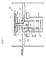
- Fig. 7 is a block diagram showing the configuration of a substrate rotating portion of the electron beam exposure device 10 according to a fourth embodiment of the present invention.
- An air bearing (air bearing) mechanism is used as a rotational bearing of the substrate rotating portion concerned.
- the bearing portion will be referred to as air bearing or bearing.
- the configuration other than the configuration relating to the substrate rotating portion is the same as the electron beam exposure device 10 of the first embodiment, etc.
- pressurized air from an air compressor (not shown) is supplied to the air bearing 51 through an air conduit pipe 52A at the introduction side.
- a spindle 53 is floated and held by the pressurized air, and a spindle shaft (hereinafter simply referred to as spindle) 53 is rotated by the spindle motor 54.
- the turntable 55 secured to the spindle 53 is rotated by rotation of the spindle 53, and the substrate 15 for the disc master mounted on the turntable 55 is rotated.
- 56 represents a steel cover.
- air from the air compressor is supplied to the turntable 55 through the air bearing 51 and the spindle 53. More specifically, a part of the pressurized air supplied from the air-compressor to the air bearing (hereinafter simply referred to as bearing) 51 is supplied to the turntable 55 through a conduit pipe 57A provided in the bearing 51 and a conduit pipe 57B provided in the spindle 53.
- the air supplied to the turntable 55 is circulated in the turntable 55 by the conduit pipe 57C provided in the turntable 55 to cool the turntable 55, that is, the substrate 15 mounted on the turntable 55.
- the conduit pipe 57C provided in the turntable 55 is preferably formed so that the supplied air is transported to the neighborhood of the upper surface of the turntable 55 adjacent to the substrate 15, whereby the substrate 15 is effectively cooled by the supplied air.
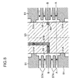
- Fig. 8 is a cross-sectional view showing the detailed structures of the bearing 51 and the spindle 53.
- the conduit pipe 57A provided in the bearing 51 is divided into plural feeding ports, for example, and intercommunicates with a gap portion (gap) 58 provided between the bearing 51 and the spindle 53.
- the gap 58 is formed so as to be spaced from the spindle 53 by about several ⁇ m, and it acts as an air bearing and also as an air in-take gap for introducing air into the conduit pipe 57B provided in the spindle 53.
- the bearing 51 is provided with a bearing projecting portion 51A that is spaced from the spindle 53 to the extent (for example, 1-2 ⁇ m) that gas (air) in the in-take gap 58 does not leak and surrounds the gap 58. That is, the area of the gap 58 is compartmented by the bearing projecting portion 51A.
- Figs. 9 and 10 are cross-sectional views showing the structures taken along line A-A and line B-B in Fig. 8.
- air is introduced from the conduit pipe 57A in the bearing 51 into the gap 58 between the spindle 53 having a cylindrical shape and the bearing 51.
- an annular groove 59 for introducing air into the conduit pipe 57B is formed at the outer peripheral portion of the spindle 53.
- the groove 59 is formed to be connected to the conduit pipe 57B. Accordingly, the air introduced in the gap 58 is taken into the conduit pipe 57B in the spindle 53 through the groove 59.
- the air taken into the conduit pipe 57B is supplied to the turntable 55 and circulated through the conduit pipe 57C in the turntable 55, thereby cooling the substrate 15 mounted on the turntable 55. According to the above-described configuration, the reaction of the resist during execution of the drawing (exposure) operation is suppressed, so that PED can be sufficiently suppressed.
- the fluid (air) for the bearing 51 can be used for cooling, so that it is unnecessary to particularly provide a supply/discharge device, a route, etc. for fluid for cooling the substrate, and the configuration of the cooling device can be simplified. Furthermore, it is sufficient only to cool the substrate 15 and thus it is unnecessary to perform complicated and bothersome adjustment.
- an air bearing is used as the bearing, however, gas other than air or fluid may be used.
- Fig. 11 is a block diagram showing the configuration of the substrate rotating portion of the electron beam exposure device 10 according to a fifth embodiment of the present invention.
- an introducing/discharging passage for fluid (air) for cooling is provided separately from the fluid passage for the bearing as in the case of the fourth embodiment described above.
- a cooling compressor 60 and a conduit pipe 61 for feeding cooling air are provided.
- the conduit 61 is connected to the cooling compressor 60 and the conduit pipe 57A.
- the cooling air from the cooling compressor 60 is passed through the conduit pipe 61, supplied to the conduit 57A in the bearing 51 and taken into the conduit pipe 57B in the spindle 53.
- the cooling medium is not limited to air, and other gas and liquid may be sued.
- another cooling passage which is different from the fluid (air) passage for the bearing 51 is provided in the bearing 51, the spindle 53 and the turntable 55, and the substrate 15 mounted on the turntable 55 is cooled by the cooling medium passing through the another cooling passage.
- the cooling conduits are provided in the bearing 51, the spindle 53 and the turntable 55, and thus the configuration of the cooling device can be simplified unlike a case where the cooling passage is provided at the outside of the bearing 51.
- Fig. 12 is a block diagram showing the configuration of the substrate rotating portion of the electron beam exposure device 10 according to a sixth embodiment of the present invention.
- a bearing portion and a cooling fluid supply portion are constructed independently of each other. That is, the bearing portion is not necessarily limited to the air bearing, and it may be other types of bearing such as a rolling bearing, a sliding bearing or the like.
- Fig. 12 shows a case where the bearing portion is constructed by a rolling bearing 63.
- the cooling fluid supply portion has a rotary joint structure, however, it may have another structure which can supply fluid to the rotating portion.
- the other configuration is the same as the fifth embodiment.
- the cooling air from the cooling compressor 60 is passed through the conduit pipe 61, and taken into the conduit pipe 57B in the spindle 53. According to the above configuration, the reaction of the resist during execution of the drawing (exposure) operation can be suppressed, and PED can be sufficiently suppressed.
- the cooling medium is not limited to air, and other gas or liquid may be used.
- the device when it is unnecessary to use the air bearing as the bearing portion, the device can be constructed more easily.
- Fig. 13 is a diagram showing the configuration of the electron beam exposure device 10 according to a seventh embodiment of the present invention.
- the electron beam exposure device 10 is provided with a vacuum chamber 11, an electron beam column 12, a rotating device 13 and a feeding device 14 for rotating and feeding the substrate 15 disposed in the vacuum chamber 11, various circuits for performing the operation control of the substrate, the electron beam control, etc., and a control system (not shown).
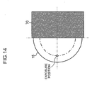
- Fig. 14 is a top view showing the arrangement of the substrate 15 and the low temperature member 70.
- the low temperature member 70 is disposed so as to be opposed to the exposure position (beam irradiation position) on the substrate 15 (i.e. , at the opposite side by 180 degrees). That is, by disposing the low temperature member 70 at a position different from the exposure position, the exposed portion is cooled by rotation of the substrate 15 after the exposure. That is, the heat of the substrate 15 (exposed resist portion) can be actively deprived by balance of radiation heat, whereby PED can be effectively suppressed.
- Fig. 15 is a top view showing the arrangement of the substrate 15 and the low temperature member 70.
- the low temperature member 70 is disposed at the downstream side of the rotation of the substrate with respect to the exposure position on the substrate 15. According to this configuration, the heat of the substrate 15 (exposed resist portion) can be actively deprived by the balance of the radiation heat, whereby PED can be effectively suppressed.
- an electron beam is used as an exposure beam, however, it may be applied to an exposure device using an optical beam such as a laser beam or the like.
- an exposure device using synchrotron radiation (SOR) light or the like the principal surface of the substrate 15 is disposed in the vertical direction (that is, the rotational axis is set to the horizontal direction), and in such a case, the low temperature member 70 may be disposed at the exposure surface side of the substrate.
Landscapes
- Engineering & Computer Science (AREA)
- Chemical & Material Sciences (AREA)
- Nanotechnology (AREA)
- Physics & Mathematics (AREA)
- General Engineering & Computer Science (AREA)
- Health & Medical Sciences (AREA)
- General Physics & Mathematics (AREA)
- Manufacturing & Machinery (AREA)
- Crystallography & Structural Chemistry (AREA)
- Mechanical Engineering (AREA)
- Epidemiology (AREA)
- Condensed Matter Physics & Semiconductors (AREA)
- Life Sciences & Earth Sciences (AREA)
- Atmospheric Sciences (AREA)
- Toxicology (AREA)
- Environmental & Geological Engineering (AREA)
- Analytical Chemistry (AREA)
- Public Health (AREA)
- Mathematical Physics (AREA)
- Theoretical Computer Science (AREA)
- Manufacturing Optical Record Carriers (AREA)
- Electron Beam Exposure (AREA)
- Exposure And Positioning Against Photoresist Photosensitive Materials (AREA)
Abstract
The device includes a substrate holding portion for holding a substrate having resist formed thereon, a driving portion for varying the irradiation position of an exposure beam relatively to the substrate, and a cooling portion for cooling the substrate during irradiation of the exposure beam.
Description
- The present invention relates to an exposure device, and particularly to an exposure device for carrying out exposure while moving the irradiation position of an exposure beam onto a substrate on which a resist is formed.
- A method using a chemical amplification type resist having high sensitivity and high resolution is used is known as a method of forming a fine pattern. According to the patterning method, exposure (drawing) using an electron beam, post-exposure bake (PEB: Post Exposure Bake) and development are carried out on a substrate coated with a chemical amplification resist. A predetermined time is needed from the drawing step till the PEB step, and the size of a pattern achieved after the development is varied between a portion drawn at the initial stage of drawing and a portion drawn at the last stage on the same substrate. This is caused by a phenomenon that the time required from the drawing step till the PEB step (post-exposure delay time or standby time) is varied in accordance with the position on the substrate and thus the same reaction as PEB progresses during the standby time. Furthermore, when a sheet-feed type treatment is carried out, the size of a pattern achieved after the development is varied in accordance with the treatment order of the substrate, for example, between the first drawn (or developed) substrate and the last drawn (or developed) substrate.
- The above-described problem is known as a PED (Post Exposure Delay) problem to the chemical amplification resist or the like. The development of resists has been continued to suppress the effect of the standby time as described above, however, a sufficient development has not yet been achieved.
- Furthermore, as a method of solving the problem are disclosed a method of controlling the PEB condition on the basis of the time from the drawing step to the PEB step and the standby time characteristic of the resist (see,
Japanese Laid-Open Patent Application Kokai No.08-111370 Japanese Laid-Open Patent Application Kokai No.10-172882 - However, for example, when drawing is carried out by using an electron beam, it takes much time to drawn the whole surface of the substrate, and the reaction progresses during the drawing time. For example, it takes about three hours to draw the whole surface of a disc of 120mm in diameter by using a chemical amplification resist. Furthermore, the electron beam is irradiated to the drawing substrate with energy of several KeV to 100kev, for example. In general, the resolution of the electron beam is dependent on the energy of the electron beam, and a high-energy electron beam is used when high resolution is achieved. A part of the energy of the electron beam is used for the exposure reaction of the resist. However, most of the other energy is converted to heat by scattering in the substrate, and the substrate is locally heated. Therefore, the reaction during the standby time is promoted by the heat.
- Accordingly, the related art described above has a problem that PED cannot be sufficiently controlled. Furthermore, the method of adjusting the PEB condition or the like has a drawback that the adjusting method and the adjusting condition are complicated and bothersome.
- The present invention has been made in view of the foregoing problems, and has an object to provide an inexpensive exposure device that can suppress PED (Post Exposure Delay) and achieve an excellently uniform pattern.
- In order to attain the above object, according to the present invention, an exposure device for irradiating an exposure beam to a substrate having a resist formed thereon to form a latent image on the resist is characterized by comprising a substrate holder for holding the substrate, a driving portion for relatively changing the irradiation position of the exposure beam to the substrate, and a cooling portion for cooling the substrate during the irradiation of the exposure beam.
- According to the present invention, an exposure device for irradiating an exposure beam to a substrate having a resist formed thereon to form a latent image is characterized by comprising a substrate holding portion for holding the substrate; a spindle for rotating the substrate holding portion; a fluid bearing portion for holding the spindle; and a conduit pipe that passes through the fluid bearing portion and the spindle to supply cooling fluid to the substrate holding portion.
- According to the present invention, an exposure device for irradiating an exposure beam to a disc-shaped substrate having a resist formed thereon to form a latent image on the resist is characterized by comprising a substrate holding portion for holding the substrate and rotating the substrate, an irradiation portion for irradiating the exposure beam to the substrate; and a low temperature member that is disposed above the substrate and at the rotational downstream side of the irradiation position of the exposure beam.
-
- Fig. 1 is a block diagram showing the configuration of an electron beam exposure device according to a first embodiment of the present invention;
- Fig. 2 is a diagram showing a cooling heat pipe provided in a turntable;
- Fig. 3 is a block diagram showing the configuration of an exposure device according to a second embodiment of the present invention;
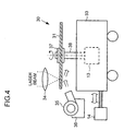
- Fig. 4 shows a modification of the second embodiment as shown in Fig. 3 and is a diagram showing a case where an air blower for cooling the substrate from the back surface side;
- Fig. 5 is a block diagram showing the configuration of an exposure device according to a third embodiment of the present invention;
- Fig. 6 is a block diagram showing the configuration of an exposure device according to a modification of the third embodiment of the present invention;
- Fig. 7 is a diagram showing the configuration of a substrate rotating portion of an electron beam exposure device according to a fourth embodiment of the present invention;
- Fig. 8 is a cross-sectional view showing the detailed structures of a bearing and a spindle;
- Fig. 9 is a cross-sectional view showing the structure taken along A-A line of Fig. 8;
- Fig. 10 is a cross-sectional view showing the structure taken along B-B line of Fig. 8;
- Fig. 11 is a block diagram showing the configuration of a substrate rotating portion of an electron beam exposure device according to a fifth embodiment of the present invention;
- Fig. 12 is a block diagram showing the configuration of a substrate rotating portion of an electron beam exposure device according to a sixth embodiment of the present invention;
- Fig. 13 is a block diagram showing the configuration of the substrate rotating portion of the electron beam exposure device according to the sixth embodiment of the present invention;
- Fig. 14 is a top view showing the arrangement of a substrate and a low temperature member; and
- Fig. 15 is a top view showing the arrangement of the substrate and the low temperature member.
- Embodiments according to the present invention will be described in detail. In the following embodiments, the equivalent constituent elements are represented by the same reference numerals.
- Fig. 1 is a block diagram showing the configuration of an electron
beam exposure device 10 according to a first embodiment of the present invention. The electronbeam exposure device 10 is a mastering device for creating a master disc such as a magnetic disc or an optical disc by using an electron beam. - The electron
beam exposure device 10 is equipped with avacuum chamber 11, anelectron beam column 12 secured to thevacuum chamber 11,driving devices vacuum chamber 11, various kinds of circuits for controlling the driving of the substrate, controlling the electron beam, etc., and a control system (not shown). - More specifically, the
substrate 15 for the disc master is mounted on aturntable 16. Theturntable 16 is provided on a rotating and feeding stage (hereinafter, simply referred to as stage) 17. Thestage 17 has aspindle motor 13 for rotating theturntable 16 on which thesubstrate 15 is mounted. Thestage 17 is coupled to afeeding motor 14 for translating theturntable 16. Accordingly, thesubstrate 15 can be moved in a predetermined direction in a plane parallel to the principal surface of thesubstrate 15 while rotating thesubstrate 15. Theturntable 16 may be equipped with an electrostatic chucking mechanism for holding thesubstrate 15 while chucking thesubstrate 15. Alternatively, theturntable 16 may be equipped with a configuration of mechanically pressing thesubstrate 15 so that thesubstrate 15 is in close contact with theturntable 16. - The
electron beam column 12 is provided with an electron gun (emitter) for emitting an electron beam, a lens for converging the electron beam, and an electrode, a coil, etc. (not shown) for deflecting the electron beam. An electron beam (EB) of electron beam current of several nA to several 100nA which is converged by an objective lens to have an energy of several KeV to several tens KeV is irradiated to the resist on thesubstrate 15. For example, the acceleration voltage of electrons being used is 50kV, and the electron beam current is set to 120nA. - If the electron beam current or the like is intensified, the exposure (drawing) can be finished in a shorter time. However, the heating of the irradiation of the electrode beam is increased, and thus the reactivity of the resist is enhanced.
- As shown in Fig. 2, a water cooling
type cooling device 18 is provided in theturntable 16. More specifically, thecooling device 18 is a heat pipe 18 (indicated by a broken line in Fig. 2) which is piped in thestage 17. Cooling medium such as cooling water or the like is supplied from the outside through theconduit pipe 19 is supplied to theheat pipe 18, whereby theturntable 16, that is, thesubstrate 15 can be cooled even during the exposure of the electron beam. In Fig. 2, arrows in theturntable 16 and thestage 17 indicate flow of heat. Accordingly, local heating of thesubstrate 15 due to irradiation of the electron beam can be avoided. The cooling of thesubstrate 15 described above is performed during at least the exposure period. - Accordingly, the reaction of the resist during execution of the drawing (i.e. , electron beam exposure) on the
substrate 15 can be suppressed, and PED can be sufficiently suppressed. Particularly, this effect is enhanced when an electron beam having high energy is used or electron beam current is increased, and the reaction of the resist can be effectively suppressed. Furthermore, since it is sufficient only to cool thesubstrate 15, and thus it is unnecessary to perform complicated and bothersome adjustment. - Fig. 3 is a block diagram showing the configuration of an
exposure device 30 according to a second embodiment of the present invention. Theexposure device 30 is a device for creating a master disc such as an optical disc or the like by using a laser light beam, for example. - In the
exposure device 30, asubstrate 31 for a mater disc is mounted on aturntable 32. Theturntable 32 is provided on astage 33. Theexposure device 30 has aspindle motor 13 for rotating theturntable 32 on which thesubstrate 31 is mounted, and a feedingmotor 14 for translating theturntable 32, whereby thesubstrate 31 can be moved in a predetermined direction in a plane parallel to the principal surface of thesubstrate 31 while rotating thesubstrate 31. Theexposure device 30 has an optical system for condensing a laser beam for beam exposure and irradiating the laser beam on thesubstrate 31. That is, the laser beam is condensed by anobjective lens 34, and the beam spot of the laser beam is irradiated onto a resist coated on thesubstrate 31 to perform beam exposure. - The
exposure device 30 is provided with an air blower (blower) 35. Theair blower 35 is designed to cool the turntable, that is, thesubstrate 31 even during exposure (drawing) operation. The orientation of theair blower 35 is settled so that air (air or cooled air) from theair blower 35 impinges against the surface of thesubstrate 31. As shown in Fig. 3, theair blower 35 is preferably secured to a movingdevice 36 which can adjust the orientation of theair blower 35. The orientation of theair blower 35 is adjusted so that the air blown from theair blower 35 impinges against the irradiation position of the laser beam on thesubstrate 31 - Next, a modification of the embodiment will be described with reference to Fig. 4.
- The
substrate 31 is partially held at only the center portion thereof by a substrate holder (chucking) 37, and fixed to the upper portion of arotational shaft 38 of thespindle motor 13. This modification is the same as the above embodiment in that thesubstrate 31 can be moved in a predetermined direction in a plane parallel to the principal surface of thesubstrate 31 with rotating thesubstrate 31 by thespindle motor 13 and the feedingmotor 14. - The
exposure device 30 is provided with an air blower (blower) 35. Theair blower 35 cools thesubstrate 31 from the back surface (the surface at the opposite side to the exposure surface of the substrate 31) of thesubstrate 31. Theair blower 35 is secured to the movingdevice 36 that can adjust the orientation of theair blower 35, and the orientation of theair blower 35 is adjusted so that the air blown from theair blower 35 impinges the back surface position of thesubstrate 31 corresponding to the irradiation position of the laser beam. - Accordingly, the heating of the
substrate 31 is suppressed, so that the reaction of the resist during the execution of the drawing (exposure) of thesubstrate 31 is suppressed, and PED can be sufficiently suppressed. Furthermore, since it is sufficient only to cool thesubstrate 31, it is unnecessary to perform complicated and bothersome adjustment. - Fig. 5 is a block diagram showing the configuration of an electron
beam exposure device 40 according to a third embodiment. The electronbeam exposure device 40 is a mastering device for creating a master disc such as a magnetic disc, an optical disc or the like by using an electron beam, for example. - The electron
beam exposure device 40 is provided with avacuum chamber 11, a driving device that is disposed in the vacuum chamber and rotates and translates a substrate while the substrate is disposed thereon, anelectron beam column 12 secured to thevacuum chamber 11, various kinds of circuits for controlling the driving of the substrate, the electron beam, etc., and a control system (not shown). - More specifically, the
substrate 15 for the disc master is put on theturntable 16. Theturntable 16 is provided on thestage 17. Thestage 17 has aspindle motor 13 for rotating theturntable 16 mounted on thesubstrate 15. Thestage 17 is coupled to a feedingmotor 14 for translating theturntable 16. Accordingly, thesubstrate 15 can be moved in a predetermined direction in a plane parallel to the principal surface of thesubstrate 15 while rotating thesubstrate 15. Theturntable 16 is provided with a mechanism for chucking thesubstrate 15 so that thesubstrate 15 is brought into close contact with theturntable 16. - As shown in Fig. 5, a cooling device 41 (indicated by a broken line in Fig. 5) that can electrically cool the substrate 15 (turntable 16) is provided in the
turntable 16. For example, a Peltier cooling device containing a Peltier element may be used as thecooling device 41. The description will be made by exemplifying a case where aPeltier cooling device 41 containing a Peltier element is used as thecooling device 41. Furthermore, atemperature sensor 42 having at least one detecting element such as a thermistor or the like is provided to detect the temperature of thesubstrate 15. In this embodiment, thetemperature sensor 42 has a plurality of detecting elements which are arranged in the radius (radial) direction of thesubstrate 15 in theturntable 16 so that the in-plane temperature distribution of thesubstrate 15 can be detected. - A detection signal from the
temperature sensor 42 is supplied to atemperature signal generator 43. Thetemperature signal generator 43 generates a temperature signal representing the temperature of thesubstrate 15 on the basis of the temperature detection signal concerned and transmits the temperature signal to atemperature controller 45. Aposition detector 44 generates an irradiation position signal representing the position on thesubstrate 15 to which the electron beam is irradiated, and transmits it to thetemperature controller 45. For example, the feedingmotor 14 is a stepping motor, and theposition detector 44 detects the beam irradiation position (the position in the radial direction) with respect to a reference position (for example, the center of the substrate) on the basis of the number of stepping pulses of the feedingmotor 14. - The
temperature controller 45 controls thecooling device 41 on the basis of the temperature detection signal and the irradiation position signal to cool the portion corresponding to the beam irradiation position at the back side of thesubstrate 15 locally and intensively. For this purpose, thecooling device 41 is divided into a plurality of cooling portions. For example, thecooling device 41 comprises plural Peltier elements arranged concentrically, and the Peltier element located at the radial position corresponding to the beam irradiation position is driven to cool thesubstrate 15. Accordingly, this effect is greater particularly when large electron beam current is used and the heating of the substrate 15 (resist) is locally increased, and the reaction of the resist can be effectively suppressed. - Alternatively, as a modification of the embodiment, the
temperature controller 45 may control thecooling device 41 merely on the basis of the temperature detection signal to uniformly cool thesubstrate 15 as shown in Fig. 6. Accordingly, in this case, noposition detector 44 may be provided. For example, thesubstrate 15 is cooled so that the temperature thereof is equal to a predetermined temperature (for example, room temperature) or less. - It is preferable that the cooling operation of the
substrate 15 is executed during at least the exposure period. - As various embodiments are described above, by cooling the substrate during execution of the drawing (exposure) operation, the reaction of the resist can be lowered, and PED can be sufficiently suppressed. The effect is particularly large when an electron beam having high energy is used or the electron beam current is increased to enhance the resolution, and the reaction of the resist can be effectively suppressed. Furthermore, there can be implemented an exposure device in which it is unnecessary to perform complicated and bothersome adjustment and a pattern having excellent uniformity can be easily achieved.
- The above-described embodiments may be properly combined with one another. For example, in the first embodiment, a cooling device using a Peltier element or the like may be sued in place of the cooling device using cooling water.
- Furthermore, the above-described embodiments relate to an exposure device using a so-called X-θ stage. However, the present invention is not limited to this embodiment, and each of the embodiments may relate to an X-Y type exposure device.
- Fig. 7 is a block diagram showing the configuration of a substrate rotating portion of the electron
beam exposure device 10 according to a fourth embodiment of the present invention. An air bearing (air bearing) mechanism is used as a rotational bearing of the substrate rotating portion concerned. In the following description, the bearing portion will be referred to as air bearing or bearing. The configuration other than the configuration relating to the substrate rotating portion is the same as the electronbeam exposure device 10 of the first embodiment, etc. - More specifically, pressurized air from an air compressor (not shown) is supplied to the
air bearing 51 through anair conduit pipe 52A at the introduction side. Aspindle 53 is floated and held by the pressurized air, and a spindle shaft (hereinafter simply referred to as spindle) 53 is rotated by thespindle motor 54. Theturntable 55 secured to thespindle 53 is rotated by rotation of thespindle 53, and thesubstrate 15 for the disc master mounted on theturntable 55 is rotated. 56 represents a steel cover. - In the embodiment, air from the air compressor is supplied to the
turntable 55 through theair bearing 51 and thespindle 53. More specifically, a part of the pressurized air supplied from the air-compressor to the air bearing (hereinafter simply referred to as bearing) 51 is supplied to theturntable 55 through aconduit pipe 57A provided in thebearing 51 and aconduit pipe 57B provided in thespindle 53. The air supplied to theturntable 55 is circulated in theturntable 55 by theconduit pipe 57C provided in theturntable 55 to cool theturntable 55, that is, thesubstrate 15 mounted on theturntable 55. Theconduit pipe 57C provided in theturntable 55 is preferably formed so that the supplied air is transported to the neighborhood of the upper surface of theturntable 55 adjacent to thesubstrate 15, whereby thesubstrate 15 is effectively cooled by the supplied air. - The structure of introducing air from the bearing 51 to the
spindle 53 will be described in detail with reference to Figs. 8 to 10. Fig. 8 is a cross-sectional view showing the detailed structures of thebearing 51 and thespindle 53. As shown in Fig. 8, theconduit pipe 57A provided in thebearing 51 is divided into plural feeding ports, for example, and intercommunicates with a gap portion (gap) 58 provided between the bearing 51 and thespindle 53. More specifically, thegap 58 is formed so as to be spaced from thespindle 53 by about several µm, and it acts as an air bearing and also as an air in-take gap for introducing air into theconduit pipe 57B provided in thespindle 53. Thebearing 51 is provided with abearing projecting portion 51A that is spaced from thespindle 53 to the extent (for example, 1-2 µm) that gas (air) in the in-take gap 58 does not leak and surrounds thegap 58. That is, the area of thegap 58 is compartmented by thebearing projecting portion 51A. - Figs. 9 and 10 are cross-sectional views showing the structures taken along line A-A and line B-B in Fig. 8. As shown in Fig. 9, air is introduced from the
conduit pipe 57A in thebearing 51 into thegap 58 between thespindle 53 having a cylindrical shape and thebearing 51. As shown in Figs. 8 and 9, anannular groove 59 for introducing air into theconduit pipe 57B is formed at the outer peripheral portion of thespindle 53. Furthermore, thegroove 59 is formed to be connected to theconduit pipe 57B. Accordingly, the air introduced in thegap 58 is taken into theconduit pipe 57B in thespindle 53 through thegroove 59. The air taken into theconduit pipe 57B is supplied to theturntable 55 and circulated through theconduit pipe 57C in theturntable 55, thereby cooling thesubstrate 15 mounted on theturntable 55. According to the above-described configuration, the reaction of the resist during execution of the drawing (exposure) operation is suppressed, so that PED can be sufficiently suppressed. - Accordingly, the fluid (air) for the
bearing 51 can be used for cooling, so that it is unnecessary to particularly provide a supply/discharge device, a route, etc. for fluid for cooling the substrate, and the configuration of the cooling device can be simplified. Furthermore, it is sufficient only to cool thesubstrate 15 and thus it is unnecessary to perform complicated and bothersome adjustment. In the foregoing description, an air bearing is used as the bearing, however, gas other than air or fluid may be used. - Fig. 11 is a block diagram showing the configuration of the substrate rotating portion of the electron
beam exposure device 10 according to a fifth embodiment of the present invention. In the embodiment, an introducing/discharging passage for fluid (air) for cooling is provided separately from the fluid passage for the bearing as in the case of the fourth embodiment described above. - More specifically, a cooling
compressor 60 and aconduit pipe 61 for feeding cooling air are provided. Theconduit 61 is connected to thecooling compressor 60 and theconduit pipe 57A. the cooling air from the coolingcompressor 60 is passed through theconduit pipe 61, supplied to theconduit 57A in thebearing 51 and taken into theconduit pipe 57B in thespindle 53. According to the above configuration, the reaction of the resist during execution of the drawing (exposure) operation on thesubstrate 15 can be suppressed and thus PED can be sufficiently suppressed. - As the case of the embodiment 4, the cooling medium is not limited to air, and other gas and liquid may be sued.
- Accordingly, in the embodiment, another cooling passage which is different from the fluid (air) passage for the
bearing 51 is provided in thebearing 51, thespindle 53 and theturntable 55, and thesubstrate 15 mounted on theturntable 55 is cooled by the cooling medium passing through the another cooling passage. In the embodiment, as in the case of the fourth embodiment, the cooling conduits are provided in thebearing 51, thespindle 53 and theturntable 55, and thus the configuration of the cooling device can be simplified unlike a case where the cooling passage is provided at the outside of thebearing 51. - Fig. 12 is a block diagram showing the configuration of the substrate rotating portion of the electron
beam exposure device 10 according to a sixth embodiment of the present invention. In the embodiment, a bearing portion and a cooling fluid supply portion are constructed independently of each other. That is, the bearing portion is not necessarily limited to the air bearing, and it may be other types of bearing such as a rolling bearing, a sliding bearing or the like. Fig. 12 shows a case where the bearing portion is constructed by a rollingbearing 63. The cooling fluid supply portion has a rotary joint structure, however, it may have another structure which can supply fluid to the rotating portion. The other configuration is the same as the fifth embodiment. - More specifically, the cooling air from the cooling
compressor 60 is passed through theconduit pipe 61, and taken into theconduit pipe 57B in thespindle 53. According to the above configuration, the reaction of the resist during execution of the drawing (exposure) operation can be suppressed, and PED can be sufficiently suppressed. - As the case of the above-described embodiments, the cooling medium is not limited to air, and other gas or liquid may be used.
- Accordingly, when it is unnecessary to use the air bearing as the bearing portion, the device can be constructed more easily.
- Fig. 13 is a diagram showing the configuration of the electron
beam exposure device 10 according to a seventh embodiment of the present invention. The electronbeam exposure device 10 is provided with avacuum chamber 11, anelectron beam column 12, arotating device 13 and afeeding device 14 for rotating and feeding thesubstrate 15 disposed in thevacuum chamber 11, various circuits for performing the operation control of the substrate, the electron beam control, etc., and a control system (not shown). - In the embodiment, a
low temperature member 70 for cooling thesubstrate 15 and aconduit pipe 71 for supplying cooling medium to thelow temperature member 70. - Fig. 14 is a top view showing the arrangement of the
substrate 15 and thelow temperature member 70. Specifically, thelow temperature member 70 is disposed so as to be opposed to the exposure position (beam irradiation position) on the substrate 15 (i.e. , at the opposite side by 180 degrees). That is, by disposing thelow temperature member 70 at a position different from the exposure position, the exposed portion is cooled by rotation of thesubstrate 15 after the exposure. That is, the heat of the substrate 15 (exposed resist portion) can be actively deprived by balance of radiation heat, whereby PED can be effectively suppressed. - Fig. 15 is a top view showing the arrangement of the
substrate 15 and thelow temperature member 70. Specifically, thelow temperature member 70 is disposed at the downstream side of the rotation of the substrate with respect to the exposure position on thesubstrate 15. According to this configuration, the heat of the substrate 15 (exposed resist portion) can be actively deprived by the balance of the radiation heat, whereby PED can be effectively suppressed. - In the foregoing description, an electron beam is used as an exposure beam, however, it may be applied to an exposure device using an optical beam such as a laser beam or the like. Furthermore, in an exposure device using synchrotron radiation (SOR) light or the like, the principal surface of the
substrate 15 is disposed in the vertical direction (that is, the rotational axis is set to the horizontal direction), and in such a case, thelow temperature member 70 may be disposed at the exposure surface side of the substrate. -
- 10, 30, 40
- exposure device
- 15
- Substrate
- 17, 33
- Stage
- 18, 41
- Cooling device
- 42
- Temperature sensor
- 43
- Temperature signal generator
- 44
- Position detector
- 45
- Temperature controller
- EB
- Electron beam
- 51
- Bearing
- 53
- Spindle
- 55
- Turntable
- 57A, 57B, 57C, 57D
- Conduit pipe
- 63
- Rolling bearing
- 70
- Low temperature member
Claims (12)
- An exposure device for irradiating an exposure beam to a substrate having a resist formed thereon to form a latent image on the resist, comprising:a substrate holding portion for holding the substrate;a driving portion for varying an irradiation position of the exposure beam relatively to the substrate; anda cooling portion for cooling the substrate during irradiation of the exposure beam.
- The exposure device according to claim 1, further comprising: an irradiation position detector for detecting the irradiation position of the exposure beam; a temperature detector for detecting the temperature at the irradiation position; and a temperature controller for controlling the temperature of the irradiation position on the basis of the temperature detected by the temperature detector.
- The exposure device according to claim 1, wherein the substrate is mounted on the substrate holding portion and the cooling portion is a cooling pipe provided in the substrate holding portion.
- The exposure device according to any one of claims 1 to 3, wherein the exposure beam is an electron beam.
- The exposure device according to claim 1, wherein the resist is a chemical amplification resist.
- The exposure device according to claim 1, wherein the exposure beam is a light beam, and the cooling portion is a cooling device.
- An exposure device for irradiating an exposure beam to a substrate having a resist formed thereon, comprising:a substrate mount portion for holding the substrate;a spindle for rotating the substrate mount portion;a fluid bearing portion for holding the spindle; anda conduit pipe for supplying cooling fluid through the fluid bearing portion and the spindle to the substrate mount portion.
- The exposure device according to claim 7, wherein the spindle has a groove portion through which the cooling fluid supplied through the fluid bearing portion is taken into the conduit pipe provided in the spindle.
- The exposure device according to claim 7, further comprising a cooling fluid supply portion and a cooling fluid supply conduit pipe for supplying cooling fluid from the cooling fluid supply portion to the conduit pipe provided in the spindle.
- An exposure device for irradiating an exposure beam to a substrate having a resist formed thereon, comprising:a substrate mount portion for holding the substrate;a spindle for rotating the substrate mount portion;a bearing portion for holding the spindle, anda cooling fluid supply portion and a cooling fluid supply conduit pipe, provided independently of the bearing portion, for supplying cooling fluid from the cooling fluid supply portion to a conduit pipe provided in the spindle.
- An exposure device for irradiating an exposure beam to a disc-shaped substrate having a resist formed thereon to form a latent image on the resist, comprising:a substrate mount portion for holding the substrate and rotating the substrate;an irradiating portion for irradiating the exposure beam to the substrate; anda low temperature member that is disposed at the exposure surface side of the substrate and at the rotational downstream side of the irradiation position of the exposure beam.
- The exposure device according to claim 11, wherein the low temperature member is disposed at the exposure surface side of the substrate and at the opposite side to the irradiation position with respect to the center of the substrate.
Applications Claiming Priority (2)
| Application Number | Priority Date | Filing Date | Title |
|---|---|---|---|
| JP2004097471 | 2004-03-30 | ||
| PCT/JP2005/006525 WO2005096101A1 (en) | 2004-03-30 | 2005-03-28 | Exposure equipment |
Publications (2)
| Publication Number | Publication Date |
|---|---|
| EP1731966A1 true EP1731966A1 (en) | 2006-12-13 |
| EP1731966A4 EP1731966A4 (en) | 2008-01-16 |
Family
ID=35063954
Family Applications (1)
| Application Number | Title | Priority Date | Filing Date |
|---|---|---|---|
| EP05727502A Withdrawn EP1731966A4 (en) | 2004-03-30 | 2005-03-28 | Exposure equipment |
Country Status (4)
| Country | Link |
|---|---|
| US (1) | US20070182942A1 (en) |
| EP (1) | EP1731966A4 (en) |
| JP (1) | JP4256893B2 (en) |
| WO (1) | WO2005096101A1 (en) |
Cited By (1)
| Publication number | Priority date | Publication date | Assignee | Title |
|---|---|---|---|---|
| CN103488054A (en) * | 2012-06-07 | 2014-01-01 | 株式会社有泽制作所 | Exposure apparatus and exposure method |
Families Citing this family (3)
| Publication number | Priority date | Publication date | Assignee | Title |
|---|---|---|---|---|
| JP5561989B2 (en) * | 2009-10-02 | 2014-07-30 | 太陽ホールディングス株式会社 | Pattern formation method using laser |
| US10384299B2 (en) * | 2013-06-26 | 2019-08-20 | Apple Inc. | Electron beam conditioning |
| JP2017199610A (en) * | 2016-04-28 | 2017-11-02 | 株式会社ニューフレアテクノロジー | Stage mechanism |
Family Cites Families (23)
| Publication number | Priority date | Publication date | Assignee | Title |
|---|---|---|---|---|
| US3930684A (en) * | 1971-06-22 | 1976-01-06 | Lasch Jr Cecil A | Automatic wafer feeding and pre-alignment apparatus and method |
| JPS57149731A (en) * | 1981-03-11 | 1982-09-16 | Seiko Epson Corp | Exposing device |
| US4676649A (en) * | 1985-11-27 | 1987-06-30 | Compact Spindle Bearing Corp. | Multi-axis gas bearing stage assembly |
| JPH01152639A (en) * | 1987-12-10 | 1989-06-15 | Canon Inc | Chuck |
| JPH0750680B2 (en) * | 1988-12-28 | 1995-05-31 | ウシオ電機株式会社 | Wafer edge exposure system |
| JP2949547B2 (en) * | 1993-02-08 | 1999-09-13 | 東京エレクトロン株式会社 | Processing device and processing method |
| JPH0837144A (en) * | 1994-07-25 | 1996-02-06 | Kawasaki Steel Corp | Pattern transfer exposure method and exposure apparatus |
| US6113702A (en) * | 1995-09-01 | 2000-09-05 | Asm America, Inc. | Wafer support system |
| JPH0992613A (en) * | 1995-09-21 | 1997-04-04 | Nikon Corp | Temperature control device and scanning exposure device |
| US6005226A (en) * | 1997-11-24 | 1999-12-21 | Steag-Rtp Systems | Rapid thermal processing (RTP) system with gas driven rotating substrate |
| US6098408A (en) * | 1998-11-11 | 2000-08-08 | Advanced Micro Devices | System for controlling reflection reticle temperature in microlithography |
| JP4143216B2 (en) * | 1999-04-20 | 2008-09-03 | 新明和工業株式会社 | Air spindle |
| TW513617B (en) * | 1999-04-21 | 2002-12-11 | Asml Corp | Lithographic projection apparatus and method of manufacturing a device using a lithographic projection apparatus |
| US6214121B1 (en) * | 1999-07-07 | 2001-04-10 | Applied Materials, Inc. | Pedestal with a thermally controlled platen |
| JP2001229583A (en) * | 2000-02-16 | 2001-08-24 | Hitachi Ltd | Master exposure apparatus and method |
| JP2001250278A (en) * | 2000-03-02 | 2001-09-14 | Hitachi Ltd | Master exposure apparatus and method |
| JP3870002B2 (en) * | 2000-04-07 | 2007-01-17 | キヤノン株式会社 | Exposure equipment |
| DE60129377T2 (en) * | 2000-06-02 | 2008-03-20 | Asml Netherlands B.V. | Lithographic projection apparatus with a support arrangement |
| JP2002083758A (en) * | 2000-09-07 | 2002-03-22 | Pioneer Electronic Corp | Exposure equipment |
| US6689221B2 (en) * | 2000-12-04 | 2004-02-10 | Applied Materials, Inc. | Cooling gas delivery system for a rotatable semiconductor substrate support assembly |
| JP4745556B2 (en) * | 2001-08-20 | 2011-08-10 | キヤノン株式会社 | Positioning apparatus, exposure apparatus, and device manufacturing method |
| KR20030033219A (en) * | 2001-10-19 | 2003-05-01 | 삼성전자주식회사 | Edge exposure apparatus for semiconductor wafer |
| JP4307130B2 (en) * | 2003-04-08 | 2009-08-05 | キヤノン株式会社 | Exposure equipment |
-
2005
- 2005-03-28 US US10/593,744 patent/US20070182942A1/en not_active Abandoned
- 2005-03-28 WO PCT/JP2005/006525 patent/WO2005096101A1/en not_active Ceased
- 2005-03-28 EP EP05727502A patent/EP1731966A4/en not_active Withdrawn
- 2005-03-28 JP JP2006511854A patent/JP4256893B2/en not_active Expired - Fee Related
Cited By (1)
| Publication number | Priority date | Publication date | Assignee | Title |
|---|---|---|---|---|
| CN103488054A (en) * | 2012-06-07 | 2014-01-01 | 株式会社有泽制作所 | Exposure apparatus and exposure method |
Also Published As
| Publication number | Publication date |
|---|---|
| JP4256893B2 (en) | 2009-04-22 |
| US20070182942A1 (en) | 2007-08-09 |
| EP1731966A4 (en) | 2008-01-16 |
| WO2005096101A1 (en) | 2005-10-13 |
| JPWO2005096101A1 (en) | 2008-02-21 |
Similar Documents
| Publication | Publication Date | Title |
|---|---|---|
| US4465934A (en) | Parallel charged particle beam exposure system | |
| US7025005B2 (en) | Stage device and angle detecting device | |
| US7189979B2 (en) | Electron gun | |
| US6333572B1 (en) | Article positioning apparatus and exposing apparatus having the article positioning apparatus | |
| US6616762B2 (en) | Treatment solution supply apparatus and treatment solution supply method | |
| JP2001242300A (en) | Electron beam irradiation device | |
| US7602472B2 (en) | Contamination prevention system, lithographic apparatus, radiation source, and method for manufacturing a device | |
| JP2578093B2 (en) | Electronic image projector | |
| JP2986080B2 (en) | Rotary reticle scanning projection lithography apparatus and method | |
| US5831274A (en) | Apparatus for image transfer with charged particle beam, and deflector and mask used with such apparatus | |
| EP1731966A1 (en) | Exposure equipment | |
| EP1542263A1 (en) | Electron beam exposure method and system therefor | |
| JP4261751B2 (en) | Rotation drive device and disk master production device using the same | |
| EP0069728A4 (en) | Parallel charged particle beam exposure system. | |
| JP2001307385A (en) | Method and apparatus for manufacturing optical disk master | |
| JP4886984B2 (en) | Electron beam drawing device | |
| US20240079264A1 (en) | Substrate supporting apparatus | |
| Thornton | Electron physics in device microfabrication. II electron resists, X-ray lithography, and electron beam lithography update | |
| US20130092837A1 (en) | Pattern inspection device and pattern inspection method | |
| JP2002203774A (en) | Electron beam irradiation method and electron beam irradiation device | |
| JP3347634B2 (en) | Electron beam lithography system | |
| JP2002222748A (en) | Electron beam irradiation method and electron beam irradiation device | |
| JP2003331480A (en) | Method for producing master for producing optical recording medium and method for producing stamper for producing optical recording medium | |
| JP2006210459A (en) | Charged particle beam exposure apparatus, charged particle beam exposure method, and device manufacturing method | |
| JP2001319844A (en) | Charged particle beam exposure apparatus, charged particle beam exposure method, and device manufacturing method |
Legal Events
| Date | Code | Title | Description |
|---|---|---|---|
| PUAI | Public reference made under article 153(3) epc to a published international application that has entered the european phase |
Free format text: ORIGINAL CODE: 0009012 |
|
| 17P | Request for examination filed |
Effective date: 20060911 |
|
| AK | Designated contracting states |
Kind code of ref document: A1 Designated state(s): DE FR GB SE |
|
| DAX | Request for extension of the european patent (deleted) | ||
| RBV | Designated contracting states (corrected) |
Designated state(s): DE FR GB SE |
|
| A4 | Supplementary search report drawn up and despatched |
Effective date: 20071218 |
|
| STAA | Information on the status of an ep patent application or granted ep patent |
Free format text: STATUS: THE APPLICATION HAS BEEN WITHDRAWN |
|
| 18W | Application withdrawn |
Effective date: 20080411 |