EP1729341A2 - Semiconductor IC and its manufacturing method, and module with embedded semiconductor IC and its manufacturing method - Google Patents
Semiconductor IC and its manufacturing method, and module with embedded semiconductor IC and its manufacturing method Download PDFInfo
- Publication number
- EP1729341A2 EP1729341A2 EP06252853A EP06252853A EP1729341A2 EP 1729341 A2 EP1729341 A2 EP 1729341A2 EP 06252853 A EP06252853 A EP 06252853A EP 06252853 A EP06252853 A EP 06252853A EP 1729341 A2 EP1729341 A2 EP 1729341A2
- Authority
- EP
- European Patent Office
- Prior art keywords
- semiconductor
- metal layer
- integrated circuit
- main body
- embedded
- Prior art date
- Legal status (The legal status is an assumption and is not a legal conclusion. Google has not performed a legal analysis and makes no representation as to the accuracy of the status listed.)
- Withdrawn
Links
Images




Classifications
-
- H—ELECTRICITY
- H10—SEMICONDUCTOR DEVICES; ELECTRIC SOLID-STATE DEVICES NOT OTHERWISE PROVIDED FOR
- H10W—GENERIC PACKAGES, INTERCONNECTIONS, CONNECTORS OR OTHER CONSTRUCTIONAL DETAILS OF DEVICES COVERED BY CLASS H10
- H10W40/00—Arrangements for thermal protection or thermal control
- H10W40/10—Arrangements for heating
-
- H—ELECTRICITY
- H10—SEMICONDUCTOR DEVICES; ELECTRIC SOLID-STATE DEVICES NOT OTHERWISE PROVIDED FOR
- H10F—INORGANIC SEMICONDUCTOR DEVICES SENSITIVE TO INFRARED RADIATION, LIGHT, ELECTROMAGNETIC RADIATION OF SHORTER WAVELENGTH OR CORPUSCULAR RADIATION
- H10F77/00—Constructional details of devices covered by this subclass
- H10F77/93—Interconnections
-
- H—ELECTRICITY
- H10—SEMICONDUCTOR DEVICES; ELECTRIC SOLID-STATE DEVICES NOT OTHERWISE PROVIDED FOR
- H10W—GENERIC PACKAGES, INTERCONNECTIONS, CONNECTORS OR OTHER CONSTRUCTIONAL DETAILS OF DEVICES COVERED BY CLASS H10
- H10W40/00—Arrangements for thermal protection or thermal control
- H10W40/70—Fillings or auxiliary members in containers or in encapsulations for thermal protection or control
- H10W40/77—Auxiliary members characterised by their shape
- H10W40/778—Auxiliary members characterised by their shape in encapsulations
-
- H—ELECTRICITY
- H10—SEMICONDUCTOR DEVICES; ELECTRIC SOLID-STATE DEVICES NOT OTHERWISE PROVIDED FOR
- H10W—GENERIC PACKAGES, INTERCONNECTIONS, CONNECTORS OR OTHER CONSTRUCTIONAL DETAILS OF DEVICES COVERED BY CLASS H10
- H10W70/00—Package substrates; Interposers; Redistribution layers [RDL]
- H10W70/01—Manufacture or treatment
- H10W70/05—Manufacture or treatment of insulating or insulated package substrates, or of interposers, or of redistribution layers
- H10W70/08—Manufacture or treatment of insulating or insulated package substrates, or of interposers, or of redistribution layers by depositing layers on the chip or wafer, e.g. "chip-first" RDLs
- H10W70/09—Manufacture or treatment of insulating or insulated package substrates, or of interposers, or of redistribution layers by depositing layers on the chip or wafer, e.g. "chip-first" RDLs extending onto an encapsulation that laterally surrounds the chip or wafer, e.g. fan-out wafer level package [FOWLP] RDLs
-
- H—ELECTRICITY
- H10—SEMICONDUCTOR DEVICES; ELECTRIC SOLID-STATE DEVICES NOT OTHERWISE PROVIDED FOR
- H10W—GENERIC PACKAGES, INTERCONNECTIONS, CONNECTORS OR OTHER CONSTRUCTIONAL DETAILS OF DEVICES COVERED BY CLASS H10
- H10W70/00—Package substrates; Interposers; Redistribution layers [RDL]
- H10W70/01—Manufacture or treatment
- H10W70/05—Manufacture or treatment of insulating or insulated package substrates, or of interposers, or of redistribution layers
- H10W70/093—Connecting or disconnecting other interconnections thereto or therefrom, e.g. connecting bond wires or bumps
-
- H—ELECTRICITY
- H10—SEMICONDUCTOR DEVICES; ELECTRIC SOLID-STATE DEVICES NOT OTHERWISE PROVIDED FOR
- H10W—GENERIC PACKAGES, INTERCONNECTIONS, CONNECTORS OR OTHER CONSTRUCTIONAL DETAILS OF DEVICES COVERED BY CLASS H10
- H10W74/00—Encapsulations, e.g. protective coatings
- H10W74/10—Encapsulations, e.g. protective coatings characterised by their shape or disposition
- H10W74/111—Encapsulations, e.g. protective coatings characterised by their shape or disposition the semiconductor body being completely enclosed
- H10W74/129—Encapsulations, e.g. protective coatings characterised by their shape or disposition the semiconductor body being completely enclosed forming a chip-scale package [CSP]
-
- H—ELECTRICITY
- H10—SEMICONDUCTOR DEVICES; ELECTRIC SOLID-STATE DEVICES NOT OTHERWISE PROVIDED FOR
- H10W—GENERIC PACKAGES, INTERCONNECTIONS, CONNECTORS OR OTHER CONSTRUCTIONAL DETAILS OF DEVICES COVERED BY CLASS H10
- H10W70/00—Package substrates; Interposers; Redistribution layers [RDL]
- H10W70/099—Connecting interconnections to insulating or insulated package substrates, interposers or redistribution layers
-
- H—ELECTRICITY
- H10—SEMICONDUCTOR DEVICES; ELECTRIC SOLID-STATE DEVICES NOT OTHERWISE PROVIDED FOR
- H10W—GENERIC PACKAGES, INTERCONNECTIONS, CONNECTORS OR OTHER CONSTRUCTIONAL DETAILS OF DEVICES COVERED BY CLASS H10
- H10W72/00—Interconnections or connectors in packages
- H10W72/01—Manufacture or treatment
- H10W72/012—Manufacture or treatment of bump connectors, dummy bumps or thermal bumps
- H10W72/01221—Manufacture or treatment of bump connectors, dummy bumps or thermal bumps using local deposition
- H10W72/01225—Manufacture or treatment of bump connectors, dummy bumps or thermal bumps using local deposition in solid form, e.g. by using a powder or by stud bumping
-
- H—ELECTRICITY
- H10—SEMICONDUCTOR DEVICES; ELECTRIC SOLID-STATE DEVICES NOT OTHERWISE PROVIDED FOR
- H10W—GENERIC PACKAGES, INTERCONNECTIONS, CONNECTORS OR OTHER CONSTRUCTIONAL DETAILS OF DEVICES COVERED BY CLASS H10
- H10W72/00—Interconnections or connectors in packages
- H10W72/01—Manufacture or treatment
- H10W72/0198—Manufacture or treatment batch processes
-
- H—ELECTRICITY
- H10—SEMICONDUCTOR DEVICES; ELECTRIC SOLID-STATE DEVICES NOT OTHERWISE PROVIDED FOR
- H10W—GENERIC PACKAGES, INTERCONNECTIONS, CONNECTORS OR OTHER CONSTRUCTIONAL DETAILS OF DEVICES COVERED BY CLASS H10
- H10W72/00—Interconnections or connectors in packages
- H10W72/071—Connecting or disconnecting
- H10W72/072—Connecting or disconnecting of bump connectors
- H10W72/07251—Connecting or disconnecting of bump connectors characterised by changes in properties of the bump connectors during connecting
-
- H—ELECTRICITY
- H10—SEMICONDUCTOR DEVICES; ELECTRIC SOLID-STATE DEVICES NOT OTHERWISE PROVIDED FOR
- H10W—GENERIC PACKAGES, INTERCONNECTIONS, CONNECTORS OR OTHER CONSTRUCTIONAL DETAILS OF DEVICES COVERED BY CLASS H10
- H10W72/00—Interconnections or connectors in packages
- H10W72/071—Connecting or disconnecting
- H10W72/073—Connecting or disconnecting of die-attach connectors
-
- H—ELECTRICITY
- H10—SEMICONDUCTOR DEVICES; ELECTRIC SOLID-STATE DEVICES NOT OTHERWISE PROVIDED FOR
- H10W—GENERIC PACKAGES, INTERCONNECTIONS, CONNECTORS OR OTHER CONSTRUCTIONAL DETAILS OF DEVICES COVERED BY CLASS H10
- H10W72/00—Interconnections or connectors in packages
- H10W72/20—Bump connectors, e.g. solder bumps or copper pillars; Dummy bumps; Thermal bumps
-
- H—ELECTRICITY
- H10—SEMICONDUCTOR DEVICES; ELECTRIC SOLID-STATE DEVICES NOT OTHERWISE PROVIDED FOR
- H10W—GENERIC PACKAGES, INTERCONNECTIONS, CONNECTORS OR OTHER CONSTRUCTIONAL DETAILS OF DEVICES COVERED BY CLASS H10
- H10W72/00—Interconnections or connectors in packages
- H10W72/20—Bump connectors, e.g. solder bumps or copper pillars; Dummy bumps; Thermal bumps
- H10W72/251—Materials
- H10W72/252—Materials comprising solid metals or solid metalloids, e.g. PbSn, Ag or Cu
-
- H—ELECTRICITY
- H10—SEMICONDUCTOR DEVICES; ELECTRIC SOLID-STATE DEVICES NOT OTHERWISE PROVIDED FOR
- H10W—GENERIC PACKAGES, INTERCONNECTIONS, CONNECTORS OR OTHER CONSTRUCTIONAL DETAILS OF DEVICES COVERED BY CLASS H10
- H10W72/00—Interconnections or connectors in packages
- H10W72/20—Bump connectors, e.g. solder bumps or copper pillars; Dummy bumps; Thermal bumps
- H10W72/29—Bond pads specially adapted therefor
-
- H—ELECTRICITY
- H10—SEMICONDUCTOR DEVICES; ELECTRIC SOLID-STATE DEVICES NOT OTHERWISE PROVIDED FOR
- H10W—GENERIC PACKAGES, INTERCONNECTIONS, CONNECTORS OR OTHER CONSTRUCTIONAL DETAILS OF DEVICES COVERED BY CLASS H10
- H10W72/00—Interconnections or connectors in packages
- H10W72/50—Bond wires
- H10W72/59—Bond pads specially adapted therefor
-
- H—ELECTRICITY
- H10—SEMICONDUCTOR DEVICES; ELECTRIC SOLID-STATE DEVICES NOT OTHERWISE PROVIDED FOR
- H10W—GENERIC PACKAGES, INTERCONNECTIONS, CONNECTORS OR OTHER CONSTRUCTIONAL DETAILS OF DEVICES COVERED BY CLASS H10
- H10W72/00—Interconnections or connectors in packages
- H10W72/851—Dispositions of multiple connectors or interconnections
- H10W72/874—On different surfaces
-
- H—ELECTRICITY
- H10—SEMICONDUCTOR DEVICES; ELECTRIC SOLID-STATE DEVICES NOT OTHERWISE PROVIDED FOR
- H10W—GENERIC PACKAGES, INTERCONNECTIONS, CONNECTORS OR OTHER CONSTRUCTIONAL DETAILS OF DEVICES COVERED BY CLASS H10
- H10W72/00—Interconnections or connectors in packages
- H10W72/851—Dispositions of multiple connectors or interconnections
- H10W72/874—On different surfaces
- H10W72/877—Bump connectors and die-attach connectors
-
- H—ELECTRICITY
- H10—SEMICONDUCTOR DEVICES; ELECTRIC SOLID-STATE DEVICES NOT OTHERWISE PROVIDED FOR
- H10W—GENERIC PACKAGES, INTERCONNECTIONS, CONNECTORS OR OTHER CONSTRUCTIONAL DETAILS OF DEVICES COVERED BY CLASS H10
- H10W72/00—Interconnections or connectors in packages
- H10W72/90—Bond pads, in general
- H10W72/941—Dispositions of bond pads
- H10W72/9413—Dispositions of bond pads on encapsulations
-
- H—ELECTRICITY
- H10—SEMICONDUCTOR DEVICES; ELECTRIC SOLID-STATE DEVICES NOT OTHERWISE PROVIDED FOR
- H10W—GENERIC PACKAGES, INTERCONNECTIONS, CONNECTORS OR OTHER CONSTRUCTIONAL DETAILS OF DEVICES COVERED BY CLASS H10
- H10W90/00—Package configurations
- H10W90/701—Package configurations characterised by the relative positions of pads or connectors relative to package parts
- H10W90/731—Package configurations characterised by the relative positions of pads or connectors relative to package parts of die-attach connectors
- H10W90/736—Package configurations characterised by the relative positions of pads or connectors relative to package parts of die-attach connectors between a chip and a stacked lead frame, conducting package substrate or heat sink
Definitions
- the present invention relates to a semiconductor integrated circuit (hereinafter, "semiconductor IC") and a method of manufacturing the same.
- semiconductor IC semiconductor integrated circuit
- the invention relates to a semiconductor IC that can be suitably embedded in a circuit board, and a method of manufacturing this semiconductor IC.
- the present invention also relates to a module with embedded semiconductor IC, and a method of manufacturing the same.
- the invention relates to a module with embedded semiconductor IC having excellent heat dissipation, and a method of manufacturing this module with embedded semiconductor IC.
- a semiconductor IC with a metal plate adhered to the back surface is proposed so as to improve heat dissipation from a semiconductor IC, as described in Japanese Patent Laid Open No. 2003-174116 .
- the semiconductor IC described in Japanese Patent Laid Open No. 2003-174116 is manufactured as follows.
- a metal plate is adhered to the back surface of a wafer, via a welding sheet. Thereafter, the wafer is divided into individual semiconductor ICs, by dicing.
- the semiconductor wafer has a rigid and fragile characteristic, and the metal plate has high extension characteristic. Therefore, it is practically very difficult to dice without problem a laminate made of different kinds of materials having greatly different physical characteristics. Specifically, when the laminate made of different kinds of materials is diced, very severe chipping or extension occurs on the disconnected surface, and the semiconductor ICs cannot be practically used.
- a module with embedded semiconductor IC that has a semiconductor IC built in the circuit board, applied by the applicant of the present invention, is also described in Japanese Patent Laid Open No. 2005-64470 .
- a large part of the embedded semiconductor IC is covered with a resin. Therefore, heat dissipation is not satisfactory.
- a semiconductor IC to be built in is thinned in advance, thereby decreasing a total thickness of the module with embedded semiconductor IC.
- a metal plate is adhered in a wafer state to improve heat dissipation as described in Japanese Patent Laid Open No. 2003-174116 , large warpage occurs in the semiconductor wafer, due to a difference between a thermal expansion coefficient of the semiconductor wafer and a thermal expansion coefficient of the metal plate. As a result, easiness of handling and productivity decrease.
- dicing becomes considerably difficult, as described above.
- the present invention has been achieved to solve the above problems. It is therefore an object of the present invention to provide a semiconductor IC that can obtain high heat dissipation even when the semiconductor IC is embedded in a circuit board and that can be manufactured easily using a process of a printed circuit, and provide a method of manufacturing this semiconductor IC.
- the semiconductor IC according to the present invention includes a semiconductor IC main body on the main surface of which a predetermined circuit is formed, and a metal layer selectively provided at the center of the back surface of the semiconductor IC main body.
- the semiconductor IC can have high heat dissipation, using a metal layer provided at the center of the back surface of the semiconductor IC main body. Because the metal layer is selectively provided, warpage does not occur easily in the wafer state, even when the semiconductor IC main body is thinned by polishing or the like. Because a position at which the metal layer is selectively provided is the center of the back surface of the semiconductor IC main body, it is not necessary to dice the laminate of the semiconductor wafer and the thick metal. As a result, chipping of the disconnected surface can be prevented effectively.
- the metal layer is provided on substantially the whole back surface of the semiconductor IC main body except the periphery of the back surface.
- the metal layer is provided on substantially the whole back surface of the semiconductor IC main body, higher heat dissipation can be obtained.
- the semiconductor IC according to the present invention further includes an under-barrier metal layer provided between at least the metal layer and the back surface of the semiconductor IC main body.
- an under-barrier metal layer provided between at least the metal layer and the back surface of the semiconductor IC main body. In the presence of the under-barrier metal layer, close adhesion between the metal layer and the semiconductor IC main body can be increased.
- the semiconductor IC according to the present invention further includes a rust preventing film that covers the bottom surface and the side surface of the metal layer.
- a rust preventing film that covers the bottom surface and the side surface of the metal layer.
- the rust preventing film is selectively provided in a region of the back surface of the semiconductor IC main body except the periphery of the back surface. According to this arrangement, chipping of the disconnected surface can be prevented at the time of dicing the semiconductor wafer, because the rust preventing film is not present in the dicing region.
- a method of manufacturing a semiconductor IC according to the present invention includes: a first step for selectively forming a metal layer on the back surface of a semiconductor wafer on the main surface of which a predetermined circuit is formed; and a second step for disconnecting the semiconductor wafer along a region in which the metal layer is not formed.
- the metal layer is selectively provided. Therefore, warpage does not occur easily in the wafer state, even when the semiconductor IC main body is thinned by polishing or the like. Furthermore, chipping of the disconnected surface can be prevented effectively at the dicing time.
- the first process includes: a step for forming an under-barrier metal layer on substantially the whole back surface of the semiconductor wafer; and a step for selectively forming the metal layer on the under-barrier metal layer, by plating while covering a part of the under-barrier metal layer with a resist.
- a step for forming an under-barrier metal layer on substantially the whole back surface of the semiconductor wafer a step for selectively forming the metal layer on the under-barrier metal layer, by plating while covering a part of the under-barrier metal layer with a resist.
- the first process further includes:
- the method of manufacturing a semiconductor IC includes a step for thinning the semiconductor wafer before performing the first process.
- the semiconductor IC is embedded in the resin layer, the total of the module with embedded semiconductor IC can be thinned.
- the method of manufacturing a semiconductor IC further includes a step for forming a rust preventing film that covers the bottom surface and the side surface of the metal layer after performing the first step and before performing the second step.
- this rust preventing film is provided, the occurrence of oxidation and corrosion can be prevented, even when a material that can easily generate oxidation or corrosion is used as a material of the metal layer.
- the rust preventing film is selectively formed on substantially the whole back surface of the semiconductor wafer, except at least a part of the region of the back surface not covered with the metal layer. According to this arrangement, chipping of the disconnected surface can be prevented at the time of dicing the semiconductor wafer, because the rust preventing film is not present in the dicing region.
- the method of manufacturing a semiconductor IC further includes a step for roughening the surface of the metal layer.
- a semiconductor IC when a semiconductor IC is embedded in a resin layer, close adhesion between the semiconductor IC and the resin layer can be further increased.
- the bottom surface of the resin layer forms substantially the same plane as the bottom surface of the metal layer provided on the semiconductor IC main body.
- substantially the whole surface of the metal layer becomes in an exposed state. Therefore, remarkably high heat dissipation can be obtained.
- a method of manufacturing a module with embedded semiconductor IC according to the present invention includes: a first step for embedding the semiconductor IC in a resin layer; and a second step for exposing at least a part of the surface of the metal layer provided on the semiconductor IC main body. According to the present invention, the metal layer of the semiconductor IC embedded in the resin layer is exposed. Therefore, a module with embedded semiconductor IC having high heat dissipation can be provided.
- the second process can be performed by exposing substantially the whole bottom surface of the metal layer by polishing the bottom surface of the resin layer, or can be performed by exposing at least a part of the bottom surface of the metal layer by forming via holes on the bottom surface of the resin layer.
- the method of manufacturing a module with embedded semiconductor IC further includes a third step for embedding the via holes with a material having higher thermal conductivity than that of the resin layer.
- heat can be efficiently dissipated from the surface of the metal layer exposed in the second process, via the embedded material.
- a material having high thermal conductivity preferably a material including a filler in conductive or insulating paste can be used, in addition to metal.
- FIG. 1 is a schematic cross-sectional view of a configuration of a semiconductor IC 10 according to a preferred embodiment of the present invention.
- the semiconductor IC 10 includes: a semiconductor IC main body 11 on a main surface 11a of which a predetermined circuit (not shown) is formed; an under-barrier metal layer 12 provided at the center of a back surface 11b of the semiconductor IC main body 11; and a metal layer 13 provided on the under-barrier metal layer 12.
- the semiconductor IC 10 While any types of IC can be used as the semiconductor IC 10, a digital IC having a very high operation frequency such as a CPU and a DSP can be selectively used. This kind of semiconductor IC generates a large amount of heat by high-speed switching. As described later, the semiconductor IC 10 according to the present embodiment can dissipate heat to a motherboard remarkably efficiently, even when the semiconductor IC 10 is embedded in the multilayer substrate. Therefore, a digital IC that generates a large amount of heat can be selected.
- Pad electrodes 14 are formed on the main surface 11a of the semiconductor IC main body 11.
- a stud bump 15 as one kind of a conductive projection is formed on each of the pad electrodes 14.
- the semiconductor IC can be connected to a wiring by forming via holes by emitting a laser beam or by polishing. As described later, the semiconductor IC 10 can be positioned in the manufacture of a module with embedded semiconductor IC.
- the conductive projection is not limited to the stud bump 15, and various kinds of bumps such as a plate bump, a plated bump, and a ball bump can be used.
- a stud bump is used as a conductive projection, silver or copper can be wire bonded to form this stud bump.
- a plate bump is used, this can be formed by plating, sputtering, or by deposition.
- a plated bump is used, this can be formed by plating.
- a ball bump a solder ball is mounted on a land electrode, and is fused to from the ball bump, or a cream solder is printed on a land electrode, and is fused to from the ball bump.
- a kind of metal that can be used for the conductive projection is not particularly limited.
- gold (Au), silver (Ag), copper (Cu), nickel (Ni), tin (Sn), chrome (Cr), nickel chrome alloy (Ni-Cr), and solder can be used.
- a conductive material is screen printed, and is cured to form a conical or cylindrical bump. Nanopaste can be printed, heated, and sintered to form a bump.
- the semiconductor IC main body 11 has a thickness t (a distance from the main surface 11a to the back surface 11b) smaller than that of a normal semiconductor IC.
- the thickness t of the semiconductor IC main body 11 is not particularly limited.
- the thickness t is equal to or smaller than 100 micrometers, for example, about 20 to 50 micrometers. This is because when the thickness t of the semiconductor IC main body is smaller, the total thickness of the module with embedded semiconductor IC can be decreased.
- the semiconductor IC 10 according to the present embodiment has the metal layer 13. Therefore, occurrence of cracks can be prevented more effectively, and easiness of handling is more improved.
- the under-barrier metal layer 12 works to increase close adhesion between the semiconductor IC main body 11 and the metal layer 13.
- the urider-barrier metal layer 12 is selectively provided on substantially the whole back surface 11b of the semiconductor IC main body 11, excluding the periphery 11c of the back surface 11b.
- the metal layer 13 is formed by electrolytic plating, as described later. Therefore, the under-barrier metal layer 12 also works as a power supply film.
- a material of the under-barrier metal layer 12 is not particularly limited so long as the material meets the above objects.
- a material that can be used includes titanium (Ti), chrome (Cr), nickel (Ni), nickel chrome alloy (Ni-Cr), and a laminate of these metals, such as nickel/chrome (Ni/Cr).
- the above material is used as a ground material, and copper (Cu) is laminated on this surface, thereby forming the under-barrier metal layer 12.
- a film thickness of the under-barrier metal layer 12 is not particularly limited, and is preferably about 0.05 to 2 micrometers.
- a thickness of the chrome (Cr) is set to about 0.5 micrometer
- a thickness of the copper (Cu) laminated on this surface is set to about 0.5 micrometer.
- the under-barrier metal layer 12 can be formed by sputtering or depositing.
- the copper (Cu) can be formed on the surface of the ground material by electroless plating.
- the metal layer 13 is formed on the under-barrier metal layer 12 by electroless plating, and is selectively provided on substantially the whole back surface 11b of the semiconductor IC main body 11, excluding the periphery 11c of the back surface 11b.
- the metal layer 13 works as a heat dissipation route of heat generated by the operation of the semiconductor IC main body 11. At the same time, the metal layer 13 works to effectively prevent the occurrence of cracks on the back surface 11b of the semiconductor IC main body 11, and to improve easiness of handling.
- a material of the metal layer 13 is not particularly limited, so long as the material is a metal that can be formed by plating.
- the material that can be used includes copper (Cu), silver (Ag), gold (Au), titanium (Ti), chrome (Cr), nickel (Ni), nickel chrome alloy (Ni-Cr), solder, and tin (Sn).
- copper (Cu) is selected as a material of the metal layer 13, copper sulfate liquid or the like can be used for plating liquid.
- a film thickness of the metal layer 13 is not particularly limited, the thickness is preferably about 1 to 50 micrometers, and more preferably about 2 to 20 micrometers. Particularly, the thickness of about 5 to 15 micrometers is preferable. This is because when the film thickness of the metal layer 13 is less than one micrometer, effect of crack prevention and effect of improving handling easiness cannot be obtained sufficiently. Furthermore, there is a risk of addition of damage to the semiconductor IC main body, at the time of exposing a part of the metal layer 13 by laser irradiation, after the semiconductor IC 10 is embedded in a multilayer substrate.
- a film thickness of the metal layer 13 exceeds 50 micrometers, a thickness of the module with embedded semiconductor IC manufactured last becomes larger than is necessary. Accordingly, the effect of thinning the semiconductor IC main body 11 is halved.
- the above effect can be sufficiently obtained while decreasing the thickness of the module with embedded semiconductor IC. Furthermore, it becomes possible to decrease the risk of addition of damage to the semiconductor IC main body 11, at the time of exposing at least a part of the metal layer 13 by laser irradiation, after the semiconductor IC 10 is embedded in a multilayer substrate.
- the configuration of the semiconductor IC 10 according to the present embodiment is as explained above.
- a method of manufacturing the semiconductor IC 10 according to the present embodiment is explained below.
- FIG. 2 is a flowchart showing a method of manufacturing the semiconductor IC 10
- FIG. 3 to FIG. 10 are process diagrams along the flowchart shown in FIG. 2.
- a stress-relief processing is performed to the polished back surface 90b of the semiconductor wafer 90, thereby relaxing physical stress of the back surface 90b generated by the polishing (step S11).
- the stress relief processing includes wet etching using an etching liquid, polishing using slurry, dry polishing using a non-diamond abrasive coating, and dry etching using etching gas.
- the under-barrier metal layer 12 is formed on the whole back surface 90b of the semiconductor wafer 90 that has been stress-relief processed (step S12).
- a method of forming the under-barrier metal layer 12 use of sputtering and deposition is preferable.
- a resist 91 is formed on the whole surface of the under-barrier metal layer 12 (step S13).
- the resist 91 is patterned by exposing (step S14). Accordingly, a part of the under-barrier metal layer 12 is covered with the resist 91, and the remaining part of this layer is exposed.
- the part of the under-barrier metal layer 12 covered with the resist 91 is a region to be disconnected by dicing, and its vicinity. Therefore, the patterned resist 91 forms a grating that separates each semiconductor IC, as shown in a partial top plan view in FIG. 6.
- the metal layer 13 is formed on the under-barrier metal layer 12, by electrolytic plating, using the exposed under-barrier metal layer 12 as a power supply film (step S15). Accordingly, the metal layer 13 is selectively formed on the under-barrier metal layer 12.
- the resist 91 is removed (step S16), and an unnecessary part of the under-barrier metal layer 12 on which the metal layer 13 is not formed is removed by soft etching, as shown in FIG. 9 (step S17) . Accordingly, the back surface 90b of the semiconductor wafer 90 is covered with the under-barrier metal layer 12 and the metal layer 13 at the part corresponding to each semiconductor IC, and is exposed in the dicing region and its vicinity.
- the semiconductor wafer 90 is then diced along a line A-A, that is, along the exposed region not covered with the under-barrier metal layer 12 and the metal layer 13, thereby taking out individual semiconductor ICs 10 (step S18). Because the under-barrier metal layer 12 and the metal layer 13 are not formed but the semiconductor wafer 90 is exposed in the region to be diced, a normal dicer that is optimized to disconnect the semiconductor wafer can be used.
- the stud bumps 15 can be formed at any stage, for example, before thinning the semiconductor wafer 90 (step S10).
- a surface of the metal layer 13 is roughened, after the metal layer 13 is formed.
- a roughening method includes intergranular corrosion using hydrogen peroxide/sulfuric acid or formic acid, and tanning. Furthermore, instead of roughening the surface of the metal layer 13, the surface of the metal layer 13 can be rough plated, thereby roughening the surface.
- the semiconductor IC 10 shown in FIG. 1 is then completed in the method as described above.
- Removing the under-barrier metal layer 12 at step S17 is not essential. That is, dicing can be performed along a line B-B, while leaving the unnecessary part of the under-barrier metal layer 12 on which the metal layer 13 is not formed, as shown in FIG. 10 (step S18). With this arrangement, the soft etching process (step S17) can be omitted.
- the thin under-barrier metal layer 12 is still present in the area to be diced. Therefore, the dicing condition needs to be different from a normal condition in some cases, to avoid the occurrence of chipping. However, because the under-barrier metal layer 12 has a very small film thickness, the dicing condition of avoiding the chipping is not so strict.
- the metal layer 13 is selectively formed. Therefore, it is possible to avoid warpage that occurs when a thick metal layer is formed on the whole surface of the thinned semiconductor wafer 90.
- the region in which the metal layer 13 is not formed corresponds to a region to be diced. Therefore, the laminate of the semiconductor wafer and the thick metal does not need to be diced. As a result, chipping of the disconnected surface can be effectively prevented.
- FIG. 11 is a schematic cross-sectional view of a configuration of a semiconductor IC 20 according to another preferred embodiment of the present invention.
- the semiconductor IC 20 according to the present embodiment is the same as the semiconductor IC 10 according to the above embodiment, except that the semiconductor IC 20 includes a rust preventing film 21 that covers the back surface. Therefore, identical constituent elements are assigned with like reference numerals, and their redundant explanation is omitted.
- the rust preventing film 21 covers the back surface of the semiconductor IC 20, that is, the bottom surface and the side surface of the semiconductor IC 20 on which the metal layer 13 and the under-barrier metal layer 12 are exposed, and also covers the back surface 11b of the semiconductor IC main body 11 that is exposed at the periphery 11c.
- the rust preventing film 21 works to prevent corrosion of the metal layer 13 and to increase close adhesion between the resin and the semiconductor IC 20.
- a materia-1 of the rust preventing film 21 is not particularly limited so long as the material meets the above objects.
- the material used includes titanium (Ti), chrome (Cr), nickel (Ni), nickel-chrome alloy (Ni-Cr), and a laminate of these metals, such as nickel/chrome (Ni/Cr).
- a film thickness of the rust preventing film 21 is not particularly limited, and is preferably about 0.005 to 0.5 micrometer. As an example, when chrome (Cr) is used, the film thickness is set to about 0. 05 micrometer.
- the semiconductor IC 20 according to the present embodiment has the rust preventing film 21 that covers the metal layer 13, oxidation and corrosion of the metal layer 13 can be effectively prevented, even when a corrosive material such as copper (Cu) is selected for the material of the metal layer 13. As a result, high reliability can be obtained.
- a corrosive material such as copper (Cu)
- a process of forming the rust preventing film 21 by sputtering is added to between the process of removing the under-barrier metal layer (step S17) and the process of dicing (step S18).
- the dicing is performed in the state that the thin rust preventing film 21 is present in the region to be diced, as explained with reference to FIG. 10. Therefore, the dicing needs to be performed in the condition of not generating chipping.
- the rust preventing film 21 has a very small thickness like the under-barrier metal layer 12, the dicing condition that avoids chipping is not so strict.
- the surface of the metal layer 13 is roughened after the metal layer 13 is formed and before the rust preventing film 21 is formed.
- the rust preventing film 21 has a very small thickness, the roughened surface of the metal layer 13 is reflected to the rust preventing film 21. As a result, close adhesion between the metal layer 13 and the resin can be further improved.
- the rust preventing film 21 is selectively formed in the region of the semiconductor IC main body 11, excluding the periphery 11c.
- a metal mask 92 for covering the region to be disconnected by dicing and its vicinity is used, and selective sputtering or deposition can be performed via an opening 92a of the metal mask 92, as shown in FIG. 12.
- the rust preventing film 21 is formed on substantially the whole surface excluding at least a part not covered by the metal layer 13. Therefore, when the semiconductor wafer 90 is diced along a line C-C as shown in FIG. 13, individual semiconductor ICs 20 can be easily obtained, without generating chipping.
- a module with embedded semiconductor IC that has the semiconductor IC 10 embedded in a module is explained next.
- FIG. 14 a schematic cross-sectional view of a configuration of a module with embedded semiconductor IC 100 according to a preferred embodiment of the present invention.
- the module with embedded semiconductor IC 100 includes: a multilayer substrate 110 consisting of laminated resin layers 111 and 112; the semiconductor IC 10 embedded in the multilayer substrate 110; an internal conductive pattern 120 formed within the multilayer substrate 110; and a heat dissipation electrode 130 provided on a bottom surface 110a of the multilayer substrate 110.
- the module with embedded semiconductor IC 100 also includes a signal terminal electrode and a power source terminal electrode connected to the internal conductive pattern 120.
- these electrodes are not directly relevant to the gist of the present invention, and are, therefore, not shown in FIG. 14.
- the semiconductor IC 10 shown in FIG. 1 is embedded in the module with embedded semiconductor IC 100 according to the present embodiment, the semiconductor IC 20 shown in FIG. 11 can be also embedded, in place of the semiconductor IC 10.
- the module with embedded semiconductor IC 100 is mounted on a motherboard so that the mounting surface of the motherboard (not shown) faces the bottom surface 110a of the multilayer substrate 110.
- a ground pattern provided on the mounting surface of the motherboard and a heat dissipation electrode 130 provided on the module with embedded semiconductor IC 100 are electrically and mechanically connected to each other.
- a material of the resin layers 111 and 112 can be a thermosetting resin or a thermoplastic resin having reflow durability.
- any material can be selected from among an epoxy resin, bismalaimide-triazine resin (BT resin), a phenol resin, a vinyl benzene resin, a polyphenylene ether (polyphenylene etheroxide) resin (PPE, PPO), a cyanate resin, a benzooxyazine resin, a polyimide resin, aromatic polyester resin, polyphenylene sulfide resin, a polyetherimide resin, a polyarilate resin, and a polyetheretherketone resin.
- a material of unwoven cloth such as glass cloth, aramid, aromatic polyester that is impregnated with one of the above resins can be also used.
- a material of the above resin that is impregnated with a filler can be also used.
- the module with embedded semiconductor IC 100 incorporates the thinned semiconductor IC 10. Therefore, the total module with embedded semiconductor IC 100 can be thinned.
- the metal layer 13 provided on the semiconductor IC 10 is exposed on the bottom surface 110a of the multilayer substrate 110, and the heat dissipation electrode 130 is directly formed on the exposed metal layer 13.
- FIG. 15 to FIG. 19 are process diagrams sequentially depicting a method of manufacturing the module with embedded semiconductor IC 100.
- the prepreg is a sheet of fiber such as glass fiber and aramid fiber that is impregnated with an uncured thermosetting resin such as an epoxy resin.
- an uncured thermosetting resin such as an epoxy resin.
- the bottom surface of the resin layer 111 embedded with the semiconductor IC 10 is polished, thereby removing a part of the resin layer 111 up to a line D-D shown in FIG. 16.
- the metal layer 13 of the semiconductor IC 10 is exposed, and the bottom surface of the resin layer 111 forms substantially the same plane as the front surface of the metal layer 13.
- the upper surface of the resin layer 111 is then polished, thereby removing a part of the resin layer 111 up to a line E-E shown in FIG. 17, and exposing a part of the stud bumps 15 of the semiconductor IC 10 as show in FIG. 18.
- the internal conductive layer 120 is formed to be connected to the exposed stud bump 15, and the resin layer 112 that covers the internal conductive layer 120 is formed. Furthermore, the heat dissipation electrode 130 is formed, thereby completing the module with embedded semiconductor IC 100 shown in FIG. 14.
- the module with embedded semiconductor IC 100 is manufactured in the above method, substantially the whole surface of the metal layer 13 can be exposed. Therefore, a configuration having remarkably high heat dissipation can be obtained.
- the metal layer 13 has a smaller thickness, high precision is required to adjust the amount of polishing the resin layer 111.
- the metal layer 13 has a certain level of thickness (preferably equal to or larger than 5 micrometers), higher precision is not required to adjust the amount of polishing, and polishing can be performed easily.
- the metal layer 13 of the semiconductor IC 10 is exposed by polishing the bottom surface of the resin layer 111.
- the method of exposing the metal layer 13 is not limited to this.
- via holes 111c can be formed in the resin layer 111, by irradiating a laser beam, thereby exposing a part of the metal layer 13.
- a material 111d having higher thermal conductivity than that of the resin layer 111 is embedded in the via holes 111c, and the heat dissipation electrode 130 is formed on the surface of the embedded material 111d.
- the thickness of the metal layer 13 is too small, there is a risk that the semiconductor wafer 90 is directly damaged by energy of the irradiated laser beam, and the circuit such as the transistor formed on the semiconductor IC 10 is damaged.
- the metal layer 13 has a certain level of thickness (preferably equal to or larger than 5 micrometers), occurrence of this damage can be prevented.
- Either one of or both a metal and a conductive adhesive can be used for the embedded material 111d.
- metal is used for the embedded material 111d, this can be formed by plating.
- the embedded material 111d is completely filled.
- Plating and a conductive or insulating paste can be used together, or a conductive adhesive can be used.
- the embedded material 111d can be formed by screen printing.
- the sidewall of the via holes 111c is covered with metal, and the inside is filled with the conductive or insulating paste.
- the paste preferably contains a filler to increase thermal conductivity.
- the stud bumps 15 of the semiconductor IC 10 are exposed by polishing the upper surface of the resin layer 111.
- via holes 111e can be formed in the resin layer 111 by irradiating a laser beam, thereby exposing a part of a conductive projection such as the stud bumps 15.
- the bottom surface of the resin layer 111 is polished to expose the metal layer 13 of the semiconductor IC 10. Thereafter, the internal conductive pattern 120 is formed, and the resin layer 112 is formed to cover the internal conductive pattern 120.
- the resin layer 112 is formed to cover the internal conductive pattern 120.
- a part of the semiconductor IC 100 up to a line F-F can be removed by polishing.
- the pitch of the pad electrodes 14 provided on the semiconductor IC 10 is very small, for example, when the pitch is equal to or smaller than 100 micrometers, particularly about 60 micrometers, high precision is required in the positioning of the pad electrodes 14 and the internal conductive pattern 120. In this case, it is effective to perform positioning using conductive projections such as the stud bumps 15 provided on the pad electrodes 14.
- a transfer plate 190 formed with positioning holes 191 and an internal conductive pattern 120 is prepared in advance.
- An adhesive sheet 200 is laminated on this.
- the stud bumps 15 of the semiconductor IC 10 are engaged with the positioning holes 191, and are provisionally stopped.
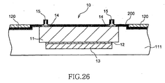
- the prepreg 111a and the transfer substrate 190 are pressed, and the transfer substrate 190 is peeled off.
- the internal conductive pattern 120 and the semiconductor IC 10 are embedded in the resin layer 111.
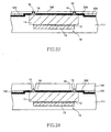
- the transfer substrate 190 is polished, after the internal conductive pattern 120 and the semiconductor IC 10 are embedded, thereby exposing the stud bumps 15, as shown in FIG. 27.
- the transfer substrate 190 is irradiated with a laser beam to form via holes, thereby exposing the stud bumps 15, as shown in FIG. 28.
- a positional relationship between the internal conductive pattern 120 and the stud bumps 15 of the semiconductor IC 10 is prescribed by the transfer substrate 190. Therefore, no positional deviation occurs between the internal conductive pattern 120 and the stud bumps 15 of the semiconductor IC 10. Consequently, even when the pitch of the pad electrodes 14 provided on the semiconductor IC 10 is very small, it becomes possible to prevent the occurrence of a positional deviation between the stud bumps 15 and the internal conductive pattern 120.
- the via holes 111c are formed in the resin layer 111 by irradiating a laser beam, thereby exposing a part of the metal layer 13.
- other internal conductive pattern 120 and the resin layer 112 are formed, and bumps of the heat dissipation electrode 130 are formed, thereby completing the module with embedded semiconductor IC.
- the module with embedded semiconductor IC 100 incorporates the thinned semiconductor IC 10, and can dissipate, remarkably efficiently, heat generated by the operation of the semiconductor IC 10, to the motherboard. Therefore, the invention can provide a thin module embedded with a digital IC having a very high operation frequency such as a CPU and a DSP.
- the semiconductor IC according to the present invention can obtain high thermal conductivity, even when the semiconductor IC is embedded in a circuit board made of resin. Therefore, the present can be very suitably applied to a semiconductor IC having high heat generation such as a CPU and a DSP. Because a metal layer is selectively provided, warpage does not occur in the wafer state, even when the semiconductor IC main body is thinned by polishing. Accordingly, the semiconductor IC can be manufactured easily.
- the metal layer is provided at the center of the back surface of the semiconductor IC main body, a laminate of the semiconductor wafer and the thick metal does not need to be diced. As a result, chipping of the disconnected surface can be prevented effectively. Consequently, a thin module with embedded semiconductor IC having high heat dissipation can be manufactured, by embedding this semiconductor IC in a multilayer substrate.
Landscapes
- Encapsulation Of And Coatings For Semiconductor Or Solid State Devices (AREA)
- Cooling Or The Like Of Semiconductors Or Solid State Devices (AREA)
Abstract
Description
- The present invention relates to a semiconductor integrated circuit (hereinafter, "semiconductor IC") and a method of manufacturing the same. Particularly, the invention relates to a semiconductor IC that can be suitably embedded in a circuit board, and a method of manufacturing this semiconductor IC. The present invention also relates to a module with embedded semiconductor IC, and a method of manufacturing the same. Particularly, the invention relates to a module with embedded semiconductor IC having excellent heat dissipation, and a method of manufacturing this module with embedded semiconductor IC.
- In recent years, in order to meet the requirement for a compact and thin module with embedded semiconductor IC, there have been many proposals of mounting a semiconductor IC in a bare chip state on a circuit board. However, when a semiconductor IC is mounted on the surface of the circuit board, a part of the surface of the circuit board is occupied by the semiconductor IC. Accordingly, utilization efficiency of the circuit board decreases. Furthermore, because the semiconductor IC is mounted on the circuit board, it has been difficult to decrease the total thickness of the module.
- In order to solve the above problems, it is proposed that a method of configuring a module with embedded semiconductor IC by forming a cavity on the circuit board. A semiconductor IC in a bare chip state is then embedded in the cavity. See
Japanese Patent Laid Open No. H9-321408 - However, according to the method described in
Japanese Patent Laid Open No. H9-321408 - A semiconductor IC with a metal plate adhered to the back surface is proposed so as to improve heat dissipation from a semiconductor IC, as described in
Japanese Patent Laid Open No. 2003-174116 Japanese Patent Laid Open No. 2003-174116 - A metal plate is adhered to the back surface of a wafer, via a welding sheet. Thereafter, the wafer is divided into individual semiconductor ICs, by dicing. However, the semiconductor wafer has a rigid and fragile characteristic, and the metal plate has high extension characteristic. Therefore, it is practically very difficult to dice without problem a laminate made of different kinds of materials having greatly different physical characteristics. Specifically, when the laminate made of different kinds of materials is diced, very severe chipping or extension occurs on the disconnected surface, and the semiconductor ICs cannot be practically used.
- A module with embedded semiconductor IC that has a semiconductor IC built in the circuit board, applied by the applicant of the present invention, is also described in
Japanese Patent Laid Open No. 2005-64470 Japanese Patent Laid Open No. 2005-64470 - According to the module with embedded semiconductor IC described in
Japanese Patent Laid Open No. 2005-64470 Japanese Patent Laid Open No. 2003-174116 - The present invention has been achieved to solve the above problems. It is therefore an object of the present invention to provide a semiconductor IC that can obtain high heat dissipation even when the semiconductor IC is embedded in a circuit board and that can be manufactured easily using a process of a printed circuit, and provide a method of manufacturing this semiconductor IC.
- It is another object of the present invention to provide a module with embedded semiconductor IC that has a semiconductor IC having above characteristics built in a module, and provide a method of manufacturing the module with embedded semiconductor IC.
- The semiconductor IC according to the present invention includes a semiconductor IC main body on the main surface of which a predetermined circuit is formed, and a metal layer selectively provided at the center of the back surface of the semiconductor IC main body.
- According to the present invention, the semiconductor IC can have high heat dissipation, using a metal layer provided at the center of the back surface of the semiconductor IC main body. Because the metal layer is selectively provided, warpage does not occur easily in the wafer state, even when the semiconductor IC main body is thinned by polishing or the like. Because a position at which the metal layer is selectively provided is the center of the back surface of the semiconductor IC main body, it is not necessary to dice the laminate of the semiconductor wafer and the thick metal. As a result, chipping of the disconnected surface can be prevented effectively.
- Preferably, the metal layer is provided on substantially the whole back surface of the semiconductor IC main body except the periphery of the back surface. When the metal layer is provided on substantially the whole back surface of the semiconductor IC main body, higher heat dissipation can be obtained.
- Preferably, the semiconductor IC according to the present invention further includes an under-barrier metal layer provided between at least the metal layer and the back surface of the semiconductor IC main body. In the presence of the under-barrier metal layer, close adhesion between the metal layer and the semiconductor IC main body can be increased.
- Preferably, the semiconductor IC according to the present invention further includes a rust preventing film that covers the bottom surface and the side surface of the metal layer. When this rust preventing film is provided, the occurrence of oxidation and corrosion can be prevented, even when a material that can easily generate oxidation or corrosion is used as a material of the metal layer.
- When a semiconductor IC is embedded in a resin layer, close adhesion between the semiconductor IC main body and the resin layer can be increased. Preferably, the rust preventing film is selectively provided in a region of the back surface of the semiconductor IC main body except the periphery of the back surface. According to this arrangement, chipping of the disconnected surface can be prevented at the time of dicing the semiconductor wafer, because the rust preventing film is not present in the dicing region.
- A method of manufacturing a semiconductor IC according to the present invention includes: a first step for selectively forming a metal layer on the back surface of a semiconductor wafer on the main surface of which a predetermined circuit is formed; and a second step for disconnecting the semiconductor wafer along a region in which the metal layer is not formed.
- According to the present invention, the metal layer is selectively provided. Therefore, warpage does not occur easily in the wafer state, even when the semiconductor IC main body is thinned by polishing or the like. Furthermore, chipping of the disconnected surface can be prevented effectively at the dicing time.
- Preferably, the first process includes: a step for forming an under-barrier metal layer on substantially the whole back surface of the semiconductor wafer; and a step for selectively forming the metal layer on the under-barrier metal layer, by plating while covering a part of the under-barrier metal layer with a resist. According to this method, close adhesion between the metal layer and the semiconductor IC main body can be increased. Furthermore, the metal layer can be selectively formed easily.
- Preferably, the first process further includes:
- a step for removing the resist after selectively forming the metal layer; and a step for removing the under-barrier metal layer exposed by removing the resist. According to this arrangement, chipping of the disconnected surface can be prevented at the time of dicing the semiconductor wafer, because the rust preventing film is not present in the dicing region.
- Preferably, the method of manufacturing a semiconductor IC includes a step for thinning the semiconductor wafer before performing the first process. According to this method, when the semiconductor IC is embedded in the resin layer, the total of the module with embedded semiconductor IC can be thinned.
- Preferably, the method of manufacturing a semiconductor IC further includes a step for forming a rust preventing film that covers the bottom surface and the side surface of the metal layer after performing the first step and before performing the second step. When this rust preventing film is provided, the occurrence of oxidation and corrosion can be prevented, even when a material that can easily generate oxidation or corrosion is used as a material of the metal layer.
- Preferably, the rust preventing film is selectively formed on substantially the whole back surface of the semiconductor wafer, except at least a part of the region of the back surface not covered with the metal layer. According to this arrangement, chipping of the disconnected surface can be prevented at the time of dicing the semiconductor wafer, because the rust preventing film is not present in the dicing region.
- Preferably, the method of manufacturing a semiconductor IC further includes a step for roughening the surface of the metal layer. According to this method, when a semiconductor IC is embedded in a resin layer, close adhesion between the semiconductor IC and the resin layer can be further increased.
- A module with embedded semiconductor IC according to the present invention includes the semiconductor IC and a resin layer into which the semiconductor IC is embedded. According to the semiconductor IC, high heat dissipation can be obtained using the metal layer provided at the center of the back surface of the semiconductor IC main body. Therefore, it is possible to provide a thin module with embedded semiconductor IC that has a semiconductor IC built in to generate a large amount of heat by high-speed switching.
- Preferably, the bottom surface of the resin layer forms substantially the same plane as the bottom surface of the metal layer provided on the semiconductor IC main body. With this arrangement, substantially the whole surface of the metal layer becomes in an exposed state. Therefore, remarkably high heat dissipation can be obtained.
- A method of manufacturing a module with embedded semiconductor IC according to the present invention includes: a first step for embedding the semiconductor IC in a resin layer; and a second step for exposing at least a part of the surface of the metal layer provided on the semiconductor IC main body. According to the present invention, the metal layer of the semiconductor IC embedded in the resin layer is exposed. Therefore, a module with embedded semiconductor IC having high heat dissipation can be provided.
- The second process can be performed by exposing substantially the whole bottom surface of the metal layer by polishing the bottom surface of the resin layer, or can be performed by exposing at least a part of the bottom surface of the metal layer by forming via holes on the bottom surface of the resin layer. When via holes are formed on the bottom surface of the resin layer, it is preferable that the method of manufacturing a module with embedded semiconductor IC further includes a third step for embedding the via holes with a material having higher thermal conductivity than that of the resin layer.
- According to this method, heat can be efficiently dissipated from the surface of the metal layer exposed in the second process, via the embedded material. As a material having high thermal conductivity, preferably a material including a filler in conductive or insulating paste can be used, in addition to metal.
- The above and other objects, features and advantages of this invention will become more apparent by reference to the following detailed description of the invention taken in conjunction with the accompanying drawings, wherein:
- FIG. 1 is a schematic cross-sectional view of a configuration of a semiconductor IC according to a preferred embodiment of the present invention;
- FIG. 2 is a flowchart showing a method of manufacturing the semiconductor IC shown in FIG. 1;
- FIG. 3 is a diagram showing a part of the manufacturing process of the semiconductor IC shown in FIG. 1 (formation of an under-barrier metal layer);
- FIG. 4 is a diagram showing a part of the manufacturing process of the semiconductor IC shown in FIG. 1 (formation of a resist);
- FIG. 5 is a diagram showing a part of the manufacturing process of the semiconductor IC shown in FIG. 1 (patterning a resist);
- FIG. 6 is a partial plan view showing a patterned resist;
- FIG. 7 is a diagram showing a part of the manufacturing process of the semiconductor IC shown in FIG. 1 (patterning a metal layer);
- FIG. 8 is a diagram showing a part of the manufacturing process of the semiconductor IC shown in FIG. 1 (removing a resist);
- FIG. 9 is a diagram showing a part of the manufacturing process of the semiconductor IC shown in FIG. 1 (removing an under-barrier metal layer);
- FIG. 10 is an explanatory diagram of a method of performing dicing without removing an under-barrier metal layer;
- FIG. 11 is a schematic cross-sectional view of a configuration of a semiconductor IC according to another preferred embodiment of the present invention;
- FIG. 12 is an explanatory diagram of a method of sputtering using a metal mask;
- FIG. 13 is a diagram showing a configuration obtained by sputtering using a metal mask;
- FIG. 14 a schematic cross-sectional view of a configuration of a module with embedded semiconductor IC according to a preferred embodiment of the present invention;
- FIG. 15 is a diagram showing a part of the manufacturing process of the module with embedded semiconductor IC shown in FIG. 14 (pressing by prepregs);
- FIG. 16 is a diagram showing a part of the manufacturing process of the module with embedded semiconductor IC shown in FIG. 14 (formation of a resin layer);
- FIG. 17 is a diagram showing a part of the manufacturing process of the module with embedded semiconductor IC shown in FIG. 14 (polishing a bottom surface of the resin layer);
- FIG. 18 is a diagram showing a part of the manufacturing process of the module with embedded semiconductor IC shown in FIG. 14 (polishing an upper surface of the resin layer);
- FIG. 19 is a diagram showing a part of the manufacturing process of the module with embedded semiconductor IC shown in FIG. 14 (formation of an internal conductive layer);
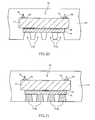
- FIG. 20 shows a method of exposing a part of a metal layer by forming via holes;
- FIG. 21 shows a state that an embedding material is embedded in the via holes;
- FIG. 22 shows a method of exposing a part of a stud bump by forming via holes;
- FIG. 23 shows a method of polishing a resin layer after forming an internal conductive pattern and a resin layer;
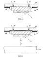
- FIG. 24 shows a semiconductor IC that is positioned and fixed on a transfer substrate;
- FIG. 25 shows a state before pressing a transfer substrate and a prepreg;
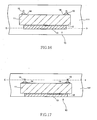
- FIG. 26 shows a state that the transfer substrate is separated after the transfer substrate and the prepreg are pressed;
- FIG. 27 shows a state that the transfer substrate is polished after the transfer substrate and the prepreg are pressed; and
- FIG. 28 shows a state that the transfer substrate is laser-via processed after the transfer substrate and the prepreg are pressed.
- Preferred embodiments of the present invention will now be explained in detail with reference to the drawings.
- FIG. 1 is a schematic cross-sectional view of a configuration of a
semiconductor IC 10 according to a preferred embodiment of the present invention. - As shown in FIG. 1, the
semiconductor IC 10 according to the present embodiment includes: a semiconductor ICmain body 11 on amain surface 11a of which a predetermined circuit (not shown) is formed; an under-barrier metal layer 12 provided at the center of aback surface 11b of the semiconductor ICmain body 11; and ametal layer 13 provided on the under-barrier metal layer 12. - While any types of IC can be used as the
semiconductor IC 10, a digital IC having a very high operation frequency such as a CPU and a DSP can be selectively used. This kind of semiconductor IC generates a large amount of heat by high-speed switching. As described later, thesemiconductor IC 10 according to the present embodiment can dissipate heat to a motherboard remarkably efficiently, even when thesemiconductor IC 10 is embedded in the multilayer substrate. Therefore, a digital IC that generates a large amount of heat can be selected. -
Pad electrodes 14 are formed on themain surface 11a of the semiconductor ICmain body 11. Astud bump 15 as one kind of a conductive projection is formed on each of thepad electrodes 14. In the present invention, it is not essential to form a conductive projection such as thestud pump 15 on thepad electrode 14. However, when the conductive projection is provided, after the semiconductor IC is embedded, the semiconductor IC can be connected to a wiring by forming via holes by emitting a laser beam or by polishing. As described later, thesemiconductor IC 10 can be positioned in the manufacture of a module with embedded semiconductor IC. - The conductive projection is not limited to the
stud bump 15, and various kinds of bumps such as a plate bump, a plated bump, and a ball bump can be used. When a stud bump is used as a conductive projection, silver or copper can be wire bonded to form this stud bump. When a plate bump is used, this can be formed by plating, sputtering, or by deposition. When a plated bump is used, this can be formed by plating. When a ball bump is used, a solder ball is mounted on a land electrode, and is fused to from the ball bump, or a cream solder is printed on a land electrode, and is fused to from the ball bump. - A kind of metal that can be used for the conductive projection is not particularly limited. For example, gold (Au), silver (Ag), copper (Cu), nickel (Ni), tin (Sn), chrome (Cr), nickel chrome alloy (Ni-Cr), and solder can be used. Alternatively, a conductive material is screen printed, and is cured to form a conical or cylindrical bump. Nanopaste can be printed, heated, and sintered to form a bump.
- In the present embodiment, the semiconductor IC
main body 11 has a thickness t (a distance from themain surface 11a to theback surface 11b) smaller than that of a normal semiconductor IC. The thickness t of the semiconductor ICmain body 11 is not particularly limited. Preferably, the thickness t is equal to or smaller than 100 micrometers, for example, about 20 to 50 micrometers. This is because when the thickness t of the semiconductor IC main body is smaller, the total thickness of the module with embedded semiconductor IC can be decreased. - When this thickness t is too small, cracks appear in the semiconductor IC
main body 11, and handling becomes considerably difficult. On the other hand, when the thickness t of the semiconductor ICmain body 11 is set to about 20 to 50 micrometers, occurrence of cracks and remarkable reduction in the easiness of handling can be prevented, while sufficiently decreasing the total thickness of the module with embedded semiconductor IC. - The
semiconductor IC 10 according to the present embodiment has themetal layer 13. Therefore, occurrence of cracks can be prevented more effectively, and easiness of handling is more improved. - The under-
barrier metal layer 12 works to increase close adhesion between the semiconductor ICmain body 11 and themetal layer 13. The urider-barrier metal layer 12 is selectively provided on substantially thewhole back surface 11b of the semiconductor ICmain body 11, excluding theperiphery 11c of theback surface 11b. In the present embodiment, themetal layer 13 is formed by electrolytic plating, as described later. Therefore, the under-barrier metal layer 12 also works as a power supply film. - A material of the under-
barrier metal layer 12 is not particularly limited so long as the material meets the above objects. For example, a material that can be used includes titanium (Ti), chrome (Cr), nickel (Ni), nickel chrome alloy (Ni-Cr), and a laminate of these metals, such as nickel/chrome (Ni/Cr). Furthermore, preferably, the above material is used as a ground material, and copper (Cu) is laminated on this surface, thereby forming the under-barrier metal layer 12. - A film thickness of the under-
barrier metal layer 12 is not particularly limited, and is preferably about 0.05 to 2 micrometers. As an example, when a laminate film (Cr/Cu) of chrome (Cr) and copper (Cu) is used, a thickness of the chrome (Cr) is set to about 0.5 micrometer, and a thickness of the copper (Cu) laminated on this surface is set to about 0.5 micrometer. As described later, the under-barrier metal layer 12 can be formed by sputtering or depositing. The copper (Cu) can be formed on the surface of the ground material by electroless plating. - The
metal layer 13 is formed on the under-barrier metal layer 12 by electroless plating, and is selectively provided on substantially thewhole back surface 11b of the semiconductor ICmain body 11, excluding theperiphery 11c of theback surface 11b. Themetal layer 13 works as a heat dissipation route of heat generated by the operation of the semiconductor ICmain body 11. At the same time, themetal layer 13 works to effectively prevent the occurrence of cracks on theback surface 11b of the semiconductor ICmain body 11, and to improve easiness of handling. - A material of the
metal layer 13 is not particularly limited, so long as the material is a metal that can be formed by plating. For example, the material that can be used includes copper (Cu), silver (Ag), gold (Au), titanium (Ti), chrome (Cr), nickel (Ni), nickel chrome alloy (Ni-Cr), solder, and tin (Sn). Among others, considering cost and thermal conductivity, it is very preferable to use copper (Cu). When copper (Cu) is selected as a material of themetal layer 13, copper sulfate liquid or the like can be used for plating liquid. - While a film thickness of the
metal layer 13 is not particularly limited, the thickness is preferably about 1 to 50 micrometers, and more preferably about 2 to 20 micrometers. Particularly, the thickness of about 5 to 15 micrometers is preferable. This is because when the film thickness of themetal layer 13 is less than one micrometer, effect of crack prevention and effect of improving handling easiness cannot be obtained sufficiently. Furthermore, there is a risk of addition of damage to the semiconductor IC main body, at the time of exposing a part of themetal layer 13 by laser irradiation, after thesemiconductor IC 10 is embedded in a multilayer substrate. - Meanwhile, when a film thickness of the
metal layer 13 exceeds 50 micrometers, a thickness of the module with embedded semiconductor IC manufactured last becomes larger than is necessary. Accordingly, the effect of thinning the semiconductor ICmain body 11 is halved. - On the other hand, when a film thickness of the
metal layer 13 is set to within the above range, the above effect can be sufficiently obtained while decreasing the thickness of the module with embedded semiconductor IC. Furthermore, it becomes possible to decrease the risk of addition of damage to the semiconductor ICmain body 11, at the time of exposing at least a part of themetal layer 13 by laser irradiation, after thesemiconductor IC 10 is embedded in a multilayer substrate. - The configuration of the
semiconductor IC 10 according to the present embodiment is as explained above. A method of manufacturing thesemiconductor IC 10 according to the present embodiment is explained below. - FIG. 2 is a flowchart showing a method of manufacturing the
semiconductor IC 10, and FIG. 3 to FIG. 10 are process diagrams along the flowchart shown in FIG. 2. - First, as shown in FIG. 3, a
back surface 90b of asemiconductor wafer 90 of which front-end process has been completed is polished, that is, a surface opposite to amain surface 90a on which a predetermined circuit such as a transistor is formed is polished, thereby thinning the semiconductor wafer 90 (step S10). However, a method of thinning thesemiconductor wafer 90 is not limited to polishing, and other thinning method, such as etching, plasma treatment, laser irradiation, and blasting can be also used. - Next, a stress-relief processing is performed to the
polished back surface 90b of thesemiconductor wafer 90, thereby relaxing physical stress of theback surface 90b generated by the polishing (step S11). The stress relief processing includes wet etching using an etching liquid, polishing using slurry, dry polishing using a non-diamond abrasive coating, and dry etching using etching gas. - Next, the under-
barrier metal layer 12 is formed on thewhole back surface 90b of thesemiconductor wafer 90 that has been stress-relief processed (step S12). As a method of forming the under-barrier metal layer 12, use of sputtering and deposition is preferable. - As shown in FIG. 4, a resist 91 is formed on the whole surface of the under-barrier metal layer 12 (step S13). Next, as shown in FIG. 5, the resist 91 is patterned by exposing (step S14). Accordingly, a part of the under-
barrier metal layer 12 is covered with the resist 91, and the remaining part of this layer is exposed. The part of the under-barrier metal layer 12 covered with the resist 91 is a region to be disconnected by dicing, and its vicinity. Therefore, the patterned resist 91 forms a grating that separates each semiconductor IC, as shown in a partial top plan view in FIG. 6. - Next, as shown in FIG. 7, the
metal layer 13 is formed on the under-barrier metal layer 12, by electrolytic plating, using the exposed under-barrier metal layer 12 as a power supply film (step S15). Accordingly, themetal layer 13 is selectively formed on the under-barrier metal layer 12. - As shown in FIG. 8, the resist 91 is removed (step S16), and an unnecessary part of the under-
barrier metal layer 12 on which themetal layer 13 is not formed is removed by soft etching, as shown in FIG. 9 (step S17) . Accordingly, theback surface 90b of thesemiconductor wafer 90 is covered with the under-barrier metal layer 12 and themetal layer 13 at the part corresponding to each semiconductor IC, and is exposed in the dicing region and its vicinity. - The
semiconductor wafer 90 is then diced along a line A-A, that is, along the exposed region not covered with the under-barrier metal layer 12 and themetal layer 13, thereby taking out individual semiconductor ICs 10 (step S18). Because the under-barrier metal layer 12 and themetal layer 13 are not formed but thesemiconductor wafer 90 is exposed in the region to be diced, a normal dicer that is optimized to disconnect the semiconductor wafer can be used. - The stud bumps 15 can be formed at any stage, for example, before thinning the semiconductor wafer 90 (step S10). In order to increase adhesion with a resin, preferably, a surface of the
metal layer 13 is roughened, after themetal layer 13 is formed. A roughening method includes intergranular corrosion using hydrogen peroxide/sulfuric acid or formic acid, and tanning. Furthermore, instead of roughening the surface of themetal layer 13, the surface of themetal layer 13 can be rough plated, thereby roughening the surface. - The
semiconductor IC 10 shown in FIG. 1 is then completed in the method as described above. Removing the under-barrier metal layer 12 at step S17 is not essential. That is, dicing can be performed along a line B-B, while leaving the unnecessary part of the under-barrier metal layer 12 on which themetal layer 13 is not formed, as shown in FIG. 10 (step S18). With this arrangement, the soft etching process (step S17) can be omitted. - In this case, the thin under-
barrier metal layer 12 is still present in the area to be diced. Therefore, the dicing condition needs to be different from a normal condition in some cases, to avoid the occurrence of chipping. However, because the under-barrier metal layer 12 has a very small film thickness, the dicing condition of avoiding the chipping is not so strict. - According to the above method, the
metal layer 13 is selectively formed. Therefore, it is possible to avoid warpage that occurs when a thick metal layer is formed on the whole surface of the thinnedsemiconductor wafer 90. The region in which themetal layer 13 is not formed corresponds to a region to be diced. Therefore, the laminate of the semiconductor wafer and the thick metal does not need to be diced. As a result, chipping of the disconnected surface can be effectively prevented. - The above explains the method of manufacturing the
semiconductor IC 10. A semiconductor IC according to other embodiment of the present invention is explained next. - FIG. 11 is a schematic cross-sectional view of a configuration of a
semiconductor IC 20 according to another preferred embodiment of the present invention. - The
semiconductor IC 20 according to the present embodiment is the same as thesemiconductor IC 10 according to the above embodiment, except that thesemiconductor IC 20 includes arust preventing film 21 that covers the back surface. Therefore, identical constituent elements are assigned with like reference numerals, and their redundant explanation is omitted. - The
rust preventing film 21 covers the back surface of thesemiconductor IC 20, that is, the bottom surface and the side surface of thesemiconductor IC 20 on which themetal layer 13 and the under-barrier metal layer 12 are exposed, and also covers theback surface 11b of the semiconductor ICmain body 11 that is exposed at theperiphery 11c. - With this arrangement, the
rust preventing film 21 works to prevent corrosion of themetal layer 13 and to increase close adhesion between the resin and thesemiconductor IC 20. A materia-1 of therust preventing film 21 is not particularly limited so long as the material meets the above objects. For example, the material used includes titanium (Ti), chrome (Cr), nickel (Ni), nickel-chrome alloy (Ni-Cr), and a laminate of these metals, such as nickel/chrome (Ni/Cr). - A film thickness of the
rust preventing film 21 is not particularly limited, and is preferably about 0.005 to 0.5 micrometer. As an example, when chrome (Cr) is used, the film thickness is set to about 0. 05 micrometer. - As explained above, because the
semiconductor IC 20 according to the present embodiment has therust preventing film 21 that covers themetal layer 13, oxidation and corrosion of themetal layer 13 can be effectively prevented, even when a corrosive material such as copper (Cu) is selected for the material of themetal layer 13. As a result, high reliability can be obtained. - As a method of manufacturing the
semiconductor IC 20, a process of forming therust preventing film 21 by sputtering is added to between the process of removing the under-barrier metal layer (step S17) and the process of dicing (step S18). In this case, the dicing is performed in the state that the thinrust preventing film 21 is present in the region to be diced, as explained with reference to FIG. 10. Therefore, the dicing needs to be performed in the condition of not generating chipping. However, since therust preventing film 21 has a very small thickness like the under-barrier metal layer 12, the dicing condition that avoids chipping is not so strict. - In this case, preferably, the surface of the
metal layer 13 is roughened after themetal layer 13 is formed and before therust preventing film 21 is formed. As described above, because therust preventing film 21 has a very small thickness, the roughened surface of themetal layer 13 is reflected to therust preventing film 21. As a result, close adhesion between themetal layer 13 and the resin can be further improved. - In order to securely prevent chipping in the dicing process (step S18), preferably, the
rust preventing film 21 is selectively formed in the region of the semiconductor ICmain body 11, excluding theperiphery 11c. In order to perform this selective formation, ametal mask 92 for covering the region to be disconnected by dicing and its vicinity is used, and selective sputtering or deposition can be performed via anopening 92a of themetal mask 92, as shown in FIG. 12. - As a result, as shown in FIG. 13, the
rust preventing film 21 is formed on substantially the whole surface excluding at least a part not covered by themetal layer 13. Therefore, when thesemiconductor wafer 90 is diced along a line C-C as shown in FIG. 13,individual semiconductor ICs 20 can be easily obtained, without generating chipping. - A module with embedded semiconductor IC that has the
semiconductor IC 10 embedded in a module is explained next. - FIG. 14 a schematic cross-sectional view of a configuration of a module with embedded
semiconductor IC 100 according to a preferred embodiment of the present invention. - As shown in FIG. 14, the module with embedded
semiconductor IC 100 according to the present embodiment includes: amultilayer substrate 110 consisting of laminated resin layers 111 and 112; thesemiconductor IC 10 embedded in themultilayer substrate 110; an internalconductive pattern 120 formed within themultilayer substrate 110; and aheat dissipation electrode 130 provided on abottom surface 110a of themultilayer substrate 110. - The module with embedded
semiconductor IC 100 according to the present embodiment also includes a signal terminal electrode and a power source terminal electrode connected to the internalconductive pattern 120. However, these electrodes are not directly relevant to the gist of the present invention, and are, therefore, not shown in FIG. 14. While thesemiconductor IC 10 shown in FIG. 1 is embedded in the module with embeddedsemiconductor IC 100 according to the present embodiment, thesemiconductor IC 20 shown in FIG. 11 can be also embedded, in place of thesemiconductor IC 10. - In actually use of the module with embedded
semiconductor IC 100, the module with embeddedsemiconductor IC 100 is mounted on a motherboard so that the mounting surface of the motherboard (not shown) faces thebottom surface 110a of themultilayer substrate 110. A ground pattern provided on the mounting surface of the motherboard and aheat dissipation electrode 130 provided on the module with embeddedsemiconductor IC 100 are electrically and mechanically connected to each other. - A material of the resin layers 111 and 112 can be a thermosetting resin or a thermoplastic resin having reflow durability. Specifically, any material can be selected from among an epoxy resin, bismalaimide-triazine resin (BT resin), a phenol resin, a vinyl benzene resin, a polyphenylene ether (polyphenylene etheroxide) resin (PPE, PPO), a cyanate resin, a benzooxyazine resin, a polyimide resin, aromatic polyester resin, polyphenylene sulfide resin, a polyetherimide resin, a polyarilate resin, and a polyetheretherketone resin. A material of unwoven cloth such as glass cloth, aramid, aromatic polyester that is impregnated with one of the above resins can be also used. A material of the above resin that is impregnated with a filler can be also used.
- As explained above, the module with embedded
semiconductor IC 100 according to the present embodiment incorporates the thinnedsemiconductor IC 10. Therefore, the total module with embeddedsemiconductor IC 100 can be thinned. Themetal layer 13 provided on thesemiconductor IC 10 is exposed on thebottom surface 110a of themultilayer substrate 110, and theheat dissipation electrode 130 is directly formed on the exposedmetal layer 13. - Therefore, heat generated by the operation of the
semiconductor IC 10 can be dissipated to the motherboard remarkably efficiently. Consequently, a digital IC having a very high operation frequency such as a CPU and a DSP can be selected for thesemiconductor IC 10. - A method of manufacturing the module with embedded
semiconductor IC 100 is explained next. - FIG. 15 to FIG. 19 are process diagrams sequentially depicting a method of manufacturing the module with embedded
semiconductor IC 100. - First, as shown in FIG. 15, two
prepregs semiconductor IC 10 is pressed by the twoprepregs semiconductor IC 10 is heated while being pressed by theprepregs prepregs resin layer 111 is formed as shown in FIG. 16. Thesemiconductor IC 10 is embedded in theresin layer 111. - Next, the bottom surface of the
resin layer 111 embedded with thesemiconductor IC 10 is polished, thereby removing a part of theresin layer 111 up to a line D-D shown in FIG. 16. As a result, themetal layer 13 of thesemiconductor IC 10 is exposed, and the bottom surface of theresin layer 111 forms substantially the same plane as the front surface of themetal layer 13. - The upper surface of the
resin layer 111 is then polished, thereby removing a part of theresin layer 111 up to a line E-E shown in FIG. 17, and exposing a part of the stud bumps 15 of thesemiconductor IC 10 as show in FIG. 18. - As shown in FIG. 19, the internal
conductive layer 120 is formed to be connected to the exposedstud bump 15, and theresin layer 112 that covers the internalconductive layer 120 is formed. Furthermore, theheat dissipation electrode 130 is formed, thereby completing the module with embeddedsemiconductor IC 100 shown in FIG. 14. - When the module with embedded
semiconductor IC 100 is manufactured in the above method, substantially the whole surface of themetal layer 13 can be exposed. Therefore, a configuration having remarkably high heat dissipation can be obtained. In this case, when themetal layer 13 has a smaller thickness, high precision is required to adjust the amount of polishing theresin layer 111. When themetal layer 13 has a certain level of thickness (preferably equal to or larger than 5 micrometers), higher precision is not required to adjust the amount of polishing, and polishing can be performed easily. - According to the above manufacturing method, the
metal layer 13 of thesemiconductor IC 10 is exposed by polishing the bottom surface of theresin layer 111. The method of exposing themetal layer 13 is not limited to this. - As shown in FIG. 20, via
holes 111c can be formed in theresin layer 111, by irradiating a laser beam, thereby exposing a part of themetal layer 13. In this case, as shown in FIG. 21, amaterial 111d having higher thermal conductivity than that of theresin layer 111 is embedded in the viaholes 111c, and theheat dissipation electrode 130 is formed on the surface of the embeddedmaterial 111d. When the thickness of themetal layer 13 is too small, there is a risk that thesemiconductor wafer 90 is directly damaged by energy of the irradiated laser beam, and the circuit such as the transistor formed on thesemiconductor IC 10 is damaged. However, when themetal layer 13 has a certain level of thickness (preferably equal to or larger than 5 micrometers), occurrence of this damage can be prevented. - Either one of or both a metal and a conductive adhesive can be used for the embedded
material 111d. When metal is used for the embeddedmaterial 111d, this can be formed by plating. Preferably, the embeddedmaterial 111d is completely filled. Plating and a conductive or insulating paste can be used together, or a conductive adhesive can be used. - In this case, the embedded
material 111d can be formed by screen printing. When plating and a conductive or insulating paste are used together, the sidewall of the viaholes 111c is covered with metal, and the inside is filled with the conductive or insulating paste. When the conductive or insulating paste is used, the paste preferably contains a filler to increase thermal conductivity. - Furthermore, according to the above manufacturing method, the stud bumps 15 of the
semiconductor IC 10 are exposed by polishing the upper surface of theresin layer 111. Alternatively, as shown in FIG. 22, viaholes 111e can be formed in theresin layer 111 by irradiating a laser beam, thereby exposing a part of a conductive projection such as the stud bumps 15. - Furthermore, according to the above manufacturing method, the bottom surface of the
resin layer 111 is polished to expose themetal layer 13 of thesemiconductor IC 10. Thereafter, the internalconductive pattern 120 is formed, and theresin layer 112 is formed to cover the internalconductive pattern 120. Alternatively, as shown in FIG. 23, after the internalconductive pattern 120 and theresin layer 112 are formed, a part of thesemiconductor IC 100 up to a line F-F can be removed by polishing. - When the pitch of the
pad electrodes 14 provided on thesemiconductor IC 10 is very small, for example, when the pitch is equal to or smaller than 100 micrometers, particularly about 60 micrometers, high precision is required in the positioning of thepad electrodes 14 and the internalconductive pattern 120. In this case, it is effective to perform positioning using conductive projections such as the stud bumps 15 provided on thepad electrodes 14. - For example, as shown in FIG. 24, a
transfer plate 190 formed withpositioning holes 191 and an internalconductive pattern 120 is prepared in advance. Anadhesive sheet 200 is laminated on this. The stud bumps 15 of thesemiconductor IC 10 are engaged with the positioning holes 191, and are provisionally stopped. In this state, as shown in FIG. 25, theprepreg 111a and thetransfer substrate 190 are pressed, and thetransfer substrate 190 is peeled off. - As shown in FIG. 26, the internal
conductive pattern 120 and thesemiconductor IC 10 are embedded in theresin layer 111. Alternatively, instead of peeling off thetransfer substrate 190, thetransfer substrate 190 is polished, after the internalconductive pattern 120 and thesemiconductor IC 10 are embedded, thereby exposing the stud bumps 15, as shown in FIG. 27. - Alternatively, after the internal
conductive pattern 120 and thesemiconductor IC 10 are embedded, thetransfer substrate 190 is irradiated with a laser beam to form via holes, thereby exposing the stud bumps 15, as shown in FIG. 28. In this case, a positional relationship between the internalconductive pattern 120 and the stud bumps 15 of thesemiconductor IC 10 is prescribed by thetransfer substrate 190. Therefore, no positional deviation occurs between the internalconductive pattern 120 and the stud bumps 15 of thesemiconductor IC 10. Consequently, even when the pitch of thepad electrodes 14 provided on thesemiconductor IC 10 is very small, it becomes possible to prevent the occurrence of a positional deviation between the stud bumps 15 and the internalconductive pattern 120. - Thereafter, as shown in FIG. 17, substantially the whole surface of the
metal layer 13 of thesemiconductor IC 10 is exposed by polishing. Alternatively, as shown in FIG. 20, the viaholes 111c are formed in theresin layer 111 by irradiating a laser beam, thereby exposing a part of themetal layer 13. At the same time, other internalconductive pattern 120 and theresin layer 112 are formed, and bumps of theheat dissipation electrode 130 are formed, thereby completing the module with embedded semiconductor IC. - As explained above, the module with embedded
semiconductor IC 100 according to the present embodiment incorporates the thinnedsemiconductor IC 10, and can dissipate, remarkably efficiently, heat generated by the operation of thesemiconductor IC 10, to the motherboard. Therefore, the invention can provide a thin module embedded with a digital IC having a very high operation frequency such as a CPU and a DSP. - Because the
back surface 11b of the semiconductor ICmain body 11 is protected by themetal layer 13, a crack is not easily generated in the semiconductor ICmain body 11, despite a heat shock during the press process and the manufacturing process, a heat shock after a completion of the product, or during a reliability test of reflow and a mechanical stress test such as a bending test. Consequently, high reliability can be obtained. - As explained above, the semiconductor IC according to the present invention can obtain high thermal conductivity, even when the semiconductor IC is embedded in a circuit board made of resin.
Therefore, the present can be very suitably applied to a semiconductor IC having high heat generation such as a CPU and a DSP. Because a metal layer is selectively provided, warpage does not occur in the wafer state, even when the semiconductor IC main body is thinned by polishing. Accordingly, the semiconductor IC can be manufactured easily. - Because the metal layer is provided at the center of the back surface of the semiconductor IC main body, a laminate of the semiconductor wafer and the thick metal does not need to be diced. As a result, chipping of the disconnected surface can be prevented effectively. Consequently, a thin module with embedded semiconductor IC having high heat dissipation can be manufactured, by embedding this semiconductor IC in a multilayer substrate.
- The present invention is in no way limited to the aforementioned embodiments, but rather various modifications are possible within the scope of the invention as recited in the claims, and naturally these modifications are included within the scope of the invention.
Claims (18)
- A semiconductor integrated circuit, comprising:a main body that a predetermined circuit is formed on a main surface thereof; anda metal layer selectively provided at a center of a back surface of the main body.
- The semiconductor integrated circuit as claimed in claim 1, wherein said metal layer is provided on substantially the whole back surface of the main body except a periphery of the back surface.
- The semiconductor integrated circuit as claimed in claim 1 or 2, further comprising an under-barrier metal layer provided between at least the metal layer and the back surface of the main body.
- The semiconductor integrated circuit as claimed in any one of claims 1 to 3, further comprising a rust preventing film that covers a bottom surface and a side surface of the metal layer.
- The semiconductor integrated circuit as claimed in claim 4, wherein said rust preventing film is selectively provided in a region of the back surface of the main body except a periphery of the back surface.
- The semiconductor integrated circuit as claimed in any one of claims 1 to 5, wherein said main body is thinned.
- A method of manufacturing a semiconductor integrated circuit, comprising:a first step for selectively forming a metal layer on a back surface of a semiconductor wafer that a predetermined circuit is formed on a main surface thereof; anda second step for disconnecting the semiconductor wafer along a region in which the metal layer is not formed.
- The method of manufacturing a semiconductor integrated circuit as claimed in claim 7, wherein said first step includes:a step for forming an under-barrier metal layer on substantially the whole back surface of the semiconductor wafer; anda step for selectively forming the metal layer on the under-barrier metal layer by plating while covering a part of the under-barrier metal layer with a resist.
- The method of manufacturing a semiconductor integrated circuit as claimed in claim 8, wherein said first step further includes:a step for removing the resist after selectively forming the metal layer; anda step for removing the under-barrier metal layer exposed by removing the resist.
- The method of manufacturing a semiconductor integrated circuit as claimed in any one of claims 7 to 9, further comprising a step for thinning the semiconductor wafer before performing the first step.
- The method of manufacturing a semiconductor integrated circuit as claimed in any one of claims 7 to 10, further comprising a step for forming a rust preventing film that covers a bottom surface and a side surface of the metal layer after performing the first step and before performing the second step.
- The method of manufacturing a semiconductor integrated circuit as claimed in claim 11, wherein said step for forming the rust preventing film is performed by selectively forming the rust preventing film on substantially the whole back surface of the semiconductor wafer, except at least a part of a region of the back surface not covered with the metal layer.
- The method of manufacturing a semiconductor integrated circuit as claimed in any one of claims 7 to 12, further comprising a step for roughening a surface of the metal layer.
- A module with embedded semiconductor integrated circuit, comprising:a semiconductor integrated circuit including a main body that a predetermined circuit is formed on a main surface thereof and a metal layer selectively provided at a center of a back surface of the main body; anda resin layer into which the semiconductor IC is embedded.
- A method of manufacturing a module with embedded semiconductor integrated circuit, comprising:a first step for embedding a semiconductor integrated circuit including a main body that a predetermined circuit is formed on a main surface thereof and a metal layer selectively provided at a center of a back surface of the main body; anda second step for exposing at least a part of a surface of the metal layer.
- The method of manufacturing a module with embedded semiconductor integrated circuit as claimed in claim 15, wherein said second step is performed by exposing substantially a whole bottom surface of the metal layer by polishing a bottom surface of the resin layer.
- The method of manufacturing a module with embedded semiconductor integrated circuit as claimed in claim 15, wherein said second step is performed by exposing at least a part of a bottom surface of the metal layer by forming via holes on a bottom surface of the resin layer.
- The method of manufacturing a module with embedded semiconductor integrated circuit as claimed in claim 17, further comprising a third step for embedding the via holes with a material having higher thermal conductivity than that of the resin layer.
Applications Claiming Priority (1)
| Application Number | Priority Date | Filing Date | Title |
|---|---|---|---|
| JP2005161414A JP2006339354A (en) | 2005-06-01 | 2005-06-01 | SEMICONDUCTOR IC AND ITS MANUFACTURING METHOD, SEMICONDUCTOR IC BUILT-IN MODULE, AND ITS MANUFACTURING METHOD |
Publications (2)
| Publication Number | Publication Date |
|---|---|
| EP1729341A2 true EP1729341A2 (en) | 2006-12-06 |
| EP1729341A3 EP1729341A3 (en) | 2014-03-26 |
Family
ID=36986842
Family Applications (1)
| Application Number | Title | Priority Date | Filing Date |
|---|---|---|---|
| EP06252853.4A Withdrawn EP1729341A3 (en) | 2005-06-01 | 2006-06-01 | Semiconductor IC and its manufacturing method, and module with embedded semiconductor IC and its manufacturing method |
Country Status (5)
| Country | Link |
|---|---|
| US (2) | US20060273451A1 (en) |
| EP (1) | EP1729341A3 (en) |
| JP (1) | JP2006339354A (en) |
| KR (1) | KR20060125602A (en) |
| CN (1) | CN1873980A (en) |
Cited By (2)
| Publication number | Priority date | Publication date | Assignee | Title |
|---|---|---|---|---|
| EP2168154A4 (en) * | 2007-07-12 | 2012-07-11 | Vishay Gen Semiconductor Llc | UNDER ASSEMBLY COMPRISING A POWER SEMICONDUCTOR CHIP AND A THERMAL DISSIPATOR HAVING A SURFACE PORTION EXPOSED THEREFROM |
| EP2168144A4 (en) * | 2007-07-12 | 2012-07-25 | Vishay Gen Semiconductor Llc | SUBASSEMBLY WHICH COMPRISES A POWER SEMICONDUCTOR CHIP AND A HEAT WELL AND METHOD OF FORMING THE SAME |
Families Citing this family (16)
| Publication number | Priority date | Publication date | Assignee | Title |
|---|---|---|---|---|
| JP2010073809A (en) * | 2008-09-17 | 2010-04-02 | Tdk Corp | Method of manufacturing printed circuit board |
| US8450151B1 (en) * | 2011-11-22 | 2013-05-28 | Texas Instruments Incorporated | Micro surface mount device packaging |
| US20130127044A1 (en) * | 2011-11-22 | 2013-05-23 | Texas Instruments Incorporated | Micro surface mount device packaging |
| US9673162B2 (en) * | 2012-09-13 | 2017-06-06 | Nxp Usa, Inc. | High power semiconductor package subsystems |
| US10566267B2 (en) | 2017-10-05 | 2020-02-18 | Texas Instruments Incorporated | Die attach surface copper layer with protective layer for microelectronic devices |
| CN118263196B (en) * | 2017-12-20 | 2026-01-30 | 安世有限公司 | Chip-scale packaged semiconductor devices and their manufacturing methods |
| US11114402B2 (en) * | 2018-02-23 | 2021-09-07 | Semiconductor Components Industries, Llc | Semiconductor device with backmetal and related methods |
| CN109473405A (en) * | 2018-12-07 | 2019-03-15 | 华进半导体封装先导技术研发中心有限公司 | A fan-out wafer-level packaging structure with silicon etched through holes and method thereof |
| US11277917B2 (en) | 2019-03-12 | 2022-03-15 | Advanced Semiconductor Engineering, Inc. | Embedded component package structure, embedded type panel substrate and manufacturing method thereof |
| US10950551B2 (en) | 2019-04-29 | 2021-03-16 | Advanced Semiconductor Engineering, Inc. | Embedded component package structure and manufacturing method thereof |
| US11296030B2 (en) | 2019-04-29 | 2022-04-05 | Advanced Semiconductor Engineering, Inc. | Embedded component package structure and manufacturing method thereof |
| DE102019116928B3 (en) | 2019-06-24 | 2020-12-10 | Infineon Technologies Ag | DIE HOUSING AND METHOD OF MANUFACTURING A DIE HOUSING |
| JP7363158B2 (en) * | 2019-07-24 | 2023-10-18 | Tdk株式会社 | Electronic component built-in board and manufacturing method thereof |
| TW202245020A (en) * | 2021-05-12 | 2022-11-16 | 宜錦科技股份有限公司 | Wafer backside structure and manufacture method thereof |
| US12532741B2 (en) * | 2022-11-11 | 2026-01-20 | Amkor Technology Singapore Holding Pte. Ltd. | Semiconductor devices and methods of manufacturing semiconductor devices |
| CN118841334B (en) * | 2024-09-20 | 2024-12-10 | 渠梁电子有限公司 | A method for manufacturing a semi-finished wafer and a semi-finished wafer |
Citations (3)
| Publication number | Priority date | Publication date | Assignee | Title |
|---|---|---|---|---|
| JPH09321408A (en) | 1996-05-31 | 1997-12-12 | Nec Corp | High density mounting structure of electronic circuit board |
| JP2003174116A (en) | 2001-09-25 | 2003-06-20 | Toshiba Corp | Method for manufacturing semiconductor device |
| JP2005064470A (en) | 2003-07-30 | 2005-03-10 | Tdk Corp | Semiconductor IC built-in module and manufacturing method thereof |
Family Cites Families (18)
| Publication number | Priority date | Publication date | Assignee | Title |
|---|---|---|---|---|
| JPS62274755A (en) * | 1986-05-23 | 1987-11-28 | Hitachi Vlsi Eng Corp | Semiconductor device |
| JPS63106130U (en) * | 1986-12-26 | 1988-07-08 | ||
| JPH0740600B2 (en) * | 1987-04-30 | 1995-05-01 | 三菱電機株式会社 | Semiconductor device |
| JPH0465147A (en) * | 1990-07-05 | 1992-03-02 | Fujitsu Ltd | Manufacture apparatus of semiconductor device |
| JP2984068B2 (en) * | 1991-01-31 | 1999-11-29 | 株式会社日立製作所 | Method for manufacturing semiconductor device |
| JPH04315446A (en) * | 1991-04-15 | 1992-11-06 | Hitachi Ltd | Semiconductor wafer and semiconductor integrated device using same |
| US5596231A (en) * | 1991-08-05 | 1997-01-21 | Asat, Limited | High power dissipation plastic encapsulated package for integrated circuit die |
| JPH06268112A (en) * | 1993-03-10 | 1994-09-22 | Mitsubishi Electric Corp | Semiconductor device and manufacturing method thereof |
| JPH0758254A (en) * | 1993-08-19 | 1995-03-03 | Fujitsu Ltd | Multi-chip module and manufacturing method thereof |
| JPH0766332A (en) * | 1993-08-25 | 1995-03-10 | Seiko Epson Corp | Semiconductor device |
| KR0185512B1 (en) * | 1996-08-19 | 1999-03-20 | 김광호 | Column lead type package and method of making the same |
| JP2001110831A (en) * | 1999-10-07 | 2001-04-20 | Seiko Epson Corp | External connection projection and method of forming the same, semiconductor chip, circuit board, and electronic device |
| JP3537400B2 (en) * | 2000-03-17 | 2004-06-14 | 松下電器産業株式会社 | Semiconductor built-in module and method of manufacturing the same |
| JP3520039B2 (en) * | 2000-10-05 | 2004-04-19 | 三洋電機株式会社 | Semiconductor device and semiconductor module |
| JP4093826B2 (en) * | 2002-08-27 | 2008-06-04 | 富士通株式会社 | Clock generator |
| JP3595323B2 (en) * | 2002-11-22 | 2004-12-02 | 沖電気工業株式会社 | Semiconductor device and manufacturing method thereof |
| JP2004327624A (en) * | 2003-04-23 | 2004-11-18 | Shinko Electric Ind Co Ltd | Multi-layer circuit board with built-in components |
| US7362580B2 (en) * | 2004-06-18 | 2008-04-22 | Intel Corporation | Electronic assembly having an indium wetting layer on a thermally conductive body |
-
2005
- 2005-06-01 JP JP2005161414A patent/JP2006339354A/en active Pending
-
2006
- 2006-05-31 US US11/445,082 patent/US20060273451A1/en not_active Abandoned
- 2006-06-01 EP EP06252853.4A patent/EP1729341A3/en not_active Withdrawn
- 2006-06-01 KR KR1020060049606A patent/KR20060125602A/en not_active Withdrawn
- 2006-06-01 CN CNA2006100885212A patent/CN1873980A/en active Pending
-
2010
- 2010-01-23 US US12/692,602 patent/US20100178737A1/en not_active Abandoned
Patent Citations (3)
| Publication number | Priority date | Publication date | Assignee | Title |
|---|---|---|---|---|
| JPH09321408A (en) | 1996-05-31 | 1997-12-12 | Nec Corp | High density mounting structure of electronic circuit board |
| JP2003174116A (en) | 2001-09-25 | 2003-06-20 | Toshiba Corp | Method for manufacturing semiconductor device |
| JP2005064470A (en) | 2003-07-30 | 2005-03-10 | Tdk Corp | Semiconductor IC built-in module and manufacturing method thereof |
Cited By (3)
| Publication number | Priority date | Publication date | Assignee | Title |
|---|---|---|---|---|
| EP2168154A4 (en) * | 2007-07-12 | 2012-07-11 | Vishay Gen Semiconductor Llc | UNDER ASSEMBLY COMPRISING A POWER SEMICONDUCTOR CHIP AND A THERMAL DISSIPATOR HAVING A SURFACE PORTION EXPOSED THEREFROM |
| EP2168144A4 (en) * | 2007-07-12 | 2012-07-25 | Vishay Gen Semiconductor Llc | SUBASSEMBLY WHICH COMPRISES A POWER SEMICONDUCTOR CHIP AND A HEAT WELL AND METHOD OF FORMING THE SAME |
| US8252633B2 (en) | 2007-07-12 | 2012-08-28 | Vishay General Semiconductor Llc | Subassembly that includes a power semiconductor die and a heat sink having an exposed surface portion thereof |
Also Published As
| Publication number | Publication date |
|---|---|
| KR20060125602A (en) | 2006-12-06 |
| US20060273451A1 (en) | 2006-12-07 |
| EP1729341A3 (en) | 2014-03-26 |
| CN1873980A (en) | 2006-12-06 |
| US20100178737A1 (en) | 2010-07-15 |
| JP2006339354A (en) | 2006-12-14 |
Similar Documents
| Publication | Publication Date | Title |
|---|---|---|
| US20100178737A1 (en) | Semiconductor IC and Its Manufacturing Method, and Module with Embedded Semiconductor IC and Its Manufacturing Method | |
| CN1941339B (en) | Semiconductor IC-embedded substrate and method for manufacturing same | |
| JP4835124B2 (en) | Semiconductor IC-embedded substrate and manufacturing method thereof | |
| US7547975B2 (en) | Module with embedded semiconductor IC and method of fabricating the module | |
| KR101084924B1 (en) | Semiconductor device and manufacturing method thereof | |
| JP3938921B2 (en) | Manufacturing method of semiconductor IC built-in module | |
| JP2015159197A (en) | Wiring board and method for manufacturing the same | |
| US8766101B2 (en) | Wiring substrate, method for manufacturing wiring substrate, and semiconductor package including wiring substrate | |
| US7829378B2 (en) | Method of manufacturing electronic device, substrate and semiconductor device | |
| CN105304580B (en) | Semiconductor device and manufacturing method thereof | |
| US7964493B2 (en) | Method of manufacturing semiconductor device | |
| JP4121543B1 (en) | Electronic equipment | |
| US7045393B2 (en) | Method for manufacturing circuit devices | |
| KR20080036925A (en) | Semiconductor device and manufacturing method thereof | |
| JP2005353837A (en) | Semiconductor device and manufacturing method thereof | |
| US20100112786A1 (en) | Method of manufacturing semiconductor device | |
| JP4679000B2 (en) | Plate | |
| JP2020129637A (en) | Electronic device and manufacturing method thereof | |
| JP4663172B2 (en) | Manufacturing method of semiconductor device | |
| JP5479214B2 (en) | Manufacturing method of light emitting element mounting substrate | |
| JP2018056445A (en) | Wiring board with carrier base material and method for manufacturing wiring board with carrier base material | |
| JP2003037345A (en) | Circuit device and method of manufacturing the same | |
| JP2006049822A (en) | Module with built-in semiconductor IC | |
| JP4286264B2 (en) | Semiconductor device and manufacturing method thereof | |
| JPH06112353A (en) | Manufacturing method of leaded substrate for semiconductor mounting |
Legal Events
| Date | Code | Title | Description |
|---|---|---|---|
| PUAI | Public reference made under article 153(3) epc to a published international application that has entered the european phase |
Free format text: ORIGINAL CODE: 0009012 |
|
| AK | Designated contracting states |
Kind code of ref document: A2 Designated state(s): AT BE BG CH CY CZ DE DK EE ES FI FR GB GR HU IE IS IT LI LT LU LV MC NL PL PT RO SE SI SK TR |
|
| AX | Request for extension of the european patent |
Extension state: AL BA HR MK YU |
|
| RAP1 | Party data changed (applicant data changed or rights of an application transferred) |
Owner name: TDK CORPORATION |
|
| PUAL | Search report despatched |
Free format text: ORIGINAL CODE: 0009013 |
|
| AK | Designated contracting states |
Kind code of ref document: A3 Designated state(s): AT BE BG CH CY CZ DE DK EE ES FI FR GB GR HU IE IS IT LI LT LU LV MC NL PL PT RO SE SI SK TR |
|
| AX | Request for extension of the european patent |
Extension state: AL BA HR MK YU |
|
| RIC1 | Information provided on ipc code assigned before grant |
Ipc: H01L 23/433 20060101ALI20140214BHEP Ipc: H01L 23/00 20060101ALI20140214BHEP Ipc: H01L 23/31 20060101AFI20140214BHEP |
|
| AKX | Designation fees paid |
Designated state(s): AT BE BG CH CY CZ DE DK EE ES FI FR GB GR HU IE IS IT LI LT LU LV MC NL PL PT RO SE SI SK TR |
|
| STAA | Information on the status of an ep patent application or granted ep patent |
Free format text: STATUS: THE APPLICATION IS DEEMED TO BE WITHDRAWN |
|
| 18D | Application deemed to be withdrawn |
Effective date: 20140927 |