JP3938921B2 - Manufacturing method of semiconductor IC built-in module - Google Patents
Manufacturing method of semiconductor IC built-in module Download PDFInfo
- Publication number
- JP3938921B2 JP3938921B2 JP2004191369A JP2004191369A JP3938921B2 JP 3938921 B2 JP3938921 B2 JP 3938921B2 JP 2004191369 A JP2004191369 A JP 2004191369A JP 2004191369 A JP2004191369 A JP 2004191369A JP 3938921 B2 JP3938921 B2 JP 3938921B2
- Authority
- JP
- Japan
- Prior art keywords
- semiconductor
- built
- module
- transfer substrate
- resin layer
- Prior art date
- Legal status (The legal status is an assumption and is not a legal conclusion. Google has not performed a legal analysis and makes no representation as to the accuracy of the status listed.)
- Active
Links
Images


Classifications
-
- H—ELECTRICITY
- H01—ELECTRIC ELEMENTS
- H01L—SEMICONDUCTOR DEVICES NOT COVERED BY CLASS H10
- H01L24/00—Arrangements for connecting or disconnecting semiconductor or solid-state bodies; Methods or apparatus related thereto
- H01L24/01—Means for bonding being attached to, or being formed on, the surface to be connected, e.g. chip-to-package, die-attach, "first-level" interconnects; Manufacturing methods related thereto
- H01L24/18—High density interconnect [HDI] connectors; Manufacturing methods related thereto
- H01L24/19—Manufacturing methods of high density interconnect preforms
-
- H—ELECTRICITY
- H01—ELECTRIC ELEMENTS
- H01L—SEMICONDUCTOR DEVICES NOT COVERED BY CLASS H10
- H01L21/00—Processes or apparatus adapted for the manufacture or treatment of semiconductor or solid state devices or of parts thereof
- H01L21/02—Manufacture or treatment of semiconductor devices or of parts thereof
- H01L21/04—Manufacture or treatment of semiconductor devices or of parts thereof the devices having at least one potential-jump barrier or surface barrier, e.g. PN junction, depletion layer or carrier concentration layer
- H01L21/50—Assembly of semiconductor devices using processes or apparatus not provided for in a single one of the subgroups H01L21/06 - H01L21/326, e.g. sealing of a cap to a base of a container
- H01L21/56—Encapsulations, e.g. encapsulation layers, coatings
- H01L21/568—Temporary substrate used as encapsulation process aid
-
- H—ELECTRICITY
- H01—ELECTRIC ELEMENTS
- H01L—SEMICONDUCTOR DEVICES NOT COVERED BY CLASS H10
- H01L2224/00—Indexing scheme for arrangements for connecting or disconnecting semiconductor or solid-state bodies and methods related thereto as covered by H01L24/00
- H01L2224/01—Means for bonding being attached to, or being formed on, the surface to be connected, e.g. chip-to-package, die-attach, "first-level" interconnects; Manufacturing methods related thereto
- H01L2224/02—Bonding areas; Manufacturing methods related thereto
- H01L2224/04—Structure, shape, material or disposition of the bonding areas prior to the connecting process
- H01L2224/04105—Bonding areas formed on an encapsulation of the semiconductor or solid-state body, e.g. bonding areas on chip-scale packages
-
- H—ELECTRICITY
- H01—ELECTRIC ELEMENTS
- H01L—SEMICONDUCTOR DEVICES NOT COVERED BY CLASS H10
- H01L2224/00—Indexing scheme for arrangements for connecting or disconnecting semiconductor or solid-state bodies and methods related thereto as covered by H01L24/00
- H01L2224/01—Means for bonding being attached to, or being formed on, the surface to be connected, e.g. chip-to-package, die-attach, "first-level" interconnects; Manufacturing methods related thereto
- H01L2224/18—High density interconnect [HDI] connectors; Manufacturing methods related thereto
- H01L2224/19—Manufacturing methods of high density interconnect preforms
-
- H—ELECTRICITY
- H01—ELECTRIC ELEMENTS
- H01L—SEMICONDUCTOR DEVICES NOT COVERED BY CLASS H10
- H01L2924/00—Indexing scheme for arrangements or methods for connecting or disconnecting semiconductor or solid-state bodies as covered by H01L24/00
- H01L2924/10—Details of semiconductor or other solid state devices to be connected
- H01L2924/11—Device type
- H01L2924/14—Integrated circuits
Description
本発明は半導体IC内蔵モジュール及びその製造方法に関し、特に、電極ピッチが狭い半導体ICを内蔵するのに好適な半導体IC内蔵モジュール及びその製造方法に関する。 The present invention relates to a semiconductor IC built-in module and a manufacturing method thereof, and more particularly to a semiconductor IC built-in module suitable for incorporating a semiconductor IC having a narrow electrode pitch and a manufacturing method thereof.
近年、半導体IC搭載モジュールに対する小型化・薄型化の要求を満たすべく、搭載する半導体ICをベアチップの状態でプリント基板に搭載する提案が数多くなされている。ベアチップ状態の半導体ICは、パッケージングされた半導体ICに比べて電極ピッチが非常に狭いことから、これをプリント基板に搭載する場合、半導体ICに設けられた電極(以下、「ランド電極」という)とプリント基板に設けられた配線(以下、「基板配線パターン」という)との接続をどのようにして行うかが重要な問題となる。 In recent years, many proposals have been made to mount a semiconductor IC to be mounted on a printed circuit board in a bare chip state in order to satisfy the demand for miniaturization and thinning of a semiconductor IC mounting module. A bare chip semiconductor IC has a very narrow electrode pitch compared to a packaged semiconductor IC. Therefore, when the semiconductor IC is mounted on a printed circuit board, an electrode provided on the semiconductor IC (hereinafter referred to as a “land electrode”). It is an important problem how to connect the wiring to the wiring (hereinafter referred to as “substrate wiring pattern”) provided on the printed circuit board.
ランド電極と基板配線パターンとを接続する一つの方法として、ワイヤボンディングによりこれらを接続する方法が知られている。この方法によれば、ベアチップ状態の半導体ICを比較的容易に実装可能であるものの、半導体ICを搭載する領域とボンディングワイヤを接続する領域とをプリント基板上の別平面とする必要があることから、実装面積が大きくなるという問題があった。 As one method for connecting the land electrode and the substrate wiring pattern, a method for connecting them by wire bonding is known. According to this method, a semiconductor IC in a bare chip state can be mounted relatively easily, but the area for mounting the semiconductor IC and the area for connecting the bonding wires need to be provided on different planes on the printed circuit board. There is a problem that the mounting area becomes large.
また、ランド電極と基板配線パターンとを接続する他の方法として、ベアチップ状態の半導体ICをプリント基板にフリップチップ接続する方法も知られている。この方法によれば、実装面積を小さくすることが可能であるものの、ランド電極と基板配線パターンとの機械的な接続強度を十分に確保するためには、ランド電極の表面に多層のアンダーバリアメタルを施す必要があるなど、工程が複雑になるという問題があった。 As another method of connecting the land electrode and the substrate wiring pattern, a method of flip chip connecting a bare-chip semiconductor IC to a printed circuit board is also known. Although it is possible to reduce the mounting area according to this method, in order to ensure sufficient mechanical connection strength between the land electrode and the substrate wiring pattern, a multilayer under barrier metal is formed on the surface of the land electrode. There is a problem that the process becomes complicated.
しかも、上述した2つの方法は、いずれもプリント基板の表面に半導体ICを搭載するものであることから、モジュール全体を薄くすることが困難であるという共通の問題があった。これを解決する方法としては、特許文献1に記載されているように、プリント基板にキャビティを形成してその内部にベアチップ状態の半導体ICを埋め込み、これにより半導体IC内蔵モジュールを構成する方法が考えられる。
In addition, since the two methods described above both mount a semiconductor IC on the surface of the printed board, there is a common problem that it is difficult to make the entire module thin. As a method for solving this, as described in
しかしながら、特許文献1に記載された方法では、キャビティが形成された部分の強度を確保するためにプリント基板の厚さをある程度厚くする必要があり、これがモジュールの薄型化の妨げになるという問題があった。さらに、キャビティの平面方向の大きさを半導体ICの平面の方向の大きさよりもある程度大きく設定する必要があることから、ランド電極と基板配線パターンとの相対的な位置関係にずれが生じ、このため電極ピッチが100μm以下といった狭い半導体ICを用いることは非常に困難であった。
このように、従来の半導体IC内蔵モジュールでは、十分な薄型化が困難であると同時に、電極ピッチが狭い半導体ICを用いることは非常に困難であった。 As described above, in the conventional semiconductor IC built-in module, it is difficult to sufficiently reduce the thickness, and at the same time, it is very difficult to use a semiconductor IC having a narrow electrode pitch.
したがって、本発明の目的は、いっそうの薄型化を実現可能な半導体IC内蔵モジュール及びその製造方法を提供することである。 Accordingly, an object of the present invention is to provide a module with a built-in semiconductor IC capable of realizing further reduction in thickness and a method for manufacturing the same.
また、本発明の他の目的は、電極ピッチが非常に狭い半導体ICを用いることが可能な半導体IC内蔵モジュール及びその製造方法を提供することである。 Another object of the present invention is to provide a semiconductor IC built-in module capable of using a semiconductor IC with a very narrow electrode pitch and a method for manufacturing the same.
本発明による半導体IC内蔵モジュールは、第1の樹脂層と、第2の樹脂層と、少なくとも前記第1及び第2の樹脂層内に埋め込まれたポスト電極と、前記第1の樹脂層と前記第2の樹脂層との間に埋め込まれるように固定された半導体ICとを備え、前記半導体ICのランド電極上にはバンプが設けられ、前記バンプは前記ポスト電極に対して位置決めされていることを特徴とする。また、本発明による半導体IC内蔵モジュールは、第1の樹脂層と、第2の樹脂層と、前記第1及び第2の樹脂層を貫通して設けられたポスト電極と、前記第1の樹脂層と前記第2の樹脂層との間に埋め込まれるように固定され、薄膜化された半導体ICとを備え、前記半導体ICのランド電極上にはバンプが設けられ、前記バンプは前記ポスト電極に対して位置決めされていることを特徴とする。 A semiconductor IC built-in module according to the present invention includes a first resin layer, a second resin layer, at least a post electrode embedded in the first and second resin layers, the first resin layer, and the and a fixed semiconductor IC to be embedded between the second resin layer, said on the land electrodes of the semiconductor IC bumps provided, said bumps being positioned with respect to the post electrode It is characterized by. The module with a built-in semiconductor IC according to the present invention includes a first resin layer, a second resin layer, a post electrode provided through the first and second resin layers, and the first resin. is fixed so as to be buried between the the layer second resin layer, and a semiconductor IC that is thinned, bumps provided on the land electrodes of the semiconductor IC, the bumps in the post electrode It is characterized by being positioned with respect to.
本発明によれば、第1の樹脂層と第2の樹脂層との間に半導体ICが埋め込まれていることから、半導体IC内蔵モジュール全体の厚さを薄くすることが可能となる。しかも、半導体ICに設けられたバンプがポスト電極に対して位置決めされていることから、バンプの平面的な位置が実質的に固定的となり、したがって、100μm以下、特に60μm程度といった電極ピッチが非常に狭い半導体ICを用いることが可能となる。また、薄膜化された半導体ICを用いれば、半導体IC内蔵モジュール全体の厚さを非常に薄くすることが可能となる。 According to the present invention, since the semiconductor IC is embedded between the first resin layer and the second resin layer, it is possible to reduce the thickness of the entire module with built-in semiconductor IC. Moreover, since the bumps provided on the semiconductor IC are positioned with respect to the post electrodes, the planar position of the bumps is substantially fixed, and therefore the electrode pitch of 100 μm or less, particularly about 60 μm is very high. A narrow semiconductor IC can be used. In addition, if a thin semiconductor IC is used, the thickness of the entire semiconductor IC built-in module can be made very thin.
また、本発明では、第1の樹脂層側に設けられた第1の基板配線パターンと、第2の樹脂層側に設けられた第2の基板配線パターンとをさらに備え、ポスト電極の一端が第1の基板配線パターンに電気的に接続され、ポスト電極の他端が第2の基板配線パターンに電気的に接続されていることが好ましい。これによれば、半導体IC内蔵モジュールの一方の面から他方の面への電気的接続を行うことが可能となる。また、第1の樹脂層と第2の樹脂層との間に埋め込まれるように設けられた第3の基板配線パターンをさらに備えることがより好ましい。これによれば、半導体IC内蔵モジュールにより複雑な配線パターンを施すことが可能となる。 The present invention further includes a first substrate wiring pattern provided on the first resin layer side and a second substrate wiring pattern provided on the second resin layer side, wherein one end of the post electrode is Preferably, the post substrate is electrically connected to the first substrate wiring pattern, and the other end of the post electrode is electrically connected to the second substrate wiring pattern. According to this, it becomes possible to perform electrical connection from one surface of the module with a built-in semiconductor IC to the other surface. It is more preferable to further include a third substrate wiring pattern provided so as to be embedded between the first resin layer and the second resin layer. According to this, it becomes possible to give a complicated wiring pattern by the module with a built-in semiconductor IC.
本発明による半導体IC内蔵モジュールの製造方法は、第1の転写用基板にポスト電極を形成するステップと、第2の転写用基板に第1及び第2の位置決め部を形成するステップと、前記第1の位置決め部にバンプを位置決めしながら、前記第2の転写用基板に前記バンプを有する半導体ICを仮止めするステップと、前記第2の位置決め部と前記ポスト電極によって前記第1の転写用基板を前記第2の転写用基板に対して位置決めしながら、前記第1及び第2の転写用基板によって樹脂をプレスし硬化させるステップとを備えることを特徴とする。 A method of manufacturing a module with a built-in semiconductor IC according to the present invention includes a step of forming a post electrode on a first transfer substrate, a step of forming first and second positioning portions on a second transfer substrate, Temporarily positioning the semiconductor IC having the bumps on the second transfer substrate while positioning the bumps on one positioning portion; and the first transfer substrate by the second positioning portion and the post electrode. Pressing the resin with the first and second transfer substrates and curing the resin while positioning the substrate with respect to the second transfer substrate.
本発明によれば、半導体ICに設けられたバンプの平面方向における位置がポスト電極の平面方向における位置に対して実質的に固定的となることから、ずれをほとんど生じることなく、バンプに接続される配線パターンを形成することが可能となる。これにより、100μm以下、特に60μm程度といった電極ピッチが非常に狭い半導体ICを用いることが可能となる。 According to the present invention, since the position of the bump provided on the semiconductor IC in the planar direction is substantially fixed with respect to the position of the post electrode in the planar direction, it is connected to the bump with almost no deviation. It is possible to form a wiring pattern. This makes it possible to use a semiconductor IC having a very narrow electrode pitch of 100 μm or less, particularly about 60 μm.
また、本発明では、第2の転写用基板に半導体ICを仮止めする前に、半導体ICの厚さを薄くするステップをさらに備えることが好ましい。これによれば、半導体IC内蔵モジュール全体の厚さを非常に薄くすることが可能となる。 In the present invention, it is preferable to further include a step of reducing the thickness of the semiconductor IC before temporarily fixing the semiconductor IC to the second transfer substrate. According to this, the thickness of the entire semiconductor IC built-in module can be made very thin.
また、本発明では、第1の転写用基板及び第2の転写用基板の少なくとも一方に基板配線パターンを形成するステップをさらに備えることが好ましい。これによれば、樹脂をプレスし硬化させるステップにおいて基板配線パターンを同時に形成することが可能となる。 In the present invention, it is preferable to further include a step of forming a substrate wiring pattern on at least one of the first transfer substrate and the second transfer substrate. According to this, it is possible to simultaneously form the substrate wiring pattern in the step of pressing and curing the resin.
また、本発明では、樹脂を硬化させた後、第2の転写用基板を剥離することによりポスト電極及びバンプを露出させるステップと、露出したポスト電極及びバンプを覆う樹脂層を形成するステップと、樹脂層の一部を除去することによりポスト電極及びバンプを再び露出させるステップと、再び露出したポスト電極及びバンプに対応する基板配線パターンを形成するステップとをさらに備えることが好ましい。この場合、バンプの平面方向における位置とポスト電極の平面方向における位置とは実質的に固定されていることから、ずれをほとんど生じることなく、該基板配線パターンを形成することが可能となる。 Further, in the present invention, after the resin is cured, the step of exposing the post electrode and the bump by peeling the second transfer substrate, the step of forming a resin layer covering the exposed post electrode and the bump , Preferably, the method further includes a step of exposing the post electrode and the bump again by removing a part of the resin layer, and a step of forming a substrate wiring pattern corresponding to the post electrode and the bump exposed again. In this case, since the position of the bump in the planar direction and the position of the post electrode in the planar direction are substantially fixed, the substrate wiring pattern can be formed with almost no deviation.
また、第1の転写用基板としては、多層基板を用いることも可能である。この場合、第1の転写用基板は剥離せず、半導体IC内蔵モジュールの一部としてそのまま使用すればよい。 In addition, a multilayer substrate can be used as the first transfer substrate. In this case, the first transfer substrate is not peeled off and may be used as it is as a part of the module with a built-in semiconductor IC.
このように、本発明によれば、電極ピッチが非常に狭い半導体ICを用いた薄型の半導体IC内蔵モジュールを提供することが可能となる。 As described above, according to the present invention, it is possible to provide a thin semiconductor IC built-in module using a semiconductor IC having a very narrow electrode pitch.
以下、添付図面を参照しながら、本発明の好ましい実施の形態について詳細に説明する。 Hereinafter, preferred embodiments of the present invention will be described in detail with reference to the accompanying drawings.
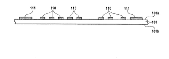
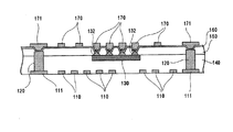
図1は本発明の好ましい実施の形態による半導体IC内蔵モジュール100の構造を示す略断面図である。
FIG. 1 is a schematic sectional view showing the structure of a semiconductor IC built-in
図1に示すように、本実施形態による半導体IC内蔵モジュール100は、積層された樹脂層140(第1の樹脂層)及び樹脂層150(第2の樹脂層)と、樹脂層140と樹脂層150との間に埋め込まれた半導体IC130と、樹脂層140の表面に埋め込まれるように設けられた下部基板配線パターン110,111(第1の基板配線パターン)と、樹脂層150の表面に設けられた上部基板配線パターン170,171(第2の基板配線パターン)と、上部基板配線パターン170,171の下部に設けられた下地導体層160と、樹脂層140及び樹脂層150内に埋め込まれるよう貫通して設けられ、下部基板配線パターン111と上部基板配線パターン171とを電気的に接続するポスト電極120と、樹脂層140の表面及び下部基板配線パターン110,111を覆う保護層180と、樹脂層150の表面及び上部基板配線パターン170,171を覆う保護層181とを備えて構成されている。半導体IC130の各ランド電極(図1には示されていない)上には、スタッドバンプ132がそれぞれ形成されており、各ランド電極は対応するスタッドバンプ132を介して、上部基板配線パターン170と電気的に接続されている。スタッドバンプ132は、図1に示すように、樹脂層150を貫通して設けられている。
As shown in FIG. 1, the semiconductor IC built-in
また、図1には示されていないが、保護層180,181の表面にはコンデンサ等の受動部品が搭載され、保護層180,181に設けられたビアホール(BVH)を介して下部基板配線パターン110,111又は上部基板配線パターン170,171に電気的に接続される。
Although not shown in FIG. 1, passive components such as capacitors are mounted on the surfaces of the
本実施形態による半導体IC内蔵モジュール100では、内蔵される半導体IC130は研磨により薄型化されており、これにより半導体IC内蔵モジュール100の全体の厚さを1mm以下、例えば、200μm程度まで薄くすることが可能である。また後述するように、本実施形態では、半導体IC130に設けられた各スタッドバンプ132の平面方向における位置がポスト電極120の平面方向における位置に対して実質的に固定的であり、このため、製造上、スタッドバンプ132と上部基板配線パターン170との相対的な位置関係にずれが生じることはほとんど無い。
In the semiconductor IC built-in
図2は、半導体IC130の構造を示す略斜視図である。
FIG. 2 is a schematic perspective view showing the structure of the
図2に示すように、半導体IC130はベアチップ状態の半導体ICであり、その表面130aには多数のランド電極131が備えられている。ランド電極131のピッチ(電極ピッチ)については特に限定されないが、本実施形態による半導体IC内蔵モジュール100では、ランド電極131と上部基板配線パターン170との相対的な位置関係にずれがほとんど生じないことから、電極ピッチが100μm以下、例えば60μmといった非常に狭い半導体ICを用いることが可能である。
As shown in FIG. 2, the
また、半導体IC130の裏面130bは研磨されており、これにより半導体IC130の厚さt(表面130aから裏面130bまでの距離)は、通常の半導体ICに比べて非常に薄くされている。半導体IC130の厚さtについては、特に限定されないが、200μm以下、例えば20〜50μm程度に設定することが好ましい。裏面130bの研磨は、ウエハの状態で多数の半導体ICに対して一括して行い、その後、ダイシングにより個別の半導体IC130に分離することが好ましい。研磨により薄くする前にダイシングによって個別の半導体IC130に分離した場合には、熱硬化性樹脂等により半導体IC130の表面130aを覆った状態で裏面130bを研磨すれば作業効率が良い。
In addition, the
また、各ランド電極131には、スタッドバンプ132が形成されている。スタッドバンプ132の大きさについては、電極ピッチに応じて適宜設定すればよく、例えば、電極ピッチが約100μmである場合には、径を30〜50μm程度、高さを40〜80μm程度に設定すればよい。スタッドバンプ132の形成は、ダイシングにより個別の半導体IC130に分離した後、ワイヤボンダーを用いて各ランド電極131にこれらを形成することにより行うことができる。スタッドバンプ132の材料としては、特に限定されるものではないが銅(Cu)を用いることが好ましい。スタッドバンプ132の材料として銅(Cu)を用いれば、金(Au)を用いた場合と比べ、ランド電極131に対して高い接合強度を得ることが可能となり、信頼性が高められる。
Each
次に、図1に示す半導体IC内蔵モジュール100の製造方法について、図面を参照しながら説明する。
Next, a method for manufacturing the semiconductor IC built-in
図3乃至図24は、図1に示す半導体IC内蔵モジュール100の製造方法を説明するための工程図である。
3 to 24 are process diagrams for explaining a method of manufacturing the semiconductor IC built-in
まず、転写用基板101(第1の転写用基板)を用意し、その表面101a及び裏面101bに感光性のドライフィルム102、103をそれぞれ貼り付ける(図3)。転写用基板101の材料としては、導電性を有する材料であればどのような材料を用いても構わないが、後の工程で剥離されることから、図1に示す樹脂層140との密着性が低い材料を用いることが好ましい。樹脂との密着性が低い材料としては、ニッケル(Ni)やステンレスを挙げることができる。転写用基板101の厚さについては、転写用基板として必要な機械的強度が確保される限り特に限定されず、例えば50μm程度に設定すればよい。一方、ドライフィルム102の厚さについては、下部基板配線パターン110,111よりもやや厚く設定する必要があり、例えば、下部基板配線パターン110,111の厚さを20μm程度とする場合には、ドライフィルム102の厚さとしては25μm程度に設定すればよい。ドライフィルム103は、後述するように、転写用基板101の裏面101bにメッキが施されるのを防止する目的で設けられるものであり、その厚さについては任意である。
First, a transfer substrate 101 (first transfer substrate) is prepared, and photosensitive
次に、フォトマスク(図示せず)を用いてドライフィルム102を露光し、下部基板配線パターン110、111を形成すべき領域110a、111aのドライフィルム102を除去する(図4)。これにより、領域110a及び領域111aにおいては、転写用基板101の表面101aが露出した状態となる。このときドライフィルム103の除去は行わず、これにより転写用基板101の裏面101bについては実質的に全面が覆われた状態を保っておく。
Next, the
このようにして転写用基板101の表面101aの一部を露出させた後、転写用基板101を基体とした電解メッキを行う。これにより、転写用基板101の表面101aが露出している領域110a、111aには、それぞれ下部基板配線パターン110、111が形成される(図5)。転写用基板101の裏面101bについては、実質的にその全面がドライフィルム103によって覆われていることから、メッキが形成されることはない。メッキ液の種類については、下部基板配線パターン110、111を構成すべき材料に応じて適宜選択すればよく、例えば、下部基板配線パターン110、111の材料を銅(Cu)とする場合には、メッキ液として硫酸銅を用いることができる。その後ドライフィルム102、103を剥離すれば、転写用基板101の表面101aに下部基板配線パターン110、111が形成された状態となる(図6)。
After exposing a part of the
次に、転写用基板101の表面101a及び裏面101bに別の感光性のドライフィルム104、105をそれぞれ貼り付ける(図7)。ドライフィルム104の厚さについては、ポスト電極120よりもやや厚く設定する必要があり、例えば、ポスト電極120の厚さを90μm程度とする場合には、ドライフィルム104の厚さとしては100μm程度に設定すればよい。一方、ドライフィルム105は、ドライフィルム103と同様、転写用基板101の裏面101bにメッキが施されるのを防止する目的で設けられるものであり、その厚さについては任意である。
Next, another photosensitive
次に、フォトマスク(図示せず)を用いてドライフィルム104を露光し、ポスト電極120を形成すべき領域120aのドライフィルム104を除去する(図8)。図8に示すように、ポスト電極120を形成すべき領域120aとは、下部基板配線パターン111の略中心部に対応する領域であり、これにより、領域120aにおいては下部基板配線パターン111が露出した状態となる。このときドライフィルム105の除去は行わず、これにより転写用基板101の裏面101bについては実質的に全面が覆われた状態を保っておく。
Next, the
このようにして下部基板配線パターン111の一部を露出させた後、転写用基板101を基体とした電解メッキを行う。これにより、下部基板配線パターン111が露出している領域120aには、ポスト電極120が形成される(図9)。転写用基板101の裏面101bについては、実質的にその全面がドライフィルム105によって覆われていることから、メッキが形成されることはない。メッキ液の選択については上述の通りであり、例えば硫酸銅を用いることができる。そして、ドライフィルム104、105を剥離すれば、転写用基板101の表面101aに下部基板配線パターン110、111及びポスト電極120が形成された状態となる(図10)。以上により、転写用基板101に対する加工が完了する。
After exposing a part of the lower
一方、転写用基板101とは別に転写用基板106(第2の転写用基板)を用意し、エッチングマスク(図示せず)を用いて所定の領域をエッチング除去することにより、複数の位置決め孔106a(第1の位置決め部)及び複数の位置決め孔106b(第2の位置決め部)を形成する(図11)。転写用基板106としては、転写用基板101と同じ材料及び同じ厚さのものを用いればよいが、転写用基板101とは異なり導電性を有している必要はない。但し、後の工程で剥離されることから、やはり樹脂層140との密着性が低い材料を用いることが好ましい。転写用基板106の材料として転写用基板101と同様の材料を用いた場合には、塩化第二鉄を用いたウエットエッチングにより位置決め孔106a,106bを形成することができる。
On the other hand, a transfer substrate 106 (second transfer substrate) is prepared separately from the
位置決め孔106aは、以下の工程でスタッドバンプ132を嵌合させることにより、半導体IC130を転写用基板106に位置決めした状態で仮止めするための孔である。したがって、その径としては、スタッドバンプ132の径とほぼ同じか、若干大き目に設定する必要がある。位置決め孔106aの径がスタッドバンプ132の径に比べて大きすぎると、半導体IC130を転写用基板106に仮止めできなくなるため、位置決め孔106aの径をあまり大きく設定すべきではない。また、半導体IC130を転写用基板106に位置決めした状態で仮止め可能である限り、全てのスタッドバンプ132に対応してこれと同数の位置決め孔106aを形成する必要はなく、図12に示すように、一部のスタッドバンプ132に対応する位置決め孔106aを設けるとともに、残りのスタッドバンプ132に対応する領域には、スタッドバンプ132の径よりも十分に大きな切り欠き106cを設けることによって、残りのスタッドバンプ132と転写用基板106との干渉を避けるよう構成しても構わない。
The
一方、位置決め孔106bは、以下の工程でポスト電極120を嵌合させることにより、転写用基板101に対して転写用基板106を位置決めするための孔である。したがって、その径としては、ポスト電極120の径よりも若干大き目に設定する必要がある。但し、位置決め孔106bの径がポスト電極120の径に比べて大きすぎると、位置決め精度が低下することから、位置決め孔106bの径をあまり大きく設定すべきではない。
On the other hand, the
このように、転写用基板106に形成する位置決め孔106a及び位置決め孔106bは、以下の工程でそれぞれスタッドバンプ132及びポスト電極120を嵌合させる孔であり、これらの相対的な位置関係についての精度を決める重要な要素であることから、精度良く形成することが求められる。したがって、加工精度が確保される限りにおいて他の方法、例えばドリルを用いてこれら位置決め孔106a,106bを形成しても構わない。以上により、転写用基板106に対する加工が完了する。
As described above, the
さらに、転写用基板101及び転写用基板106に対する加工とは別に、半導体IC130に対する加工を行う。半導体IC130に対する加工は、上述の通り、研磨による薄型化とスタッドバンプ132の形成の2つである。研磨による薄型化は、上述の通り、ウエハの状態で裏面130bを研磨し、その厚さtを200μm以下、例えば20〜50μm程度まで薄くした後、ダイシングにより個別の半導体IC130に分離することにより行うことができる。また、スタッドバンプ132の形成は、ダイシングにより個別の半導体IC130に分離した後、ワイヤボンダーを用いて各ランド電極131にこれらを形成することにより行うことができる。これにより、図2に示すように、薄型化され且つ各ランド電極131上にスタッドバンプ132が形成された半導体IC130を作製することができる。
Further, processing on the
このようにして転写用基板106に対する加工及び半導体IC130に対する加工が完了すると、転写用基板106に設けられた位置決め孔106aに半導体IC130のスタッドバンプ132を挿入し、これによって転写用基板106に半導体IC130を仮止めする(図13)。これにより、半導体IC130は転写用基板106に位置決めされた状態となる。
When the processing for the
次に、転写用基板106に設けられた位置決め孔106bにポスト電極120が挿入されるよう、転写用基板101に対して転写用基板106を位置決めしながら、転写用基板101と転写用基板106によってプリプレグ140aをプレスする(図14)。プリプレグ140aとは、炭素繊維、ガラス繊維、アラミド繊維等の繊維にエポキシ樹脂等の未硬化の熱硬化性樹脂を含浸させたシートであり、プレスしながら熱を加えることによってプリプレグ140aに含まれる熱硬化性樹脂を硬化させ、樹脂層140を形成する(図15)。これにより、下部基板配線パターン110、下部基板配線パターン111、ポスト電極120及び半導体IC130は、樹脂層140により一体化される。その後、転写用基板101及び転写用基板106を剥離し、一体化された積層体を取り出す(図16)。転写用基板101及び転写用基板106を剥離すると、図16に示すように、ポスト電極120及びスタッドバンプ132が突出した状態となる。ここで、ポスト電極120とスタッドバンプ132の平面的な位置関係は、転写用基板106に設けられた位置決め孔106aと位置決め孔106bの平面的な位置関係と実質的に一致しているため、両者の位置関係は実質的に固定的となる。
Next, the
次に、ポスト電極120及びスタッドバンプ132が突出している表面に、プリプレグ150aを被せ、突出しているポスト電極120及びスタッドバンプ132を完全に覆う(図17)。使用するプリプレグ150aとしては、樹脂層140の形成に用いたプリプレグ140aと同じ材料のものを用いればよい。そして、熱を加えることによりプリプレグ150aを硬化させて樹脂層150を形成した後、その表面を研磨又はブラストにより除去し、ポスト電極120及びスタッドバンプ132を露出させる(図18)。
Next, the surface from which the
次に、スパッタリング法等の気相成長法により、ポスト電極120及びスタッドバンプ132が露出している側の表面の全面に薄い下地導体層160を形成する(図19)。但し、下地導体層160の形成においては、気相成長法の代わりにメッキ法を用いても構わないし、金属箔の貼り付けによって下地導体層160を形成しても構わない。下地導体層160の不要部分はその後除去されることから、下地導体層160の厚さは十分に薄く設定する必要があり、例えば0.3μm程度に設定することが好ましい。
Next, a thin
次に、積層体の両面、つまり、樹脂層140の表面及び下地導体層160の表面に感光性のドライフィルム107、108をそれぞれ貼り付ける(図20)。ドライフィルム107の厚さについては、上部基板配線パターン170,171よりもやや厚く設定する必要があり、例えば、上部基板配線パターン170,171の厚さを20μm程度とする場合には、ドライフィルム107の厚さとしては25μm程度に設定すればよい。一方、ドライフィルム108は、下部基板配線パターン110,111が形成されている樹脂層140の表面にメッキが施されるのを防止する目的で設けられるものであり、その厚さについては任意である。
Next, photosensitive
次に、フォトマスク(図示せず)を用いてドライフィルム107を露光し、上部基板配線パターン170、171を形成すべき領域170a、171aのドライフィルム107を除去する(図21)。これにより、領域170a及び領域171aにおいては、下地導体層160が露出した状態となる。このときドライフィルム108の除去は行わず、これにより下部基板配線パターン110,111が形成されている樹脂層140の表面については実質的に全面が覆われた状態を保っておく。
Next, the
ここで、上部基板配線パターン170を形成すべき領域170aには、図21に示すように、スタッドバンプ132に対応する領域が含まれている。上述の通り、本実施形態においては、電極ピッチが非常に狭い半導体IC130が用いられることから、スタッドバンプ132と領域170aの平面方向における相対的な位置関係に大きなずれは許容されないが、スタッドバンプ132とポスト電極120の平面方向における相対的な位置関係は、上述の通り、実質的に固定されている。このことは、領域170aに対応するフォトマスクのパターンと、領域171aに対応するフォトマスクのパターンとの相対的な位置関係が、スタッドバンプ132とポスト電極120の平面方向における相対的な位置関係と実質的に一致することを意味するため、下地導体層160のうち、スタッドバンプ132に対応する領域を正確に露出させることが可能である。
Here, the
このようにして下地導体層160の一部を露出させた後、下地導体層160を基体とした電解メッキを行う。これにより、下地導体層160が露出している領域170a、171aには、それぞれ上部基板配線パターン170、171が形成される(図22)。樹脂層140の表面については、実質的にその全面がドライフィルム108によって覆われていることから、メッキが形成されることはない。メッキ液の選択については上述の通りであり、例えば硫酸銅を用いることができる。その後ドライフィルム107、108を剥離すれば、下地導体層160の表面に上部基板配線パターン170、171が形成された状態となる(図23)。
After exposing a part of the
そして、酸などのエッチング液を用いて上部基板配線パターン170、171が形成されていない部分の不要な下地導体層160を除去(ソフトエッチング)した後(図24)、積層体の両面を感光性の保護層180及び181で覆い、コンデンサ等の受動部品を搭載すべき領域に対応する部分の保護層180及び181を除去して下部基板配線パターン110及び上部基板配線パターン170の一部を露出させた後、受動部品を搭載することにより、図1に示した半導体IC内蔵モジュール100が完成する。
Then, an unnecessary
以上説明したように、本実施形態による半導体IC内蔵モジュール100の作製においては、位置決め孔106a,106b有する転写用基板106を用いていることから、スタッドバンプ132とポスト電極120の平面方向における相対的な位置関係が実質的に固定される。これにより、領域170aに対応するフォトマスクのパターンと、領域171aに対応するフォトマスクのパターンとの相対的な位置関係が、スタッドバンプ132とポスト電極120の平面方向における相対的な位置関係と実質的に一致することから、上部基板配線パターン170、171を形成する際、スタッドバンプ132に対して正確に位置合わせを行うことが可能となる。したがって、電極ピッチが100μm以下、例えば60μmといった非常に狭い半導体IC130を用いた場合であっても、ランド電極131及びスタッドバンプ132と上部基板配線パターン170との相対的な位置関係のずれを最小限に抑えることができる。
As described above, in the manufacture of the semiconductor IC built-in
しかも、本実施形態において用いている半導体IC130は、研磨によりその厚さtが非常に薄く設定されていることから、半導体IC内蔵モジュール100全体の厚さを非常に薄く、例えば200μm程度とすることが可能となる。
Moreover, since the thickness t of the
尚、上述した製造工程においては、樹脂層150を形成した後、その表面を研磨又はブラストにより除去することによってポスト電極120及びスタッドバンプ132を露出させているが(図18参照)、ポスト電極120及びスタッドバンプ132の露出をレーザ等を用いた孔開けにより行うことも可能である。以下、その方法について図面を参照しながら説明する。
In the manufacturing process described above, after the
図25乃至図31は、ポスト電極120及びスタッドバンプ132の露出を孔開けにより行う場合の製造方法を説明するための工程図である。
25 to 31 are process diagrams for explaining a manufacturing method in the case where the
まず、図17までの工程が完了した後、ポスト電極120及びスタッドバンプ132に対応する領域にレーザを照射することにより、樹脂層150に孔151を形成し、ポスト電極120及びスタッドバンプ132を露出させる(図25)。孔151の形成は、レーザの照射以外の方法を用いても構わない。
First, after the steps up to FIG. 17 are completed, a
その後の工程は、図19以降の工程と同様であり、ポスト電極120及びスタッドバンプ132が露出している側の表面の全面に薄い下地導体層160を形成した後(図26)、積層体の両面に感光性のドライフィルム107、108を貼り付け(図27)、図示しないフォトマスクを用いてドライフィルム107を露光することによって、領域170a、171aのドライフィルム107を除去する(図28)。次に、下地導体層160を基体とした電解メッキを行って、領域170a、171aにそれぞれ上部基板配線パターン170、171を形成する(図29)。そして、ドライフィルム107、108を剥離し(図30)、上部基板配線パターン170、171が形成されていない部分の不要な下地導体層160を除去(ソフトエッチング)する(図31)。その後は、積層体の両面を感光性の保護層180及び181で覆い、コンデンサ等の受動部品を搭載すべき領域に対応する部分の保護層180及び181を除去して下部基板配線パターン110及び上部基板配線パターン170の一部を露出させた後、受動部品を搭載することにより、半導体IC内蔵モジュールが完成する。
The subsequent process is the same as the process after FIG. 19, and after forming the thin
次に、本発明の好ましい他の実施の形態による半導体IC内蔵モジュールについて説明する。 Next, a semiconductor IC built-in module according to another preferred embodiment of the present invention will be described.
図32は本発明の好ましい他の実施の形態による半導体IC内蔵モジュール200の構造を示す略断面図である。
FIG. 32 is a schematic cross-sectional view showing the structure of a semiconductor IC built-in
図32に示すように、本実施形態による半導体IC内蔵モジュール200は、積層された樹脂層240及び樹脂層250と、樹脂層240と樹脂層250との間に埋め込まれた半導体IC230及び内部基板配線パターン290(第3の基板配線パターン)と、樹脂層240の表面に設けられた下部基板配線パターン210,211と、樹脂層250の表面に設けられた上部基板配線パターン270,271と、下部基板配線パターン210,211の樹脂層240側に設けられた下地導体層261と、上部基板配線パターン270,271の樹脂層250側に設けられた下地導体層260と、樹脂層240及び樹脂層250内に埋め込まれるよう貫通して設けられ、下部基板配線パターン211と上部基板配線パターン271とを電気的に接続するポスト電極220と、樹脂層240の表面及び下部基板配線パターン210,211を覆う保護層280と、樹脂層250の表面及び上部基板配線パターン270,271を覆う保護層281とを備えて構成されている。このように、本実施形態による半導体IC内蔵モジュール200は、上述した半導体IC内蔵モジュール100と比べると、内部基板配線パターン290が設けられている点、並びに、下部基板配線パターン210,211が樹脂層240に埋め込まれることなく、その表面上に設けられている点において主に異なっている。
As shown in FIG. 32, the semiconductor IC built-in
本実施形態による半導体IC内蔵モジュール200においても、保護層280,281の表面にコンデンサ等の受動部品が搭載され、保護層280,281に設けられたビアホール(BVH)を介して下部基板配線パターン210,211又は上部基板配線パターン270,271に電気的に接続される。また、内蔵される半導体IC230は、上述した半導体IC内蔵モジュール100において用いた半導体IC130と同様のものを用いることができ、図32に示すように、スタッドバンプ232を介して、上部基板配線パターン270と電気的に接続されている。
Also in the semiconductor IC built-in
次に、図32に示す半導体IC内蔵モジュール200の製造方法について、図面を参照しながら説明する。尚、本実施形態による半導体IC内蔵モジュール200の製造方法は、多くの部分において上述した半導体IC内蔵モジュール100の製造方法と類似していることから、重複する説明については一部省略することがある。
Next, a method for manufacturing the semiconductor IC built-in
図33乃至図49は、図32に示す半導体IC内蔵モジュール200の製造方法を説明するための工程図である。
33 to 49 are process diagrams for explaining a method of manufacturing the semiconductor IC built-in
まず、転写用基板201を用意し、エッチングマスク(図示せず)を用いて所定の領域をエッチング除去することにより、複数の位置決め孔201a及び複数の位置決め孔201bを形成する(図33)。転写用基板201としては、上述した転写用基板101と同じ材料及び同じ厚さのものを用いればよく、位置決め孔201a,201bの形成方法としては、転写用基板106に位置決め孔106a,106bを形成する方法と同様の方法を用いればよい。
First, a
位置決め孔201aは、以下の工程でスタッドバンプ232を嵌合させることにより、半導体IC230を転写用基板201に位置決めした状態で仮止めするための孔であり、したがって、その径としては、スタッドバンプ232の径とほぼ同じか、若干大き目に設定する必要がある。尚、図12を用いて説明したように、一部のスタッドバンプ232に対応する位置決め孔201aを設けるとともに、残りのスタッドバンプ232に対応する領域には、スタッドバンプ232の径よりも十分に大きな切り欠きを設けることによって、残りのスタッドバンプ232と転写用基板201との干渉を避けても構わない。一方、位置決め孔201bは、以下の工程でポスト電極220を嵌合させることにより、転写用基板201を後述する転写用基板206に対して位置決めするための孔である。
The
次に、転写用基板206の両面に感光性のドライフィルム202、203を貼り付け(図34)、フォトマスク(図示せず)を用いてドライフィルム203を露光することにより、内部基板配線パターン290を形成すべき領域290aのドライフィルム203を除去する(図35)。このとき、ドライフィルム202の除去は行わない。
Next, photosensitive
このようにして転写用基板201の裏面の一部を露出させた後、転写用基板201を基体とした電解メッキを行うことにより、領域290aに内部基板配線パターン290を形成する(図36)。その後ドライフィルム202、203を剥離すれば、転写用基板201の裏面に内部基板配線パターン290が形成された状態となる(図37)。
After exposing a part of the back surface of the
次に、上述した半導体IC130と同様の構造を有する半導体IC230を用意し、転写用基板201に設けられた位置決め孔201に半導体IC230のスタッドバンプ232を挿入することによって仮止めする(図38)。これにより、半導体IC230は、転写用基板201に位置決めされた状態となる。
Next, a
一方、転写用基板201とは別に転写用基板206を用意し、転写用基板201に内部基板配線パターン290を形成した方法と同様の方法を用いて、その表面に複数のポスト電極220を形成する。そして、転写用基板201に設けられた位置決め孔201bにポスト電極220が挿入されるよう、転写用基板201を転写用基板206に対して位置決めしながら、転写用基板201と転写用基板206によってプリプレグ240aをプレスする(図39)。この状態でプリプレグ240aに熱を加えて硬化させ、樹脂層240を形成する(図40)。これにより、内部基板配線パターン290、ポスト電極220及び半導体IC230は、樹脂層240により一体化される。その後、転写用基板201及び転写用基板206を剥離し、一体化された積層体を取り出す(図41)。ここで、ポスト電極220とスタッドバンプ232の平面的な位置関係は、転写用基板201に設けられた位置決め孔201aと位置決め孔201bの平面的な位置関係と実質的に一致しているため、両者の位置関係は実質的に固定的となる。
On the other hand, a
次に、ポスト電極220及びスタッドバンプ232が突出している表面に、プリプレグ250aを被せ、突出しているポスト電極220及びスタッドバンプ232を完全に覆う(図42)。そして、熱を加えることによりプリプレグ250aを硬化させて樹脂層250を形成した後、その表面を研磨又はブラストにより除去し、ポスト電極220及びスタッドバンプ232を露出させる(図43)。
Next, the surface from which the
次に、樹脂層250が形成されている側の表面の全面に薄い下地導体層260を形成するとともに、樹脂層240が形成されている側の表面の全面に薄い下地導体層261を形成する(図44)。つまり、積層体の両面に下地導体層を形成する。次に、積層体の両面、つまり、下地導体層260,261の表面に感光性のドライフィルム207、208をそれぞれ貼り付け(図45)、フォトマスク(図示せず)を用いてドライフィルム207,208を露光することにより、上部基板配線パターン270、271を形成すべき領域270a、271aのドライフィルム207、並びに、下部基板配線パターン210、211を形成すべき領域210a、211aのドライフィルム208を除去する(図46)。これにより、領域270a及び領域271aにおいては下地導体層260が露出した状態となり、領域210a及び領域211aにおいては下地導体層261が露出した状態となる。
Next, a thin
ここでも、上部基板配線パターン270を形成すべき領域270aには、図46に示すように、スタッドバンプ232に対応する領域が含まれているが、スタッドバンプ232とポスト電極220の平面方向における相対的な位置関係が実質的に固定されていることから、下地導体層260のうち、スタッドバンプ232に対応する領域を正確に露出させることが可能である。
Here, the
このようにして下地導体層260,261の一部を露出させた後、下地導体層260,261を基体とした電解メッキを行う。これにより、下地導体層260が露出している領域270a、271aにはそれぞれ上部基板配線パターン270、271が形成され、下地導体層261が露出している領域210a、211aにはそれぞれ下部基板配線パターン210、211が形成される(図47)。その後ドライフィルム207、208を剥離すれば、下地導体層260の表面に上部基板配線パターン270、271が形成され、下地導体層261の表面に下部基板配線パターン210、211が形成された状態となる(図48)。
Thus, after exposing a part of base conductor layers 260 and 261, electrolytic plating using base conductor layers 260 and 261 as a base is performed. As a result, upper
そして、エッチング液を用いて上部基板配線パターン270、271が形成されていない部分の不要な下地導体層260を除去(ソフトエッチング)するとともに、下部基板配線パターン210、211が形成されていない部分の不要な下地導体層261を除去(ソフトエッチング)した後(図49)、積層体の両面を感光性の保護層280及び281で覆い、コンデンサ等の受動部品を搭載すべき領域に対応する部分の保護層280及び281、さらには樹脂層250を除去して下部基板配線パターン210、上部基板配線パターン270及び内部配線パターン290の一部を露出させた後、受動部品を搭載することにより、図32に示した半導体IC内蔵モジュール200が完成する。
Then, an unnecessary
以上説明したように、本実施形態による半導体IC内蔵モジュール200の作製においては、位置決め孔201a,201b有する転写用基板201を用いていることから、スタッドバンプ232とポスト電極220の平面方向における相対的な位置関係が実質的に固定される。これにより、上記実施形態と同様、電極ピッチが100μm以下、例えば60μmといった非常に狭い半導体IC230を用いた場合であっても、スタッドバンプ232と上部基板配線パターン270との相対的な位置関係のずれを最小限に抑えることができる。
As described above, in the manufacture of the semiconductor IC built-in
さらに、本実施形態においては、内部基板配線パターン290が形成されることから、より複雑な配線パターンを施すことが可能となる。
Furthermore, in the present embodiment, since the internal
尚、上述した製造工程においては、樹脂層250を形成した後、その表面を研磨又はブラストにより除去することによってポスト電極220及びスタッドバンプ232を露出させているが(図43参照)、図25乃至図31を用いて説明したように、ポスト電極220及びスタッドバンプ232の露出をレーザ等を用いた孔開けにより行っても構わない。このとき、内部基板配線パターン290の一部についても孔開けにより露出させれば、内部基板配線パターン290と他の配線等との接続を容易に行うことが可能となる。
In the manufacturing process described above, after the
本発明は、以上説明した実施の形態に限定されることなく、特許請求の範囲に記載された発明の範囲内で種々の変更が可能であり、それらも本発明の範囲内に包含されるものであることはいうまでもない。 The present invention is not limited to the embodiments described above, and various modifications are possible within the scope of the invention described in the claims, and these are also included in the scope of the present invention. Needless to say.
例えば、図1に示した半導体IC内蔵モジュール100では、下部基板配線パターン110,111が樹脂層140に埋め込まれているが、図14に示すプレス工程において、転写用基板101の代わりに図39に示す転写用基板206を用い、その後、図44乃至図49に示す工程を実施することによって、樹脂層140の表面に下部基板配線パターン110,111を形成しても構わない。
For example, in the semiconductor IC built-in
逆に、図32に示した半導体IC内蔵モジュール200においても、図39に示すプレス工程において、転写用基板206の代わりに、図10及び図14に示す転写用基板101を用い、その後、図19乃至図24に示す工程を実施することによって、樹脂層240の内部に下部基板配線パターン210,211を埋め込んでも構わない。
On the contrary, in the semiconductor IC built-in
さらに、樹脂層140(240)の内部に埋め込まれた下部基板配線パターン110と、樹脂層140(240)の表面に形成された下部基板配線パターン210,211の両方を形成しても構わない。この場合、埋め込まれた下部基板配線パターン110と、表面に形成された下部基板配線パターン210,211との絶縁を図るため、樹脂層150(250)と同様の層をこれらの間に介在させる必要がある。
Further, both the lower
また、いずれの実施形態においても、最終的に転写用基板を剥離しているが、一方の転写用基板として例えば多数の内部配線が施された多層基板を用い、プレス後、これを剥離することなく半導体IC内蔵モジュールの一部としてそのまま使用することも可能である。例えば、図39に示すプレス工程において、ポスト電極220が形成された転写用基板206の代わりに、ポスト電極220が形成された多層基板を用い、これを剥離せず、そのまま基板として使用すればよい。
In any of the embodiments, the transfer substrate is finally peeled off. However, for example, a multi-layer substrate with a large number of internal wirings is used as one transfer substrate, and this is peeled off after pressing. Alternatively, it can be used as it is as a part of a module with a built-in semiconductor IC. For example, in the pressing step shown in FIG. 39, instead of the
さらに、いずれの実施形態においても、転写用基板106(201)に設けられた位置決め孔106b(201b)にポスト電極120(220)を挿入することにより、転写用基板101(206)に対して転写用基板106(201)を位置決めしているが(図14、図39参照)、位置決めの際にポスト電極を位置決め孔に挿入することは必須でない。例えば、ポスト電極の高さをプリプレグ(140a,240a)の厚さと同等程度に設定し、位置決め孔を介してポスト電極を画像認識することにより位置決めを行っても構わない。この場合、ポスト電極が位置決め孔に挿入されなくても、正しく位置決めを行うことが可能となる。また、ポスト電極を位置決め孔に挿入する場合であっても、画像認識による位置決めを併用すれば、位置決め孔の径をポスト電極の径に対して十分に大きく設定しても正しく位置決めすることが可能となり、作業効率を高めることが可能となる。
Further, in any of the embodiments, the post electrode 120 (220) is inserted into the
以上説明したように、本発明によれば、電極ピッチが非常に狭い半導体ICを用いた薄型の半導体IC内蔵モジュールを提供することが可能となる。 As described above, according to the present invention, it is possible to provide a thin semiconductor IC built-in module using a semiconductor IC having a very narrow electrode pitch.
100,200 半導体IC内蔵モジュール
101,106,201,206 転写用基板
101a 表面
101b 裏面
102〜105,107,108、202,203,207,208 ドライフィルム
106a,106b,201a,201b 位置決め孔
110,111,210,211 下部基板配線パターン
110a,111a,120a,170a,171a,210a,211a,270a,271a,290a ドライフィルムが除去された領域
120,220 ポスト電極
130,230 半導体IC
130a 表面
130b 裏面
131 ランド電極
132,232 スタッドバンプ
140,150,240,250 樹脂層
140a,150a,240a,250a プリプレグ
151 孔
160,260,261 下地導体層
170,171,270,271 上部基板配線パターン
180,181,280,281 保護層
290 内部基板配線パターン
100, 200 Semiconductor IC built-in
130a
Claims (5)
第2の転写用基板に第1及び第2の位置決め部を形成するステップと、
前記第1の位置決め部にバンプを位置決めしながら、前記第2の転写用基板に前記バンプを有する半導体ICを仮止めするステップと、
前記第2の位置決め部と前記ポスト電極によって前記第1の転写用基板を前記第2の転写用基板に対して位置決めしながら、前記第1及び第2の転写用基板によって樹脂をプレスし硬化させるステップとを備えることを特徴とする半導体IC内蔵モジュールの製造方法。 Forming a post electrode on the first transfer substrate;
Forming first and second positioning portions on a second transfer substrate;
Temporarily fixing the semiconductor IC having the bump on the second transfer substrate while positioning the bump on the first positioning portion;
While the first transfer substrate is positioned with respect to the second transfer substrate by the second positioning portion and the post electrode, the resin is pressed and cured by the first and second transfer substrates. A method of manufacturing a module with a built-in semiconductor IC.
Priority Applications (4)
| Application Number | Priority Date | Filing Date | Title |
|---|---|---|---|
| JP2004191369A JP3938921B2 (en) | 2003-07-30 | 2004-06-29 | Manufacturing method of semiconductor IC built-in module |
| US10/900,458 US7547975B2 (en) | 2003-07-30 | 2004-07-28 | Module with embedded semiconductor IC and method of fabricating the module |
| CNA2004100557098A CN1578601A (en) | 2003-07-30 | 2004-07-30 | Module with embedded semiconductor and method of fabricating the module |
| EP04254569.9A EP1503409B1 (en) | 2003-07-30 | 2004-07-30 | Module with embedded semiconductor IC which has a narrow electrode pitch and method of fabricating the module |
Applications Claiming Priority (2)
| Application Number | Priority Date | Filing Date | Title |
|---|---|---|---|
| JP2003283243 | 2003-07-30 | ||
| JP2004191369A JP3938921B2 (en) | 2003-07-30 | 2004-06-29 | Manufacturing method of semiconductor IC built-in module |
Publications (3)
| Publication Number | Publication Date |
|---|---|
| JP2005064470A JP2005064470A (en) | 2005-03-10 |
| JP2005064470A5 JP2005064470A5 (en) | 2005-09-02 |
| JP3938921B2 true JP3938921B2 (en) | 2007-06-27 |
Family
ID=34380217
Family Applications (1)
| Application Number | Title | Priority Date | Filing Date |
|---|---|---|---|
| JP2004191369A Active JP3938921B2 (en) | 2003-07-30 | 2004-06-29 | Manufacturing method of semiconductor IC built-in module |
Country Status (1)
| Country | Link |
|---|---|
| JP (1) | JP3938921B2 (en) |
Families Citing this family (24)
| Publication number | Priority date | Publication date | Assignee | Title |
|---|---|---|---|---|
| US7547975B2 (en) | 2003-07-30 | 2009-06-16 | Tdk Corporation | Module with embedded semiconductor IC and method of fabricating the module |
| TW200618705A (en) | 2004-09-16 | 2006-06-01 | Tdk Corp | Multilayer substrate and manufacturing method thereof |
| JP2006339354A (en) | 2005-06-01 | 2006-12-14 | Tdk Corp | Semiconductor ic and its manufacturing method, module with built-in semiconductor ic and its manufacturing method |
| JP4535002B2 (en) | 2005-09-28 | 2010-09-01 | Tdk株式会社 | Semiconductor IC-embedded substrate and manufacturing method thereof |
| US8188375B2 (en) | 2005-11-29 | 2012-05-29 | Tok Corporation | Multilayer circuit board and method for manufacturing the same |
| JP4835124B2 (en) * | 2005-11-29 | 2011-12-14 | Tdk株式会社 | Semiconductor IC-embedded substrate and manufacturing method thereof |
| JP2007194436A (en) * | 2006-01-19 | 2007-08-02 | Elpida Memory Inc | Semiconductor package and manufacturing method thereof, substrate with conductive post, and laminated semiconductor device and manufacturing method thereof |
| US20100044845A1 (en) * | 2006-04-27 | 2010-02-25 | Nec Corporation | Circuit substrate, an electronic device arrangement and a manufacturing process for the circuit substrate |
| JP4274290B2 (en) * | 2006-11-28 | 2009-06-03 | 国立大学法人九州工業大学 | Manufacturing method of semiconductor device having double-sided electrode structure |
| JP4303282B2 (en) | 2006-12-22 | 2009-07-29 | Tdk株式会社 | Wiring structure of printed wiring board and method for forming the same |
| JP4331769B2 (en) | 2007-02-28 | 2009-09-16 | Tdk株式会社 | Wiring structure, method for forming the same, and printed wiring board |
| JP5193503B2 (en) * | 2007-06-04 | 2013-05-08 | 新光電気工業株式会社 | Substrate with through electrode and method for manufacturing the same |
| JP5654109B2 (en) * | 2007-09-18 | 2015-01-14 | オリンパス株式会社 | Manufacturing method of laminated mounting structure |
| JP5690466B2 (en) * | 2008-01-31 | 2015-03-25 | インヴェンサス・コーポレイション | Manufacturing method of semiconductor chip package |
| JP2009246104A (en) * | 2008-03-31 | 2009-10-22 | Kyushu Institute Of Technology | Electronic component for wiring and its manufacturing method |
| JP5268459B2 (en) * | 2008-07-10 | 2013-08-21 | 株式会社半導体エネルギー研究所 | Semiconductor device |
| JPWO2010024233A1 (en) * | 2008-08-27 | 2012-01-26 | 日本電気株式会社 | Wiring board capable of incorporating functional elements and method for manufacturing the same |
| JP5436837B2 (en) * | 2008-10-30 | 2014-03-05 | 新光電気工業株式会社 | Manufacturing method of semiconductor device embedded substrate |
| JP5491722B2 (en) * | 2008-11-14 | 2014-05-14 | インヴェンサス・コーポレイション | Semiconductor device package structure and manufacturing method thereof |
| JP2010205851A (en) * | 2009-03-02 | 2010-09-16 | Shinko Electric Ind Co Ltd | Semiconductor device and method of manufacturing the same, and electronic device |
| JPWO2011024939A1 (en) * | 2009-08-28 | 2013-01-31 | 日本電気株式会社 | Semiconductor device and manufacturing method thereof |
| JP6320681B2 (en) * | 2013-03-29 | 2018-05-09 | ローム株式会社 | Semiconductor device |
| KR102144367B1 (en) * | 2013-10-22 | 2020-08-14 | 삼성전자주식회사 | Semiconductor package and method of fabricating the same |
| JP6317629B2 (en) * | 2014-06-02 | 2018-04-25 | 株式会社東芝 | Semiconductor device |
-
2004
- 2004-06-29 JP JP2004191369A patent/JP3938921B2/en active Active
Also Published As
| Publication number | Publication date |
|---|---|
| JP2005064470A (en) | 2005-03-10 |
Similar Documents
| Publication | Publication Date | Title |
|---|---|---|
| JP3938921B2 (en) | Manufacturing method of semiconductor IC built-in module | |
| US7547975B2 (en) | Module with embedded semiconductor IC and method of fabricating the module | |
| JP3069010B2 (en) | Multi-chip module with interconnect decals manufactured on mandrel | |
| KR101344800B1 (en) | Wiring board and semiconductor device | |
| JP4535002B2 (en) | Semiconductor IC-embedded substrate and manufacturing method thereof | |
| US9589920B2 (en) | Chip package | |
| JP5101451B2 (en) | Wiring board and manufacturing method thereof | |
| JP5263918B2 (en) | Semiconductor device and manufacturing method thereof | |
| JP2008300507A (en) | Wiring substrate and manufacturing process of the same | |
| JP2004193549A (en) | Package substrate plated without plated lead-in wire and its manufacturing method | |
| TWI505756B (en) | Printed circuit board and method for manufacturing the same | |
| US9334576B2 (en) | Wiring substrate and method of manufacturing wiring substrate | |
| CN109788666B (en) | Circuit substrate and manufacturing method thereof | |
| JP2005223223A (en) | Semiconductor ic built-in substrate, its manufacturing method, and semiconductor ic built-in module | |
| US6340840B1 (en) | Lead frame and production method thereof, and semiconductor device and fabrication method thereof | |
| JP2005353837A (en) | Semiconductor device and its manufacturing method | |
| US7963031B2 (en) | Package for semiconductor device and method of manufacturing the same | |
| JP2005236039A (en) | Substrate comprising built-in semiconductor ic and manufacturing method thereof, and module comprising built-in semiconductor ic | |
| JP2006049822A (en) | Module with built-in semiconductor ic | |
| JP2003188205A (en) | Semiconductor device, laminated semiconductor device and manufacturing method of the semiconductor device | |
| JP2002076166A (en) | Resin sealing type semiconductor device and its manufacturing method | |
| US20230275015A1 (en) | Interconnect substrate and method of making the same | |
| JP2005235982A (en) | Wiring substrate and its manufacturing method, and semiconductor package | |
| KR101617023B1 (en) | Method of manufacturing PCB substrate having metal post | |
| JP2023061259A (en) | Wiring board and method of manufacturing the same |
Legal Events
| Date | Code | Title | Description |
|---|---|---|---|
| A521 | Written amendment |
Free format text: JAPANESE INTERMEDIATE CODE: A523 Effective date: 20050512 |
|
| A621 | Written request for application examination |
Free format text: JAPANESE INTERMEDIATE CODE: A621 Effective date: 20050512 |
|
| A977 | Report on retrieval |
Free format text: JAPANESE INTERMEDIATE CODE: A971007 Effective date: 20070207 |
|
| A131 | Notification of reasons for refusal |
Free format text: JAPANESE INTERMEDIATE CODE: A131 Effective date: 20070213 |
|
| A521 | Written amendment |
Free format text: JAPANESE INTERMEDIATE CODE: A523 Effective date: 20070301 |
|
| TRDD | Decision of grant or rejection written | ||
| A01 | Written decision to grant a patent or to grant a registration (utility model) |
Free format text: JAPANESE INTERMEDIATE CODE: A01 Effective date: 20070323 |
|
| A61 | First payment of annual fees (during grant procedure) |
Free format text: JAPANESE INTERMEDIATE CODE: A61 Effective date: 20070326 |
|
| R150 | Certificate of patent or registration of utility model |
Ref document number: 3938921 Country of ref document: JP Free format text: JAPANESE INTERMEDIATE CODE: R150 Free format text: JAPANESE INTERMEDIATE CODE: R150 |
|
| FPAY | Renewal fee payment (event date is renewal date of database) |
Free format text: PAYMENT UNTIL: 20110406 Year of fee payment: 4 |
|
| FPAY | Renewal fee payment (event date is renewal date of database) |
Free format text: PAYMENT UNTIL: 20110406 Year of fee payment: 4 |
|
| FPAY | Renewal fee payment (event date is renewal date of database) |
Free format text: PAYMENT UNTIL: 20120406 Year of fee payment: 5 |
|
| FPAY | Renewal fee payment (event date is renewal date of database) |
Free format text: PAYMENT UNTIL: 20130406 Year of fee payment: 6 |
|
| FPAY | Renewal fee payment (event date is renewal date of database) |
Free format text: PAYMENT UNTIL: 20140406 Year of fee payment: 7 |