EP1729197A1 - A low-drop out (LDO) voltage regulator with pole zero compensation. - Google Patents
A low-drop out (LDO) voltage regulator with pole zero compensation. Download PDFInfo
- Publication number
- EP1729197A1 EP1729197A1 EP06114730A EP06114730A EP1729197A1 EP 1729197 A1 EP1729197 A1 EP 1729197A1 EP 06114730 A EP06114730 A EP 06114730A EP 06114730 A EP06114730 A EP 06114730A EP 1729197 A1 EP1729197 A1 EP 1729197A1
- Authority
- EP
- European Patent Office
- Prior art keywords
- terminal
- current control
- input terminal
- output
- amplifier
- Prior art date
- Legal status (The legal status is an assumption and is not a legal conclusion. Google has not performed a legal analysis and makes no representation as to the accuracy of the status listed.)
- Withdrawn
Links
Images

Classifications
-
- H—ELECTRICITY
- H03—ELECTRONIC CIRCUITRY
- H03F—AMPLIFIERS
- H03F1/00—Details of amplifiers with only discharge tubes, only semiconductor devices or only unspecified devices as amplifying elements
- H03F1/34—Negative-feedback-circuit arrangements with or without positive feedback
-
- G—PHYSICS
- G05—CONTROLLING; REGULATING
- G05F—SYSTEMS FOR REGULATING ELECTRIC OR MAGNETIC VARIABLES
- G05F1/00—Automatic systems in which deviations of an electric quantity from one or more predetermined values are detected at the output of the system and fed back to a device within the system to restore the detected quantity to its predetermined value or values, i.e. retroactive systems
- G05F1/10—Regulating voltage or current
- G05F1/46—Regulating voltage or current wherein the variable actually regulated by the final control device is dc
- G05F1/56—Regulating voltage or current wherein the variable actually regulated by the final control device is dc using semiconductor devices in series with the load as final control devices
- G05F1/575—Regulating voltage or current wherein the variable actually regulated by the final control device is dc using semiconductor devices in series with the load as final control devices characterised by the feedback circuit
Definitions
- the present invention relates to the field of electronics, and in particular to negative feedback amplifier systems, such as low-dropout voltage regulators.
- LDO Low dropout voltage
- dc direct current
- LDO regulators are characterized by low dropout voltages (i.e., a minimal difference between an unregulated input voltage, such as a voltage received from a battery or transformer, and the regulated (stable) output voltage).
- An LDO regulator fails to maintain its regulated voltage level (i.e., drops out of regulation) when the unregulated input voltage falls below the regulated output voltage plus the dropout voltage.
- the low dropout voltage of the LDO regulator effectively extends the life of the battery by providing a regulated voltage even if the battery is discharged to a value that is within (typically) 100-500 millivolts of the regulated voltage.
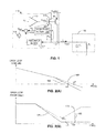
- Fig. 4 shows a conventional LDO regulator 10 that is connected to a load 50.
- LDO 10 includes an operational-amplifier (op-amp) 11, a PMOS transistor M, feedback resistors R11 and R12, and a reference voltage supply REF.
- Load 50 is represented by a resistive load R L and a capacitive load C L .
- a voltage supply (not shown) applies an input voltage V IN to one terminal of PMOS transistor M, and a portion of the output signal V OUT supplied to load 50 through PMOS transistor M is fed back by way of the feedback resistor R11 and R12 to the non-inverting input terminal of op-amp 11, which receives a stable reference signal from reference voltage supply REF on its inverting input terminal.
- op-amp 11 In response to the feedback signal and the reference signal, op-amp 11 generates an output signal that controls PMOS transistor M to regulate the output signal V OUT .
- a very serious problem associated with conventional LDO regulator 10 is that it is not stable for all capacitive loads C L .
- Known solutions can stabilize this circuit for values of C L larger than approximately 1 uF.
- Another restriction associated with this circuit is that capacitive load C L must have a low and very well-defined equivalent series resistance.
- a conventional voltage control loop of an LDO regulator has two dominant poles.
- the first pole is created at the output by the load equivalent resistor and the load capacitor.
- the second pole is located in the control error amplifier (e.g., op-amp 11). Due to the large loop gain of the system, the closed loop response will become quite under-damped.
- a way to improve and stabilize the control loop is by adding a zero in the loop gain.
- One traditional effective method to create such a zero is to insert a resistor in series with the load capacitor. This approach has the drawback that higher frequency disturbances (for instance due to load variations or ripple on the power line) are not effectively reduced.
- the parasitic series impedance of the load capacitor is usually not very well controlled, unless expensive capacitors are used. Sometimes the zero is created in the control error amplifier, but this usually requires large resistor values, which is counterproductive on silicon real estate.
- the present invention is directed to an improved negative feedback amplifier system (e.g., a control circuit) that utilizes a new method of creating a zero in the open loop gain in which part of the supplied output current is diverted through a "zero" resistor before adding it to the output voltage.
- the voltage signal developed at this "zero" resistor in response to the partial output current mimics the magnitude and phase of a zero in the open loop transfer function, and can be fed back to any suitable node in the control loop to increase the phase margin, thus improving the stability and step response of the amplifier system.
- this voltage signal can be added to the loop gain using a bypass capacitor that is coupled to an input terminal of the error amplifier. In this way, the voltage signal improves the phase margin over conventional feedback loops that exhibit marginal stability due to unavoidable parasitic elements which add non-dominant poles or right hand plane zeros.
- a portable device in accordance with a specific embodiment of the present invention, includes a battery (or other power source), a load circuit, and an LDO regulator connected between the battery and the load circuit.
- the LDO regulator includes a first current control element, an output stabilization circuit, and an error amplifier.
- the first current control element passes a portion of the unregulated battery voltage to the load circuit in response to a control signal generated by the error amplifier.
- the output stabilization circuit includes a second current control element and the "zero" resistor that are connected in series between the battery and the load circuit (i.e., parallel with the first current control element).
- the second current control element is also controlled by the control signal generated by the error amplifier, but is smaller than the first current control element.
- the output signal applied to the load circuit includes both the larger portion passed by the first switching circuit and a smaller component passed by the "zero" resistor.
- a zero signal generated at a node located between the second current control element and the "zero" resistor is added to the feedback signal, e.g., by way of a bypass capacitor, and the resulting feedback signal is compared by the error amplifier with a fixed reference voltage to generate the control signal.
- the output voltage can be divided down in a traditional manner to set the output voltage level.
- it can be inserted at another suitable point inside the error amplifier to realize the desired effect of the zero in the loop gain.
- Fig. is a simplified schematic diagram showing a negative feedback amplifier system according to a generalized embodiment of the present invention.
- Figs. 2(A) and 2(B) are Bode diagrams depicting operating characteristics associated with the negative feedback amplifier system of Fig. 1;
- Fig. 3 is a simplified schematic diagram showing a portable device including an LDO regulator according to a specific embodiment of the present invention.
- Fig. 4 is a simplified schematic diagram showing a conventional LDO regulator.
- Coupled refers to an electrical path between two elements that may include zero or more active or passive elements
- connected refers to a direct connection between two elements by way of a relatively conductive (e.g., metal) wire or trace.
- Fig. 1 shows a negative feedback amplifier system 110 according to a generalized embodiment of the present invention.
- Amplifier system 110 is connected between a voltage supply V SUPPLY (not shown) and a capacitive load circuit 150, which for simplicity is represented by a load resistor R L and a load capacitor C L .
- amplifier system 110 receives a reference signal V REF from a reference voltage source 114, which in one embodiment includes a circuit integrally formed with amplifier system 110, and in another embodiment represents an external signal source.
- V REF reference signal
- the operation of such negative feedback amplifier systems is well known to those skilled in the art.
- Amplifier system 110 includes a loop amplifier 113, an output device (first current control element) M1, an output stabilization circuit 115, a summing circuit 116, and a feedback block 117.
- loop amplifier 113 is controlled by a feedback signal V S , which at least in part is generated by output voltage V OUT , and generates a control signal V CNTL in response to feedback signal V S that is used to control output device M1 and output stabilization circuit 115 to maintain output voltage V OUT at a desired level.
- Output device M1 has a first terminal connected to supply voltage V SUPPLY , a control terminal, and a second terminal connected to an output terminal 112.
- Output device M1 includes any suitable active device (e.g., a P-type MOSFET, an N-type MOSFET, a PNP bipolar transistor, or an NPN bipolar transistor), and is sized to provide the majority of output load current I L .
- Output stabilization circuit 115 includes a second output device (second current control element) M2 that is connected in series with a "zero generating" (first) resistor R Z between supply voltage V SUPPLY and output terminal 112.
- Output device M2 is equivalent to output device M1 (i.e., same type (e.g., NMOS or PMOS) to assure matching and to define the current ratio current properly), but is sized to supply a small, but fixed, part of I L .
- a signal voltage is created at a node X (between output device M2 and resistor R Z ) which mimics the phase and magnitude as if a zero was inserted in the loop gain.
- the phase margin of the loop can be increased, resulting in better stability, frequency and step response.
- An example of such a convenient point is depicted in Fig. 1 as being an input to summing circuit 116.
- a high pass filter 118 can be implemented, for instance, in the form of a bypass capacitor.
- Feedback block 117 comprises, for example, a resistive voltage divider that serves to apply a predetermined portion of V OUT to summing circuit 116, which is combined with the signal from node X and the reference voltage from reference voltage source 114.
- Figs. 2(A) and 2(B) are Bode diagrams showing the effect of the present invention on open loop gain and phase characteristics compared to conventional negative feedback amplifier circuits.
- the negative feedback amplifier circuit of the present invention operates essentially the same as conventional negative feedback amplifier circuits.
- the open loop gain 165 of the negative feedback amplifier circuit of the present invention decreases less rapidly, thus crossing the 0 dB gain point at a frequency ⁇ 2 that is substantially higher than the 0 dB gain point ⁇ 1 associated with the open loop gain 160 of conventional negative feedback amplifier circuits.
- the effect of this increased gain at high frequencies on phase margin is indicated in Fig.
- the present invention provides an improved phase margin that improves stability. This means that after a sudden change in the applied load, the regulated output voltage V OUT will return faster to its nominal value and without excessive ringing.
- Fig. 3 is a simplified schematic diagram showing a portable device 200 including an LDO regulator (negative feedback amplifier circuit) 210 according to a specific embodiment of the present invention.
- Portable device 200 is, for example, one of a cellular phone, a cordless phone, a pager, a personal digital assistant, a portable personal computer, a camcorder, and a digital camera, that includes a battery (power source) 205 and a load integrated circuit (IC) 250, which for simplicity is represented by a load resistor R L and a load capacitor C L .
- LDO regulator 210 receives an unregulated input voltage V IN from battery 205 at its input terminal 211, and generates a regulated output signal V OUT at its output terminal 212 that is provided to load IC 250, thus facilitating the operation of portable device 200.
- LDO regulator 210 includes a (first) current control element M1 that is preferably connected (but may be coupled) between input terminal 211 and output terminal 212, an error amplifier 213 for generating a control signal V CNTL that is applied to the control terminal of current control element M1, and an output stabilization circuit 215.
- Current control element M1 is in one embodiment a PMOS or NMOS transistor, and in another embodiment a PNP or NPN bipolar transistor.
- Error amplifier 213 is an operational amplifier having an inverting input terminal coupled to a reference voltage source 214 and a non-inverting terminal coupled to a node Y, and provides a stable reference voltage V REF according to known techniques.
- Output stabilization circuit 215 is connected in parallel with current control element M1 between input terminal 211 and output terminal 212, and provides a stabilization signal to node Y by way of a bypass capacitor (high pass filter) 218 having a capacitance C BP .
- Feedback block 217 includes a voltage divider formed by resistors R 11 and R 12 , and feeds back a portion of output voltage V OUT to node Y, where this portion is combined with the stabilization signal to produce a feedback voltage V FB that is applied to the non-inverting terminal of error amplifier 213.
- output stabilization circuit 215 includes a (second) current control element M2, a "zero generating" (first) resistor R Z , and bypass capacitor 218.
- Current control element M2 has a first terminal preferably connected (but may be coupled) to input terminal 211, a control terminal connected to the output terminal of error amplifier 213, and a second terminal connected to a node N.
- Resistor R Z (which may be implemented by one or more separate resistance elements) is connected between node N and output terminal 212.
- Bypass capacitor 218 has a first terminal connected to node N, and a second terminal connected to node Y.
- output stabilization circuit 215 diverts part of the supplied load current I L through resistor R Z before adding it to the output load formed by load resistor R L and load capacitor C L .
- the voltage developed across resistor R L mimics the magnitude and phase of a zero in the Laplace transform of the transfer function of the open loop gain (i.e., a zero in the rational Laplace transform function representing the combined circuit formed by output stabilization circuit 215 and load IC 250).
- This mimicking signal is then passed through bypass capacitor, which provides a DC-block so that the DC value of the output voltage does not get imposed upon the signal Y, but only passes it's AC component.
- the partition of the total load current is conventionally determined by the ratio of the sizes (i.e., channel widths) of current control elements (e.g., PMOS transistors) M1 and M2. If n is defined as the ratio of these sizes as n equals M2/M1 (usually n ⁇ 1), then the value of the zero signal V Z has a time constant approximately equal to C L *nR Z *RL/(nR Z +R L ), which is in most practical cases close to C L *nR Z .
- the benefits of using output stabilization circuit 215 in this manner are to provide a stable output signal V OUT over a large load range, to avoid degradation of the ripple rejection at higher frequencies (which is a problem with conventional approaches).
- output stabilization circuit 215 is better controlled than in conventional approaches because it is less dependent on the uncontrollable parasitic resistor of the load capacitance C L .
- output stabilization circuit 215 can be fully integrated (i.e., fabricated on the same substrate as load IC 250 using the same process flow).
- portable device 200 is a cell phone using a battery that generates an unregulated input voltage V IN of approximately 4V (fully charged), and has an effective load resistor R L value of 30 ⁇ and an effective load capacitance C L of 1 ⁇ F.
- current control elements M1 and M2 are PMOS transistors having sizes 50000/0.5 ⁇ m and 100/0.5 ⁇ m, respectively, zero resistor R Z has a resistance value of 80 ⁇ , bypass capacitor C BP has a capacitance value of 30pF, V REF is maintained at 1.25V using known techniques.
- the output stabilization circuit 215 may be used in any negative feedback control circuit having a significant capacitive load (i.e., the capacitive output load forms a dominant pole in the loop gain).
Abstract
Description
- The present invention relates to the field of electronics, and in particular to negative feedback amplifier systems, such as low-dropout voltage regulators.
- Low dropout voltage (LDO) regulators are utilized to generate stable direct current (dc) voltages, for example, in portable, battery-operated devices such as cellular phones, cordless phones, pagers, personal digital assistants, portable personal computers, camcorders, and digital cameras. The demand for low dropout voltage (LDO) regulators has increased in direct proportion to the increased demand for such portable devices.
- LDO regulators are characterized by low dropout voltages (i.e., a minimal difference between an unregulated input voltage, such as a voltage received from a battery or transformer, and the regulated (stable) output voltage). An LDO regulator fails to maintain its regulated voltage level (i.e., drops out of regulation) when the unregulated input voltage falls below the regulated output voltage plus the dropout voltage. Thus, by minimizing the dropout voltage, an LDO regulator allows a portable device to operate longer from a single battery charge. That is, the low dropout voltage of the LDO regulator effectively extends the life of the battery by providing a regulated voltage even if the battery is discharged to a value that is within (typically) 100-500 millivolts of the regulated voltage.
- Fig. 4 shows a
conventional LDO regulator 10 that is connected to aload 50. LDO 10 includes an operational-amplifier (op-amp) 11, a PMOS transistor M, feedback resistors R11 and R12, and a reference voltage supply REF.Load 50 is represented by a resistive load RL and a capacitive load CL. In operation, a voltage supply (not shown) applies an input voltage VIN to one terminal of PMOS transistor M, and a portion of the output signal VOUT supplied to load 50 through PMOS transistor M is fed back by way of the feedback resistor R11 and R12 to the non-inverting input terminal of op-amp 11, which receives a stable reference signal from reference voltage supply REF on its inverting input terminal. In response to the feedback signal and the reference signal, op-amp 11 generates an output signal that controls PMOS transistor M to regulate the output signal VOUT. - A very serious problem associated with
conventional LDO regulator 10 is that it is not stable for all capacitive loads CL. Known solutions can stabilize this circuit for values of CL larger than approximately 1 uF. Another restriction associated with this circuit is that capacitive load CL must have a low and very well-defined equivalent series resistance. - A conventional voltage control loop of an LDO regulator has two dominant poles. The first pole is created at the output by the load equivalent resistor and the load capacitor. The second pole is located in the control error amplifier (e.g., op-amp 11). Due to the large loop gain of the system, the closed loop response will become quite under-damped. A way to improve and stabilize the control loop is by adding a zero in the loop gain. One traditional effective method to create such a zero, is to insert a resistor in series with the load capacitor. This approach has the drawback that higher frequency disturbances (for instance due to load variations or ripple on the power line) are not effectively reduced. Also, the parasitic series impedance of the load capacitor is usually not very well controlled, unless expensive capacitors are used. Sometimes the zero is created in the control error amplifier, but this usually requires large resistor values, which is counterproductive on silicon real estate.
- What is needed is an improved negative feedback amplifier system, such as a low-dropout voltage regulator, that is stable over a large load range, does not degrade the ripple rejection at higher frequencies, and minimizes stability dependence on the parasitic resistor of the output capacitor.
- The present invention is directed to an improved negative feedback amplifier system (e.g., a control circuit) that utilizes a new method of creating a zero in the open loop gain in which part of the supplied output current is diverted through a "zero" resistor before adding it to the output voltage. The voltage signal developed at this "zero" resistor in response to the partial output current mimics the magnitude and phase of a zero in the open loop transfer function, and can be fed back to any suitable node in the control loop to increase the phase margin, thus improving the stability and step response of the amplifier system. For example, this voltage signal can be added to the loop gain using a bypass capacitor that is coupled to an input terminal of the error amplifier. In this way, the voltage signal improves the phase margin over conventional feedback loops that exhibit marginal stability due to unavoidable parasitic elements which add non-dominant poles or right hand plane zeros.
- In accordance with a specific embodiment of the present invention, a portable device includes a battery (or other power source), a load circuit, and an LDO regulator connected between the battery and the load circuit. The LDO regulator includes a first current control element, an output stabilization circuit, and an error amplifier. The first current control element passes a portion of the unregulated battery voltage to the load circuit in response to a control signal generated by the error amplifier. The output stabilization circuit includes a second current control element and the "zero" resistor that are connected in series between the battery and the load circuit (i.e., parallel with the first current control element). The second current control element is also controlled by the control signal generated by the error amplifier, but is smaller than the first current control element. Thus, the output signal applied to the load circuit includes both the larger portion passed by the first switching circuit and a smaller component passed by the "zero" resistor. A zero signal generated at a node located between the second current control element and the "zero" resistor is added to the feedback signal, e.g., by way of a bypass capacitor, and the resulting feedback signal is compared by the error amplifier with a fixed reference voltage to generate the control signal. Before addition of the two feedback signals, the output voltage can be divided down in a traditional manner to set the output voltage level. As an alternative to adding the zero signal to the divided down feedback signal, it can be inserted at another suitable point inside the error amplifier to realize the desired effect of the zero in the loop gain.
- These and other features, aspects and advantages of the present invention will become better understood with regard to the following description, appended claims, and accompanying drawings, where:
- Fig. is a simplified schematic diagram showing a negative feedback amplifier system according to a generalized embodiment of the present invention;
- Figs. 2(A) and 2(B) are Bode diagrams depicting operating characteristics associated with the negative feedback amplifier system of Fig. 1;
- Fig. 3 is a simplified schematic diagram showing a portable device including an LDO regulator according to a specific embodiment of the present invention; and
- Fig. 4 is a simplified schematic diagram showing a conventional LDO regulator.
- As used herein, the term "coupled" refers to an electrical path between two elements that may include zero or more active or passive elements, and the term "connected" refers to a direct connection between two elements by way of a relatively conductive (e.g., metal) wire or trace.
- Fig. 1 shows a negative
feedback amplifier system 110 according to a generalized embodiment of the present invention.Amplifier system 110 is connected between a voltage supply VSUPPLY (not shown) and acapacitive load circuit 150, which for simplicity is represented by a load resistor RL and a load capacitor CL. In addition,amplifier system 110 receives a reference signal VREF from a reference voltage source 114, which in one embodiment includes a circuit integrally formed withamplifier system 110, and in another embodiment represents an external signal source. The operation of such negative feedback amplifier systems is well known to those skilled in the art. -
Amplifier system 110 includes aloop amplifier 113, an output device (first current control element) M1, anoutput stabilization circuit 115, asumming circuit 116, and afeedback block 117. Characteristic of all negative feedback control circuits,loop amplifier 113 is controlled by a feedback signal VS, which at least in part is generated by output voltage VOUT, and generates a control signal VCNTL in response to feedback signal VS that is used to control output device M1 andoutput stabilization circuit 115 to maintain output voltage VOUT at a desired level. Output device M1 has a first terminal connected to supply voltage VSUPPLY, a control terminal, and a second terminal connected to anoutput terminal 112. Output device M1 includes any suitable active device (e.g., a P-type MOSFET, an N-type MOSFET, a PNP bipolar transistor, or an NPN bipolar transistor), and is sized to provide the majority of output load current IL.Output stabilization circuit 115 includes a second output device (second current control element) M2 that is connected in series with a "zero generating" (first) resistor RZ between supply voltage VSUPPLY andoutput terminal 112. Output device M2 is equivalent to output device M1 (i.e., same type (e.g., NMOS or PMOS) to assure matching and to define the current ratio current properly), but is sized to supply a small, but fixed, part of IL. By passing the current from output device M2 through resistor RZ before applying it tooutput terminal 112, a signal voltage is created at a node X (between output device M2 and resistor RZ) which mimics the phase and magnitude as if a zero was inserted in the loop gain. By adding this signal voltage to any convenient point in the loop, the phase margin of the loop can be increased, resulting in better stability, frequency and step response. An example of such a convenient point is depicted in Fig. 1 as being an input to summingcircuit 116. In order not to upset the DC value at the point of insertion (e.g., the input terminal of summing circuit 116), ahigh pass filter 118 can be implemented, for instance, in the form of a bypass capacitor.Feedback block 117 comprises, for example, a resistive voltage divider that serves to apply a predetermined portion of VOUT to summingcircuit 116, which is combined with the signal from node X and the reference voltage from reference voltage source 114. - Figs. 2(A) and 2(B) are Bode diagrams showing the effect of the present invention on open loop gain and phase characteristics compared to conventional negative feedback amplifier circuits. As indicated in Fig. 2(A), at low frequencies, the negative feedback amplifier circuit of the present invention operates essentially the same as conventional negative feedback amplifier circuits. However, at higher frequencies, the
open loop gain 165 of the negative feedback amplifier circuit of the present invention decreases less rapidly, thus crossing the 0 dB gain point at a frequency ω2 that is substantially higher than the 0 dB gain point ω1 associated with theopen loop gain 160 of conventional negative feedback amplifier circuits. The effect of this increased gain at high frequencies on phase margin is indicated in Fig. 2(B), which shows that theopen loop phase 170 of conventional negative feedback amplifier circuits produces a relativelysmall phase margin 180 at 0 dB gain point ω1, which does not improve at higher frequencies. Conversely, theopen loop phase 175 of the negative feedback amplifier circuit associated with the present invention produces a substantially greater (improved)phase margin 185 at 0 dB gain point ω2. Therefore, as depicted by these diagrams, the present invention provides an improved phase margin that improves stability. This means that after a sudden change in the applied load, the regulated output voltage VOUT will return faster to its nominal value and without excessive ringing. - Fig. 3 is a simplified schematic diagram showing a
portable device 200 including an LDO regulator (negative feedback amplifier circuit) 210 according to a specific embodiment of the present invention.Portable device 200 is, for example, one of a cellular phone, a cordless phone, a pager, a personal digital assistant, a portable personal computer, a camcorder, and a digital camera, that includes a battery (power source) 205 and a load integrated circuit (IC) 250, which for simplicity is represented by a load resistor RL and a load capacitor CL. LDO regulator 210 receives an unregulated input voltage VIN frombattery 205 at itsinput terminal 211, and generates a regulated output signal VOUT at itsoutput terminal 212 that is provided to loadIC 250, thus facilitating the operation ofportable device 200. -
LDO regulator 210 includes a (first) current control element M1 that is preferably connected (but may be coupled) betweeninput terminal 211 andoutput terminal 212, anerror amplifier 213 for generating a control signal VCNTL that is applied to the control terminal of current control element M1, and anoutput stabilization circuit 215. Current control element M1 is in one embodiment a PMOS or NMOS transistor, and in another embodiment a PNP or NPN bipolar transistor.Error amplifier 213 is an operational amplifier having an inverting input terminal coupled to areference voltage source 214 and a non-inverting terminal coupled to a node Y, and provides a stable reference voltage VREF according to known techniques.Output stabilization circuit 215 is connected in parallel with current control element M1 betweeninput terminal 211 andoutput terminal 212, and provides a stabilization signal to node Y by way of a bypass capacitor (high pass filter) 218 having a capacitance CBP. Feedback block 217 includes a voltage divider formed by resistors R11 and R12, and feeds back a portion of output voltage VOUT to node Y, where this portion is combined with the stabilization signal to produce a feedback voltage VFB that is applied to the non-inverting terminal oferror amplifier 213. - In accordance with an embodiment of the present invention,
output stabilization circuit 215 includes a (second) current control element M2, a "zero generating" (first) resistor RZ, andbypass capacitor 218. Current control element M2 has a first terminal preferably connected (but may be coupled) to input terminal 211, a control terminal connected to the output terminal oferror amplifier 213, and a second terminal connected to a node N. Resistor RZ (which may be implemented by one or more separate resistance elements) is connected between node N andoutput terminal 212.Bypass capacitor 218 has a first terminal connected to node N, and a second terminal connected to node Y. - In accordance with the present invention,
output stabilization circuit 215 diverts part of the supplied load current IL through resistor RZ before adding it to the output load formed by load resistor RL and load capacitor CL. The voltage developed across resistor RL mimics the magnitude and phase of a zero in the Laplace transform of the transfer function of the open loop gain (i.e., a zero in the rational Laplace transform function representing the combined circuit formed byoutput stabilization circuit 215 and load IC 250). This mimicking signal is then passed through bypass capacitor, which provides a DC-block so that the DC value of the output voltage does not get imposed upon the signal Y, but only passes it's AC component. The partition of the total load current is conventionally determined by the ratio of the sizes (i.e., channel widths) of current control elements (e.g., PMOS transistors) M1 and M2. If n is defined as the ratio of these sizes as n equals M2/M1 (usually n<<1), then the value of the zero signal VZ has a time constant approximately equal to CL*nRZ*RL/(nRZ+RL), which is in most practical cases close to CL*nRZ. The benefits of usingoutput stabilization circuit 215 in this manner are to provide a stable output signal VOUT over a large load range, to avoid degradation of the ripple rejection at higher frequencies (which is a problem with conventional approaches). In addition, the zero generated byoutput stabilization circuit 215 is better controlled than in conventional approaches because it is less dependent on the uncontrollable parasitic resistor of the load capacitance CL. Moreover,output stabilization circuit 215 can be fully integrated (i.e., fabricated on the same substrate asload IC 250 using the same process flow). - In an exemplary practical embodiment,
portable device 200 is a cell phone using a battery that generates an unregulated input voltage VIN of approximately 4V (fully charged), and has an effective load resistor RL value of 30Ω and an effective load capacitance CL of 1µF. In this case, current control elements M1 and M2 are PMOS transistors having sizes 50000/0.5µm and 100/0.5µm, respectively, zero resistor RZ has a resistance value of 80Ω, bypass capacitor CBP has a capacitance value of 30pF, VREF is maintained at 1.25V using known techniques. - Although the present invention has been described with respect to certain specific embodiments, it will be clear to those skilled in the art that the inventive features of the present invention are applicable to other embodiments as well, all of which are intended to fall within the scope of the present invention. For example, although the present invention is specifically described with reference to an LDO regulator, the
output stabilization circuit 215 may be used in any negative feedback control circuit having a significant capacitive load (i.e., the capacitive output load forms a dominant pole in the loop gain).
Claims (20)
- A negative feedback amplifier system comprising:a first current control element having a first terminal connected to a supply voltage, a control terminal, and a second terminal connected to an output terminal;an output stabilization circuit including:a second current control element having a first terminal connected to the voltage supply, a control terminal, and a second terminal, anda first resistor coupled between the second terminal of the second current control element and the output terminal; andan amplifier having at least one input terminal coupled to the second terminal of the second current control element, the amplifier also having an output terminal connected to the control terminals of the first and second current control elements.
- The negative feedback amplifier system according to Claim 1, wherein each of the first and second current control elements comprises one of a P-type MOSFET transistor, an N-type MOSFET, a PNP-type bipolar transistor, and an NPN-type bipolar transistor.
- The negative feedback amplifier system according to Claim 2, wherein a ratio of a size of the second transistor to a size of the first transistor is smaller than one.
- The negative feedback amplifier system according to Claim 1, 2 or 3, wherein the output stabilization circuit further comprises a high pass filter coupled between the second terminal of the second current control element and the input terminal of the amplifier.
- The negative feedback amplifier system according to Claim 4, further comprising a feedback block coupled between the second terminal of the second current control element and the input terminal of the amplifier.
- The negative feedback amplifier system according to Claim 5, further comprising a summing circuit having at least one input terminal coupled to the high pass filter, to the feedback block, and to and reference voltage source, and an output terminal connected to a first input terminal of the amplifier.
- The negative feedback amplifier system according to Claim 4, 5 or 6, wherein the high pass filter comprises a bypass capacitor.
- A low dropout voltage (LDO) regulator having an input terminal and an output terminal, the LDO regulator comprising:a first current control element having a first terminal connected to the input terminal, a control terminal, and a second terminal connected to the output terminal;an output stabilization circuit including:a second current control element having a first terminal connected to the input terminal, a control terminal, and a second terminal, anda first resistor coupled between the second terminal of the second current control element and the output terminal; andan error amplifier having a first input terminal coupled to the output stabilization circuit, a second input terminal connected to a reference voltage source, and an output terminal connected to the control terminals of the first and second current control elements.
- The LDO regulator according to Claim 8, wherein each of the first and second current control elements comprises one of a P-type MOSFET transistor, an N-type MOSFET, a PNP-type bipolar transistor, and an NPN-type bipolar transistor.
- The LDO regulator according to Claim 9, wherein a ratio of a size of the second transistor to a size of the first transistor is smaller than one.
- The LDO regulator according to Claim 8, 9 or 10, wherein the output stabilization circuit further comprises a feedback capacitor having a first terminal connected to the second terminal of the second current control element, and a second terminal connected to the first input terminal of the error amplifier.
- The LDO regulator according to any one of Claims 8 to 11,
wherein the error amplifier comprises an operational amplifier,
wherein the first input terminal comprises an non-inverting input terminal of the operational amplifier, and
wherein the second input terminal comprises a inverting input terminal of the operational amplifier. - A portable device comprising:a power source for generating an input signal;a load circuit; anda voltage regulator having an input terminal connected to the power source and an output terminal connected to the load circuit, wherein the voltage regulator comprises:a first current control element having a first terminal connected to the input terminal, a control terminal, and a second terminal connected to the output terminal;an output stabilization circuit including:a second current control element having a first terminal connected to the input terminal, a control terminal, and a second terminal, anda first resistor coupled between the second terminal of the second current control element and the output terminal;an error amplifier having a first input terminal coupled to the output stabilization circuit, a second input terminal connected to a reference voltage source, and an output terminal connected to the control terminals of the first and second current control elements.
- The portable device according to Claim 13, wherein each of the first and second current control elements comprises one of a P-type MOSFET transistor, an N-type MOSFET, a PNP-type bipolar transistor, and an NPN-type bipolar transistor.
- The portable device according to Claim 14, wherein a ratio of a size of the second transistor to a size of the first transistor is smaller than one.
- The portable device according to Claim 13, 14 or 15, wherein the output stabilization circuit further comprises a feedback capacitor having a first terminal connected to the second terminal of the second current control element, and a second terminal coupled to the first input terminal of the error amplifier.
- The portable device according to Claim 16, further comprising a feedback block including a first resistor connected in series with a second resistor between the output terminal and a fixed voltage source, wherein a node located between the first and second resistors is connected to the first input terminal of the error amplifier.
- The portable device according to any one of claims 13 to 17,
wherein the error amplifier comprises an operational amplifier,
wherein the first input terminal comprises an non-inverting input terminal of the operational amplifier, and
wherein the second input terminal comprises a inverting input terminal of the operational amplifier. - The portable device according to any one of claims 13 to 18, wherein the portable device comprises one of a cellular phone, a cordless phone, a pager, a personal digital assistant, a portable personal computer, a camcorder, and a digital camera.
- The portable device according to any one of claims 13 to 19, wherein the load circuit and the voltage regulator are integrally fabricated on a single semiconductor substrate.
Applications Claiming Priority (1)
| Application Number | Priority Date | Filing Date | Title |
|---|---|---|---|
| US11/144,899 US20060273771A1 (en) | 2005-06-03 | 2005-06-03 | Creating additional phase margin in the open loop gain of a negative feedback amplifier system |
Publications (1)
| Publication Number | Publication Date |
|---|---|
| EP1729197A1 true EP1729197A1 (en) | 2006-12-06 |
Family
ID=36808678
Family Applications (1)
| Application Number | Title | Priority Date | Filing Date |
|---|---|---|---|
| EP06114730A Withdrawn EP1729197A1 (en) | 2005-06-03 | 2006-05-30 | A low-drop out (LDO) voltage regulator with pole zero compensation. |
Country Status (4)
| Country | Link |
|---|---|
| US (2) | US20060273771A1 (en) |
| EP (1) | EP1729197A1 (en) |
| JP (1) | JP2006338665A (en) |
| KR (1) | KR20060126393A (en) |
Cited By (11)
| Publication number | Priority date | Publication date | Assignee | Title |
|---|---|---|---|---|
| EP2031476A1 (en) | 2007-08-30 | 2009-03-04 | Austriamicrosystems AG | Voltage regulator and method for voltage regulation |
| CN101303609B (en) * | 2008-06-20 | 2010-06-02 | 北京中星微电子有限公司 | Low pressure difference voltage regulator with low load regulation rate |
| CN101957627A (en) * | 2010-11-02 | 2011-01-26 | 深圳市富满电子有限公司南山分公司 | LDO constant voltage control circuit |
| CN102495654A (en) * | 2011-11-25 | 2012-06-13 | 上海艾为电子技术有限公司 | Low-dropout regulator and integrated circuit system |
| CN104317349A (en) * | 2014-11-07 | 2015-01-28 | 圣邦微电子(北京)股份有限公司 | Method and circuit for increasing power supply rejection ratio of low dropout regulator |
| CN105138064A (en) * | 2015-08-04 | 2015-12-09 | 广东顺德中山大学卡内基梅隆大学国际联合研究院 | Low differential pressure linear voltage regulator circuit with high bandwidth high power supply ripple inhibition ratio |
| CN105916241A (en) * | 2016-05-18 | 2016-08-31 | 湖州绿明微电子有限公司 | Auxiliary power supply circuit, LED driving circuit and LED driver |
| CN109613949A (en) * | 2017-10-05 | 2019-04-12 | 原相科技股份有限公司 | Low dropout voltage regulator |
| TWI666538B (en) * | 2018-04-24 | 2019-07-21 | 瑞昱半導體股份有限公司 | Voltage regulator and voltage regulating method |
| CN110413037A (en) * | 2018-04-28 | 2019-11-05 | 瑞昱半导体股份有限公司 | Voltage-stablizer and method for stabilizing voltage |
| CN115390607A (en) * | 2021-05-25 | 2022-11-25 | 科奇芯有限公司 | Voltage regulator |
Families Citing this family (49)
| Publication number | Priority date | Publication date | Assignee | Title |
|---|---|---|---|---|
| JP2007011972A (en) * | 2005-07-04 | 2007-01-18 | Toshiba Corp | Direct current power supply voltage stabilization circuit |
| US7589507B2 (en) * | 2005-12-30 | 2009-09-15 | St-Ericsson Sa | Low dropout regulator with stability compensation |
| US7199565B1 (en) * | 2006-04-18 | 2007-04-03 | Atmel Corporation | Low-dropout voltage regulator with a voltage slew rate efficient transient response boost circuit |
| US7683592B2 (en) * | 2006-09-06 | 2010-03-23 | Atmel Corporation | Low dropout voltage regulator with switching output current boost circuit |
| CN100492244C (en) * | 2007-03-21 | 2009-05-27 | 北京中星微电子有限公司 | Voltage regulator with low voltage difference |
| US9349528B2 (en) * | 2007-06-01 | 2016-05-24 | Landis+Gyr, Inc. | Power supply arrangement having a boost circuit for an electricity meter |
| JP5040014B2 (en) * | 2007-09-26 | 2012-10-03 | ルネサスエレクトロニクス株式会社 | Semiconductor integrated circuit device |
| CN101183270B (en) * | 2007-11-21 | 2010-06-02 | 北京中星微电子有限公司 | Low pressure difference voltage stabilizer |
| US8258766B1 (en) * | 2008-01-22 | 2012-09-04 | Marvell International Ltd. | Power management system with digital low drop out regulator and DC/DC converter |
| US7733180B1 (en) * | 2008-11-26 | 2010-06-08 | Texas Instruments Incorporated | Amplifier for driving external capacitive loads |
| IT1392262B1 (en) * | 2008-12-15 | 2012-02-22 | St Microelectronics Des & Appl | "LOW-DROPOUT LINEAR REGULATOR WITH IMPROVED EFFICIENCY AND CORRESPONDENT PROCEDURE" |
| US8217635B2 (en) * | 2009-04-03 | 2012-07-10 | Infineon Technologies Ag | LDO with distributed output device |
| CN102033561B (en) | 2010-11-11 | 2013-03-20 | 华为技术有限公司 | Power supply circuit |
| EP2541363B1 (en) | 2011-04-13 | 2014-05-14 | Dialog Semiconductor GmbH | LDO with improved stability |
| TWI465011B (en) * | 2011-06-02 | 2014-12-11 | Richtek Technology Corp | Control circuit and method for a pwm voltage regulator |
| US8692529B1 (en) * | 2011-09-19 | 2014-04-08 | Exelis, Inc. | Low noise, low dropout voltage regulator |
| US20130169246A1 (en) * | 2011-12-28 | 2013-07-04 | Skymedi Corporation | Linear voltage regulating circuit adaptable to a logic system |
| US9874887B2 (en) * | 2012-02-24 | 2018-01-23 | Silicon Laboratories Inc. | Voltage regulator with adjustable feedback |
| US9753473B2 (en) * | 2012-10-02 | 2017-09-05 | Northrop Grumman Systems Corporation | Two-stage low-dropout frequency-compensating linear power supply systems and methods |
| US9239585B2 (en) * | 2012-10-16 | 2016-01-19 | Dialog Semiconductor Gmbh | Load transient, reduced bond wires for circuits supplying large currents |
| US10802520B2 (en) * | 2013-04-12 | 2020-10-13 | Keithley Instruments, Llc | High performance current source power supply |
| US9250694B1 (en) * | 2013-05-10 | 2016-02-02 | Sridhar Kotikalapoodi | Method and apparatus for fast, efficient, low noise power supply |
| US9201436B2 (en) * | 2013-07-22 | 2015-12-01 | Entropic Communications, Llc | Adaptive LDO regulator system and method |
| KR102231317B1 (en) | 2013-12-16 | 2021-03-24 | 삼성전자주식회사 | Voltage regulator and power delivering device therewith |
| US9195248B2 (en) | 2013-12-19 | 2015-11-24 | Infineon Technologies Ag | Fast transient response voltage regulator |
| CN104750149B (en) * | 2013-12-31 | 2016-09-28 | 北京兆易创新科技股份有限公司 | A kind of low pressure difference linear voltage regulator |
| KR102365143B1 (en) | 2015-09-22 | 2022-02-18 | 삼성전자주식회사 | Voltage regulator using multi-power and gain-boosting technique, and mobile device having the same |
| US9983604B2 (en) | 2015-10-05 | 2018-05-29 | Samsung Electronics Co., Ltd. | Low drop-out regulator and display device including the same |
| US9684325B1 (en) * | 2016-01-28 | 2017-06-20 | Qualcomm Incorporated | Low dropout voltage regulator with improved power supply rejection |
| CN105652942A (en) * | 2016-03-15 | 2016-06-08 | 西安紫光国芯半导体有限公司 | Voltage drop reduction device |
| CN108604105A (en) * | 2016-11-16 | 2018-09-28 | 深圳市汇顶科技股份有限公司 | Power output module, output circuit and low voltage difference stable-pressure device |
| US9933801B1 (en) | 2016-11-22 | 2018-04-03 | Qualcomm Incorporated | Power device area saving by pairing different voltage rated power devices |
| JP6884472B2 (en) * | 2017-08-10 | 2021-06-09 | エイブリック株式会社 | Voltage regulator |
| US11245329B2 (en) * | 2017-09-29 | 2022-02-08 | Taiwan Semiconductor Manufacturing Company, Ltd. | Power module |
| JP7079158B2 (en) * | 2018-06-27 | 2022-06-01 | エイブリック株式会社 | Voltage regulator |
| CN109460105A (en) * | 2018-12-24 | 2019-03-12 | 中国电子科技集团公司第五十八研究所 | A kind of dynamic zero pole point tracking and compensating circuit |
| CN111273720B (en) * | 2020-03-04 | 2022-02-22 | 中国电子科技集团公司第二十四研究所 | Compensation zero generation circuit for linear voltage regulator |
| CN113470710B (en) * | 2020-03-31 | 2024-03-26 | 长鑫存储技术有限公司 | Semiconductor memory |
| US11474548B2 (en) * | 2020-04-03 | 2022-10-18 | Wuxi Petabyte Technologies Co, Ltd. | Digital low-dropout regulator (DLDO) with fast feedback and optimized frequency response |
| EP3951551B1 (en) * | 2020-08-07 | 2023-02-22 | Scalinx | Voltage regulator and method |
| US11635778B2 (en) | 2020-09-25 | 2023-04-25 | Apple Inc. | Voltage regulator circuit |
| US11489503B1 (en) * | 2020-10-06 | 2022-11-01 | Xilinx, Inc. | Cross-coupling of switched-capacitor output common-mode feedback capacitors in dynamic residue amplifiers |
| US11561563B2 (en) | 2020-12-11 | 2023-01-24 | Skyworks Solutions, Inc. | Supply-glitch-tolerant regulator |
| US11817854B2 (en) | 2020-12-14 | 2023-11-14 | Skyworks Solutions, Inc. | Generation of positive and negative switch gate control voltages |
| US11556144B2 (en) | 2020-12-16 | 2023-01-17 | Skyworks Solutions, Inc. | High-speed low-impedance boosting low-dropout regulator |
| US11687104B2 (en) * | 2021-03-25 | 2023-06-27 | Qualcomm Incorporated | Power supply rejection enhancer |
| US11502683B2 (en) | 2021-04-14 | 2022-11-15 | Skyworks Solutions, Inc. | Calibration of driver output current |
| US11709515B1 (en) | 2021-07-29 | 2023-07-25 | Dialog Semiconductor (Uk) Limited | Voltage regulator with n-type power switch |
| CN115437445B (en) * | 2022-10-20 | 2023-12-15 | 群联电子股份有限公司 | Voltage stabilizing circuit module, memory storage device and voltage control method |
Citations (3)
| Publication number | Priority date | Publication date | Assignee | Title |
|---|---|---|---|---|
| US20010024140A1 (en) * | 1999-12-02 | 2001-09-27 | Craig Taylor | Negative feedback amplifier circuit |
| US6765374B1 (en) * | 2003-07-10 | 2004-07-20 | System General Corp. | Low drop-out regulator and an pole-zero cancellation method for the same |
| US20050057234A1 (en) * | 2003-09-17 | 2005-03-17 | Ta-Yung Yang | Low drop-out voltage regulator and an adaptive frequency compensation method for the same |
Family Cites Families (7)
| Publication number | Priority date | Publication date | Assignee | Title |
|---|---|---|---|---|
| JPH06100939B2 (en) | 1987-09-07 | 1994-12-12 | 日本電気株式会社 | Power supply circuit |
| US4779037A (en) * | 1987-11-17 | 1988-10-18 | National Semiconductor Corporation | Dual input low dropout voltage regulator |
| US5686821A (en) * | 1996-05-09 | 1997-11-11 | Analog Devices, Inc. | Stable low dropout voltage regulator controller |
| JP2002032133A (en) | 2000-05-12 | 2002-01-31 | Torex Device Co Ltd | Regulated power supply circuit |
| US6373233B2 (en) * | 2000-07-17 | 2002-04-16 | Philips Electronics No. America Corp. | Low-dropout voltage regulator with improved stability for all capacitive loads |
| US6603292B1 (en) * | 2001-04-11 | 2003-08-05 | National Semiconductor Corporation | LDO regulator having an adaptive zero frequency circuit |
| US6861832B2 (en) * | 2003-06-02 | 2005-03-01 | Texas Instruments Incorporated | Threshold voltage adjustment for MOS devices |
-
2005
- 2005-06-03 US US11/144,899 patent/US20060273771A1/en not_active Abandoned
-
2006
- 2006-05-29 JP JP2006148118A patent/JP2006338665A/en active Pending
- 2006-05-30 EP EP06114730A patent/EP1729197A1/en not_active Withdrawn
- 2006-06-02 KR KR1020060049796A patent/KR20060126393A/en not_active Application Discontinuation
-
2007
- 2007-06-18 US US11/764,758 patent/US7656139B2/en active Active
Patent Citations (3)
| Publication number | Priority date | Publication date | Assignee | Title |
|---|---|---|---|---|
| US20010024140A1 (en) * | 1999-12-02 | 2001-09-27 | Craig Taylor | Negative feedback amplifier circuit |
| US6765374B1 (en) * | 2003-07-10 | 2004-07-20 | System General Corp. | Low drop-out regulator and an pole-zero cancellation method for the same |
| US20050057234A1 (en) * | 2003-09-17 | 2005-03-17 | Ta-Yung Yang | Low drop-out voltage regulator and an adaptive frequency compensation method for the same |
Cited By (16)
| Publication number | Priority date | Publication date | Assignee | Title |
|---|---|---|---|---|
| WO2009027375A1 (en) * | 2007-08-30 | 2009-03-05 | Austriamicrosystems Ag | Voltage regulator and method for voltage regulation |
| US8188725B2 (en) | 2007-08-30 | 2012-05-29 | Austriamicrosystems Ag | Voltage regulator and method for voltage regulation |
| EP2031476A1 (en) | 2007-08-30 | 2009-03-04 | Austriamicrosystems AG | Voltage regulator and method for voltage regulation |
| CN101303609B (en) * | 2008-06-20 | 2010-06-02 | 北京中星微电子有限公司 | Low pressure difference voltage regulator with low load regulation rate |
| CN101957627A (en) * | 2010-11-02 | 2011-01-26 | 深圳市富满电子有限公司南山分公司 | LDO constant voltage control circuit |
| CN101957627B (en) * | 2010-11-02 | 2012-02-15 | 深圳市富满电子有限公司 | LDO constant voltage control circuit |
| CN102495654A (en) * | 2011-11-25 | 2012-06-13 | 上海艾为电子技术有限公司 | Low-dropout regulator and integrated circuit system |
| CN104317349B (en) * | 2014-11-07 | 2016-03-09 | 圣邦微电子(北京)股份有限公司 | A kind of Method and circuits improving low pressure difference linear voltage regulator Power Supply Rejection Ratio |
| CN104317349A (en) * | 2014-11-07 | 2015-01-28 | 圣邦微电子(北京)股份有限公司 | Method and circuit for increasing power supply rejection ratio of low dropout regulator |
| CN105138064A (en) * | 2015-08-04 | 2015-12-09 | 广东顺德中山大学卡内基梅隆大学国际联合研究院 | Low differential pressure linear voltage regulator circuit with high bandwidth high power supply ripple inhibition ratio |
| CN105916241A (en) * | 2016-05-18 | 2016-08-31 | 湖州绿明微电子有限公司 | Auxiliary power supply circuit, LED driving circuit and LED driver |
| CN109613949A (en) * | 2017-10-05 | 2019-04-12 | 原相科技股份有限公司 | Low dropout voltage regulator |
| TWI666538B (en) * | 2018-04-24 | 2019-07-21 | 瑞昱半導體股份有限公司 | Voltage regulator and voltage regulating method |
| CN110413037A (en) * | 2018-04-28 | 2019-11-05 | 瑞昱半导体股份有限公司 | Voltage-stablizer and method for stabilizing voltage |
| CN115390607A (en) * | 2021-05-25 | 2022-11-25 | 科奇芯有限公司 | Voltage regulator |
| CN115390607B (en) * | 2021-05-25 | 2024-04-02 | 科奇芯有限公司 | Voltage regulator |
Also Published As
| Publication number | Publication date |
|---|---|
| KR20060126393A (en) | 2006-12-07 |
| JP2006338665A (en) | 2006-12-14 |
| US7656139B2 (en) | 2010-02-02 |
| US20070241731A1 (en) | 2007-10-18 |
| US20060273771A1 (en) | 2006-12-07 |
Similar Documents
| Publication | Publication Date | Title |
|---|---|---|
| US7656139B2 (en) | Creating additional phase margin in the open loop gain of a negative feedback amplifier system using a boost zero compensating resistor | |
| US8344713B2 (en) | LDO linear regulator with improved transient response | |
| US5939867A (en) | Low consumption linear voltage regulator with high supply line rejection | |
| EP2846213B1 (en) | Method and apparatus for limiting startup inrush current for low dropout regulator | |
| US5982226A (en) | Optimized frequency shaping circuit topologies for LDOs | |
| US11782468B2 (en) | Current-mode feedforward ripple cancellation | |
| KR20170071482A (en) | Capacitor-less low drop-out (ldo) regulator | |
| US20030178980A1 (en) | Composite loop compensation for low drop-out regulator | |
| JP2005276190A (en) | Low dropout voltage regulator | |
| CN214174948U (en) | Electronic device | |
| EP3933543A1 (en) | Low-dropout regulator for low voltage applications | |
| US8692529B1 (en) | Low noise, low dropout voltage regulator | |
| US11599132B2 (en) | Method and apparatus for reducing power-up overstress of capacitor-less regulating circuits | |
| US11846956B2 (en) | Linear voltage regulator with stability compensation | |
| US20100295524A1 (en) | Low drop-out dc voltage regulator | |
| US9766643B1 (en) | Voltage regulator with stability compensation | |
| US11347249B2 (en) | Current limit through reference modulation in linear regulators | |
| TW201541217A (en) | Voltage regulator | |
| US6897637B2 (en) | Low drop-out voltage regulator with power supply rejection boost circuit | |
| TW201643588A (en) | Voltage regulator | |
| US11249501B2 (en) | Voltage regulator | |
| EP3553624B1 (en) | Effective clamping in power supplies | |
| US9442501B2 (en) | Systems and methods for a low dropout voltage regulator | |
| CN113721695B (en) | Dual-mode low dropout regulator, circuit thereof and electronic product | |
| Alicea-Morales et al. | Design of an adjustable, low voltage, low dropout regulator |
Legal Events
| Date | Code | Title | Description |
|---|---|---|---|
| PUAI | Public reference made under article 153(3) epc to a published international application that has entered the european phase |
Free format text: ORIGINAL CODE: 0009012 |
|
| AK | Designated contracting states |
Kind code of ref document: A1 Designated state(s): AT BE BG CH CY CZ DE DK EE ES FI FR GB GR HU IE IS IT LI LT LU LV MC NL PL PT RO SE SI SK TR |
|
| AX | Request for extension of the european patent |
Extension state: AL BA HR MK YU |
|
| 17P | Request for examination filed |
Effective date: 20070112 |
|
| 17Q | First examination report despatched |
Effective date: 20070320 |
|
| AKX | Designation fees paid |
Designated state(s): AT BE BG CH CY CZ DE DK EE ES FI FR GB GR HU IE IS IT LI LT LU LV MC NL PL PT RO SE SI SK TR |
|
| R17C | First examination report despatched (corrected) |
Effective date: 20070920 |
|
| STAA | Information on the status of an ep patent application or granted ep patent |
Free format text: STATUS: THE APPLICATION IS DEEMED TO BE WITHDRAWN |
|
| 18D | Application deemed to be withdrawn |
Effective date: 20080131 |