EP1724879A1 - A connector to be mounted on an electric/electronic device - Google Patents
A connector to be mounted on an electric/electronic device Download PDFInfo
- Publication number
- EP1724879A1 EP1724879A1 EP06010206A EP06010206A EP1724879A1 EP 1724879 A1 EP1724879 A1 EP 1724879A1 EP 06010206 A EP06010206 A EP 06010206A EP 06010206 A EP06010206 A EP 06010206A EP 1724879 A1 EP1724879 A1 EP 1724879A1
- Authority
- EP
- European Patent Office
- Prior art keywords
- fixing portion
- connector housing
- housing
- fixing
- circuit board
- Prior art date
- Legal status (The legal status is an assumption and is not a legal conclusion. Google has not performed a legal analysis and makes no representation as to the accuracy of the status listed.)
- Withdrawn
Links
- 238000006073 displacement reaction Methods 0.000 claims abstract description 28
- 238000005476 soldering Methods 0.000 claims abstract description 16
- 239000002184 metal Substances 0.000 claims abstract description 9
- 229920003002 synthetic resin Polymers 0.000 claims abstract description 6
- 239000000057 synthetic resin Substances 0.000 claims abstract description 6
- 229920000106 Liquid crystal polymer Polymers 0.000 claims description 5
- 239000004977 Liquid-crystal polymers (LCPs) Substances 0.000 claims description 5
- 239000004734 Polyphenylene sulfide Substances 0.000 claims description 5
- 229920000069 polyphenylene sulfide Polymers 0.000 claims description 5
- 230000000149 penetrating effect Effects 0.000 claims description 3
- 229910000679 solder Inorganic materials 0.000 description 22
- 230000013011 mating Effects 0.000 description 8
- 238000003780 insertion Methods 0.000 description 5
- 230000037431 insertion Effects 0.000 description 5
- 238000010438 heat treatment Methods 0.000 description 4
- 239000004020 conductor Substances 0.000 description 3
- 238000000926 separation method Methods 0.000 description 3
- 238000009413 insulation Methods 0.000 description 2
- 238000002844 melting Methods 0.000 description 2
- 230000008018 melting Effects 0.000 description 2
- 230000036544 posture Effects 0.000 description 2
- 238000005452 bending Methods 0.000 description 1
- 238000010276 construction Methods 0.000 description 1
- 230000001419 dependent effect Effects 0.000 description 1
- 238000000034 method Methods 0.000 description 1
- 230000002093 peripheral effect Effects 0.000 description 1
- 238000003825 pressing Methods 0.000 description 1
- 238000004080 punching Methods 0.000 description 1
- 230000003252 repetitive effect Effects 0.000 description 1
- 229920005989 resin Polymers 0.000 description 1
- 239000011347 resin Substances 0.000 description 1
Images




Classifications
-
- H—ELECTRICITY
- H01—ELECTRIC ELEMENTS
- H01R—ELECTRICALLY-CONDUCTIVE CONNECTIONS; STRUCTURAL ASSOCIATIONS OF A PLURALITY OF MUTUALLY-INSULATED ELECTRICAL CONNECTING ELEMENTS; COUPLING DEVICES; CURRENT COLLECTORS
- H01R12/00—Structural associations of a plurality of mutually-insulated electrical connecting elements, specially adapted for printed circuits, e.g. printed circuit boards [PCB], flat or ribbon cables, or like generally planar structures, e.g. terminal strips, terminal blocks; Coupling devices specially adapted for printed circuits, flat or ribbon cables, or like generally planar structures; Terminals specially adapted for contact with, or insertion into, printed circuits, flat or ribbon cables, or like generally planar structures
- H01R12/70—Coupling devices
- H01R12/7005—Guiding, mounting, polarizing or locking means; Extractors
- H01R12/7011—Locking or fixing a connector to a PCB
- H01R12/707—Soldering or welding
Definitions
- the present invention relates to a connector to be mounted on an electric or electronic device, particularly to a circuit board connector.
- a circuit board connector is provided with a hood-shaped connector housing connectable with a mating connector. Terminal fittings can penetrate through the back wall of the connector housing, wherein sides thereof at one end project inside the connector housing and those at the other end are exposed outside the connector housing, are bent toward a circuit board and have the extending ends thereof connected with the circuit board by soldering.
- fixing portions are formed to bulge out sideways at the bottom ends of the opposite side surfaces of the connector housing, and screws are driven into internally threaded holes formed in the fixing portions from the side of the circuit board, whereby the connector housing is fixed to the circuit board.
- a connector is known e.g. from Japanese Unexamined Utility Model Publication No. S61-60486 .
- the fixing portions need to have sufficient strength to bear a screw driving force, which tends to result in the enlargement of the fixing portions. Accordingly, a method was thought according to which the fixing portions are made of a metal plate so as to be connectable with the circuit board by soldering, thereby avoiding the enlargement of the fixing portions.
- the entire connector housing thermally expands by being exposed to a heated environment, whereby a separating force acts on the fixing portions in a direction away from the circuit board. This makes a throwing power with the solder poorer and, depending on cases, the fixing portions may become unsoldered.
- the present invention was developed in view of the above problem, and an object thereof is to satisfactorily keep a connected state of fixing portions.
- a connector mountable on an electric or electronic device such as a printed circuit board, comprising at least one fixing portion for fixing a connector housing to an electric or electronic device such as a circuit board, wherein:
- the separating force acts on the fixing portion in the direction substantially away from the electric or electronic device resulting from the thermal expansion of the connector housing, for example, during the reflow heating, the separation of the fixing portion from the electric or electronic device by becoming unsoldered can be prevented since the displacement restricting means for keeping the connected state of the fixing portion by soldering against the separating force is provided between the connector housing and the fixing portion according to the above.
- a circuit board connector comprising a fixing portion for fixing a connector housing made of a synthetic resin to a circuit board, wherein:
- the separating force acts on the fixing portion in the direction away from the circuit board resulting from the thermal expansion of the connector housing, for example, during the reflow heating, the separation of the fixing portion from the circuit board by becoming unsoldered can be prevented since the displacement restricting means for keeping the connected state of the fixing portion by soldering against the separating force is provided between the connector housing and the fixing portion according to the above.
- the connector housing is formed with a mounting groove into which the fixing portion is at least partly insertable.
- the fixing portion is formed with a retaining portion for biting in an edge of the connector housing, preferably of the mounting groove, to prevent the fixing portion from separating from the connector housing, preferably from coming out of the mounting groove.
- a contact position of the retaining portion and the edge of the mounting groove in a mounted state of the fixing portion is set to be substantially equal to or lower than about half the maximum height of the connector housing with respect to the direction away from the electric or electronic device, thereby constructing at least part of the displacement restricting means.
- the connector housing is formed with a mounting groove into which the fixing portion is insertable
- the fixing portion is formed with a retaining portion for biting in an edge of the mounting groove to prevent the fixing portion from coming out of the mounting groove
- a contact position of the retaining portion and the edge of the mounting groove in a mounted state of the fixing portion is set to be lower than half the maximum height of the connector housing with respect to the direction away from the circuit board, thereby constructing the displacement restricting means.
- the contact position of the retaining portion and the edge of the mounting groove in the mounted state is set to be substantially equal or lower than about half the maximum height of the connector housing.
- the contact position of the retaining portion and the edge of the mounting groove in the mounted state is set at a position in proximity to the electric or electronic device, preferably the circuit board.
- the amount of displacement of the contact position can be more effectively suppressed since the contact position of the retaining portion and the edge of the mounting groove in the mounted state is set at the position in proximity to the electric or electronic device, preferably the circuit board.
- the displacement restricting means comprises:
- the engaging portion and the locking portion are engaged only at one position for one fixing portion.
- the connector housing is formed with a locking portion
- the fixing portion is formed with an engaging portion
- the fixing portion can be locked into the connector housing by the recess-projection engagement of the engaging portion and the locking portion, and the engaging portion and the locking portion are engaged only at one position for one fixing portion, thereby constructing the displacement restricting means.
- the fixing portion is or can be locked into the connector housing by the recess-projection engagement of the engaging portion and the locking portion, and the engaging portion and the locking portion are engaged only at one position for one fixing portion.
- a contact area of the fixing portion with the connector housing can be maximally reduced.
- the influence of the thermal expansion of the connector housing on the fixing portion can be reduced, enabling the connected state of the fixing portion to be satisfactorily kept.
- the engaging portion and the locking portion are set substantially corresponding to or in the widthwise center of the fixing portion.
- the fixing portion is locked in a well-balanced posture since the engaged position of the engaging portion and the locking portion is set substantially corresponding to or in the widthwise center of the fixing portion.
- the engaging portion comprises or is a locking hole or recess penetrating the fixing portion in thickness direction
- the locking portion comprises or is a locking projection at least partly fittable into the locking hole
- the locking projection expands by the thermal expansion of the connector housing to be held in close contact with the inner surface of the locking hole, since the engaging portion is or comprises the locking hole penetrating the fixing portion in thickness direction and the locking portion is or comprises the locking projection at least partly fittable into the locking hole. Therefore, the fixing portion can be locked into the connector housing with an enhanced force.
- the fixing portion has a diverging or step-wise configuration gradually becoming larger towards a rear part as seen in a mounting direction of the fixing portion to the connector housing.
- the connector housing is made of a synthetic resin preferably having a high heat resistance such as an liquid crystal polymer or a polyphenylene sulfide.
- a circuit board connector of this embodiment is comprised of one or more, preferably a plurality of terminal fittings 30, a connector housing in which the one or mroe respective terminal fittings 30 are at least partly mounted (hereinafter, merely “housing 10"), and one or more, preferably a pair of fixing portions 60 to be mounted in or to or on the housing 10.
- the housing 10 is to be fixed to an electric or electronic device such as a circuit board K by means of the one or more fixing portions 60 and is to be connected with an unillustrated mating housing.
- a side to be connected with the mating connector is referred to as a front side, and reference is made to all the Figures except FIG. 3 concerning vertical direction.
- the housing 10 is made e.g. of a synthetic resin having a high heat resistance such as an LCP (liquid crystal polymer) or a PPS (polyphenylene sulfide), preferably substantially is laterally long as a whole, and includes a terminal holding portion 11 for holding the terminal fittings 30 and a receptacle 12 projecting substantially forward from or near the peripheral edge of the terminal holding portion 11 as shown in FIG. 2.
- a synthetic resin having a high heat resistance such as an LCP (liquid crystal polymer) or a PPS (polyphenylene sulfide)
- the terminal holding portion 11 is formed with one or more, preferably a plurality of terminal insertion holes (not shown) into which the one or more terminal fittings 30 can be at least partly inserted or pressed from an insertion side, preferably substantially from behind, to be mounted.
- the terminal fittings 30 at least partly inserted or pressed into the terminal insertion holes are arranged at one or more stages, preferably at two (upper and lower) stages while being juxtaposed substantially along width direction WD and/or height direction HD (being arranged at an angle different from 0° or 180°, preferably substantially normal to the width direction WD).
- Three terminal fittings 30 preferably are arranged at each of the lateral (left and right) sides of a lock projection 13 to be described later at the upper stage, whereas nine terminals 30 are arranged at substantially even intervals substantially along width direction WD at the lower stage.
- one or more, preferably a pair of protection walls 14 for protecting the terminal fittings 30 at least partly exposed at the rear surface of the terminal holding portion 11 are formed to substantially project outward or backward.
- the receptacle 12 preferably is substantially in the form of a rectangular tube having an open front side, and the mating housing is at least partly fittable thereinto substantially from front.
- the lateral (upper and lower) walls of the receptacle 12 preferably are made thinner than those of the terminal holding portion 11 in order to reduce the height of the housing 11.
- the lock projection 13 engageable with an engaging portion of the mating housing to hold the two housings connected is formed in a widthwise preferably intermediate position (preferably substantially in the widthwise center) of the lateral (upper) wall of the receptacle 12.
- One or more, preferably a pair of mounting grooves 15 into which the one or more corresponding fixing portions 60 can be individually mounted are formed in the (preferably substantially opposite) side wall(s) (preferably substantially opposite widthwise sides) of the receptacle 12.
- the construction of the mounting grooves 15 is described in detail later together with the fixing portions 60.
- the terminal fittings 30 preferably are of a bent type, preferably substantially L-shaped as a whole, penetrate the terminal holding portion 11 while being substantially horizontally arranged in the receptacle 12, have backward-projecting portions thereof bent at an angle different from 0° or 180°, preferably substantially normal or down at specified (predetermined or predeterminable) positions, and have the bottom ends thereof bent again at an angle different from 0° or 180°, preferably substantially normal to preferably extend substantially backward.
- a front portion (preferably substantially a front half) of each terminal fitting 30 projecting in the receptacle 12 is a connector-side connecting portion 31 connectable with a mating terminal arranged in the mating housing, whereas a rear portion (preferably substantially a rear half) thereof exposed at the rear surface of the terminal holding portion 11 is a board-side connecting portion 32 connectable with a conductor path provided at the electric or electronic device, preferably printed on the circuit board K, preferably by reflow soldering to be described later.
- Pairs of corresponding (upper and lower) terminal fittings 30 at different adjacent stages are displaced along transverse direction (or widthwise direction WD) after being drawn backward, whereby the board-side connecting portions 32 are arranged at substantially even intervals on the same straight line along transverse direction (or widthwise direction WD), and the rear ends thereof are substantially aligned at the substantially same position with respect to forward and backward directions FBD.
- Each fixing portion 60 is a peg-shaped (preferably metal) plate separate from the housing 10 and is formed by punching or cutting a (preferably metal) sheet into a specified (predetermined or predeterminable) shape and applying bending to the cut-or punched-out (metal) sheet. More specifically, the fixing portion 60 is comprised of a main body 61 in the form of a substantially flat plate extending substantially along height direction HD (vertical direction) and a mounting or solder portion 62 projecting at an angle different from 0° or 180°, preferably substantially normal to the main portion 61, preferably substantially sideways, from a bottom end 66 of the main portion 61, and preferably is substantially L-shaped as a whole.
- HD vertical direction
- the fixing portion 60 is cut in an intermediate position (preferably substantially in the middle) with respect to the width direction of the fixing portion 60 (forward and backward directions FBD) from the solder portion 62 to an intermediate position along the height direction HD of the main portion 61, thereby forming a slit 63.
- the solder portion 62 is divided into a front and a rear areas at the slit 63. Even if either one of the front and rear areas comes to have a poor throwing power due to the thermal expansion of the housing 10 to be described later, the influence thereof on the other side can be shut off or reduced by the slit 63.
- each mounting groove 15 into which the fixing portion 60 is at least partly mounted is formed to extend substantially in height direction HD and make openings preferably in both upper and bottom surfaces of the housing 10, and is comprised of a main-body accommodating groove 16 into which the opposite lateral edges of the main portion 61 are at least partly insertable substantially along the plate surface of the main body 61, and a solder-portion accommodating groove 17 into which the solder portion 62 is at an angle different from 0° or 180°, preferably substantially insertable along a direction at an angle different from 0° or 180°, preferably substantially normal to the plane surface thereof.
- each fixing portion 60 preferably is formed to have a stepped shape having two or more, e.g. three widths so that at least one intermediate portion 65 is narrower than an upper end portion 64 and a bottom end portion 66 is narrower than the intermediate portion(s) 65.
- the solder portion 62 preferably is formed to have substantially the same width as the bottom end portion 66 to which it is coupled.
- each main-portion accommodating groove 16 of the mounting groove 15 preferably is formed such that a wider portion 16A having a width substantially equal to or larger than that of the upper end portion 64 of the main body 61 and a narrower portion 16B having a width substantially equal to or larger than the intermediate portion 65 of the main portion 61 are connected one above the other, whereas the solder-portion accommodating groove 17 is formed to have a width substantially equal to or larger than those of the bottom end portion 66 of the main portion 61 and the solder portion 62.
- one or more, preferably a pair of retaining portions 67 are formed to bulge out sideways at the (preferably substantially opposite) lateral edge(s) of the intermediate portion 65 of the main portion 61.
- the retaining portions 67 come to bite in or engage the groove edges of the narrower portion 16B of the main-body accommodating groove 16, whereby the fixing portion 60 can be so held as not to come out of the mounting groove 15.
- a projecting distance of the solder portion 62 to the lateral side preferably is substantially equal to the depth of the solder-portion accommodating groove 17, so that the projecting end of the solder portion 62 preferably is substantially in flush with the outer side surface of the housing 10 in the mounted state.
- the contact positions of the retaining portions 67 with the groove edges of the mounting groove 15 in the mounted state preferably are set at a lower level L2 located lower than, i.e. closer to the circuit board K than half the maximum height L1 (center) with respect to the height direction HD of the housing 10 (direction away from the circuit board K).
- these contact positions preferably are set within an area below the lower level L2 where the influence of the thermal expansion is relatively small when the housing 10 thermally expands by heating.
- the one or more respective terminal fittings 30 are at least partly inserted into the corresponding terminal insertion holes of the housing 10 from the inserting side, preferably substantially from behind.
- the one or more fixing portions 60 are at least partly inserted into the one or more respective mounting grooves 15 of the housing 10 in a mounting direction MD (preferably substantially parallel to the height direction HD), preferably substantially from above, substantially along the plate surfaces of the main portions 61, wherein the main portions 61 are at least partly inserted into the main-portion accommodating grooves 16 and the solder-portions 62 are at least partly inserted into the solder-portion accommodating grooves 17.
- a mounting operation can be carried out e.g. using an unillustrated jig or the like.
- the intermediate portions 65 Upon entering the narrower portions 16B, the intermediate portions 65 are moved in the mounting direction MD; preferably substantially downward, while the retaining portion(s) 67 bite(s) in or engage(s) the groove edges of the narrower portions 16B.
- the steps 64A of the upper end portions 64 come substantially into contact with the steps 16E of the wider portions 16A after the upper end portions 64 at least partly enter the wider portions 16A, thereby preventing any further insertion of the fixing portions 60.
- the retaining portions 67 are located at the contact positions at the level L2 lower than half the maximum height L1 of the housing 10 (or in the lower half of the housing 10 closer to the circuit board K), and bite in or engage the groove edges of the narrower portions 16B corresponding to these contact positions, whereby the fixing portions 60 are prevented from coming out.
- the terminal fittings 30 may be mounted after the fixing portions 60 are mounted.
- the housing 10 having the fixing portions 60 mounted therein is to be fixed to the circuit board K (as a preferred electric or electronic device).
- solder is applied to lands on the outer surface of the circuit board K preferably beforehand, and the housing 10 is placed on the circuit board K while the board-side connecting portions 32 of the terminal fittings 30 and the solder portions 62 of the fixing portions 60 are brought substantially into contact with the corresponding lands.
- the circuit board K having the housing 10 mounted thereon is caused to travel in a reflow furnace (not shown), thereby melting the solder to adhere the board-side connecting portions 32 and the solder portions 62 to the corresponding lands.
- the terminal fittings 30 are electrically connected with the conductor paths of the circuit board K and the fixing portions 60 are fixed to the circuit board K.
- the thermal expansion of the housing 10 due to the heating in the reflow furnace is concerned.
- the housing 10 preferably is made of the resin having a high heat resistance in this embodiment, the thermal expansion coefficient of the housing 10 can be held down even in a heated environment.
- the housing 10 needs to travel in the reflow furnace for a long time after the temperature of the reflow furnace is increased to melt the lead-free solder. Therefore, the influence of the thermal expansion of the housing 10 is extended to the fixing portions 60, making it unignorable that a separating force acts on the fixing portions 60 in the direction substantially away from the circuit board K.
- the contact positions of the retaining portions 67 with the groove edges of the mounting grooves 15 preferably are set at the level L2 substantially lower than half the maximum height L1 of the housing 10 along the height direction HD in this embodiment.
- an amount of thermal displacement can be held down without particularly accumulating amounts of displacement resulting from the thermal expansion (hereinafter, "amount of thermal displacement") from below (from the side of the circuit board K).
- amounts of thermal displacement of the fixing portions 60 can be held down, thereby making it possible to avoid a situation, for example, where the fixing portions 60 come to possess a poor throwing power with the solder to be separated from the circuit board K.
- a displacement restricting portion is formed by setting the contact positions of the retaining portions 67 with the groove edges of the mounting grooves 15 at the lower level L2 near the circuit board K, thereby keeping the fixing portions 60 solder-connected against the separating force. Therefore, the separation of the fixing portions 60 from the circuit board K by becoming unsoldered can be prevented.
- a circuit board connector is provided with one or more fixing portions 60 for fixing a housing 10 (preferably made of a synthetic resin) to a circuit board K (as a preferred electric or electronic device).
- the fixing portions 60 preferably are made of a metal plate, and are to be connected with the circuit board K by soldering after being mounted into the housing 10.
- the housing 10 is formed with one or more mounting grooves 15 into which the fixing portions 60 are at least partly insertable, whereas the fixing portions 60 are formed with retaining portions 67 for biting in or engaging (preferably the edges of) the mounting grooves 15 to prevent the fixing portions 60 from coming out of the mounting grooves 15.
- FIGS. 5 and 6 a second preferred embodiment of the present invention is described with reference to FIGS. 5 and 6.
- the aforementioned displacement restricting means is changed and the forms of the fixing portions 60 and the mounting grooves 15 differ those of the first embodiment.
- the others are similar or the same as in the first embodiment, and no repetitive description is given by identifying the same structural parts by the same reference numerals.
- a locking hole or recess 68 penetrates in thickness direction in an intermediate position (preferably substantially in the center) of the main portion 61 of (preferably each) fixing portion 60 with respect to width direction (forward and backward directions FBD) and/or height direction HD.
- a locking projection 18 closely fittable into the locking hole 68 is formed on a surface of each mounting groove 15 to substantially face the plate surface of the main portion 61. Only one locking hole 68 is formed in one fixing portion 60, and this locking hole 68 is engageable with one corresponding locking projection 18.
- the fixing portions 60 can be mounted into the mounting grooves 15 of the housing 10 by, more or less, pressing the locking projections 18 of the housing 10 into the locking holes 68 of the fixing portions 60. At this time, the locking projection 18 and the locking hole 68 are engaged only at one position for one fixing portion 60, areas where the fixing portions 60 are in contact with the housing 10 can be maximally reduced. As a result, the influence of the thermal expansion of the housing 10 on the fixing portions 60 can be reduced, enabling the connected state of the fixing portions 60 to be satisfactorily kept.
- the fixing portions 60 can be locked into the housing 10 in well-balanced postures. Further, the locking projections 18 expand outward due to the thermal expansion of the housing 10, thereby being brought into closer contact with the inner surfaces of the locking holes 68. Therefore, the fixing portions 60 are locked into the housing 10 with a stronger force.
- a locking projection 18A projecting inward may be formed on each fixing portion 60, a locking hole (not shown) is formed in the surface of each mounting groove 15, and the fixing portion 60 may be locked into the housing 10 by the engagement of the locking projection 18A and the locking hole.
Landscapes
- Coupling Device And Connection With Printed Circuit (AREA)
- Multi-Conductor Connections (AREA)
Abstract
Description
- The present invention relates to a connector to be mounted on an electric or electronic device, particularly to a circuit board connector.
- Generally, a circuit board connector is provided with a hood-shaped connector housing connectable with a mating connector. Terminal fittings can penetrate through the back wall of the connector housing, wherein sides thereof at one end project inside the connector housing and those at the other end are exposed outside the connector housing, are bent toward a circuit board and have the extending ends thereof connected with the circuit board by soldering.
- Further, fixing portions are formed to bulge out sideways at the bottom ends of the opposite side surfaces of the connector housing, and screws are driven into internally threaded holes formed in the fixing portions from the side of the circuit board, whereby the connector housing is fixed to the circuit board. Such a connector is known e.g. from
Japanese Unexamined Utility Model Publication No. S61-60486 - In the above case, the fixing portions need to have sufficient strength to bear a screw driving force, which tends to result in the enlargement of the fixing portions. Accordingly, a method was thought according to which the fixing portions are made of a metal plate so as to be connectable with the circuit board by soldering, thereby avoiding the enlargement of the fixing portions. However, if, for example, reflow soldering is carried out in this case, the entire connector housing thermally expands by being exposed to a heated environment, whereby a separating force acts on the fixing portions in a direction away from the circuit board. This makes a throwing power with the solder poorer and, depending on cases, the fixing portions may become unsoldered. Particularly, in recent years, there has been a tendency to use a lead-free solder having a high melting point in consideration of environments. In the case of carrying out reflow soldering using this lead-free solder, the connector housing needs to pass through a reflow furnace for a long time at high temperatures. Therefore, the influence of the thermal expansion of the connector housing on the fixing portions cannot be ignored.
- The present invention was developed in view of the above problem, and an object thereof is to satisfactorily keep a connected state of fixing portions.
- This object is solved according to the invention by a connector according to claim 1. Preferred embodiments of the invention are subject of the dependent claims.
- According to the invention, there is provided a connector mountable on an electric or electronic device such as a printed circuit board, comprising at least one fixing portion for fixing a connector housing to an electric or electronic device such as a circuit board, wherein:
- the fixing portion is made of a metal plate and is connected with the electric or electronic device by soldering after being mounted into or on the connector housing, and
- one or more displacement restricting means for keeping the fixing portion solder-connected with the electric or electronic device against a separating force when the separating force acts on the fixing portion in a direction substantially away from the electric or electronic device as the connector housing thermally expands is provided between the connector housing and the fixing portion.
- Even if the separating force acts on the fixing portion in the direction substantially away from the electric or electronic device resulting from the thermal expansion of the connector housing, for example, during the reflow heating, the separation of the fixing portion from the electric or electronic device by becoming unsoldered can be prevented since the displacement restricting means for keeping the connected state of the fixing portion by soldering against the separating force is provided between the connector housing and the fixing portion according to the above.
- According to a preferred embodiment of the invention, there is provided a circuit board connector, comprising a fixing portion for fixing a connector housing made of a synthetic resin to a circuit board, wherein:
- the fixing portion is made of a metal plate and is connected with the circuit board by soldering after being mounted into the connector housing, and
- displacement restricting means for keeping the fixing portion solder-connected with the circuit board against a separating force when the separating force acts on the fixing portion in a direction away from the circuit board as the connector housing thermally expands is provided between the connector housing and the fixing portion.
- Even if the separating force acts on the fixing portion in the direction away from the circuit board resulting from the thermal expansion of the connector housing, for example, during the reflow heating, the separation of the fixing portion from the circuit board by becoming unsoldered can be prevented since the displacement restricting means for keeping the connected state of the fixing portion by soldering against the separating force is provided between the connector housing and the fixing portion according to the above.
- Preferably, the connector housing is formed with a mounting groove into which the fixing portion is at least partly insertable.
- Further preferably, the fixing portion is formed with a retaining portion for biting in an edge of the connector housing, preferably of the mounting groove, to prevent the fixing portion from separating from the connector housing, preferably from coming out of the mounting groove.
- Still further preferably, a contact position of the retaining portion and the edge of the mounting groove in a mounted state of the fixing portion is set to be substantially equal to or lower than about half the maximum height of the connector housing with respect to the direction away from the electric or electronic device, thereby constructing at least part of the displacement restricting means.
- Still further preferably, the connector housing is formed with a mounting groove into which the fixing portion is insertable,
the fixing portion is formed with a retaining portion for biting in an edge of the mounting groove to prevent the fixing portion from coming out of the mounting groove, and
a contact position of the retaining portion and the edge of the mounting groove in a mounted state of the fixing portion is set to be lower than half the maximum height of the connector housing with respect to the direction away from the circuit board, thereby constructing the displacement restricting means. - When the connector housing thermally expands, an upper part of the connector housing with respect to height direction (direction away from the circuit board) is largely displaced upon the thermal expansion since being more distanced from the circuit board than a lower part.
- In this respect, according to the above, the contact position of the retaining portion and the edge of the mounting groove in the mounted state is set to be substantially equal or lower than about half the maximum height of the connector housing. Thus, an amount of displacement of the contact position resulting from the thermal expansion can be held down, whereby the fixing portion can be satisfactorily kept connected.
- Most preferably, the contact position of the retaining portion and the edge of the mounting groove in the mounted state is set at a position in proximity to the electric or electronic device, preferably the circuit board.
- Accordingly, the amount of displacement of the contact position can be more effectively suppressed since the contact position of the retaining portion and the edge of the mounting groove in the mounted state is set at the position in proximity to the electric or electronic device, preferably the circuit board.
- According to a further preferred embodiment of the invention, the displacement restricting means comprises:
- at least one locking portion being formed at the connector housing,
- at least one engaging portion being formed at the fixing portion,
- Preferably, the engaging portion and the locking portion are engaged only at one position for one fixing portion.
- Further preferably, the connector housing is formed with a locking portion,
the fixing portion is formed with an engaging portion,
the fixing portion can be locked into the connector housing by the recess-projection engagement of the engaging portion and the locking portion, and
the engaging portion and the locking portion are engaged only at one position for one fixing portion, thereby constructing the displacement restricting means. - Accordingly, the fixing portion is or can be locked into the connector housing by the recess-projection engagement of the engaging portion and the locking portion, and the engaging portion and the locking portion are engaged only at one position for one fixing portion. Thus, a contact area of the fixing portion with the connector housing can be maximally reduced. As a result, the influence of the thermal expansion of the connector housing on the fixing portion can be reduced, enabling the connected state of the fixing portion to be satisfactorily kept.
- Further preferably, the engaging portion and the locking portion are set substantially corresponding to or in the widthwise center of the fixing portion.
- Accordingly, the fixing portion is locked in a well-balanced posture since the engaged position of the engaging portion and the locking portion is set substantially corresponding to or in the widthwise center of the fixing portion.
- Still further preferably, the engaging portion comprises or is a locking hole or recess penetrating the fixing portion in thickness direction, and the locking portion comprises or is a locking projection at least partly fittable into the locking hole.
- Accordingly, the locking projection expands by the thermal expansion of the connector housing to be held in close contact with the inner surface of the locking hole, since the engaging portion is or comprises the locking hole penetrating the fixing portion in thickness direction and the locking portion is or comprises the locking projection at least partly fittable into the locking hole. Therefore, the fixing portion can be locked into the connector housing with an enhanced force.
- Still further preferably, the fixing portion has a diverging or step-wise configuration gradually becoming larger towards a rear part as seen in a mounting direction of the fixing portion to the connector housing.
- Most preferably, the connector housing is made of a synthetic resin preferably having a high heat resistance such as an liquid crystal polymer or a polyphenylene sulfide.
- These and other objects, features and advantages of the present invention will become more apparent upon reading of the following detailed description of preferred embodiments and accompanying drawings. It should be understood that even though embodiments are separately described, single features thereof may be combined to additional embodiments.
- FIG. 1 is a side view of a circuit board connector according to a first embodiment,
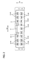
- FIG. 2 is a front view of the circuit board connector,
- FIG. 3 is a plan view of the circuit board connector,
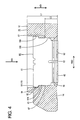
- FIG. 4 is a side view in section of the circuit board connector,
- FIG. 5 is a side view of a circuit board connector according to a second embodiment,
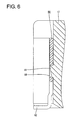
- FIG. 6 is a vertical section enlargedly showing a portion of the circuit board connector of FIG. 5, and
- FIG. 7 is a side view showing another embodiment.
- A first preferred embodiment of the present invention is described with reference to FIGS. 1 to 4. A circuit board connector of this embodiment is comprised of one or more, preferably a plurality of
terminal fittings 30, a connector housing in which the one or mroe respectiveterminal fittings 30 are at least partly mounted (hereinafter, merely "housing 10"), and one or more, preferably a pair of fixingportions 60 to be mounted in or to or on thehousing 10. Thehousing 10 is to be fixed to an electric or electronic device such as a circuit board K by means of the one ormore fixing portions 60 and is to be connected with an unillustrated mating housing. In the following description, a side to be connected with the mating connector is referred to as a front side, and reference is made to all the Figures except FIG. 3 concerning vertical direction. - The
housing 10 is made e.g. of a synthetic resin having a high heat resistance such as an LCP (liquid crystal polymer) or a PPS (polyphenylene sulfide), preferably substantially is laterally long as a whole, and includes aterminal holding portion 11 for holding theterminal fittings 30 and areceptacle 12 projecting substantially forward from or near the peripheral edge of theterminal holding portion 11 as shown in FIG. 2. - The
terminal holding portion 11 is formed with one or more, preferably a plurality of terminal insertion holes (not shown) into which the one or moreterminal fittings 30 can be at least partly inserted or pressed from an insertion side, preferably substantially from behind, to be mounted. Theterminal fittings 30 at least partly inserted or pressed into the terminal insertion holes are arranged at one or more stages, preferably at two (upper and lower) stages while being juxtaposed substantially along width direction WD and/or height direction HD (being arranged at an angle different from 0° or 180°, preferably substantially normal to the width direction WD). Threeterminal fittings 30 preferably are arranged at each of the lateral (left and right) sides of alock projection 13 to be described later at the upper stage, whereas nineterminals 30 are arranged at substantially even intervals substantially along width direction WD at the lower stage. At the opposite lateral (left and right) sides of theterminal holding portion 11, one or more, preferably a pair ofprotection walls 14 for protecting theterminal fittings 30 at least partly exposed at the rear surface of theterminal holding portion 11 are formed to substantially project outward or backward. - The
receptacle 12 preferably is substantially in the form of a rectangular tube having an open front side, and the mating housing is at least partly fittable thereinto substantially from front. The lateral (upper and lower) walls of thereceptacle 12 preferably are made thinner than those of theterminal holding portion 11 in order to reduce the height of thehousing 11. Thelock projection 13 engageable with an engaging portion of the mating housing to hold the two housings connected is formed in a widthwise preferably intermediate position (preferably substantially in the widthwise center) of the lateral (upper) wall of thereceptacle 12. One or more, preferably a pair of mountinggrooves 15 into which the one or more corresponding fixingportions 60 can be individually mounted are formed in the (preferably substantially opposite) side wall(s) (preferably substantially opposite widthwise sides) of thereceptacle 12. The construction of the mountinggrooves 15 is described in detail later together with the fixingportions 60. - The
terminal fittings 30 preferably are of a bent type, preferably substantially L-shaped as a whole, penetrate theterminal holding portion 11 while being substantially horizontally arranged in thereceptacle 12, have backward-projecting portions thereof bent at an angle different from 0° or 180°, preferably substantially normal or down at specified (predetermined or predeterminable) positions, and have the bottom ends thereof bent again at an angle different from 0° or 180°, preferably substantially normal to preferably extend substantially backward. A front portion (preferably substantially a front half) of eachterminal fitting 30 projecting in thereceptacle 12 is a connector-side connecting portion 31 connectable with a mating terminal arranged in the mating housing, whereas a rear portion (preferably substantially a rear half) thereof exposed at the rear surface of theterminal holding portion 11 is a board-side connecting portion 32 connectable with a conductor path provided at the electric or electronic device, preferably printed on the circuit board K, preferably by reflow soldering to be described later. Pairs of corresponding (upper and lower)terminal fittings 30 at different adjacent stages are displaced along transverse direction (or widthwise direction WD) after being drawn backward, whereby the board-side connecting portions 32 are arranged at substantially even intervals on the same straight line along transverse direction (or widthwise direction WD), and the rear ends thereof are substantially aligned at the substantially same position with respect to forward and backward directions FBD. - Each fixing
portion 60 is a peg-shaped (preferably metal) plate separate from thehousing 10 and is formed by punching or cutting a (preferably metal) sheet into a specified (predetermined or predeterminable) shape and applying bending to the cut-or punched-out (metal) sheet. More specifically, the fixingportion 60 is comprised of amain body 61 in the form of a substantially flat plate extending substantially along height direction HD (vertical direction) and a mounting orsolder portion 62 projecting at an angle different from 0° or 180°, preferably substantially normal to themain portion 61, preferably substantially sideways, from abottom end 66 of themain portion 61, and preferably is substantially L-shaped as a whole. The fixingportion 60 is cut in an intermediate position (preferably substantially in the middle) with respect to the width direction of the fixing portion 60 (forward and backward directions FBD) from thesolder portion 62 to an intermediate position along the height direction HD of themain portion 61, thereby forming aslit 63. Thesolder portion 62 is divided into a front and a rear areas at theslit 63. Even if either one of the front and rear areas comes to have a poor throwing power due to the thermal expansion of thehousing 10 to be described later, the influence thereof on the other side can be shut off or reduced by theslit 63. - On the other hand, each mounting
groove 15 into which the fixingportion 60 is at least partly mounted is formed to extend substantially in height direction HD and make openings preferably in both upper and bottom surfaces of thehousing 10, and is comprised of a main-body accommodating groove 16 into which the opposite lateral edges of themain portion 61 are at least partly insertable substantially along the plate surface of themain body 61, and a solder-portion accommodating groove 17 into which thesolder portion 62 is at an angle different from 0° or 180°, preferably substantially insertable along a direction at an angle different from 0° or 180°, preferably substantially normal to the plane surface thereof. - The
main portion 61 of each fixingportion 60 preferably is formed to have a stepped shape having two or more, e.g. three widths so that at least oneintermediate portion 65 is narrower than anupper end portion 64 and abottom end portion 66 is narrower than the intermediate portion(s) 65. Thesolder portion 62 preferably is formed to have substantially the same width as thebottom end portion 66 to which it is coupled. On the other hand, each main-portion accommodating groove 16 of the mountinggroove 15 preferably is formed such that awider portion 16A having a width substantially equal to or larger than that of theupper end portion 64 of themain body 61 and anarrower portion 16B having a width substantially equal to or larger than theintermediate portion 65 of themain portion 61 are connected one above the other, whereas the solder-portion accommodating groove 17 is formed to have a width substantially equal to or larger than those of thebottom end portion 66 of themain portion 61 and thesolder portion 62. - When the fixing
portion 60 is at least partly inserted into the mountinggroove 15, one or more steps 64a at the bottom end of theupper end portion 64 come substantially into contact with one or morerespective steps 16E at the bottom end of thewider portion 16A, whereby the fixingportion 60 is positioned with respect to thehousing 10. In this mounted state, specified (predetermined or predeterminable) clearances are defined between thebottom end portion 66 of themain portion 61 and thenarrower portion 16B. - Further, one or more, preferably a pair of retaining
portions 67 are formed to bulge out sideways at the (preferably substantially opposite) lateral edge(s) of theintermediate portion 65 of themain portion 61. The retainingportions 67 come to bite in or engage the groove edges of thenarrower portion 16B of the main-body accommodating groove 16, whereby the fixingportion 60 can be so held as not to come out of the mountinggroove 15. A projecting distance of thesolder portion 62 to the lateral side preferably is substantially equal to the depth of the solder-portion accommodating groove 17, so that the projecting end of thesolder portion 62 preferably is substantially in flush with the outer side surface of thehousing 10 in the mounted state. - The contact positions of the retaining
portions 67 with the groove edges of the mountinggroove 15 in the mounted state preferably are set at a lower level L2 located lower than, i.e. closer to the circuit board K than half the maximum height L1 (center) with respect to the height direction HD of the housing 10 (direction away from the circuit board K). In other words, these contact positions preferably are set within an area below the lower level L2 where the influence of the thermal expansion is relatively small when thehousing 10 thermally expands by heating. Thus, even if a separating force acts on thesolder portions 62 of the fixingportions 60 in the direction substantially away from the circuit board K e.g. as thehousing 10 thermally expands, thesolder portions 62 can be held solder-connected against this separating force. - Next, functions of this embodiment are described. First, the one or more respective
terminal fittings 30 are at least partly inserted into the corresponding terminal insertion holes of thehousing 10 from the inserting side, preferably substantially from behind. Subsequently, the one ormore fixing portions 60 are at least partly inserted into the one or more respective mountinggrooves 15 of thehousing 10 in a mounting direction MD (preferably substantially parallel to the height direction HD), preferably substantially from above, substantially along the plate surfaces of themain portions 61, wherein themain portions 61 are at least partly inserted into the main-portion accommodating grooves 16 and the solder-portions 62 are at least partly inserted into the solder-portion accommodating grooves 17. Such a mounting operation can be carried out e.g. using an unillustrated jig or the like. - Upon entering the
narrower portions 16B, theintermediate portions 65 are moved in the mounting direction MD; preferably substantially downward, while the retaining portion(s) 67 bite(s) in or engage(s) the groove edges of thenarrower portions 16B. Thesteps 64A of theupper end portions 64 come substantially into contact with thesteps 16E of thewider portions 16A after theupper end portions 64 at least partly enter thewider portions 16A, thereby preventing any further insertion of the fixingportions 60. In this state, the retainingportions 67 are located at the contact positions at the level L2 lower than half the maximum height L1 of the housing 10 (or in the lower half of thehousing 10 closer to the circuit board K), and bite in or engage the groove edges of thenarrower portions 16B corresponding to these contact positions, whereby the fixingportions 60 are prevented from coming out. It should be noted that theterminal fittings 30 may be mounted after the fixingportions 60 are mounted. - Subsequently, the
housing 10 having the fixingportions 60 mounted therein is to be fixed to the circuit board K (as a preferred electric or electronic device). To this end, solder is applied to lands on the outer surface of the circuit board K preferably beforehand, and thehousing 10 is placed on the circuit board K while the board-side connecting portions 32 of theterminal fittings 30 and thesolder portions 62 of the fixingportions 60 are brought substantially into contact with the corresponding lands. In this state, the circuit board K having thehousing 10 mounted thereon is caused to travel in a reflow furnace (not shown), thereby melting the solder to adhere the board-side connecting portions 32 and thesolder portions 62 to the corresponding lands. When the solder is cooled and solidified thereafter, theterminal fittings 30 are electrically connected with the conductor paths of the circuit board K and the fixingportions 60 are fixed to the circuit board K. - Here, the thermal expansion of the
housing 10 due to the heating in the reflow furnace is concerned. However, since thehousing 10 preferably is made of the resin having a high heat resistance in this embodiment, the thermal expansion coefficient of thehousing 10 can be held down even in a heated environment. Of course, if a lead-free solder is, for example, used, thehousing 10 needs to travel in the reflow furnace for a long time after the temperature of the reflow furnace is increased to melt the lead-free solder. Therefore, the influence of the thermal expansion of thehousing 10 is extended to the fixingportions 60, making it unignorable that a separating force acts on the fixingportions 60 in the direction substantially away from the circuit board K. - In this respect, the contact positions of the retaining
portions 67 with the groove edges of the mountinggrooves 15 preferably are set at the level L2 substantially lower than half the maximum height L1 of thehousing 10 along the height direction HD in this embodiment. Thus, an amount of thermal displacement can be held down without particularly accumulating amounts of displacement resulting from the thermal expansion (hereinafter, "amount of thermal displacement") from below (from the side of the circuit board K). As a result, amounts of thermal displacement of the fixingportions 60 can be held down, thereby making it possible to avoid a situation, for example, where the fixingportions 60 come to possess a poor throwing power with the solder to be separated from the circuit board K. - As described above, according to this embodiment, even if the separating force should act on the fixing
portions 60 in the direction away from the circuit board K due to the reflow soldering, a displacement restricting portion is formed by setting the contact positions of the retainingportions 67 with the groove edges of the mountinggrooves 15 at the lower level L2 near the circuit board K, thereby keeping the fixingportions 60 solder-connected against the separating force. Therefore, the separation of the fixingportions 60 from the circuit board K by becoming unsoldered can be prevented. - Accordingly, to satisfactorily keep a connected state of fixing portions, a circuit board connector is provided with one or
more fixing portions 60 for fixing a housing 10 (preferably made of a synthetic resin) to a circuit board K (as a preferred electric or electronic device). The fixingportions 60 preferably are made of a metal plate, and are to be connected with the circuit board K by soldering after being mounted into thehousing 10. Thehousing 10 is formed with one or more mountinggrooves 15 into which the fixingportions 60 are at least partly insertable, whereas the fixingportions 60 are formed with retainingportions 67 for biting in or engaging (preferably the edges of) the mountinggrooves 15 to prevent the fixingportions 60 from coming out of the mountinggrooves 15. Contact positions of the retainingportions 67 and the edges of the mountinggrooves 15 in a mounted state of the fixingportions 15 are set at a level L2 substantially lower (or substantially closer to the circuit board K) than half the maximum height L1 of thehousing 10. This serves as displacement restricting means for keeping the fixingportions 60 solder-connected with the circuit board K against a separating force when the separating force acts on the fixingportions 60 in a direction away from the circuit board K as thehousing 10 thermally expands. - Next, a second preferred embodiment of the present invention is described with reference to FIGS. 5 and 6. In the second embodiment, the aforementioned displacement restricting means is changed and the forms of the fixing
portions 60 and the mountinggrooves 15 differ those of the first embodiment. The others are similar or the same as in the first embodiment, and no repetitive description is given by identifying the same structural parts by the same reference numerals. - A locking hole or
recess 68 penetrates in thickness direction in an intermediate position (preferably substantially in the center) of themain portion 61 of (preferably each) fixingportion 60 with respect to width direction (forward and backward directions FBD) and/or height direction HD. On the other hand, on thehousing 10, a lockingprojection 18 closely fittable into the lockinghole 68 is formed on a surface of each mountinggroove 15 to substantially face the plate surface of themain portion 61. Only onelocking hole 68 is formed in one fixingportion 60, and thislocking hole 68 is engageable with one corresponding lockingprojection 18. - According to the second preferred embodiment, the fixing
portions 60 can be mounted into the mountinggrooves 15 of thehousing 10 by, more or less, pressing the lockingprojections 18 of thehousing 10 into the locking holes 68 of the fixingportions 60. At this time, the lockingprojection 18 and the lockinghole 68 are engaged only at one position for one fixingportion 60, areas where the fixingportions 60 are in contact with thehousing 10 can be maximally reduced. As a result, the influence of the thermal expansion of thehousing 10 on the fixingportions 60 can be reduced, enabling the connected state of the fixingportions 60 to be satisfactorily kept. - Since the engaged positions of the locking
projections 18 and the locking holes 68 preferably are set substantially in the widthwise centers of the fixingportions 60, the fixingportions 60 can be locked into thehousing 10 in well-balanced postures. Further, the lockingprojections 18 expand outward due to the thermal expansion of thehousing 10, thereby being brought into closer contact with the inner surfaces of the locking holes 68. Therefore, the fixingportions 60 are locked into thehousing 10 with a stronger force. - Contrary to the above, as shown in FIG. 7, a locking
projection 18A projecting inward may be formed on each fixingportion 60, a locking hole (not shown) is formed in the surface of each mountinggroove 15, and the fixingportion 60 may be locked into thehousing 10 by the engagement of the lockingprojection 18A and the locking hole. - The present invention is not limited to the above described and illustrated embodiments. For example, the following embodiments are also embraced by the technical scope of the present invention as defined by the claims. Beside the following embodiments, various changes can be made without departing from the scope and spirit of the present invention as defined by the claims.
- (1) According to the present invention, the displacement restricting means may be constructed by fixing the fixing portions by the known fixing means after being solder-connecting the fixing portions with the circuit board.
- (2) Although the terminal fittings are connected with the circuit board by soldering in the first and second embodiments, the present invention is also applicable to a circuit board connector using press-fit terminals whose board-side connecting portions are pressed into the circuit board for connection or insulation displacement terminal fittings being coonectable with conductors by insulation displacement. The forms of the terminal fittings are not limited to substantially L-shaped forms, and may be straight forms substantially linearly extending over the entire length or have any other bent shape. The present invention is also applicable to a circuit board connector, in a mating housing of which male terminal fittings are provided, wherein connector-side connecting portions are of the female type.
- (3) Although the contact positions of the retaining portions and the edges of the mounting grooves in the mounted state are set at positions closer to the circuit board than half the maximum height of the connector housing in the first embodiment, such contact positions may be set at positions located substantially just at half the maximum height of the connector housing.
- (4) According to the present invention, it is better to set the contact positions of the retaining portions and the edges of the mounting grooves in the mounted state maximally close to the circuit board by lowering them than in the first embodiment. This can more suppress the amounts of thermal displacements at the contact positions of the retaining portions and the edges of the mounting grooves, whereby the connected state of the fixing portions can be satisfactorily kept.
- (5) According to the present invention, only either one of the connection of the terminal fittings with the circuit board and that of the fixing portions with the circuit board may be done by reflow soldering, and the other may be done by manual soldering or the like.
- (6) A heat source for causing the thermal expansion of the housing is not limited to the reflow furnace, and the present invention is widely applicable in cases where the entire housing is exposed to an environment subject to temperature fluctuations.
- (7) Even though the invention has been described with respect to a connector mountable to a printed circuit board, it should be understood that the invention is applicable to other types of connectors mountable to electric or electronic devices such as flexible circuit boards, junction boxes, airbag devices, dashboard circuits, etc.
-
- 10 ...
- housing (connector housing)
- 12 ...
- receptacle
- 15 ...
- mounting groove
- 18, 18A ...
- locking projection (displacement restricting means)
- 60 ...
- fixing portion
- 61 ...
- main portion
- 62 ...
- solder portion
- 67 ...
- retaining portion (displacement restricting means)
- 68 ...
- locking hole or recess (displacement restricting means)
- L1 ...
- maximum height of the connector housing
Claims (11)
- A connector mountable on an electric or electronic device such as a printed circuit board (K), comprising at least one fixing portion (60) for fixing a connector housing (10) to an electric or electronic device such as a circuit board (K), wherein:the fixing portion (60) is made of a metal plate and is connected with the electric or electronic device (K) by soldering after being mounted into or on the connector housing (10), andone or more displacement restricting means (67; 18, 68; 18A) for keeping the fixing portion (60) solder-connected with the electric or electronic device (K) against a separating force when the separating force acts on the fixing portion (60) in a direction substantially away from the electric or electronic device (K) as the connector housing (10) thermally expands is provided between the connector housing (10) and the fixing portion (60).
- A connector according to claim 1, wherein:the connector housing (10) is formed with a mounting groove (15) into which the fixing portion (60) is at least partly insertable.
- A connector according to one or more of the preceding claims, wherein the fixing portion (60) is formed with a retaining portion (67) for biting in an edge of the connector housing (10), preferably of the mounting groove (15), to prevent the fixing portion (60) from separating from the connector housing (10), preferably from coming out of the mounting groove (15).
- A connector according to claim 3, wherein a contact position of the retaining portion (67) and the edge of the mounting groove (15) in a mounted state of the fixing portion (60) is set to be substantially equal to or lower (L2) than about half the maximum height (L1) of the connector housing (10) with respect to the direction (HD) away from the electric or electronic device (K), thereby constructing at least part of the displacement restricting means (67; 18, 68; 18A).
- A connector according to claim 4, wherein the contact position of the retaining portion (67) and the edge of the mounting groove (15) in the mounted state is set at a position in proximity to the electric or electronic device (K).
- A connector according to one or more of the preceding claims, wherein:the displacement restricting means (67; 18, 68; 18A) comprises:wherein the fixing portion (60) can be locked into the connector housing (10) by the recess-projection engagement of the engaging portion (18; 18A) and the locking portion (68).at least one locking portion (18; 18A) being formed at the connector housing (10),at least one engaging portion (68) being formed at the fixing portion (60),
- A connector according to claim 6, wherein the engaging portion (68) and the locking portion (18; 18A) are engaged only at one position for one fixing portion (60).
- A connector according to claim 6 or 7, wherein the engaging portion (68) and the locking portion (18; 18A) are set substantially corresponding to the widthwise center of the fixing portion (60).
- A connector according to claim 6, 7 or 8, wherein the engaging portion (68) comprises a locking hole or recess penetrating the fixing portion (60) in thickness direction, and the locking portion (18; 18A) comprises a locking projection (18; 18A) at least partly fittable into the locking hole (68).
- A connector according to one or more of the preceding claims, wherein the fixing portion (60) has a diverging or step-wise configuration gradually becoming larger towards a rear part as seen in a mounting direction (MD) of the fixing portion (60) to the connector housing (10).
- A connector according to one or more of the preceding claims, wherein the connector housing (10) is made of a synthetic resin preferably having a high heat resistance such as an liquid crystal polymer (LCP) or a polyphenylene sulfide (PPS).
Applications Claiming Priority (1)
| Application Number | Priority Date | Filing Date | Title |
|---|---|---|---|
| JP2005148036A JP4560727B2 (en) | 2005-05-20 | 2005-05-20 | Board connector |
Publications (1)
| Publication Number | Publication Date |
|---|---|
| EP1724879A1 true EP1724879A1 (en) | 2006-11-22 |
Family
ID=36738742
Family Applications (1)
| Application Number | Title | Priority Date | Filing Date |
|---|---|---|---|
| EP06010206A Withdrawn EP1724879A1 (en) | 2005-05-20 | 2006-05-17 | A connector to be mounted on an electric/electronic device |
Country Status (3)
| Country | Link |
|---|---|
| US (1) | US7267577B2 (en) |
| EP (1) | EP1724879A1 (en) |
| JP (1) | JP4560727B2 (en) |
Families Citing this family (5)
| Publication number | Priority date | Publication date | Assignee | Title |
|---|---|---|---|---|
| JP5834243B2 (en) * | 2011-09-09 | 2015-12-16 | パナソニックIpマネジメント株式会社 | Holding bracket, connector connector and connector |
| JP6528647B2 (en) * | 2015-10-30 | 2019-06-12 | 住友電装株式会社 | Board connector |
| JP6997951B2 (en) | 2018-03-26 | 2022-01-18 | 住友電装株式会社 | Board connector |
| JP7245432B2 (en) * | 2019-09-19 | 2023-03-24 | 住友電装株式会社 | connector |
| CN112904066B (en) * | 2021-04-08 | 2022-09-27 | 扬州万泰电子科技有限公司 | Anti-theft intelligent electric meter |
Citations (9)
| Publication number | Priority date | Publication date | Assignee | Title |
|---|---|---|---|---|
| US5120256A (en) * | 1991-07-16 | 1992-06-09 | Walden John D | Retention system for a connector housing |
| EP0613217A1 (en) * | 1993-02-23 | 1994-08-31 | Molex Incorporated | Retention system for circuit board mounted electrical connector |
| US5449297A (en) * | 1992-03-06 | 1995-09-12 | Augat Inc. | Edge card connector |
| US6129589A (en) * | 1998-11-24 | 2000-10-10 | Molex Incorporated | Terminal retention system |
| EP1198031A2 (en) * | 2000-10-13 | 2002-04-17 | Autonetworks Technologies, Ltd. | Connector with reinforcing structure for securing the connector housing to a circuit board |
| WO2003058766A1 (en) * | 2001-12-28 | 2003-07-17 | Matsushita Electric Works, Ltd. | Connector with switching function |
| US20050026481A1 (en) * | 2003-07-31 | 2005-02-03 | Atsushi Nishio | Connector provided with shutter |
| EP1538706A2 (en) * | 2003-12-03 | 2005-06-08 | Sumitomo Wiring Systems, Ltd. | A connector fixing bracket |
| EP1587170A1 (en) * | 2004-04-12 | 2005-10-19 | Sumitomo Wiring Systems, Ltd. | A connector and a method of mounting it |
Family Cites Families (8)
| Publication number | Priority date | Publication date | Assignee | Title |
|---|---|---|---|---|
| DE3431814A1 (en) | 1984-08-30 | 1986-03-06 | Werner Grüske, EDV Zubehör, 8521 Spardorf | DEVICE FOR THE ORDERLY STORAGE OF A LARGER NUMBER OF RECORDING CARRIERS |
| WO1993002489A1 (en) * | 1991-07-16 | 1993-02-04 | E.I. Du Pont De Nemours And Company | Retention system for a connector housing |
| JPH0587839U (en) * | 1991-07-30 | 1993-11-26 | ミツミ電機株式会社 | Modular jack |
| JPH07240246A (en) * | 1994-02-28 | 1995-09-12 | Amp Japan Ltd | Board mounted electrical connector |
| TW461631U (en) * | 2000-10-09 | 2001-10-21 | Hon Hai Prec Ind Co Ltd | Electrical connector |
| US6645005B2 (en) * | 2001-11-29 | 2003-11-11 | Hon Hai Precision Ind. Co., Ltd. | Electrical connector assembly with latching metal ears |
| JP2005294163A (en) * | 2004-04-02 | 2005-10-20 | Jst Mfg Co Ltd | Electrical connector with reinforcing tab |
| US7001212B1 (en) * | 2005-01-21 | 2006-02-21 | Hon Hai Precision Ind. Co., Ltd. | Surface mountable retention bracket for electrical connector |
-
2005
- 2005-05-20 JP JP2005148036A patent/JP4560727B2/en not_active Expired - Fee Related
-
2006
- 2006-05-17 US US11/435,591 patent/US7267577B2/en not_active Expired - Fee Related
- 2006-05-17 EP EP06010206A patent/EP1724879A1/en not_active Withdrawn
Patent Citations (9)
| Publication number | Priority date | Publication date | Assignee | Title |
|---|---|---|---|---|
| US5120256A (en) * | 1991-07-16 | 1992-06-09 | Walden John D | Retention system for a connector housing |
| US5449297A (en) * | 1992-03-06 | 1995-09-12 | Augat Inc. | Edge card connector |
| EP0613217A1 (en) * | 1993-02-23 | 1994-08-31 | Molex Incorporated | Retention system for circuit board mounted electrical connector |
| US6129589A (en) * | 1998-11-24 | 2000-10-10 | Molex Incorporated | Terminal retention system |
| EP1198031A2 (en) * | 2000-10-13 | 2002-04-17 | Autonetworks Technologies, Ltd. | Connector with reinforcing structure for securing the connector housing to a circuit board |
| WO2003058766A1 (en) * | 2001-12-28 | 2003-07-17 | Matsushita Electric Works, Ltd. | Connector with switching function |
| US20050026481A1 (en) * | 2003-07-31 | 2005-02-03 | Atsushi Nishio | Connector provided with shutter |
| EP1538706A2 (en) * | 2003-12-03 | 2005-06-08 | Sumitomo Wiring Systems, Ltd. | A connector fixing bracket |
| EP1587170A1 (en) * | 2004-04-12 | 2005-10-19 | Sumitomo Wiring Systems, Ltd. | A connector and a method of mounting it |
Also Published As
| Publication number | Publication date |
|---|---|
| JP2006324189A (en) | 2006-11-30 |
| US7267577B2 (en) | 2007-09-11 |
| JP4560727B2 (en) | 2010-10-13 |
| US20060264097A1 (en) | 2006-11-23 |
Similar Documents
| Publication | Publication Date | Title |
|---|---|---|
| US9590327B2 (en) | Reinforcing metal fitting and a connector having the reinforcing metal fitting | |
| US7134886B2 (en) | Connector and terminal fitting | |
| US6866523B2 (en) | Construction for mounting a terminal, a circuit board connector and method of mounting it | |
| US7094100B2 (en) | Connector and method of mounting it | |
| JP3013756B2 (en) | Board connector | |
| US10998655B2 (en) | Connector and connection system | |
| US7708605B2 (en) | Connector with terminal fittings press fit in a base wall of a connector housing | |
| CN101032057B (en) | board connector | |
| US7806702B2 (en) | Connector for an electric device such as a board | |
| EP1993173B1 (en) | A set of circuit board connectors and a method of mounting a connector to a circuit board | |
| EP1538706B1 (en) | A connector fixing bracket | |
| US7458848B2 (en) | Connector | |
| US7077694B2 (en) | Connector to be fixed to a device and method of fixing a connector to a device | |
| JP4103788B2 (en) | Board connector | |
| US7267577B2 (en) | Connector to be mounted on an electric/electronic device | |
| EP1768217B1 (en) | A connector and connector assembly | |
| US7207837B2 (en) | Connector and a mounting method therefor | |
| KR102143973B1 (en) | Connector | |
| JP5517999B2 (en) | Surface mount connector | |
| US20240154328A1 (en) | Board connector and electrical device | |
| US20240063563A1 (en) | Sheet-like conductive path | |
| CN107112669A (en) | Connector | |
| JPH0773940A (en) | Electrical connector | |
| JPH10321313A (en) | Structure of narrow pitch connector |
Legal Events
| Date | Code | Title | Description |
|---|---|---|---|
| PUAI | Public reference made under article 153(3) epc to a published international application that has entered the european phase |
Free format text: ORIGINAL CODE: 0009012 |
|
| 17P | Request for examination filed |
Effective date: 20060524 |
|
| AK | Designated contracting states |
Kind code of ref document: A1 Designated state(s): AT BE BG CH CY CZ DE DK EE ES FI FR GB GR HU IE IS IT LI LT LU LV MC NL PL PT RO SE SI SK TR |
|
| AX | Request for extension of the european patent |
Extension state: AL BA HR MK YU |
|
| AKX | Designation fees paid |
Designated state(s): DE FR |
|
| 17Q | First examination report despatched |
Effective date: 20091103 |
|
| GRAP | Despatch of communication of intention to grant a patent |
Free format text: ORIGINAL CODE: EPIDOSNIGR1 |
|
| RIN1 | Information on inventor provided before grant (corrected) |
Inventor name: OKAMURA, KENJI C/O SUMITOMO WIRING SYSTEMS, LTD. Inventor name: NAKANO, HIROSHICO/ SUMITOMO WIRING SYSTEMS, LTD. |
|
| STAA | Information on the status of an ep patent application or granted ep patent |
Free format text: STATUS: THE APPLICATION IS DEEMED TO BE WITHDRAWN |
|
| 18D | Application deemed to be withdrawn |
Effective date: 20101108 |