EP1538706B1 - A connector fixing bracket - Google Patents
A connector fixing bracket Download PDFInfo
- Publication number
- EP1538706B1 EP1538706B1 EP04028607A EP04028607A EP1538706B1 EP 1538706 B1 EP1538706 B1 EP 1538706B1 EP 04028607 A EP04028607 A EP 04028607A EP 04028607 A EP04028607 A EP 04028607A EP 1538706 B1 EP1538706 B1 EP 1538706B1
- Authority
- EP
- European Patent Office
- Prior art keywords
- portions
- connector
- board
- circuit board
- housing
- Prior art date
- Legal status (The legal status is an assumption and is not a legal conclusion. Google has not performed a legal analysis and makes no representation as to the accuracy of the status listed.)
- Expired - Fee Related
Links
- 238000005476 soldering Methods 0.000 claims description 50
- 229910000679 solder Inorganic materials 0.000 claims description 34
- 230000008878 coupling Effects 0.000 claims description 19
- 238000010168 coupling process Methods 0.000 claims description 19
- 238000005859 coupling reaction Methods 0.000 claims description 19
- 239000002184 metal Substances 0.000 claims description 14
- 238000003466 welding Methods 0.000 claims description 7
- 238000003780 insertion Methods 0.000 description 46
- 230000037431 insertion Effects 0.000 description 46
- 230000013011 mating Effects 0.000 description 17
- 239000004020 conductor Substances 0.000 description 8
- 230000002093 peripheral effect Effects 0.000 description 7
- 238000005452 bending Methods 0.000 description 6
- 238000004049 embossing Methods 0.000 description 5
- 239000000463 material Substances 0.000 description 5
- 238000005520 cutting process Methods 0.000 description 4
- 238000010276 construction Methods 0.000 description 3
- 239000012212 insulator Substances 0.000 description 3
- 230000002411 adverse Effects 0.000 description 2
- 230000001419 dependent effect Effects 0.000 description 1
- 238000004519 manufacturing process Methods 0.000 description 1
- 238000000034 method Methods 0.000 description 1
- 230000003252 repetitive effect Effects 0.000 description 1
Images


Classifications
-
- H—ELECTRICITY
- H01—ELECTRIC ELEMENTS
- H01R—ELECTRICALLY-CONDUCTIVE CONNECTIONS; STRUCTURAL ASSOCIATIONS OF A PLURALITY OF MUTUALLY-INSULATED ELECTRICAL CONNECTING ELEMENTS; COUPLING DEVICES; CURRENT COLLECTORS
- H01R13/00—Details of coupling devices of the kinds covered by groups H01R12/70 or H01R24/00 - H01R33/00
- H01R13/46—Bases; Cases
-
- H—ELECTRICITY
- H01—ELECTRIC ELEMENTS
- H01R—ELECTRICALLY-CONDUCTIVE CONNECTIONS; STRUCTURAL ASSOCIATIONS OF A PLURALITY OF MUTUALLY-INSULATED ELECTRICAL CONNECTING ELEMENTS; COUPLING DEVICES; CURRENT COLLECTORS
- H01R4/00—Electrically-conductive connections between two or more conductive members in direct contact, i.e. touching one another; Means for effecting or maintaining such contact; Electrically-conductive connections having two or more spaced connecting locations for conductors and using contact members penetrating insulation
- H01R4/02—Soldered or welded connections
- H01R4/028—Soldered or welded connections comprising means for preventing flowing or wicking of solder or flux in parts not desired
-
- H—ELECTRICITY
- H01—ELECTRIC ELEMENTS
- H01R—ELECTRICALLY-CONDUCTIVE CONNECTIONS; STRUCTURAL ASSOCIATIONS OF A PLURALITY OF MUTUALLY-INSULATED ELECTRICAL CONNECTING ELEMENTS; COUPLING DEVICES; CURRENT COLLECTORS
- H01R12/00—Structural associations of a plurality of mutually-insulated electrical connecting elements, specially adapted for printed circuits, e.g. printed circuit boards [PCB], flat or ribbon cables, or like generally planar structures, e.g. terminal strips, terminal blocks; Coupling devices specially adapted for printed circuits, flat or ribbon cables, or like generally planar structures; Terminals specially adapted for contact with, or insertion into, printed circuits, flat or ribbon cables, or like generally planar structures
- H01R12/70—Coupling devices
- H01R12/7005—Guiding, mounting, polarizing or locking means; Extractors
- H01R12/7011—Locking or fixing a connector to a PCB
- H01R12/707—Soldering or welding
-
- H—ELECTRICITY
- H01—ELECTRIC ELEMENTS
- H01R—ELECTRICALLY-CONDUCTIVE CONNECTIONS; STRUCTURAL ASSOCIATIONS OF A PLURALITY OF MUTUALLY-INSULATED ELECTRICAL CONNECTING ELEMENTS; COUPLING DEVICES; CURRENT COLLECTORS
- H01R13/00—Details of coupling devices of the kinds covered by groups H01R12/70 or H01R24/00 - H01R33/00
- H01R13/40—Securing contact members in or to a base or case; Insulating of contact members
- H01R13/405—Securing in non-demountable manner, e.g. moulding, riveting
- H01R13/41—Securing in non-demountable manner, e.g. moulding, riveting by frictional grip in grommet, panel or base
-
- H—ELECTRICITY
- H01—ELECTRIC ELEMENTS
- H01R—ELECTRICALLY-CONDUCTIVE CONNECTIONS; STRUCTURAL ASSOCIATIONS OF A PLURALITY OF MUTUALLY-INSULATED ELECTRICAL CONNECTING ELEMENTS; COUPLING DEVICES; CURRENT COLLECTORS
- H01R43/00—Apparatus or processes specially adapted for manufacturing, assembling, maintaining, or repairing of line connectors or current collectors or for joining electric conductors
- H01R43/02—Apparatus or processes specially adapted for manufacturing, assembling, maintaining, or repairing of line connectors or current collectors or for joining electric conductors for soldered or welded connections
- H01R43/0256—Apparatus or processes specially adapted for manufacturing, assembling, maintaining, or repairing of line connectors or current collectors or for joining electric conductors for soldered or welded connections for soldering or welding connectors to a printed circuit board
Definitions
- the present invention relates to a connector which is to be connected or mounted on an electric or electronic device such as a circuit board (so-called circuit board connector).
- circuit board connector is e.g. known from Japanese Unexamined Patent Publication No. H05-326049 .
- board fixing portions 4 bulging sideways are integrally formed at the bottom ends of the opposite side surfaces of the housing 2, and screws 6 inserted through screw insertion holes formed in the circuit board 3 are driven into screw holes 5 formed in the board fixing portions 4.
- the board fixing portions 4 need to have a certain size or larger in order to maintain strength, which leads to a tendency to enlarge the entire circuit board connector.
- circuit board connector is known from Japanese Unexamined Patent Publication No. H06-325826 .
- base portions of terminal fittings are inserted and held in a housing, portions of the terminal fittings projecting backward from the housing are bent down, and the bottom ends of these portions serve as board-side connecting portions to be electrically connected with a circuit board by soldering.
- a plurality of terminal fittings are arranged side by side along widthwise direction.
- US-A-6 089 883 discloses an electric connector assembly comprising a pair of plug and receptacle board-to-board connectors.
- Each connector has an insulative housing with a plurality of contacts wherein each contact has substantially a cantilever type spring arm with a maximum deflection apex thereof. Mated plug and receptacle connectors pass the maximum deflection apexes of the contacts with each other to provide positive locking thereof.
- Each connector further includes a grounding plate longitudinally extending along the housing wherein coupling means are formed respectively on the grounding plate of each connector for combining such pair of grounding plates together.
- a pair of mounting devices is disposed adjacent two opposite ends of the housing of each connector and mechanically and electrically engaged with the respective distal ends of the corresponding grounding plate in the same connector.
- EP-A-0 789 422 discloses an anti-wicking system for electrical connectors.
- the anti-wicking system is provided in an electrical connector adapted for mounting on a printed circuit board having solderable circuit traces thereon.
- the connector includes a housing having a plurality of terminal-receiving passages. A plurality of terminals are inserted into the passages, with solder tail portions of the terminals projecting from the housing for solder connection to the circuit traces on the printed circuit board.
- the housing has at least one projecting portion adjacent the terminals to provide extra housing material which can be heat staked about the terminals to prevent solder wicking therealong.
- US-A-5 362 256 discloses a connector which is capable of arranging a large number of contacts in an insulator with high density.
- the connector includes a plurality of leaf contacts and an insulator for holding the contacts.
- the contact comprises a fixed portion fixed to the insulator, an elastic spring portion integrally connected to one end of the fixed portion, and a contact portion integrally connected to one end of the elastic spring portion and being offset from a surface of the fixed portion and the elastic spring portion.
- the present invention was developed in view of the above problem and an object thereof is to miniaturize a connector for an electric or electronic device such as a circuit board.
- a connector for mounting to an electric device particularly being circuit board connector comprising:
- a circuit board connector comprising:
- the board fixing portion made of a metal plate is mounted into the connector housing and fixed to the circuit board by soldering, the board fixing portion can be made smaller as compared to a prior art one for fixing a connector housing by means of screw(s). Thus, the entire circuit board connector can be miniaturized.
- the molten solder Even if an excessive amount of molten solder is used to fix the board fixing portion, the molten solder at least partly flows or can flow into the solder inflow space. This can prevent the molten solder from flowing onto the circuit board.
- a plurality of (board) fixing portions are coupled substantially side by side to a carrier via coupling portions, and the board fixing portion is at least partly mounted into the connector housing after being cut off from the carrier at the coupling portion, and
- a soldering portion to be soldered to the circuit board preferably is provided at an end of the (board) fixing portion different from an end thereof where the coupling portion is provided.
- soldering portion is provided at the end of the (board) fixing portion different from the one where the coupling portion is provided, even if burrs are formed upon cutting the coupling portion, these burrs can be prevented from adversely affecting the soldering.
- the connector housing is formed with at least one mount groove into which the (board) fixing portion is at least partly insertable, and the (board) fixing portion comprises at least one retaining portion for retaining the (board) fixing portion in the mount groove particularly by biting into or engaging a groove edge of the mount groove, and preferably at least one arm portion resiliently deformable to bring the retaining portion away from the groove edge of the mount groove.
- a circuit board connector shown in this embodiment is comprised of one or more, preferably a plurality of terminal fittings 20, a connector housing 10 (hereinafter, merely housing 10") into which the respective one or more terminal fittings 20 are at least partly mountable, and one or more, preferably a pair of board fixing portions 30 mountable into or onto the housing 10.
- the housing 10 is to be fixed to a circuit board K (as a preferred electric or electronic device) by means of the board fixing portions 30 and is connectable with an unillustrated mating housing.
- a side of the housing 10 to be connected with the mating housing (right side in FIG. 3) is referred to as front side, and reference is made to all the figures except FIG. 4 concerning vertical direction.
- the housing 10 preferably is substantially laterally long as a whole and includes a terminal holding portion 11 in which the terminal fittings 20 can be held and preferably a receptacle 12 projecting forward from or at the peripheral edge or edge portion of the terminal holding portion 11.
- the terminal holding portion 11 is formed with one or more, preferably a plurality of terminal insertion holes 13 into which the terminal fittings 20 are at least partly insertable from an inserting side, preferably substantially from behind.
- the respective terminal insertion holes 13 are arranged substantially side by side along widthwise direction WD at one or more stages, preferably at two (upper and lower) stages.
- terminal insertion holes 13 are arranged at the lower or first stage and eighteen terminal insertion holes 13 are arranged at the upper or second stage. Particularly, nine terminal insertion holes are arranged at each of the left and rights of the upper stage shown in FIG. 1.
- the terminal insertion holes 13 at the upper stage and those at the lower stage are at positions displaced (offset) along widthwise direction WD.
- the receptacle 12 preferably is substantially in the form of a rectangular tube having an open front end, and the mating housing is at least partly fittable thereinto from a mating side or substantially from front.
- At least one lock portion 14 engageable with at least one respective lock arm of the mating housing to hold the two housings connected projects downward (inward) at an intermediate position (preferably at a substantially widthwise middle position) of the upper part of the receptacle 12.
- a mount groove 15 into which the board fixing portion 30 is individually mountable is provided at each of the opposite widthwise ends of the receptacle 12 (housing 10). The structure of the mounting grooves 15 is described in detail later together with the board fixing portions 30.
- each terminal fitting 20 projecting backward from the terminal holding portion 11 is bent at an angle different from 0° or 180°, preferably substantially normal or down at a specified (predetermined or predeterminable) position, and the distal or bottom end of this bent or bent-down portion preferably is bent again to extend substantially backward or substantially parallel to a connector-side connecting portion 21.
- a portion of each terminal fitting 20 projecting forward from the front surface (connecting surface) of the terminal holding portion 11 and preferably at least partly surrounded by the receptacle 12 serves as the connector-side connecting portion 21 electrically connectable with a mating terminal arranged in the mating housing.
- the rear end of the terminal fitting 20 serves as a board-side connecting portion 22 to be electrically connected with the electric or electronic device, preferably with a conductor path (not shown) printed on the circuit board K e.g. by soldering, welding, ultrasonic welding, press-fitting, etc.
- the terminal fittings 20 mounted in the housing 10 the terminal fittings 20 at the upper or second stage are offset from those at the lower or first stage along widthwise direction WD and/or the board-side connecting portions 22 of the terminal fittings 20 at both (upper and lower) stages are located substantially at the same position with respect to forward and backward directions FBD (or a direction at an angle different from 0° or 180°, preferably substantially normal to the widthwise direction WD) as shown in FIGS. 2 to 4.
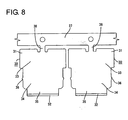
- Each board fixing portion 30 preferably is made of a (preferably metal) plate separate from the housing 10 and formed by applying bending, folding and/or embossing and the like to a (metal) plate material stamped or cut out into a specific (predetermined or predeterminable) shape as shown in FIGS. 4 to 7.
- the board fixing portion 30 is comprised of a main portion 31 substantially in the form of a flat plate extending or to be arranged (in use) substantially along vertical direction VD (or a direction at an angle different from 0° or 180°, preferably substantially normal to the widthwise direction WD and/or the forward and backward directions FBD) and a connecting or soldering portion 32 projecting laterally from a bottom or lateral end 35 of the main portion 31 to be arranged substantially along widthwise direction WD, and preferably is substantially L-shaped as a whole when viewed from front or behind (see FIG. 7).
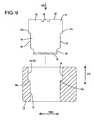
- the mount groove 15 into which this board fixing portion 30 is mountable is comprised of a main-portion accommodating portion 16 into which the main portion 31 is at least partly insertable along a direction of its plate surface, and a connecting- or soldering-portion accommodating portion 17 into which the connecting or soldering portion 32 is at least partly insertable substantially along a direction normal (or substantially along the forward and backward directions FBD) to a direction of its plate surface (or substantially normal to the vertical direction VD).
- the main portion 31 of the board fixing portion 30 has such a converging or stepped outer configuration as to have two or more, preferably three widths narrowed from an upper portion 33 (large-width portion) to a middle portion 34 (middle-width portion) to a bottom portion 35 (small-width portion) in this order, and the soldering portion 32 preferably is formed to have substantially the same width as the bottom portion 35 to which the soldering portion 32 is coupled.
- the main-portion accommodating portion 16 of the mount groove 15 is such that a wider portion 18 having a width substantially equal to or larger than the upper portion 33 of the main portion 31 and a narrower portion 19 having a width substantially equal to or larger than the middle portion 34 of the main portion 31 are vertically coupled or arranged close to each other, whereas the soldering-portion accommodating portion 17 is formed to have a width substantially equal to or larger than the bottom portion 35 of the main portion 31 and the soldering portion 32.
- a step or narrowed portion 33a at the bottom end of the upper portion 33 of the main portion 31 comes substantially into contact with a step or narrowed portion 18a at the bottom end of the wider portion 18 of the main-portion accommodating portion 16, whereby the bottom surface of the board fixing portion 30 preferably is so positioned as to be substantially in flush with the bottom surface of the housing 10.
- the bottom portion 35 of the main portion 31 is spaced from the narrower portion 19 of the main-portion accommodating portion 16 by specified (predetermined or predeterminable) clearances, which serve as solder inflow spaces S that are laterally exposed to the outside and permits the at least partial flow or entrance of the solder (as a preferred connecting means) during a connecting or soldering operation.
- one or more notches 17a are formed at the bottom or distal ends of the groove edges of the soldering-portion accommodating portion 17 in order to facilitate the at least partial inflow of the solder (see FIG. 5).
- One or more, preferably a pair of retaining portions 36 laterally project from the opposite side edges preferably of the middle portion 34 of the main portion 31.
- the retaining portions 36 bite into or engage the groove edges of the narrower portion 19 of the main-portion accommodating portion 16 to retain the board fixing portion 30 in the mount groove 15. Since a projecting distance of the soldering portion 32 is set to be substantially equal to the depth of the soldering-portion accommodating portion 17, the projecting end of the soldering portion 32 preferably is substantially in flush with the outer side surface of the housing 10 with the board fixing portion 30 at least partly mounted in the mount groove 15.
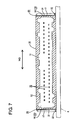
- a plurality of board fixing portions 30 preferably are (temporarily) coupled substantially side by side to a carrier 37 extending in the widthwise direction of the board fixing portions 30 (see FIG. 8). More specifically, the respective board fixing portions 30 are coupled to the carrier 37 via coupling portions 38 formed at the upper ends (ends opposite (different) from the soldering portions 32) of the main portions 31, and the coupling portions 38 are cut to separate the board fixing portions 30 from the carrier 37 upon or after or before mounting the board fixing portions 30 into the housing 10.
- chained board fixing portions as shown in FIG. 8 are formed by stamping or cutting a (preferably metal) blank out and bending, folding and/or embossing the soldering portions 32, the respective coupling portions 38 are cut at their intermediate positions (substantially same positions as the upper end positions of the main portions 31) to separate the respective board fixing portions 30 from the carrier 37.
- the respective terminal fittings 20 are at least partly inserted into the terminal insertion holes 13 of the housing 10 preferably substantially from behind to be mounted.
- the board fixing portions 30 are at least partly mounted into the housing 10.
- the board fixing portions 30 are at least partly inserted into the mount grooves 15 in a mounting direction MD (preferably from above or substantially along the vertical direction VD) substantially along the direction of the plate surfaces of the main portions 31 from a state shown in FIGS. 9 and 10, the main portions 31 and the soldering portions 32 at least partly enter the main-portion accommodating portions 16 and the soldering-portion accommodating portions 17, respectively.
- the upper ends (ends toward the coupling portions 38) of the main portions 31 preferably are pushed by an unillustrated jig.
- the middle portions 34 move substantially in the mounting direction MD or downward while the retaining portions 36 bite into or engage the groove edges of the narrower portions 19.
- the steps 33 of the upper portions 33 come substantially into contact with the steps 18a of the wider portions 18 as shown in FIGS. 6 and 7, whereby any further insertion of the board fixing portions 30 in the mounting direction MD can be prevented.
- the bottom end surfaces of the main portions 31 and the soldering portions 32 preferably are so positioned as to be substantially in flush with the bottom end surface of the housing 10.
- the retaining portions 36 bite in or engage the groove edges of the narrower portions 19, thereby preventing the board fixing portions 30 from coming (upward) out of the mount grooves 15. It does not matter even if the terminal fittings 20 are mounted after the board fixing portions 30 are mounted.
- the housing 10 having one or more, preferably both board fixing portions 30 at least partly mounted therein is or is to be fixed to the circuit board K (as the preferred electric or electronic device).
- the housing 10 is at least partly placed substantially on the circuit board K and the soldering portions 32 of both board fixing portions 30 are disposed at or near positions of the circuit board K planned to fix the soldering portions 32, molten solder is attached to the peripheral edges of the soldering portions 32.
- the molten solder at least partly flows into the solder inflow spaces S defined between the bottom portions 35 of the main portions 31 and the narrower portions 19 of the main-portion accommodating portions 16. This can prevent the molten solder from flowing onto the circuit board K.
- the board fixing portions 30 are fixed to the circuit board K by solidifying the attached solder.
- the respective terminal fittings 20 are successively soldered.
- the board-side connecting portions 22 of the respective terminal fittings 20 are laid substantially on or near the corresponding conductor paths on the circuit board K, and the molten solder is attached to the peripheral edges of the board-side connecting portions 22.
- the board-side connecting portions 22 are fixed to the circuit board K while being electrically connected with the conductor paths. It does not matter even if the board fixing portions 30 are fixed to the circuit board K after the terminal fittings 20 are soldered. Even in such a case, the soldering operation can be successively carried out.
- the board fixing portions 30 made of a metal plate are mounted into the housing 10 and are fixed to the circuit board K by soldering.
- the board fixing portions 30 can be made smaller, with the result that the entire circuit board connector can be miniaturized.
- the operation of fixing the board fixing portions 30 and the operation of soldering the terminal fittings 20 can be successively carried out in addition to being unnecessary to tighten up screws as with the prior art, operability is better.
- solder inflow spaces S are at least partly defined between the board fixing portions 30 and the housing 10, the redundant solder at least partly flows or can at least partly flow into the solder inflow spaces S even if an amount of the molten solder is excessive upon soldering the board fixing portions 30. Therefore, the solder can be advantageously prevented from flowing onto the circuit board K.
- soldering portion 32 is provided at the end or side of the board fixing portion 30 different from the end where the coupling portion 38 is provided, even if burrs are formed as the coupling portion 38 is cut, they can be prevented from adversely affecting the soldering.
- the terminal fittings 20 at the upper stage and those at the lower stage are offset along widthwise direction WD and/or the board-side connecting portions 22 of the terminal fittings 20 at the upper and lower stages are located substantially at the same position with respect to forward and backward directions FBD. Accordingly, as compared to circuit board connectors that tend to be long along forward and backward directions by arranging board-side connecting portions of terminal fittings at upper and lower stages in an offset manner along forward and backward directions, the entire circuit board connector can be made smaller along forward and backward directions.
- a housing 10 is formed with one or more mount grooves 15 into which board fixing portions 30 made of a metal plate are at least partly mountable.
- Each board fixing portion 30 is comprised of a main portion 31 and a soldering portion 32 (as a preferred connecting portion) projecting laterally from a bottom portion 35 of the main portion 31.
- the board fixing portions 30 can be fixed to a circuit board K by placing the housing 10 on the circuit board K and preferably by soldering the soldering portions 32 of the board fixing portions 30 with the board fixing portions 30 at least partly mounted in the mount grooves 15.
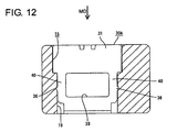
- FIGS. 11 and 12 show the construction of a board fixing portion 30A.
- no repetitive description is given on the same or similar construction as the first embodiment by identifying it by the same reference numerals.
- a main portion 31 of the board fixing portion 30A is formed with at least one (preferably substantially rectangular) bored portion 39.
- This bored portion 39 is formed in a middle or intermediate portion 34 of the main portion 31, whereby at least one pair of arm portions 40 supported at both ends are formed at the opposite sides of the middle portion 34.
- Each arm portion 40 has a retaining portion 36 on the outer side edge thereof, and is resiliently deformable inward. Accordingly, upon at least partly inserting the board fixing portion 30A in the mounting direction MD into a mount groove 15, the arm portions 40 undergo such inward resilient deformation as to move away from the groove edges of a narrower portion 19 as the retaining portions 36 come substantially into contact with the groove edges.
- the board fixing portion 30A can be inserted without using a jig, thereby making operability even better.
- the retaining portions 36 bite in the groove edges of the narrower portions 19 to retain the board fixing portion 30A in the mount groove 15 as shown in FIG. 12.
- a circuit board connector C shown in this embodiment is comprised of one or more, preferably a plurality of terminal fittings 20, a connector housing 10 (hereinafter, merely housing 10") into which the respective terminal fittings 20 are at least partly mountable, and one or more, preferably at least one pair of board fixing portions 30 mountable into or to the housing 10.
- the housing 10 is fixed or to be fixed to or mounted onto a circuit board K (as a preferred electric or electronic device) by means of the one or more board fixing portions 30 and is connectable with an unillustrated mating housing.
- a side of the housing 10 to be connected with the mating housing (right side in FIG. 18) is referred to as front side, and reference is made to all the figures except FIGS. 16, 19 and 21 concerning vertical direction VD.
- the housing 10 preferably is laterally substantially long as a whole and includes a terminal holding portion 11 in which the one or more terminal fittings 20 can be held and a receptacle 12 projecting forward from or at the peripheral edge or edge portion of the terminal holding portion 11.
- the terminal holding portion 11 is formed with one or more, preferably a plurality of terminal insertion holes 13 into which the terminal fittings 20 are at least partly insertable from an inserting side, preferably substantially from behind.
- the respective terminal insertion holes 13 are arranged substantially side by side along widthwise direction WD at one or more stages, preferably at two (upper and lower) stages. More specifically, twenty two terminal insertion holes 13 are arranged at the lower stage and eighteen terminal insertion holes 13 are arranged at the upper stage.
- terminal insertion holes are arranged at each of the lateral side (left and rights) of the upper stage shown in FIG. 9.
- the terminal insertion holes 13 at the upper stage and those at the lower stage are at positions displaced (offset) along widthwise direction.
- front and rear ends of each terminal insertion hole 13 are formed to be wider than an intermediate portion 13a.
- the rear end of the terminal insertion hole 13 serves as a receiving portion 13b for receiving a front-stop portion of the terminal fitting 20, whereas the front end thereof serves as an escaping portion 13c for the peripheral edge of the terminal insertion hole 13 scraped or cut away as the terminal fitting 20 is inserted.
- the upper and lower surfaces of the rear end of each terminal insertion hole 13 are formed into slanted or converging surfaces 13d for guiding the insertion of the terminal fitting 20.
- the receptacle 12 preferably is substantially in the form of a rectangular tube having an open front end, and the mating housing is fittable thereinto from front.
- a lock portion 14 engageable with a lock arm of the mating housing to hold the two housings connected projects downward (inward) at an intermediate position (preferably at a substantially widthwise middle position) of the lateral (upper) part of the receptacle 12.
- a mount groove 15 into which the board fixing portion 30 is individually at least partly mountable is provided at (preferably each of the opposite) widthwise end(s) of the receptacle 12 (housing 10).
- Each board fixing portion 30 is made of a (preferably metal) plate separate from the housing 10 and formed by applying bending, folding and/or embossing and the like to a (metal) plate material stamped or cut out into a specific (predetermined or predeterminable) shape. As shown in FIGS. 14, 16 and 17, the board fixing portion 30 is comprised of a main portion 31 preferably substantially in the form of a flat plate extending along vertical direction VD (or the mounting direction MD) and a connecting or soldering portion 32 projecting laterally from a bottom end 35 of the main portion 31 substantially along widthwise direction WD.
- the mount groove 15 into which this board fixing portion 30 is at least partly mountable is comprised of a main-portion accommodating portion 16 into which the main portion 31 is at least partly insertable along the mounting direction MD or a direction of its plate surface, and a soldering-portion accommodating portion 17 into which the soldering portion 32 is at least partly insertable along a direction at an angle different from 0° or 180°, preferably substantially normal to a direction of its plate surface (or mounting direction MD).
- the main portion 31 of the board fixing portion 30 has such a converging or narrowing or stepped outer configuration as to have three widths narrowed from an upper portion 33 (large-width portion) to a middle or intermediate portion 34 (middle-width portion) to a bottom portion 35 (small-width portion) in this order, and the soldering portion 32 is formed to have substantially the same width as the bottom portion 35 to which the soldering portion 32 is coupled.
- the main-portion accommodating portion 16 of the mount groove 15 is such that a wider portion 18 having a width substantially equal to or larger than the upper portion 33 of the main portion 31 and a narrower portion 19 having a width substantially equal to or larger than the middle portion 34 of the main portion 31 are substantially vertically coupled, whereas the soldering-portion accommodating portion 17 is formed to have a width substantially equal to or larger than the bottom portion 35 of the main portion 31 and the soldering portion 32.
- One or more, preferably a pair of retaining portions 36 laterally project from (the substantially opposite side edges of) the middle portion 34 of the main portion 31.
- the retaining portions 36 bite into or engage the groove edges of the narrower portion 19 of the main-portion accommodating portion 16 to retain the board fixing portion 30 in the mount groove 15. Since a projecting distance of the soldering portion 32 preferably is set to be substantially equal to the depth of the soldering-portion accommodating portion 17, the projecting end of the soldering portion 32 is substantially in flush with the outer side surface of the housing 10 with the board fixing portion 30 mounted in the mount groove 15.
- each terminal fitting 20 is formed by applying bending, folding and/or embossing and the like to a conductive (metal) plate material stamped or cut out into a specified (predetermined or predeterminable) shape and includes a base portion 121 held in the terminal holding portion 11 and having its part (rear part 121 b) projecting backward from the terminal holding portion 11 bent at an angle different from 0° or 180°, preferably substantially normal or down or towards the circuit board K at a specified (predetermined or predeterminable) position preferably to be substantially L-shaped.
- the width of a front part 121 a of the base portion 121 to be at least partly inserted into the terminal insertion hole 13 is set to be slightly larger than that of the intermediate portion 13a of the terminal insertion hole 13, the base portion 121 is more or less pressed into the terminal insertion hole 13.
- the width of the rear part 121 b of the base portion 121 projecting backward from the terminal holding portion 11 is set to be smaller than those of the front part 121 a and the intermediate portion 13a of the terminal insertion hole 13.
- a connector-side connecting portion 122 projecting substantially forward from the front surface (connecting surface) of the terminal holding portion 11 and preferably at least partly surrounded by the receptacle 12 is provided at a front side of the base portion 21 to be electrically connected with a mating terminal provided in a mating housing.
- the bottom end of the base portion 21 bent to extend substantially backward (or opposite of the connector-side connecting portion 122) serves as a board-side connecting portion 23, which is electrically connectable with a conductor path (not shown) printed on the circuit board K preferably by soldering, welding, press-fitting or the like.
- the thickness of each terminal fitting 20 preferably is constant over the entire length, and/or the width of the base portion 21 is set to be larger than the thickness thereof.
- One or more, preferably a pair of front-stop portions 24 bulging out sideways are provided at the (preferably substantially opposite) lateral edge(s) of the rear end of the front part 121 a of the base portion 121.
- One or more, preferably aA pair of retaining portions 25 slightly projecting sideways and capable of retaining the terminal fitting 20 in the terminal insertion hole 13 preferably by biting into or engaging the edges of the terminal insertion hole 13 are provided at positions on the opposite lateral edges of the front part 121 a of the base portion 121 before or more forward than the front-stop portions 24.
- the board-side connecting portion 123 is formed to be narrower (substantially along a terminal width direction TWD preferably substantially parallel to the width direction WD) than the rear part 121 b of the base portion 121. More specifically, the width of the board-side connecting portion 123 preferably is set to be substantially equal to the thickness of the terminal fitting 20, and the lower surface thereof in FIG. 3 is substantially in flush with the lower surface of the rear part 121b of the base portion 121, whereas the upper surface thereof in FIG. 16 is located lower (substantially along the vertical direction VD) than the upper surface of the rear part 121 b.
- intervals between adjacent board-side connecting portions 123 along widthwise direction WD are sums of the intervals between the rear parts 121 b of the adjacent base portion 121 and a difference between the width of the rear parts 121 b of the base portions 121 and that of the board-side connecting portions 123.
- the connector-side connecting portion 122 is formed to be narrower than the front part 121 a of the base portion 121 although being wider than the board-side connecting portion 123.
- the front part 121a of the base portion 121 is formed to be wider than the connector-side connecting portion 122.
- a boundary portion between the connector-side connecting portion 122 and the base portion 121 is gradually widened toward the base portion 121, and the opposite side surfaces thereof are formed into one or more slanted insertion guiding surfaces 26. The insertion of the terminal fitting 20 into the terminal insertion hole 13 ca be guided by these insertion guiding surfaces 26.
- the terminal insertion holes 13 preferably are in a so-called offset arrangement. Accordingly, with the respective terminal fittings 20 mounted in the housing 10, the terminal fittings 20 at the upper stage and those at the lower stages are arranged at positions offset along widthwise direction WD as shown in FIGS. 15 and 16, i.e. are in a so-called offset arrangement, and/or the rear end positions of the board-side connecting portions 123 of the terminal fittings 20 at the different (upper and lower) stages are located substantially at the same position along forward and backward directions FBD.
- conductive (preferably metal) plate materials obtained by stamping or cutting a metal plate out into a specified (predetermined or predeterminable) shape are bent, folded and/or embossed.
- the width may be smaller than the thickness at the time of stamping or cutting.
- the entire terminal fitting 20 is elongated in widthwise direction TWD by embossing, thereby obtaining planned width and thickness for each part, and then the base portion 121 is bent substantially at a right angle at a specified position to form a bent portion 121c. Since the bending is applied after the thickness is made smaller than the width, bending precision is improved, with the result that the bent portion 121c can be securely formed to have a planned shape.
- the terminal fittings 20 obtained as above are at least partly mounted into the housing 10 from a state shown in FIGS. 20 and 21.
- the terminal fitting 20 is at least partly inserted into the terminal insertion hole 13 from the front end of the connector-side connecting portion 122 and the base portion 121 enters the intermediate portion 13a of the terminal insertion hole 13 when the terminal fitting 20 reaches a specified (predetermined or predeterminable) depth.
- the base portion 121 is more or less pressed into the intermediate portion 13a of the terminal insertion hole 13 because the width of the front part 121 thereof is larger than that of the intermediate portion 13a, thereby increasing insertion resistance.
- the retaining portions 25 bite in or engage the edges of the terminal insertion hole 13 and the one or more front-stop portions 24 at least partly enter the receiving portion 13b.
- the front end surfaces of the front-stop portions 24 come substantially into contact with the rear end surface of the receiving portion 13b as shown in FIGS. 5 and 6, whereby any further insertion of the terminal fitting 20 can be prevented.
- the retaining portions 25 bite in or engage the edges of the terminal insertion hole 13 to retain the terminal fitting 20 in the terminal insertion hole 13. It should be noted that only the terminal fitting 20 to be arranged at the lower stage is shown in FIG. 20.
- both board fixing portions 30 are mounted into the mount grooves 15 of the housing 10 and then the housing 10 is placed on the circuit board K to fix the board fixing portions 30 to the circuit board K. It does not matter even if the terminal fittings 20 are mounted after the board fixing portions 30 are mounted.
- molten solder is attached to (preferably the peripheral edges of) the soldering portions 32 of the board fixing portions 30 and the board fixing portions 30 are fixed to the circuit board K by solidifying the molten solder.
- the respective terminal fittings 20 are successively soldered or connected.
- the board-side connecting portions 123 of the respective terminal fittings 20 are laid on the corresponding conductor paths on the circuit board K, and preferably the molten solder is attached to the peripheral edges of the board-side connecting portions 123.
- the board-side connecting portions 123 are fixed to the circuit board K while being electrically connected with the conductor paths.
- the circuit board connector C is small and the terminal fittings 20 are in the so-called offset arrangement to make the circuit board connector C smaller along forward and backward directions FBD, intervals between the respective terminal fittings 20 along widthwise direction WD are narrower.
- the board-side connecting portions 123 are formed to be narrower than the rear parts 121 b of the base portions 121, intervals between adjacent board-side connecting portions 123 are wider than those between the rear parts 121b of the base portions 121. As a result, the board-side connecting portions 123 can be easily soldered to the conductor paths. It does not matter even if the board fixing portions 30 are fixed to the circuit board K after the terminal fittings 20 are soldered. Even in such a case, the soldering operation can be successively carried out.
- the mating housing is at least partly fitted into the receptacle 12. Then, mating terminals are electrically connected with the connector-side connecting portions 122.
- the board-side connecting portions 123 of the terminal fittings 20 are formed to the narrower (or have a smaller width along the terminal width direction TWD) than the base portions 121.
- the circuit board connector C suitable for the miniaturization can be provided.
- the terminal fittings 20 are allowed to have a suitable strength even if the width of the connector-side connecting portions 122 are so reduced as to conform to mating terminals as a result of the miniaturization of the connector. Furthermore, the terminal fittings 20 at the upper and those at the lower stages are displaced along widthwise direction WD, i.e. in the so-called offset arrangement, and/or the rear end positions of the connector-side connecting portions 123 of the terminal fittings 20 at the upper and lower stages are located substantially at the same position along forward and backward directions FBD. Therefore, the circuit board connector C can be made smaller along forward and backward directions FBD.
- each terminal fitting 20 is provided with a base portion 121 to be at least partly inserted and preferably held in a housing 10 and a board-side connecting portion 123 provided at the bottom or distal end of the base portion 121 and electrically connectable to a circuit board K preferably by soldering, welding, press-fitting or the like.
- One or more, preferably a plurality of terminal fittings 20 are mounted substantially side by side along widthwise direction WD in the housing 10.
- Each board-side connecting portion 123 is formed to be narrower than the base portion 121. Accordingly, even if intervals between adjacent terminal fittings 20 along widthwise direction WD are narrow, sufficient intervals can be given between the board-side connecting portions 123.
Description
- The present invention relates to a connector which is to be connected or mounted on an electric or electronic device such as a circuit board (so-called circuit board connector).
- One example of a circuit board connector is e.g. known from Japanese Unexamined Patent Publication No.
H05-326049 housing 2 accommodating terminal fittings 1 to acircuit board 3,board fixing portions 4 bulging sideways are integrally formed at the bottom ends of the opposite side surfaces of thehousing 2, andscrews 6 inserted through screw insertion holes formed in thecircuit board 3 are driven intoscrew holes 5 formed in theboard fixing portions 4. - In the above fixing construction, since the
screws 6 bite in the edges of thescrew holes 5, theboard fixing portions 4 need to have a certain size or larger in order to maintain strength, which leads to a tendency to enlarge the entire circuit board connector. - One further example of a circuit board connector is known from
Japanese Unexamined Patent Publication No. H06-325826 - Upon a demand to miniaturize the circuit board connector, it may be necessary to narrow intervals between the terminal fittings along widthwise direction. Since intervals between the board-side connecting portions are also narrowed in such a case, this may make it difficult to individually solder the respective board-side connecting portions to the circuit board.
-
US-A-6 089 883 discloses an electric connector assembly comprising a pair of plug and receptacle board-to-board connectors. Each connector has an insulative housing with a plurality of contacts wherein each contact has substantially a cantilever type spring arm with a maximum deflection apex thereof. Mated plug and receptacle connectors pass the maximum deflection apexes of the contacts with each other to provide positive locking thereof. Each connector further includes a grounding plate longitudinally extending along the housing wherein coupling means are formed respectively on the grounding plate of each connector for combining such pair of grounding plates together. A pair of mounting devices is disposed adjacent two opposite ends of the housing of each connector and mechanically and electrically engaged with the respective distal ends of the corresponding grounding plate in the same connector. -
EP-A-0 789 422 discloses an anti-wicking system for electrical connectors. The anti-wicking system is provided in an electrical connector adapted for mounting on a printed circuit board having solderable circuit traces thereon. The connector includes a housing having a plurality of terminal-receiving passages. A plurality of terminals are inserted into the passages, with solder tail portions of the terminals projecting from the housing for solder connection to the circuit traces on the printed circuit board. The housing has at least one projecting portion adjacent the terminals to provide extra housing material which can be heat staked about the terminals to prevent solder wicking therealong. -
US-A-5 362 256 discloses a connector which is capable of arranging a large number of contacts in an insulator with high density. The connector includes a plurality of leaf contacts and an insulator for holding the contacts. The contact comprises a fixed portion fixed to the insulator, an elastic spring portion integrally connected to one end of the fixed portion, and a contact portion integrally connected to one end of the elastic spring portion and being offset from a surface of the fixed portion and the elastic spring portion. - The present invention was developed in view of the above problem and an object thereof is to miniaturize a connector for an electric or electronic device such as a circuit board.
- This object is solved according to the invention by the features of claim 1. Preferred embodiments of the invention are subject of the dependent claims
- According to the invention, there is provided a connector for mounting to an electric device, particularly being circuit board connector comprising:
- a connector housing, and
- at least one fixing portion for fixing the connector housing to a an electric device,
- wherein the fixing portion comprises a metal plate separate from the connector housing and can be fixed to the electric device by soldering or welding (in particular ultrasonic welding) while being mounted in the connector housing wherein a solder inflow space for permitting at least partial inflow of solder during the soldering is defined between the fixing portion and the connector housing.
- According to a preferred embodiment of the invention, there is provided a circuit board connector, comprising:
- a connector housing, and
- a board fixing portion for fixing the connector housing to a circuit board,
- Since the board fixing portion made of a metal plate is mounted into the connector housing and fixed to the circuit board by soldering, the board fixing portion can be made smaller as compared to a prior art one for fixing a connector housing by means of screw(s). Thus, the entire circuit board connector can be miniaturized.
- Even if an excessive amount of molten solder is used to fix the board fixing portion, the molten solder at least partly flows or can flow into the solder inflow space. This can prevent the molten solder from flowing onto the circuit board.
- Preferably, a plurality of (board) fixing portions are coupled substantially side by side to a carrier via coupling portions, and the board fixing portion is at least partly mounted into the connector housing after being cut off from the carrier at the coupling portion, and
- a soldering portion to be soldered to the circuit board preferably is provided at an end of the (board) fixing portion different from an end thereof where the coupling portion is provided.
- Since the soldering portion is provided at the end of the (board) fixing portion different from the one where the coupling portion is provided, even if burrs are formed upon cutting the coupling portion, these burrs can be prevented from adversely affecting the soldering.
- Most preferably, the connector housing is formed with at least one mount groove into which the (board) fixing portion is at least partly insertable, and
the (board) fixing portion comprises at least one retaining portion for retaining the (board) fixing portion in the mount groove particularly by biting into or engaging a groove edge of the mount groove, and preferably at least one arm portion resiliently deformable to bring the retaining portion away from the groove edge of the mount groove. - Since the retaining portion is brought away from the groove edge of the mount groove through the resilient deformation of the arm portion upon inserting the board fixing portion into the mount groove, a force required to insert the board fixing portion can be reduced. This can lead to an improved mounting operability of the board fixing portion.
- These and other objects, features and advantages of the present invention will become more apparent upon reading of the following detailed description of preferred embodiments and accompanying drawings. It should be understood that even though embodiments are separately described, single features thereof may be combined to additional embodiments.
- FIG. 1 is a front view of a circuit board connector according to a first embodiment of the invention,
- FIG. 2 is a rear view of the circuit board connector,
- FIG. 3 is a section along X-X of FIG. 1,
- FIG. 4 is a plan view of the circuit board connector,
- FIG. 5 is a side view of the circuit board connector,
- FIG. 6 is a section along Y-Y of FIGS. 1 and 4,
- FIG. 7 is a section along Z-Z of FIG. 4,
- FIG. 8 is a side view showing a state where board fixing portions are coupled to a carrier,
- FIG. 9 is a section along Y-Y of FIGS. 1 and 4 showing a state before the board fixing portions are inserted into mount grooves,
- FIG. 10 is a section along Z-Z of FIG. 4 showing the state before the board fixing portions are inserted into the mount grooves,
- FIG. 11 is a section along Y-Y of FIGS. 1 and 4 showing a state before a board fixing portion according to a second embodiment of the invention is inserted into a mount groove,
- FIG. 12 is a section along Y-Y of FIGS. 1 and 4 showing a state where the board fixing portion is mounted,
- FIG. 13 is a perspective view of a prior art circuit board connector,
- FIG. 14 is a front view of a circuit board connector which is background art for this invention ,
- FIG. 15 is a rear view of the background art circuit board connector,
- FIG. 16 is a plan view of the background art circuit board connector,
- FIG. 17 is a side view of the background art circuit board connector,
- FIG. 18 is a section along X-X of FIG. 14,
- FIG. 19 is an enlarged section along Y-Y of FIG. 18,
- FIG. 20 is a section along X-X of FIG. 14 showing a state before the terminal fittings are at least partly inserted, and
- FIG. 21 is an enlarged section along Y-Y of FIG. 20 showing the state before the terminal fittings are at least partly inserted.
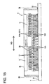
- A first preferred embodiment of the present invention is described with reference to FIGS. 1 to 10. As shown in FIGS. 1 to 5, a circuit board connector shown in this embodiment is comprised of one or more, preferably a plurality of
terminal fittings 20, a connector housing 10 (hereinafter, merelyhousing 10") into which the respective one or moreterminal fittings 20 are at least partly mountable, and one or more, preferably a pair ofboard fixing portions 30 mountable into or onto thehousing 10. Thehousing 10 is to be fixed to a circuit board K (as a preferred electric or electronic device) by means of theboard fixing portions 30 and is connectable with an unillustrated mating housing. In the following description, a side of thehousing 10 to be connected with the mating housing (right side in FIG. 3) is referred to as front side, and reference is made to all the figures except FIG. 4 concerning vertical direction. - As shown in FIGS. 1 to 3, the
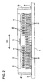
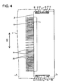
housing 10 preferably is substantially laterally long as a whole and includes aterminal holding portion 11 in which theterminal fittings 20 can be held and preferably areceptacle 12 projecting forward from or at the peripheral edge or edge portion of theterminal holding portion 11. Theterminal holding portion 11 is formed with one or more, preferably a plurality of terminal insertion holes 13 into which theterminal fittings 20 are at least partly insertable from an inserting side, preferably substantially from behind. The respective terminal insertion holes 13 are arranged substantially side by side along widthwise direction WD at one or more stages, preferably at two (upper and lower) stages. More specifically, twenty two terminal insertion holes 13 are arranged at the lower or first stage and eighteen terminal insertion holes 13 are arranged at the upper or second stage. Particularly, nine terminal insertion holes are arranged at each of the left and rights of the upper stage shown in FIG. 1. The terminal insertion holes 13 at the upper stage and those at the lower stage are at positions displaced (offset) along widthwise direction WD. - The
receptacle 12 preferably is substantially in the form of a rectangular tube having an open front end, and the mating housing is at least partly fittable thereinto from a mating side or substantially from front. At least onelock portion 14 engageable with at least one respective lock arm of the mating housing to hold the two housings connected projects downward (inward) at an intermediate position (preferably at a substantially widthwise middle position) of the upper part of thereceptacle 12. Amount groove 15 into which theboard fixing portion 30 is individually mountable is provided at each of the opposite widthwise ends of the receptacle 12 (housing 10). The structure of the mountinggrooves 15 is described in detail later together with theboard fixing portions 30. - A portion of each
terminal fitting 20 projecting backward from theterminal holding portion 11 is bent at an angle different from 0° or 180°, preferably substantially normal or down at a specified (predetermined or predeterminable) position, and the distal or bottom end of this bent or bent-down portion preferably is bent again to extend substantially backward or substantially parallel to a connector-side connecting portion 21. A portion of eachterminal fitting 20 projecting forward from the front surface (connecting surface) of theterminal holding portion 11 and preferably at least partly surrounded by thereceptacle 12 serves as the connector-side connecting portion 21 electrically connectable with a mating terminal arranged in the mating housing. On the other hand, the rear end of the terminal fitting 20 serves as a board-side connecting portion 22 to be electrically connected with the electric or electronic device, preferably with a conductor path (not shown) printed on the circuit board K e.g. by soldering, welding, ultrasonic welding, press-fitting, etc. With theterminal fittings 20 mounted in thehousing 10, theterminal fittings 20 at the upper or second stage are offset from those at the lower or first stage along widthwise direction WD and/or the board-side connecting portions 22 of theterminal fittings 20 at both (upper and lower) stages are located substantially at the same position with respect to forward and backward directions FBD (or a direction at an angle different from 0° or 180°, preferably substantially normal to the widthwise direction WD) as shown in FIGS. 2 to 4. - Next, the
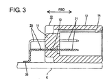
board fixing portions 30 and themount grooves 15 are described in detail. Eachboard fixing portion 30 preferably is made of a (preferably metal) plate separate from thehousing 10 and formed by applying bending, folding and/or embossing and the like to a (metal) plate material stamped or cut out into a specific (predetermined or predeterminable) shape as shown in FIGS. 4 to 7. Theboard fixing portion 30 is comprised of amain portion 31 substantially in the form of a flat plate extending or to be arranged (in use) substantially along vertical direction VD (or a direction at an angle different from 0° or 180°, preferably substantially normal to the widthwise direction WD and/or the forward and backward directions FBD) and a connecting orsoldering portion 32 projecting laterally from a bottom orlateral end 35 of themain portion 31 to be arranged substantially along widthwise direction WD, and preferably is substantially L-shaped as a whole when viewed from front or behind (see FIG. 7). On the other hand, themount groove 15 into which thisboard fixing portion 30 is mountable is comprised of a main-portion accommodating portion 16 into which themain portion 31 is at least partly insertable along a direction of its plate surface, and a connecting- or soldering-portion accommodating portion 17 into which the connecting orsoldering portion 32 is at least partly insertable substantially along a direction normal (or substantially along the forward and backward directions FBD) to a direction of its plate surface (or substantially normal to the vertical direction VD). - As shown in FIG. 6, the
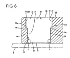
main portion 31 of theboard fixing portion 30 has such a converging or stepped outer configuration as to have two or more, preferably three widths narrowed from an upper portion 33 (large-width portion) to a middle portion 34 (middle-width portion) to a bottom portion 35 (small-width portion) in this order, and thesoldering portion 32 preferably is formed to have substantially the same width as thebottom portion 35 to which thesoldering portion 32 is coupled. On the other hand, the main-portion accommodating portion 16 of themount groove 15 is such that awider portion 18 having a width substantially equal to or larger than theupper portion 33 of themain portion 31 and anarrower portion 19 having a width substantially equal to or larger than themiddle portion 34 of themain portion 31 are vertically coupled or arranged close to each other, whereas the soldering-portion accommodating portion 17 is formed to have a width substantially equal to or larger than thebottom portion 35 of themain portion 31 and thesoldering portion 32. - When the
board fixing portion 30 is at least partly inserted into themount groove 15, a step or narrowedportion 33a at the bottom end of theupper portion 33 of themain portion 31 comes substantially into contact with a step or narrowedportion 18a at the bottom end of thewider portion 18 of the main-portion accommodating portion 16, whereby the bottom surface of theboard fixing portion 30 preferably is so positioned as to be substantially in flush with the bottom surface of thehousing 10. With theboard fixing portion 30 at least partly mounted in themount groove 15, thebottom portion 35 of themain portion 31 is spaced from thenarrower portion 19 of the main-portion accommodating portion 16 by specified (predetermined or predeterminable) clearances, which serve as solder inflow spaces S that are laterally exposed to the outside and permits the at least partial flow or entrance of the solder (as a preferred connecting means) during a connecting or soldering operation. It should be noted that one ormore notches 17a are formed at the bottom or distal ends of the groove edges of the soldering-portion accommodating portion 17 in order to facilitate the at least partial inflow of the solder (see FIG. 5). One or more, preferably a pair of retainingportions 36 laterally project from the opposite side edges preferably of themiddle portion 34 of themain portion 31. As theboard fixing portion 30 is mounted into themount groove 15, the retainingportions 36 bite into or engage the groove edges of thenarrower portion 19 of the main-portion accommodating portion 16 to retain theboard fixing portion 30 in themount groove 15. Since a projecting distance of thesoldering portion 32 is set to be substantially equal to the depth of the soldering-portion accommodating portion 17, the projecting end of thesoldering portion 32 preferably is substantially in flush with the outer side surface of thehousing 10 with theboard fixing portion 30 at least partly mounted in themount groove 15. - In a production process, a plurality of
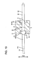
board fixing portions 30 preferably are (temporarily) coupled substantially side by side to acarrier 37 extending in the widthwise direction of the board fixing portions 30 (see FIG. 8). More specifically, the respectiveboard fixing portions 30 are coupled to thecarrier 37 viacoupling portions 38 formed at the upper ends (ends opposite (different) from the soldering portions 32) of themain portions 31, and thecoupling portions 38 are cut to separate theboard fixing portions 30 from thecarrier 37 upon or after or before mounting theboard fixing portions 30 into thehousing 10. - Next, the functions of this embodiment constructed as above are described. After chained board fixing portions as shown in FIG. 8 are formed by stamping or cutting a (preferably metal) blank out and bending, folding and/or embossing the
soldering portions 32, therespective coupling portions 38 are cut at their intermediate positions (substantially same positions as the upper end positions of the main portions 31) to separate the respectiveboard fixing portions 30 from thecarrier 37. On the other hand, the respectiveterminal fittings 20 are at least partly inserted into the terminal insertion holes 13 of thehousing 10 preferably substantially from behind to be mounted. - Subsequently, the
board fixing portions 30 are at least partly mounted into thehousing 10. When theboard fixing portions 30 are at least partly inserted into themount grooves 15 in a mounting direction MD (preferably from above or substantially along the vertical direction VD) substantially along the direction of the plate surfaces of themain portions 31 from a state shown in FIGS. 9 and 10, themain portions 31 and thesoldering portions 32 at least partly enter the main-portion accommodating portions 16 and the soldering-portion accommodating portions 17, respectively. During this mounting operation, the upper ends (ends toward the coupling portions 38) of themain portions 31 preferably are pushed by an unillustrated jig. Upon entering thenarrower portions 19, themiddle portions 34 move substantially in the mounting direction MD or downward while the retainingportions 36 bite into or engage the groove edges of thenarrower portions 19. After theupper portions 33 at least partly enter thewider portions 18, thesteps 33 of theupper portions 33 come substantially into contact with thesteps 18a of thewider portions 18 as shown in FIGS. 6 and 7, whereby any further insertion of theboard fixing portions 30 in the mounting direction MD can be prevented. In this state, the bottom end surfaces of themain portions 31 and thesoldering portions 32 preferably are so positioned as to be substantially in flush with the bottom end surface of thehousing 10. Further, in this state, the retainingportions 36 bite in or engage the groove edges of thenarrower portions 19, thereby preventing theboard fixing portions 30 from coming (upward) out of themount grooves 15. It does not matter even if theterminal fittings 20 are mounted after theboard fixing portions 30 are mounted. - Next, the
housing 10 having one or more, preferably bothboard fixing portions 30 at least partly mounted therein is or is to be fixed to the circuit board K (as the preferred electric or electronic device). After thehousing 10 is at least partly placed substantially on the circuit board K and thesoldering portions 32 of bothboard fixing portions 30 are disposed at or near positions of the circuit board K planned to fix thesoldering portions 32, molten solder is attached to the peripheral edges of thesoldering portions 32. At this time, even if an amount of the molten solder is excessive, the molten solder at least partly flows into the solder inflow spaces S defined between thebottom portions 35 of themain portions 31 and thenarrower portions 19 of the main-portion accommodating portions 16. This can prevent the molten solder from flowing onto the circuit board K. Theboard fixing portions 30 are fixed to the circuit board K by solidifying the attached solder. - Subsequently, the respective
terminal fittings 20 are successively soldered. The board-side connecting portions 22 of the respectiveterminal fittings 20 are laid substantially on or near the corresponding conductor paths on the circuit board K, and the molten solder is attached to the peripheral edges of the board-side connecting portions 22. By solidifying the attached molten solder, The board-side connecting portions 22 are fixed to the circuit board K while being electrically connected with the conductor paths. It does not matter even if theboard fixing portions 30 are fixed to the circuit board K after theterminal fittings 20 are soldered. Even in such a case, the soldering operation can be successively carried out. - As described above, according to this embodiment, the
board fixing portions 30 made of a metal plate are mounted into thehousing 10 and are fixed to the circuit board K by soldering. Thus, as compared to the prior art circuit board connector whose housing is fixed by means of screws, theboard fixing portions 30 can be made smaller, with the result that the entire circuit board connector can be miniaturized. Further, since the operation of fixing theboard fixing portions 30 and the operation of soldering theterminal fittings 20 can be successively carried out in addition to being unnecessary to tighten up screws as with the prior art, operability is better. - Further, since the solder inflow spaces S are at least partly defined between the
board fixing portions 30 and thehousing 10, the redundant solder at least partly flows or can at least partly flow into the solder inflow spaces S even if an amount of the molten solder is excessive upon soldering theboard fixing portions 30. Therefore, the solder can be advantageously prevented from flowing onto the circuit board K. - Since the
soldering portion 32 is provided at the end or side of theboard fixing portion 30 different from the end where thecoupling portion 38 is provided, even if burrs are formed as thecoupling portion 38 is cut, they can be prevented from adversely affecting the soldering. - In this embodiment, the
terminal fittings 20 at the upper stage and those at the lower stage are offset along widthwise direction WD and/or the board-side connecting portions 22 of theterminal fittings 20 at the upper and lower stages are located substantially at the same position with respect to forward and backward directions FBD. Accordingly, as compared to circuit board connectors that tend to be long along forward and backward directions by arranging board-side connecting portions of terminal fittings at upper and lower stages in an offset manner along forward and backward directions, the entire circuit board connector can be made smaller along forward and backward directions. - Accordingly, to miniaturize a circuit board connector, a
housing 10 is formed with one ormore mount grooves 15 into whichboard fixing portions 30 made of a metal plate are at least partly mountable. Eachboard fixing portion 30 is comprised of amain portion 31 and a soldering portion 32 (as a preferred connecting portion) projecting laterally from abottom portion 35 of themain portion 31. Theboard fixing portions 30 can be fixed to a circuit board K by placing thehousing 10 on the circuit board K and preferably by soldering thesoldering portions 32 of theboard fixing portions 30 with theboard fixing portions 30 at least partly mounted in themount grooves 15. - Next, a second preferred embodiment of the present invention is described with reference to FIGS. 11 and 12. The second embodiment shows the construction of a
board fixing portion 30A. In the second embodiment, no repetitive description is given on the same or similar construction as the first embodiment by identifying it by the same reference numerals. - As shown in FIG. 11, a
main portion 31 of theboard fixing portion 30A is formed with at least one (preferably substantially rectangular)bored portion 39. Thisbored portion 39 is formed in a middle orintermediate portion 34 of themain portion 31, whereby at least one pair ofarm portions 40 supported at both ends are formed at the opposite sides of themiddle portion 34. Eacharm portion 40 has a retainingportion 36 on the outer side edge thereof, and is resiliently deformable inward. Accordingly, upon at least partly inserting theboard fixing portion 30A in the mounting direction MD into amount groove 15, thearm portions 40 undergo such inward resilient deformation as to move away from the groove edges of anarrower portion 19 as the retainingportions 36 come substantially into contact with the groove edges. Since biting movements of the retainingportions 36 are alleviated, a force required to insert theboard fixing portion 30A is smaller as compared to the first embodiment. Thus, theboard fixing portion 30A can be inserted without using a jig, thereby making operability even better. When theboard fixing portion 30A is inserted up to a proper depth, the retainingportions 36 bite in the groove edges of thenarrower portions 19 to retain theboard fixing portion 30A in themount groove 15 as shown in FIG. 12. - The present invention is not limited to the above described and illustrated embodiments. For example, the following embodiment is also embraced by the technical scope of the present invention as defined by the claims. Beside the following embodiment, various changes can be made without departing from the scope and spirit of the present invention as defined by the claims.
- (1) The shape of the board fixing portion can be arbitrarily changed. For example, the board fixing portion of the first embodiment may be formed with such a bored portion as not to form arm portions.
- (2) In the foregoing embodiments, the housing may be formed with positioning projections and the circuit board may be formed with positioning recesses, so that the positioning projections are at least partly fittable into the positioning recesses to locate the soldering portions of both board fixing portions at positions of the circuit board planned to fix the board fixing portions to the circuit board and to position the board-side connecting portions of the respective terminal fittings on the corresponding conductor paths.
- (3) Although the solder inflow spaces are at least partly defined by forming the bottom portion of the main portion of the board fixing portion to be narrower than the middle portion in the foregoing embodiments, they may be defined, for example, by forming the middle and bottom portions of the main portion to have the same width and forming the bottom end of the narrower portion of the mount groove to be partly wider.
- (4) Although the coupling portion is provided at the upper end of the main portion opposite from the soldering portion in the foregoing embodiments, it may be, for example, provided at a lateral end of the main portion. It does not matter even if the coupling portion is provided at the bottom end of the main portion.
- (5) The arm portions of the second embodiment may be supported only at one end according to the present invention.
- (6) Although the terminal fittings are connected to the circuit board by soldering in the foregoing embodiments, the present invention is also applicable to connectors in which board-side connecting portions are connected by being pressed into a circuit board, i.e. so-called press-fit terminals are used. Further, the shape of the terminal fittings is not limited to a substantially L-shape and the present invention is also applicable to connectors in which straight terminal fittings are used. The present invention is also applicable to cases where male terminal fittings are mounted in a mating housing and terminal fittings are formed to have female connector-side connecting portions.
- A further embodiment which does not form part of the present invention is described with reference to FIGS. 14 to 21 as background art useful understanding the invention. A circuit board connector C shown in this embodiment is comprised of one or more, preferably a plurality of
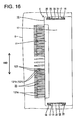
terminal fittings 20, a connector housing 10 (hereinafter, merelyhousing 10") into which the respectiveterminal fittings 20 are at least partly mountable, and one or more, preferably at least one pair ofboard fixing portions 30 mountable into or to thehousing 10. Thehousing 10 is fixed or to be fixed to or mounted onto a circuit board K (as a preferred electric or electronic device) by means of the one or moreboard fixing portions 30 and is connectable with an unillustrated mating housing. In the following description, a side of thehousing 10 to be connected with the mating housing (right side in FIG. 18) is referred to as front side, and reference is made to all the figures except FIGS. 16, 19 and 21 concerning vertical direction VD. - As shown in FIGS. 14 and 18, the
housing 10 preferably is laterally substantially long as a whole and includes aterminal holding portion 11 in which the one or moreterminal fittings 20 can be held and areceptacle 12 projecting forward from or at the peripheral edge or edge portion of theterminal holding portion 11. Theterminal holding portion 11 is formed with one or more, preferably a plurality of terminal insertion holes 13 into which theterminal fittings 20 are at least partly insertable from an inserting side, preferably substantially from behind. The respective terminal insertion holes 13 are arranged substantially side by side along widthwise direction WD at one or more stages, preferably at two (upper and lower) stages. More specifically, twenty two terminal insertion holes 13 are arranged at the lower stage and eighteen terminal insertion holes 13 are arranged at the upper stage. Particularly, nine terminal insertion holes are arranged at each of the lateral side (left and rights) of the upper stage shown in FIG. 9. The terminal insertion holes 13 at the upper stage and those at the lower stage are at positions displaced (offset) along widthwise direction. As shown in FIG. 6, front and rear ends of eachterminal insertion hole 13 are formed to be wider than anintermediate portion 13a. The rear end of theterminal insertion hole 13 serves as a receivingportion 13b for receiving a front-stop portion of the terminal fitting 20, whereas the front end thereof serves as an escapingportion 13c for the peripheral edge of theterminal insertion hole 13 scraped or cut away as the terminal fitting 20 is inserted. Further as shown in FIG. 5, the upper and lower surfaces of the rear end of eachterminal insertion hole 13 are formed into slanted or convergingsurfaces 13d for guiding the insertion of theterminal fitting 20. - The
receptacle 12 preferably is substantially in the form of a rectangular tube having an open front end, and the mating housing is fittable thereinto from front. Alock portion 14 engageable with a lock arm of the mating housing to hold the two housings connected projects downward (inward) at an intermediate position (preferably at a substantially widthwise middle position) of the lateral (upper) part of thereceptacle 12. Amount groove 15 into which theboard fixing portion 30 is individually at least partly mountable is provided at (preferably each of the opposite) widthwise end(s) of the receptacle 12 (housing 10). - Each
board fixing portion 30 is made of a (preferably metal) plate separate from thehousing 10 and formed by applying bending, folding and/or embossing and the like to a (metal) plate material stamped or cut out into a specific (predetermined or predeterminable) shape. As shown in FIGS. 14, 16 and 17, theboard fixing portion 30 is comprised of amain portion 31 preferably substantially in the form of a flat plate extending along vertical direction VD (or the mounting direction MD) and a connecting orsoldering portion 32 projecting laterally from abottom end 35 of themain portion 31 substantially along widthwise direction WD. On the other hand, themount groove 15 into which thisboard fixing portion 30 is at least partly mountable is comprised of a main-portion accommodating portion 16 into which themain portion 31 is at least partly insertable along the mounting direction MD or a direction of its plate surface, and a soldering-portion accommodating portion 17 into which thesoldering portion 32 is at least partly insertable along a direction at an angle different from 0° or 180°, preferably substantially normal to a direction of its plate surface (or mounting direction MD). - The
main portion 31 of theboard fixing portion 30 has such a converging or narrowing or stepped outer configuration as to have three widths narrowed from an upper portion 33 (large-width portion) to a middle or intermediate portion 34 (middle-width portion) to a bottom portion 35 (small-width portion) in this order, and thesoldering portion 32 is formed to have substantially the same width as thebottom portion 35 to which thesoldering portion 32 is coupled. On the other hand, the main-portion accommodating portion 16 of themount groove 15 is such that awider portion 18 having a width substantially equal to or larger than theupper portion 33 of themain portion 31 and anarrower portion 19 having a width substantially equal to or larger than themiddle portion 34 of themain portion 31 are substantially vertically coupled, whereas the soldering-portion accommodating portion 17 is formed to have a width substantially equal to or larger than thebottom portion 35 of themain portion 31 and thesoldering portion 32. - One or more, preferably a pair of retaining
portions 36 laterally project from (the substantially opposite side edges of) themiddle portion 34 of themain portion 31. As theboard fixing portion 30 is at least partly mounted in the mounting direction MD into themount groove 15, the retainingportions 36 bite into or engage the groove edges of thenarrower portion 19 of the main-portion accommodating portion 16 to retain theboard fixing portion 30 in themount groove 15. Since a projecting distance of thesoldering portion 32 preferably is set to be substantially equal to the depth of the soldering-portion accommodating portion 17, the projecting end of thesoldering portion 32 is substantially in flush with the outer side surface of thehousing 10 with theboard fixing portion 30 mounted in themount groove 15. - As shown in FIG. 18, each terminal fitting 20 is formed by applying bending, folding and/or embossing and the like to a conductive (metal) plate material stamped or cut out into a specified (predetermined or predeterminable) shape and includes a
base portion 121 held in theterminal holding portion 11 and having its part (rear part 121 b) projecting backward from theterminal holding portion 11 bent at an angle different from 0° or 180°, preferably substantially normal or down or towards the circuit board K at a specified (predetermined or predeterminable) position preferably to be substantially L-shaped. Since the width of a front part 121 a of thebase portion 121 to be at least partly inserted into theterminal insertion hole 13 is set to be slightly larger than that of theintermediate portion 13a of theterminal insertion hole 13, thebase portion 121 is more or less pressed into theterminal insertion hole 13. On the other hand, the width of therear part 121 b of thebase portion 121 projecting backward from theterminal holding portion 11 is set to be smaller than those of the front part 121 a and theintermediate portion 13a of theterminal insertion hole 13. - A connector-
side connecting portion 122 projecting substantially forward from the front surface (connecting surface) of theterminal holding portion 11 and preferably at least partly surrounded by thereceptacle 12 is provided at a front side of thebase portion 21 to be electrically connected with a mating terminal provided in a mating housing. On the other hand, the bottom end of thebase portion 21 bent to extend substantially backward (or opposite of the connector-side connecting portion 122) serves as a board-side connecting portion 23, which is electrically connectable with a conductor path (not shown) printed on the circuit board K preferably by soldering, welding, press-fitting or the like. The thickness of eachterminal fitting 20 preferably is constant over the entire length, and/or the width of thebase portion 21 is set to be larger than the thickness thereof. - One or more, preferably a pair of front-
stop portions 24 bulging out sideways are provided at the (preferably substantially opposite) lateral edge(s) of the rear end of the front part 121 a of thebase portion 121. When the terminal fitting 20 is inserted to a substantially proper depth into theterminal insertion hole 13, the front end surfaces of the front-stop portions 24 come substantially into contact with the rear end surface of the receivingportion 13b, whereby the terminal fitting 20 can be so stopped as not to move any further forward from a substantially proper insertion position. One or more, preferably aA pair of retainingportions 25 slightly projecting sideways and capable of retaining the terminal fitting 20 in theterminal insertion hole 13 preferably by biting into or engaging the edges of theterminal insertion hole 13 are provided at positions on the opposite lateral edges of the front part 121 a of thebase portion 121 before or more forward than the front-stop portions 24. - As shown in FIGS. 15, 16 and 19, the board-
side connecting portion 123 is formed to be narrower (substantially along a terminal width direction TWD preferably substantially parallel to the width direction WD) than therear part 121 b of thebase portion 121. More specifically, the width of the board-side connecting portion 123 preferably is set to be substantially equal to the thickness of the terminal fitting 20, and the lower surface thereof in FIG. 3 is substantially in flush with the lower surface of therear part 121b of thebase portion 121, whereas the upper surface thereof in FIG. 16 is located lower (substantially along the vertical direction VD) than the upper surface of therear part 121 b. Accordingly, intervals between adjacent board-side connecting portions 123 along widthwise direction WD are sums of the intervals between therear parts 121 b of theadjacent base portion 121 and a difference between the width of therear parts 121 b of thebase portions 121 and that of the board-side connecting portions 123. - On the other hand, the connector-
side connecting portion 122 is formed to be narrower than the front part 121 a of thebase portion 121 although being wider than the board-side connecting portion 123. In other words, the front part 121a of thebase portion 121 is formed to be wider than the connector-side connecting portion 122. A boundary portion between the connector-side connecting portion 122 and thebase portion 121 is gradually widened toward thebase portion 121, and the opposite side surfaces thereof are formed into one or more slanted insertion guiding surfaces 26. The insertion of the terminal fitting 20 into theterminal insertion hole 13 ca be guided by these insertion guiding surfaces 26. - As described above, the terminal insertion holes 13 preferably are in a so-called offset arrangement. Accordingly, with the respective
terminal fittings 20 mounted in thehousing 10, theterminal fittings 20 at the upper stage and those at the lower stages are arranged at positions offset along widthwise direction WD as shown in FIGS. 15 and 16, i.e. are in a so-called offset arrangement, and/or the rear end positions of the board-side connecting portions 123 of theterminal fittings 20 at the different (upper and lower) stages are located substantially at the same position along forward and backward directions FBD. - Next, the functions of this embodiment constructed as above are described. Upon producing the
terminal fittings 20, conductive (preferably metal) plate materials obtained by stamping or cutting a metal plate out into a specified (predetermined or predeterminable) shape are bent, folded and/or embossed. Here, depending on the metal plate used, the width may be smaller than the thickness at the time of stamping or cutting. In such a case, the entire terminal fitting 20 is elongated in widthwise direction TWD by embossing, thereby obtaining planned width and thickness for each part, and then thebase portion 121 is bent substantially at a right angle at a specified position to form abent portion 121c. Since the bending is applied after the thickness is made smaller than the width, bending precision is improved, with the result that thebent portion 121c can be securely formed to have a planned shape. - The
terminal fittings 20 obtained as above are at least partly mounted into thehousing 10 from a state shown in FIGS. 20 and 21. Theterminal fitting 20 is at least partly inserted into theterminal insertion hole 13 from the front end of the connector-side connecting portion 122 and thebase portion 121 enters theintermediate portion 13a of theterminal insertion hole 13 when the terminal fitting 20 reaches a specified (predetermined or predeterminable) depth. At this time, thebase portion 121 is more or less pressed into theintermediate portion 13a of theterminal insertion hole 13 because the width of thefront part 121 thereof is larger than that of theintermediate portion 13a, thereby increasing insertion resistance. However, since the insertion resistance gradually increases by the insertion guiding surfaces 26 gradually biting into or engaging the edges of theterminal insertion hole 13, the insertion can be smoothly carried out. In this process, the retainingportions 25 bite in or engage the edges of theterminal insertion hole 13 and the one or more front-stop portions 24 at least partly enter the receivingportion 13b. When the terminal fitting 20 reaches the substantially proper depth, the front end surfaces of the front-stop portions 24 come substantially into contact with the rear end surface of the receivingportion 13b as shown in FIGS. 5 and 6, whereby any further insertion of the terminal fitting 20 can be prevented. In this state, the retainingportions 25 bite in or engage the edges of theterminal insertion hole 13 to retain the terminal fitting 20 in theterminal insertion hole 13. It should be noted that only the terminal fitting 20 to be arranged at the lower stage is shown in FIG. 20. - After the insertion of all the
terminal fittings 20 is completed, bothboard fixing portions 30 are mounted into themount grooves 15 of thehousing 10 and then thehousing 10 is placed on the circuit board K to fix theboard fixing portions 30 to the circuit board K. It does not matter even if theterminal fittings 20 are mounted after theboard fixing portions 30 are mounted. Preferabla, molten solder is attached to (preferably the peripheral edges of) thesoldering portions 32 of theboard fixing portions 30 and theboard fixing portions 30 are fixed to the circuit board K by solidifying the molten solder. - Subsequently, the respective
terminal fittings 20 are successively soldered or connected. The board-side connecting portions 123 of the respectiveterminal fittings 20 are laid on the corresponding conductor paths on the circuit board K, and preferably the molten solder is attached to the peripheral edges of the board-side connecting portions 123. By solidifying the attached molten solder, The board-side connecting portions 123 are fixed to the circuit board K while being electrically connected with the conductor paths. At this time, since the circuit board connector C is small and theterminal fittings 20 are in the so-called offset arrangement to make the circuit board connector C smaller along forward and backward directions FBD, intervals between the respectiveterminal fittings 20 along widthwise direction WD are narrower. However, since the board-side connecting portions 123 are formed to be narrower than therear parts 121 b of thebase portions 121, intervals between adjacent board-side connecting portions 123 are wider than those between therear parts 121b of thebase portions 121. As a result, the board-side connecting portions 123 can be easily soldered to the conductor paths. It does not matter even if theboard fixing portions 30 are fixed to the circuit board K after theterminal fittings 20 are soldered. Even in such a case, the soldering operation can be successively carried out. - After the circuit board connector C is mounted on the circuit board K as described above, the mating housing is at least partly fitted into the
receptacle 12. Then, mating terminals are electrically connected with the connector-side connecting portions 122. - As described above, according to this embodiment, the board-
side connecting portions 123 of theterminal fittings 20 are formed to the narrower (or have a smaller width along the terminal width direction TWD) than thebase portions 121. Thus, even if intervals along widthwise direction WD between the respectiveterminal fittings 20 arranged substantially side by side are made smaller due to the miniaturization of the circuit board connector C and the so-called offset arrangement of theterminal fittings 20, sufficient intervals are given between adjacent board-side connecting portions 123, with the result that the board-side connecting portions 123 can be easily connected to the circuit board K. Therefore, the circuit board connector C suitable for the miniaturization can be provided. - Further, since the
base portions 121 are formed to be wider than the connector-side connecting portions 122, theterminal fittings 20 are allowed to have a suitable strength even if the width of the connector-side connecting portions 122 are so reduced as to conform to mating terminals as a result of the miniaturization of the connector. Furthermore, theterminal fittings 20 at the upper and those at the lower stages are displaced along widthwise direction WD, i.e. in the so-called offset arrangement, and/or the rear end positions of the connector-side connecting portions 123 of theterminal fittings 20 at the upper and lower stages are located substantially at the same position along forward and backward directions FBD. Therefore, the circuit board connector C can be made smaller along forward and backward directions FBD. - Accordingly, to provide a circuit board connector suitable for the miniaturization, each terminal fitting 20 is provided with a
base portion 121 to be at least partly inserted and preferably held in ahousing 10 and a board-side connecting portion 123 provided at the bottom or distal end of thebase portion 121 and electrically connectable to a circuit board K preferably by soldering, welding, press-fitting or the like. One or more, preferably a plurality ofterminal fittings 20 are mounted substantially side by side along widthwise direction WD in thehousing 10. Each board-side connecting portion 123 is formed to be narrower than thebase portion 121. Accordingly, even if intervals between adjacentterminal fittings 20 along widthwise direction WD are narrow, sufficient intervals can be given between the board-side connecting portions 123. -
- 10
- housing (connector housing)
- 15
- mount groove
- 30, 30A
- board fixing portion
- 32
- 32 soldering portion
- 35
- 35 bottom portion (end different from an end where a coupling portion is provided)
- 36
- retaining portion
- 37
- carrier
- 38
- coupling portion
- 40
- arm portion
- K
- circuit board
- S
- solder inflow space
- 121
- base portion
- 122
- connector-side connecting portion
- 123
- 123 board-side connecting portion
- C
- circuit board connector
Claims (4)
- A connector for mounting to an electric device (K), particularly being circuit board connector, comprising:a connector housing (10), and
at least one fixing portion (30; 30A) for fixing the connector housing (10) to a an electric device (K),wherein the fixing portion (30; 30A) comprises a metal plate separate from the connector housing (10) and can be fixed to the electric device (K) by soldering or welding while being mounted in the connector housing (10)characterized in that a solder inflow space (S) for permitting the at least partial inflow of solder during the soldering is defined between the fixing portion (30; 30A) and the connector housing (10). - A connector according to claim 1, wherein a plurality of fixing portions (30; 30A) are coupled substantially side by side to a carrier (37) via coupling portions (38), and the fixing portion (30; 30A) is at least partly mounted into the connector housing (10) after being cut off from the carrier (37) at the coupling portion (38).
- A connector according to claim 2, wherein a soldering portion to be soldered to the circuit board is provided at an end of the board fixing portion different from an end thereof where the coupling portion is provided.
- A connector according to one or more of the preceding claims, wherein:the connector housing (10) is formed with at least one mount groove (15) into which the fixing portion (30; 30A) is at least partly insertable, andthe fixing portion (30; 30A) comprises at least one retaining portion (36) for retaining the fixing portion (30; 30A) in the mount groove (15) particularly by biting into a groove edge of the mount groove (15), and preferably an arm portion (40) resiliently deformable to bring the retaining portion (36) away from the groove edge of the mount groove (15).
Applications Claiming Priority (4)
| Application Number | Priority Date | Filing Date | Title |
|---|---|---|---|
| JP2003404638A JP2005166492A (en) | 2003-12-03 | 2003-12-03 | Connector for base board |
| JP2003404638 | 2003-12-03 | ||
| JP2003404637 | 2003-12-03 | ||
| JP2003404637A JP4103788B2 (en) | 2003-12-03 | 2003-12-03 | Board connector |
Publications (3)
| Publication Number | Publication Date |
|---|---|
| EP1538706A2 EP1538706A2 (en) | 2005-06-08 |
| EP1538706A3 EP1538706A3 (en) | 2005-08-03 |
| EP1538706B1 true EP1538706B1 (en) | 2007-10-03 |
Family
ID=34467846
Family Applications (1)
| Application Number | Title | Priority Date | Filing Date |
|---|---|---|---|
| EP04028607A Expired - Fee Related EP1538706B1 (en) | 2003-12-03 | 2004-12-02 | A connector fixing bracket |
Country Status (5)
| Country | Link |
|---|---|
| US (1) | US7134910B2 (en) |
| EP (1) | EP1538706B1 (en) |
| KR (1) | KR100679501B1 (en) |
| CN (1) | CN1332480C (en) |
| DE (1) | DE602004009268T2 (en) |
Families Citing this family (13)
| Publication number | Priority date | Publication date | Assignee | Title |
|---|---|---|---|---|
| JP4560727B2 (en) * | 2005-05-20 | 2010-10-13 | 住友電装株式会社 | Board connector |
| JP4262708B2 (en) * | 2005-09-26 | 2009-05-13 | 住友電装株式会社 | Board connector |
| JP2007188697A (en) * | 2006-01-12 | 2007-07-26 | Tyco Electronics Amp Kk | Fastening fixture, surface mounting component equipped with same, and mounting structure using fastening fixture |
| JP2008059856A (en) * | 2006-08-30 | 2008-03-13 | Sumitomo Wiring Syst Ltd | Board connector |
| JP5012072B2 (en) * | 2007-02-14 | 2012-08-29 | 住友電装株式会社 | Board connector |
| KR100866085B1 (en) * | 2007-03-14 | 2008-10-30 | 한국단자공업 주식회사 | Connector |
| JP2009129778A (en) * | 2007-11-26 | 2009-06-11 | Sumitomo Wiring Syst Ltd | Connector for base plate and electric connection box |
| JP5105194B2 (en) * | 2008-11-04 | 2012-12-19 | 住友電装株式会社 | Board connector |
| JP5449073B2 (en) | 2010-07-27 | 2014-03-19 | 矢崎総業株式会社 | Fixing bracket for components mounted on circuit board |
| JP5581983B2 (en) | 2010-11-11 | 2014-09-03 | 住友電装株式会社 | Board connector |
| CN109314330B (en) * | 2016-06-06 | 2020-11-20 | 日本端子株式会社 | Surface mounting type connector |
| FR3076095B1 (en) * | 2017-12-22 | 2021-01-01 | Valeo Siemens Eautomotive France Sas | BOX ELEMENT FOR ELECTRICAL EQUIPMENT |
| CN110600913A (en) * | 2019-09-06 | 2019-12-20 | 昆山杰顺通精密组件有限公司 | Socket directly connected with printed circuit board |
Family Cites Families (16)
| Publication number | Priority date | Publication date | Assignee | Title |
|---|---|---|---|---|
| US4678250A (en) * | 1985-01-08 | 1987-07-07 | Methode Electronics, Inc. | Multi-pin electrical header |
| US5186633A (en) * | 1991-09-03 | 1993-02-16 | Amp Incorporated | Surface mount electrical connector with interleaved solder tails |
| US5362256A (en) * | 1991-12-24 | 1994-11-08 | Nec Corporation | Connector |
| JP2752024B2 (en) | 1992-03-25 | 1998-05-18 | 矢崎総業株式会社 | Printed circuit board connector |
| US5297966A (en) * | 1992-08-10 | 1994-03-29 | The Whitaker Corporation | Mounting bracket for an electrical connector |
| JP2522147B2 (en) | 1993-05-12 | 1996-08-07 | 日本電気株式会社 | connector |
| SG77096A1 (en) | 1996-02-06 | 2000-12-19 | Molex Inc | Anti-wicking system for electrical connectors |
| CN1162852A (en) * | 1996-02-06 | 1997-10-22 | 莫列斯公司 | Anti-wicking system for electrical connectors |
| CN2313311Y (en) * | 1996-12-30 | 1999-04-07 | 鸿海精密工业股份有限公司 | Electric connector |
| JP2000113926A (en) * | 1998-10-01 | 2000-04-21 | Hirose Electric Co Ltd | Surface mount connector |
| KR20000016098U (en) * | 1999-01-25 | 2000-08-25 | 최연학 | contacting structure for reinforce pin of SMD type connector |
| JP3330559B2 (en) * | 1999-03-15 | 2002-09-30 | 日本圧着端子製造株式会社 | Printed wiring board connector |
| JP3324995B2 (en) * | 1999-04-07 | 2002-09-17 | タイコエレクトロニクスアンプ株式会社 | Electrical connector |
| US6305976B1 (en) * | 2000-04-07 | 2001-10-23 | Amp (Japan), Ltd. | Electrical connector with planar mounting members |
| JP4537732B2 (en) * | 2004-03-04 | 2010-09-08 | 住友電装株式会社 | Board connector |
| JP4013914B2 (en) * | 2004-04-12 | 2007-11-28 | 住友電装株式会社 | Board connector |
-
2004
- 2004-12-01 US US11/000,864 patent/US7134910B2/en not_active Expired - Fee Related
- 2004-12-02 DE DE602004009268T patent/DE602004009268T2/en active Active
- 2004-12-02 EP EP04028607A patent/EP1538706B1/en not_active Expired - Fee Related
- 2004-12-03 KR KR1020040101251A patent/KR100679501B1/en not_active IP Right Cessation
- 2004-12-03 CN CNB2004101001667A patent/CN1332480C/en not_active Expired - Fee Related
Also Published As
| Publication number | Publication date |
|---|---|
| EP1538706A2 (en) | 2005-06-08 |
| KR100679501B1 (en) | 2007-02-07 |
| DE602004009268D1 (en) | 2007-11-15 |
| EP1538706A3 (en) | 2005-08-03 |
| KR20050053520A (en) | 2005-06-08 |
| DE602004009268T2 (en) | 2008-07-10 |
| CN1332480C (en) | 2007-08-15 |
| CN1624989A (en) | 2005-06-08 |
| US7134910B2 (en) | 2006-11-14 |
| US20050124228A1 (en) | 2005-06-09 |
Similar Documents
| Publication | Publication Date | Title |
|---|---|---|
| US7374432B2 (en) | Connector | |
| US7179126B2 (en) | Electrical connector with improved terminals | |
| TWI336978B (en) | ||
| JP3041672B2 (en) | Electrical connectors for printed circuit boards | |
| US8454397B2 (en) | Anti-wicking terminal and connector | |
| US7229298B2 (en) | Electrical connector having an improved grounding path | |
| US20040005794A1 (en) | Construction for mounting a terminal, a circuit board connector and method of mounting it | |
| EP1049202B1 (en) | Electrical connector | |
| JP2005129255A (en) | Connector and connector system | |
| US7029334B2 (en) | Multi way connector | |
| EP1538706B1 (en) | A connector fixing bracket | |
| US6135816A (en) | Electrical connector having an improved construction for fixing shield plates to a receptacle connector | |
| TWM631678U (en) | Integrally shielded cable connector | |
| KR101036167B1 (en) | Electric connector | |
| US4708416A (en) | Electrical connecting terminal for a connector | |
| US20070155227A1 (en) | Electrical connector | |
| US7188408B2 (en) | Method of making a straddle mount connector | |
| US7112072B2 (en) | Ground bus for an electrical connector | |
| EP1557908B1 (en) | A connector | |
| US6692273B1 (en) | Straddle mount connector | |
| US20030171032A1 (en) | Shielding connector, a shielding connector system, a terminal fitting and use thereof | |
| JP2000058161A (en) | Connector | |
| US7261597B2 (en) | Electrical connector with low profile | |
| JPH08124638A (en) | Surface mounting-type connector and electric contact therefor | |
| US10756478B2 (en) | Terminal and method of connecting electric wire to terminal |
Legal Events
| Date | Code | Title | Description |
|---|---|---|---|
| PUAI | Public reference made under article 153(3) epc to a published international application that has entered the european phase |
Free format text: ORIGINAL CODE: 0009012 |
|
| 17P | Request for examination filed |
Effective date: 20041209 |
|
| AK | Designated contracting states |
Kind code of ref document: A2 Designated state(s): AT BE BG CH CY CZ DE DK EE ES FI FR GB GR HU IE IS IT LI LT LU MC NL PL PT RO SE SI SK TR |
|
| AX | Request for extension of the european patent |
Extension state: AL BA HR LV MK YU |
|
| PUAL | Search report despatched |
Free format text: ORIGINAL CODE: 0009013 |
|
| AK | Designated contracting states |
Kind code of ref document: A3 Designated state(s): AT BE BG CH CY CZ DE DK EE ES FI FR GB GR HU IE IS IT LI LT LU MC NL PL PT RO SE SI SK TR |
|
| AX | Request for extension of the european patent |
Extension state: AL BA HR LV MK YU |
|
| AKX | Designation fees paid |
Designated state(s): DE FR |
|
| 17Q | First examination report despatched |
Effective date: 20060125 |
|
| GRAP | Despatch of communication of intention to grant a patent |
Free format text: ORIGINAL CODE: EPIDOSNIGR1 |
|
| GRAS | Grant fee paid |
Free format text: ORIGINAL CODE: EPIDOSNIGR3 |
|
| GRAA | (expected) grant |
Free format text: ORIGINAL CODE: 0009210 |
|
| AK | Designated contracting states |
Kind code of ref document: B1 Designated state(s): DE FR |
|
| REF | Corresponds to: |
Ref document number: 602004009268 Country of ref document: DE Date of ref document: 20071115 Kind code of ref document: P |
|
| ET | Fr: translation filed | ||
| PLBE | No opposition filed within time limit |
Free format text: ORIGINAL CODE: 0009261 |
|
| STAA | Information on the status of an ep patent application or granted ep patent |
Free format text: STATUS: NO OPPOSITION FILED WITHIN TIME LIMIT |
|
| 26N | No opposition filed |
Effective date: 20080704 |
|
| PGFP | Annual fee paid to national office [announced via postgrant information from national office to epo] |
Ref country code: DE Payment date: 20141125 Year of fee payment: 11 |
|
| PGFP | Annual fee paid to national office [announced via postgrant information from national office to epo] |
Ref country code: FR Payment date: 20141208 Year of fee payment: 11 |
|
| REG | Reference to a national code |
Ref country code: DE Ref legal event code: R119 Ref document number: 602004009268 Country of ref document: DE |
|
| REG | Reference to a national code |
Ref country code: FR Ref legal event code: ST Effective date: 20160831 |
|
| PG25 | Lapsed in a contracting state [announced via postgrant information from national office to epo] |
Ref country code: DE Free format text: LAPSE BECAUSE OF NON-PAYMENT OF DUE FEES Effective date: 20160701 |
|
| PG25 | Lapsed in a contracting state [announced via postgrant information from national office to epo] |
Ref country code: FR Free format text: LAPSE BECAUSE OF NON-PAYMENT OF DUE FEES Effective date: 20151231 |