EP1724833A2 - SIP (system-in-package) type package containing analog semiconductor chip and digital semiconductor chip stacked in order, and method for manufacturing the same - Google Patents
SIP (system-in-package) type package containing analog semiconductor chip and digital semiconductor chip stacked in order, and method for manufacturing the same Download PDFInfo
- Publication number
- EP1724833A2 EP1724833A2 EP06010256A EP06010256A EP1724833A2 EP 1724833 A2 EP1724833 A2 EP 1724833A2 EP 06010256 A EP06010256 A EP 06010256A EP 06010256 A EP06010256 A EP 06010256A EP 1724833 A2 EP1724833 A2 EP 1724833A2
- Authority
- EP
- European Patent Office
- Prior art keywords
- semiconductor chip
- analog
- digital
- layer
- set forth
- Prior art date
- Legal status (The legal status is an assumption and is not a legal conclusion. Google has not performed a legal analysis and makes no representation as to the accuracy of the status listed.)
- Withdrawn
Links
Images





Classifications
-
- H—ELECTRICITY
- H10—SEMICONDUCTOR DEVICES; ELECTRIC SOLID-STATE DEVICES NOT OTHERWISE PROVIDED FOR
- H10W—GENERIC PACKAGES, INTERCONNECTIONS, CONNECTORS OR OTHER CONSTRUCTIONAL DETAILS OF DEVICES COVERED BY CLASS H10
- H10W74/00—Encapsulations, e.g. protective coatings
- H10W74/10—Encapsulations, e.g. protective coatings characterised by their shape or disposition
- H10W74/111—Encapsulations, e.g. protective coatings characterised by their shape or disposition the semiconductor body being completely enclosed
- H10W74/114—Encapsulations, e.g. protective coatings characterised by their shape or disposition the semiconductor body being completely enclosed by a substrate and the encapsulations
- H10W74/117—Encapsulations, e.g. protective coatings characterised by their shape or disposition the semiconductor body being completely enclosed by a substrate and the encapsulations the substrate having spherical bumps for external connection
-
- H—ELECTRICITY
- H05—ELECTRIC TECHNIQUES NOT OTHERWISE PROVIDED FOR
- H05K—PRINTED CIRCUITS; CASINGS OR CONSTRUCTIONAL DETAILS OF ELECTRIC APPARATUS; MANUFACTURE OF ASSEMBLAGES OF ELECTRICAL COMPONENTS
- H05K1/00—Printed circuits
- H05K1/02—Details
- H05K1/0201—Thermal arrangements, e.g. for cooling, heating or preventing overheating
- H05K1/0203—Cooling of mounted components
- H05K1/0204—Cooling of mounted components using means for thermal conduction connection in the thickness direction of the substrate
- H05K1/0206—Cooling of mounted components using means for thermal conduction connection in the thickness direction of the substrate by printed thermal vias
-
- H—ELECTRICITY
- H10—SEMICONDUCTOR DEVICES; ELECTRIC SOLID-STATE DEVICES NOT OTHERWISE PROVIDED FOR
- H10W—GENERIC PACKAGES, INTERCONNECTIONS, CONNECTORS OR OTHER CONSTRUCTIONAL DETAILS OF DEVICES COVERED BY CLASS H10
- H10W42/00—Arrangements for protection of devices
- H10W42/20—Arrangements for protection of devices protecting against electromagnetic or particle radiation, e.g. light, X-rays, gamma-rays or electrons
-
- H—ELECTRICITY
- H10—SEMICONDUCTOR DEVICES; ELECTRIC SOLID-STATE DEVICES NOT OTHERWISE PROVIDED FOR
- H10W—GENERIC PACKAGES, INTERCONNECTIONS, CONNECTORS OR OTHER CONSTRUCTIONAL DETAILS OF DEVICES COVERED BY CLASS H10
- H10W44/00—Electrical arrangements for controlling or matching impedance
- H10W44/20—Electrical arrangements for controlling or matching impedance at high-frequency [HF] or radio frequency [RF]
-
- H—ELECTRICITY
- H10—SEMICONDUCTOR DEVICES; ELECTRIC SOLID-STATE DEVICES NOT OTHERWISE PROVIDED FOR
- H10W—GENERIC PACKAGES, INTERCONNECTIONS, CONNECTORS OR OTHER CONSTRUCTIONAL DETAILS OF DEVICES COVERED BY CLASS H10
- H10W72/00—Interconnections or connectors in packages
-
- H—ELECTRICITY
- H10—SEMICONDUCTOR DEVICES; ELECTRIC SOLID-STATE DEVICES NOT OTHERWISE PROVIDED FOR
- H10W—GENERIC PACKAGES, INTERCONNECTIONS, CONNECTORS OR OTHER CONSTRUCTIONAL DETAILS OF DEVICES COVERED BY CLASS H10
- H10W72/00—Interconnections or connectors in packages
- H10W72/50—Bond wires
-
- H—ELECTRICITY
- H10—SEMICONDUCTOR DEVICES; ELECTRIC SOLID-STATE DEVICES NOT OTHERWISE PROVIDED FOR
- H10W—GENERIC PACKAGES, INTERCONNECTIONS, CONNECTORS OR OTHER CONSTRUCTIONAL DETAILS OF DEVICES COVERED BY CLASS H10
- H10W72/00—Interconnections or connectors in packages
- H10W72/851—Dispositions of multiple connectors or interconnections
-
- H—ELECTRICITY
- H10—SEMICONDUCTOR DEVICES; ELECTRIC SOLID-STATE DEVICES NOT OTHERWISE PROVIDED FOR
- H10W—GENERIC PACKAGES, INTERCONNECTIONS, CONNECTORS OR OTHER CONSTRUCTIONAL DETAILS OF DEVICES COVERED BY CLASS H10
- H10W90/00—Package configurations
-
- H—ELECTRICITY
- H10—SEMICONDUCTOR DEVICES; ELECTRIC SOLID-STATE DEVICES NOT OTHERWISE PROVIDED FOR
- H10W—GENERIC PACKAGES, INTERCONNECTIONS, CONNECTORS OR OTHER CONSTRUCTIONAL DETAILS OF DEVICES COVERED BY CLASS H10
- H10W90/00—Package configurations
- H10W90/811—Multiple chips on leadframes
-
- H—ELECTRICITY
- H05—ELECTRIC TECHNIQUES NOT OTHERWISE PROVIDED FOR
- H05K—PRINTED CIRCUITS; CASINGS OR CONSTRUCTIONAL DETAILS OF ELECTRIC APPARATUS; MANUFACTURE OF ASSEMBLAGES OF ELECTRICAL COMPONENTS
- H05K1/00—Printed circuits
- H05K1/02—Details
- H05K1/0296—Conductive pattern lay-out details not covered by sub groups H05K1/02 - H05K1/0295
- H05K1/0298—Multilayer circuits
-
- H—ELECTRICITY
- H05—ELECTRIC TECHNIQUES NOT OTHERWISE PROVIDED FOR
- H05K—PRINTED CIRCUITS; CASINGS OR CONSTRUCTIONAL DETAILS OF ELECTRIC APPARATUS; MANUFACTURE OF ASSEMBLAGES OF ELECTRICAL COMPONENTS
- H05K2201/00—Indexing scheme relating to printed circuits covered by H05K1/00
- H05K2201/09—Shape and layout
- H05K2201/09209—Shape and layout details of conductors
- H05K2201/095—Conductive through-holes or vias
- H05K2201/09563—Metal filled via
-
- H—ELECTRICITY
- H05—ELECTRIC TECHNIQUES NOT OTHERWISE PROVIDED FOR
- H05K—PRINTED CIRCUITS; CASINGS OR CONSTRUCTIONAL DETAILS OF ELECTRIC APPARATUS; MANUFACTURE OF ASSEMBLAGES OF ELECTRICAL COMPONENTS
- H05K3/00—Apparatus or processes for manufacturing printed circuits
- H05K3/40—Forming printed elements for providing electric connections to or between printed circuits
- H05K3/42—Plated through-holes or plated via connections
- H05K3/421—Blind plated via connections
-
- H—ELECTRICITY
- H10—SEMICONDUCTOR DEVICES; ELECTRIC SOLID-STATE DEVICES NOT OTHERWISE PROVIDED FOR
- H10W—GENERIC PACKAGES, INTERCONNECTIONS, CONNECTORS OR OTHER CONSTRUCTIONAL DETAILS OF DEVICES COVERED BY CLASS H10
- H10W70/00—Package substrates; Interposers; Redistribution layers [RDL]
- H10W70/60—Insulating or insulated package substrates; Interposers; Redistribution layers
- H10W70/67—Insulating or insulated package substrates; Interposers; Redistribution layers characterised by their insulating layers or insulating parts
- H10W70/68—Shapes or dispositions thereof
- H10W70/682—Shapes or dispositions thereof comprising holes having chips therein
-
- H—ELECTRICITY
- H10—SEMICONDUCTOR DEVICES; ELECTRIC SOLID-STATE DEVICES NOT OTHERWISE PROVIDED FOR
- H10W—GENERIC PACKAGES, INTERCONNECTIONS, CONNECTORS OR OTHER CONSTRUCTIONAL DETAILS OF DEVICES COVERED BY CLASS H10
- H10W70/00—Package substrates; Interposers; Redistribution layers [RDL]
- H10W70/60—Insulating or insulated package substrates; Interposers; Redistribution layers
- H10W70/67—Insulating or insulated package substrates; Interposers; Redistribution layers characterised by their insulating layers or insulating parts
- H10W70/68—Shapes or dispositions thereof
- H10W70/685—Shapes or dispositions thereof comprising multiple insulating layers
-
- H—ELECTRICITY
- H10—SEMICONDUCTOR DEVICES; ELECTRIC SOLID-STATE DEVICES NOT OTHERWISE PROVIDED FOR
- H10W—GENERIC PACKAGES, INTERCONNECTIONS, CONNECTORS OR OTHER CONSTRUCTIONAL DETAILS OF DEVICES COVERED BY CLASS H10
- H10W72/00—Interconnections or connectors in packages
- H10W72/50—Bond wires
- H10W72/541—Dispositions of bond wires
- H10W72/5449—Dispositions of bond wires not being orthogonal to a side surface of the chip, e.g. fan-out arrangements
-
- H—ELECTRICITY
- H10—SEMICONDUCTOR DEVICES; ELECTRIC SOLID-STATE DEVICES NOT OTHERWISE PROVIDED FOR
- H10W—GENERIC PACKAGES, INTERCONNECTIONS, CONNECTORS OR OTHER CONSTRUCTIONAL DETAILS OF DEVICES COVERED BY CLASS H10
- H10W72/00—Interconnections or connectors in packages
- H10W72/50—Bond wires
- H10W72/541—Dispositions of bond wires
- H10W72/547—Dispositions of multiple bond wires
- H10W72/5473—Dispositions of multiple bond wires multiple bond wires connected to a common bond pad
-
- H—ELECTRICITY
- H10—SEMICONDUCTOR DEVICES; ELECTRIC SOLID-STATE DEVICES NOT OTHERWISE PROVIDED FOR
- H10W—GENERIC PACKAGES, INTERCONNECTIONS, CONNECTORS OR OTHER CONSTRUCTIONAL DETAILS OF DEVICES COVERED BY CLASS H10
- H10W72/00—Interconnections or connectors in packages
- H10W72/851—Dispositions of multiple connectors or interconnections
- H10W72/874—On different surfaces
- H10W72/879—Bump connectors and bond wires
-
- H—ELECTRICITY
- H10—SEMICONDUCTOR DEVICES; ELECTRIC SOLID-STATE DEVICES NOT OTHERWISE PROVIDED FOR
- H10W—GENERIC PACKAGES, INTERCONNECTIONS, CONNECTORS OR OTHER CONSTRUCTIONAL DETAILS OF DEVICES COVERED BY CLASS H10
- H10W72/00—Interconnections or connectors in packages
- H10W72/851—Dispositions of multiple connectors or interconnections
- H10W72/874—On different surfaces
- H10W72/884—Die-attach connectors and bond wires
-
- H—ELECTRICITY
- H10—SEMICONDUCTOR DEVICES; ELECTRIC SOLID-STATE DEVICES NOT OTHERWISE PROVIDED FOR
- H10W—GENERIC PACKAGES, INTERCONNECTIONS, CONNECTORS OR OTHER CONSTRUCTIONAL DETAILS OF DEVICES COVERED BY CLASS H10
- H10W72/00—Interconnections or connectors in packages
- H10W72/90—Bond pads, in general
- H10W72/931—Shapes of bond pads
- H10W72/932—Plan-view shape, i.e. in top view
-
- H—ELECTRICITY
- H10—SEMICONDUCTOR DEVICES; ELECTRIC SOLID-STATE DEVICES NOT OTHERWISE PROVIDED FOR
- H10W—GENERIC PACKAGES, INTERCONNECTIONS, CONNECTORS OR OTHER CONSTRUCTIONAL DETAILS OF DEVICES COVERED BY CLASS H10
- H10W74/00—Encapsulations, e.g. protective coatings
-
- H—ELECTRICITY
- H10—SEMICONDUCTOR DEVICES; ELECTRIC SOLID-STATE DEVICES NOT OTHERWISE PROVIDED FOR
- H10W—GENERIC PACKAGES, INTERCONNECTIONS, CONNECTORS OR OTHER CONSTRUCTIONAL DETAILS OF DEVICES COVERED BY CLASS H10
- H10W90/00—Package configurations
- H10W90/20—Configurations of stacked chips
-
- H—ELECTRICITY
- H10—SEMICONDUCTOR DEVICES; ELECTRIC SOLID-STATE DEVICES NOT OTHERWISE PROVIDED FOR
- H10W—GENERIC PACKAGES, INTERCONNECTIONS, CONNECTORS OR OTHER CONSTRUCTIONAL DETAILS OF DEVICES COVERED BY CLASS H10
- H10W90/00—Package configurations
- H10W90/20—Configurations of stacked chips
- H10W90/291—Configurations of stacked chips characterised by containers, encapsulations, or other housings for the stacked chips
-
- H—ELECTRICITY
- H10—SEMICONDUCTOR DEVICES; ELECTRIC SOLID-STATE DEVICES NOT OTHERWISE PROVIDED FOR
- H10W—GENERIC PACKAGES, INTERCONNECTIONS, CONNECTORS OR OTHER CONSTRUCTIONAL DETAILS OF DEVICES COVERED BY CLASS H10
- H10W90/00—Package configurations
- H10W90/20—Configurations of stacked chips
- H10W90/297—Configurations of stacked chips characterised by the through-semiconductor vias [TSVs] in the stacked chips
-
- H—ELECTRICITY
- H10—SEMICONDUCTOR DEVICES; ELECTRIC SOLID-STATE DEVICES NOT OTHERWISE PROVIDED FOR
- H10W—GENERIC PACKAGES, INTERCONNECTIONS, CONNECTORS OR OTHER CONSTRUCTIONAL DETAILS OF DEVICES COVERED BY CLASS H10
- H10W90/00—Package configurations
- H10W90/701—Package configurations characterised by the relative positions of pads or connectors relative to package parts
- H10W90/721—Package configurations characterised by the relative positions of pads or connectors relative to package parts of bump connectors
- H10W90/724—Package configurations characterised by the relative positions of pads or connectors relative to package parts of bump connectors between a chip and a stacked insulating package substrate, interposer or RDL
-
- H—ELECTRICITY
- H10—SEMICONDUCTOR DEVICES; ELECTRIC SOLID-STATE DEVICES NOT OTHERWISE PROVIDED FOR
- H10W—GENERIC PACKAGES, INTERCONNECTIONS, CONNECTORS OR OTHER CONSTRUCTIONAL DETAILS OF DEVICES COVERED BY CLASS H10
- H10W90/00—Package configurations
- H10W90/701—Package configurations characterised by the relative positions of pads or connectors relative to package parts
- H10W90/731—Package configurations characterised by the relative positions of pads or connectors relative to package parts of die-attach connectors
- H10W90/732—Package configurations characterised by the relative positions of pads or connectors relative to package parts of die-attach connectors between stacked chips
-
- H—ELECTRICITY
- H10—SEMICONDUCTOR DEVICES; ELECTRIC SOLID-STATE DEVICES NOT OTHERWISE PROVIDED FOR
- H10W—GENERIC PACKAGES, INTERCONNECTIONS, CONNECTORS OR OTHER CONSTRUCTIONAL DETAILS OF DEVICES COVERED BY CLASS H10
- H10W90/00—Package configurations
- H10W90/701—Package configurations characterised by the relative positions of pads or connectors relative to package parts
- H10W90/731—Package configurations characterised by the relative positions of pads or connectors relative to package parts of die-attach connectors
- H10W90/734—Package configurations characterised by the relative positions of pads or connectors relative to package parts of die-attach connectors between a chip and a stacked insulating package substrate, interposer or RDL
-
- H—ELECTRICITY
- H10—SEMICONDUCTOR DEVICES; ELECTRIC SOLID-STATE DEVICES NOT OTHERWISE PROVIDED FOR
- H10W—GENERIC PACKAGES, INTERCONNECTIONS, CONNECTORS OR OTHER CONSTRUCTIONAL DETAILS OF DEVICES COVERED BY CLASS H10
- H10W90/00—Package configurations
- H10W90/701—Package configurations characterised by the relative positions of pads or connectors relative to package parts
- H10W90/731—Package configurations characterised by the relative positions of pads or connectors relative to package parts of die-attach connectors
- H10W90/736—Package configurations characterised by the relative positions of pads or connectors relative to package parts of die-attach connectors between a chip and a stacked lead frame, conducting package substrate or heat sink
-
- H—ELECTRICITY
- H10—SEMICONDUCTOR DEVICES; ELECTRIC SOLID-STATE DEVICES NOT OTHERWISE PROVIDED FOR
- H10W—GENERIC PACKAGES, INTERCONNECTIONS, CONNECTORS OR OTHER CONSTRUCTIONAL DETAILS OF DEVICES COVERED BY CLASS H10
- H10W90/00—Package configurations
- H10W90/701—Package configurations characterised by the relative positions of pads or connectors relative to package parts
- H10W90/731—Package configurations characterised by the relative positions of pads or connectors relative to package parts of die-attach connectors
- H10W90/737—Package configurations characterised by the relative positions of pads or connectors relative to package parts of die-attach connectors between a chip and a laterally-adjacent lead frame, conducting package substrate or heat sink
-
- H—ELECTRICITY
- H10—SEMICONDUCTOR DEVICES; ELECTRIC SOLID-STATE DEVICES NOT OTHERWISE PROVIDED FOR
- H10W—GENERIC PACKAGES, INTERCONNECTIONS, CONNECTORS OR OTHER CONSTRUCTIONAL DETAILS OF DEVICES COVERED BY CLASS H10
- H10W90/00—Package configurations
- H10W90/701—Package configurations characterised by the relative positions of pads or connectors relative to package parts
- H10W90/751—Package configurations characterised by the relative positions of pads or connectors relative to package parts of bond wires
- H10W90/754—Package configurations characterised by the relative positions of pads or connectors relative to package parts of bond wires between a chip and a stacked insulating package substrate, interposer or RDL
-
- H—ELECTRICITY
- H10—SEMICONDUCTOR DEVICES; ELECTRIC SOLID-STATE DEVICES NOT OTHERWISE PROVIDED FOR
- H10W—GENERIC PACKAGES, INTERCONNECTIONS, CONNECTORS OR OTHER CONSTRUCTIONAL DETAILS OF DEVICES COVERED BY CLASS H10
- H10W90/00—Package configurations
- H10W90/701—Package configurations characterised by the relative positions of pads or connectors relative to package parts
- H10W90/751—Package configurations characterised by the relative positions of pads or connectors relative to package parts of bond wires
- H10W90/756—Package configurations characterised by the relative positions of pads or connectors relative to package parts of bond wires between a chip and a stacked lead frame, conducting package substrate or heat sink
Definitions
- the present invention relates to a system-in-package type (SIP) package containing an analog semiconductor device and a digital semiconductor device, which may be advantageously used to receive and process a radio frequency (RF) signal in, for example, a global positioning system (GPS), and also relates to a method for manufacturing such a SIP package.
- SIP system-in-package type
- both a radio frequency (RF) signal processing unit and a baseband signal processing unit are required to receive and process a GPS signal.
- the GPS signal is down-converted into an intermediate frequency signal, and then the intermediate frequency signal is demodulated to thereby generate an analog baseband signal.
- the analog baseband signal is converted into a digital baseband signal, and then the digital baseband signal is output to the baseband processing unit.
- the digital baseband signal is further processed to thereby generate a GPS position information signal.
- the RF signal processing unit is formed as an analog semiconductor package, and the baseband signal processing unit is formed as a digital semiconductor package. These semiconductor packages are mounted on a wiring board of the GPS-signal receiver apparatus, and other various units are also mounted on the wiring board.
- the GPS-signal receiver apparatus is a large size and bulky, and is unsuitable for use in a small piece of electronic equipment, such as a mobile phone terminal, a personal digital assistant (PDA) or the like.
- a mobile phone terminal such as a mobile phone terminal, a personal digital assistant (PDA) or the like.
- PDA personal digital assistant
- JP-2004-214249-A discloses a prior art semiconductor package containing two digital semiconductor chips, one of which is arranged above the other semiconductor chip.
- this package may contribute to downsizing of the wiring board of the GPS-signal receiver apparatus.
- JP-2002-033439-A discloses another prior art semiconductor package containing both an analog RF signal processing semiconductor chip and a digital baseband signal processing semiconductor chip, with the former being arranged above the latter. This package may also contribute to downsizing of the wiring board of the GPS-signal receiver apparatus.
- the analog RF signal processing semiconductor chip is susceptible to high frequency noises, especially generated from the digital baseband signal processing semiconductor chip.
- a semiconductor package which includes a wiring board having a ground layer formed therein, an analog semiconductor chip provided on or above the ground layer, and a digital semiconductor chip provided on or above the analog semiconductor chip such that a substrate of the digital semiconductor chip is directed toward the analog semiconductor chip.
- the analog semiconductor chip may be formed as a radio frequency signal processing semiconductor chip, and the digital semiconductor chip may be formed as a baseband signal processing semiconductor chip.
- the ground layer is coextended with respect to the analog semiconductor chip.
- an active layer of the analog semiconductor chip may be directed toward an upside, but an active layer of the digital semiconductor chip is directed toward the upside.
- the analog semiconductor chip and the digital semiconductor chip are connected to a wiring pattern layer, formed on the wiring board, with a plurality of conductive wires.
- an active layer of the analog semiconductor chip may be directed toward a downside, but an active layer of the digital semiconductor chip is directed toward an upside.
- the digital semiconductor chip is mounted on a substrate of the analog semiconductor chip.
- the analog semiconductor chip has a plurality of metal bumps provided on the active layer thereof, and is connected to a wiring pattern layer, formed on the wiring board, with the metal bumps. Further, the digital semiconductor chip are connected to the wiring pattern layer with a plurality of conductive wires.
- the digital semiconductor chip features a wider size than that of the analog semiconductor chip.
- the semiconductor package may further include a spacer unit provided between the analog semiconductor chip and the digital semiconductor chip.
- the semiconductor package may further include an impedance matching circuit provided on the wiring board for the analog semiconductor, and a molded resin enveloper encapsulating the analog and digital semiconductor chips and the impedance matching circuit.
- the semiconductor package may further include a band pass filter provided on the wiring board for the analog semiconductor chip, and a molded resin enveloper encapsulating the analog and digital semiconductor chips and the band pass filter.
- the semiconductor package may further includes a plurality of metal balls securely attached as electrode terminals to respective electrode pads formed on a bottom surface of the wiring board.
- the wiring board may be formed as a multi-layered wiring board including at least a lowermost insulating layer, an intermediate insulating layer, and an uppermost insulating layer.
- the ground layer is formed in the uppermost insulating layer so that the analog semiconductor chip is positioned on the ground layer.
- the ground layer is formed in the intermediate insulating layer just below the uppermost insulating layer so that the analog semiconductor chip is positioned above the ground layer.
- a method for manufacturing a semiconductor package comprising: preparing a wiring board; forming a ground layer in the wiring board; providing an analog semiconductor chip on or above the ground layer; and providing a digital semiconductor chip on or above the analog semiconductor chip such that a substrate of the digital semiconductor chip is directed toward the analog semiconductor chip.
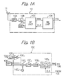
- the GPS-signal receiver apparatus 10 includes a band pass filter unit 10A, an impedance matching circuit unit 10B, an RF signal processing unit 10C, a band pass filter unit 10D and a baseband signal processing unit 10E. Note that these units 10A through 10E are mounted on a suitable wiring board (not shown).
- the band pass filter unit 10A is connected to a GPS antenna 11 at an input terminal thereof for receiving a GPS signal.
- the RF signal processing unit 10C is constituted as an analog semiconductor package containing an analog RF signal processing semiconductor chip
- the baseband signal processing unit 10E is constituted as a digital semiconductor package containing a digital baseband signal processing semiconductor chip.
- the impedance matching circuit unit 10B is symbolically represented by a characteristic impedance Z 0 .
- the GPS antenna 11 receives a GPS-signal having a frequency of 1575.42 MHz, and the GPS signal is transmitted to the band pass filter 10A in which noises are filtered out of the GPS signal, and then the GPS signal is input to the RF signal processing unit 10C through the impedance matching circuit unit 10B.
- the GPS signal is once amplified, and the amplified GPS signal is output to the band pass filter 10D in which the amplified noises are filtered out of the GPS signal.
- the GPS signal is again input to the RF signal processing unit 10C in which the GPS signal (1575.42 MHz) is down-converted into an intermediate frequency signal, having a frequency falling within a range from several MHz to several tens of MHz, and the intermediate frequency signal is demodulated into an analog baseband signal.
- the analog baseband signal is converted into a digital baseband signal BBS in accordance with a clock signal CLK output from the baseband signal processing unit 10E.
- the digital baseband signal BBS is output from the RF signal processing unit 10C to the baseband signal processing unit 10E.
- the baseband signal BBS is suitably processed to thereby generate a GPS position information signal PIS, and the signal PIS is output from the baseband signal processing unit 10E.
- the analog semiconductor package or RF signal processing unit 10C contains an amplifier 10C 1 , a mixer 10C 2 , a local oscillator 10C 3 , a low pass filter 10C 4 , a demodulator 10C 5 , and an output circuit 10C 6 .
- the output circuit 10C 6 has a sample hold circuit, an analog-to-digital converter, a frequency divider and so on, and is operated in accordance with the clock signal CLK output from the baseband signal processing unit 10E.
- the aforesaid amplification of the GPS signal is carried out by the amplifier 10C 1 .
- Both the mixer 10C 2 and the local oscillator 10C 3 serves as a down-converter for converting the GPS signal (1575.42 MHz) into the intermediate frequency signal (several MHz to several tens of MHz).
- the mixer 10C 2 mixes the GPS signal with a local frequency signal, output from the local oscillator 10C 3 , to thereby generate the intermediate frequency signal, which is input to the low pass filter 10C 4 in which noises are filtered out of the intermediate frequency signal.
- the aforesaid demodulation of the intermediate frequency into the analog baseband signal is carried out by the demodulator 10C 5
- the aforesaid conversion of the analog baseband signal into the digital baseband signal is carried out by the output circuit 10C 6 .
- the clock signal CLK which is input from the baseband signal processing unit 10E, is divided by the frequency divider circuit into a clock signal having a lower frequency than that of the clock signal CLK.
- the analog baseband signal is sampled by the sample hold circuit in accordance with the clock signal having the lower frequency, and the sampled signal is converted into the digital baseband signal BBS in accordance with the clock pulses CLK.
- the above-mentioned GPS-signal receiver apparatus is constructed as a large-sized apparatus in that the various units 10A through 10E are mounted on the wiring board, and thus is unsuitable for use in a small piece of electronic equipment, such as a mobile phone terminal, a personal digital assistant (PDA) or the like.
- a small piece of electronic equipment such as a mobile phone terminal, a personal digital assistant (PDA) or the like.
- PDA personal digital assistant
- the GPS-signal receiver apparatus is mounted on a motherboard for the small piece of electronic equipment, a mounting area on the motherboard, which is occupied by the wiring board of the GPS-signal receiver apparatus, is considerably large.
- FIG. 2 a part of a prior art semiconductor package is illustrated in a cross-sectional view, and this prior art semiconductor package is disclosed in, for example, JP-2004-214249-A .
- the semiconductor package includes a multi-layered wiring board 20 having a plurality of insulating layers 20A, 20B, 20C, 20D and 20E, which are stacked in order.
- Each of the insulating layers 20A through 20E has a wiring pattern layer (not shown) formed thereon, and has a plurality of through holes (not shown) formed therein to thereby establish electrical connections between the two adjacent wiring pattern layers.
- the lowermost insulating layer 20A has a ground layer 20A 1 formed on a bottom surface thereof, with the ground layer 20A 1 serving as a heat radiation layer 20A 1 . Also, the lowermost insulating layer 20A has a plurality of electrode pads 20A 2 formed on the bottom surface thereof. Note, in Fig. 2, only one of the el ectrode terminals 22 is representatively illustrated.
- the uppermost insulating layer 20E has a plurality of electrode pads 20E 1 and a plurality of electrode pads 20E 2 , which are formed on a top surface thereof, and each of the electrode pads is connected to the wiring pattern layer formed on the top surface of the uppermost insulating layer 20E.
- the wiring pattern layer formed on the uppermost insulating layer 20E is connected to the electrode pads 20A 2 through the intermediary of the through holes and the wiring pattern layers intervened therebetween.
- the multi-layered wiring board 20 has a rectangular recess 21 which is formed in both the insulating layers 20D and 20E above the ground layer or heat radiation layer 20A 1 .
- a plurality of metal plugs 22 are formed in the insulating layers 20A, 20B and 20C at a bottom of the rectangular recess 21 so as to reach the heat radiation layer 20A 1 .
- a plurality of metal plugs 23 are formed in the insulating layers 20A, 20B, 20C, 20D and 20E so as to reach the heat radiation layer 20A 1 , and are arranged to surround the rectangular recess 21.
- the semiconductor package also includes a digital semiconductor chip 24 which is mounted on and adhered to the bottom of the rectangular recess 21 with an adhesive layer 25, and the digital semiconductor chip 24 is connected to the electrode pads 20E 1 with bonding wires 26 1 .
- the digital semiconductor chip 24 is thermally connected to the heat radiation layer 20A 1 through the metal plugs 22, and thus it is possible to facilitate radiation of heat from the digital semiconductor chip 24.
- the semiconductor package further includes a digital semiconductor chip 27 which is mounted on and secured to a plurality of metal support balls 28 fixed on respective top faces of the metal plugs 23, and the digital semiconductor chip 27 is connected to the electrode pads 20E 2 with bonding wires 26 2 .
- the digital semiconductor chip 27 also is thermally connected to the heat radiation layer 20A 1 through the metal plugs 26, and thus it is possible to facilitate radiation of heat from the digital semiconductor chip 27.
- these chips 24 and 25 are sealed together with the wiring pattern layer, the electrode pads 20E 1 and 20E 2 and the bonding wires 26 1 and 26 2 with a molded resin enveloper 29, only a contour of which is shown by a phantom line in Fig. 2 for simplicity of illustration.
- the semiconductor chip 27 is arranged above the semiconductor chip 24 in the molded resin enveloper 29.
- a mounting area on the motherboard which is occupied by the wiring board of the GPS-signal receiver apparatus, is relatively small.
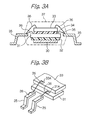
- FIG. 3A is a cross-sectional view of the QFP type semiconductor package
- Fig. 3B is a partial perspective view of Fig. 3A.
- the QFP type semiconductor package includes an island or mount plate 30, a digital baseband signal processing semiconductor chip 31 mounted on and adhered to the mount plate 30 with an adhesive layer 32, an analog RF signal processing semiconductor chip 33 mounted on and adhered to the digital baseband signal processing semiconductor chip 31 with an adhesive layer 34, a plurality of leads 35 connected to the baseband signal processing chip 31 and the RF signal processing semiconductor chip 33 by bonding wires 36, and a molded resin enveloper 37 which seals and encapsulates the mount plate 30, the semiconductor chips 31 and 33, the bonding wires 36, and inner sections of the shaped leads 35.
- a contour of the molded resin enveloper 37 is shown by a phantom line for a simplicity of illustration.
- the digital baseband signal processing semiconductor chip 31 has an electrode pad 31A formed on a top surface thereof, and a bonding wire 36 is connected to the baseband signal processing semiconductor chip 31 at the corresponding electrode pad 31A.
- the analog RF signal processing semiconductor chip 33 has an electrode pad 33A formed on a top surface thereof, and a bonding wire 36 is connected to the RF signal processing semiconductor chip 33 at the corresponding electrode pad 33A.
- a tuning wire 38 is suitably provided as an inductance element at the leads 35 of the baseband signal processing semiconductor chip 31, which are used for transmitting high frequency signals, to thereby improve an impedance characteristic in the leads 35 concerned.
- the RF signal processing semiconductor chip 33 is susceptible to being influenced by high frequency noises, especially generated from the baseband signal processing semiconductor chip 31, because an active layer of the RF signal processing semiconductor chip 33, in which various elements such as transistors, capacitors, resistors, inductors and so on, are formed, is only covered with a part of the molded resin enveloper 37.
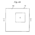
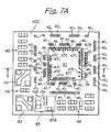
- Figs. 4A through 8A are plan views for explaining the manufacturing method
- Figs. 4B through 8B are cross-sectional views taken along the B-B lines of Figs. 4A through 8A, respectively.
- a multi-layered wiring board 40 which is called a package board or an interposer, is prepared.
- the multi-layered wiring board 40 includes four insulating layers: a lowermost insulating layer 40A, an intermediate insulating layer 40B, an intermediate insulating layer 40C, and an uppermost insulating layer 40D, which are stacked in order, and each of the insulating layers 40A, 40B, 40C and 40D may be composed of a suitable resin material such as epoxy resin.
- each of the lowermost and intermediate insulating layers 40A, 40B and 40C has a wiring pattern layer formed on a top surface thereof, and a plurality of through holes formed therein to thereby establish electrical connections between the two adjacent wiring pattern layers.
- the wiring pattern layers and the through holes may be composed of a suitable metal material such as copper (Cu), and the formation of the wiring pattern layers and the through holes may be carried out by using a photolithography and etching process.
- the lowermost insulating layer 40A has a plurality of electrode pads 40A 1 formed on a bottom surface thereof, and these electrode pads 40A 1 are suitably connected to the wiring pattern layer, formed on the top surface of the lowermost insulating layer 40A, through the intermediary of through holes (not shown) formed therein.
- a recess 41 is formed in the uppermost insulating layer 40D, and a plurality of through holes (not shown) are formed in the uppermost insulating layer 40D by using a photolithography and etching process.
- a copper (Cu) layer 42 is formed on the top surface of the uppermost insulating layer 40D by using a copper plating process, so that the recess 40D 1 is stuffed with copper.
- the thickness of each of the insulating layers 40A, 40B, 40C and 40D is exaggeratedly illustrated, in reality, it is very thin so that the formation of the Cu layer 42 is substantially evenly carried out without the Cu layer 42 sagging at the recess 41.
- the Cu layer 42 (see: Figs. 5A and 5B) is patterned by using a photolithography and etching process, so that a plurality of electrode pads 42 1 and a plurality of electrode pads 42 2 are formed on the top surface of the uppermost insulating layer 40D, and so that a copper (Cu) layer section 42 3 is left as a ground layer at the rectangular recess 41.
- the electrode pads 42 1 are arranged so as to surround the Cu layer section or rectangular ground layer 42 3
- the electrode pads 42 2 are arranged along an outer periphery of the arrangement of the electrode pads 42 1 .
- a wiring pattern layer is further formed on the top surface of the uppermost insulating layer 40D by the aforesaid photolithography and etching process, it is not shown in Figs. 6A and 6B to avoid complexity of illustration.
- the wiring pattern layer formed on the top surface of the uppermost insulating layer 40D is suitably connected to the aforesaid through holes formed therein, to thereby establish electrical connections between the wiring pattern layer concerned and the electrode pads 40A 1 formed on the bottom surface of the lowermost insulating layer 40A.
- electrode pads 42 1 and 42 2 are suitably connected to the wiring pattern layer concerned.
- band pass filter units 43 and 44 are mounted on the uppermost insulating layer 40D so as to be suitably connected to the wiring pattern layer concerned, and each of the band pass filter units 43 and 44 may be formed as a surface acoustic wave (SAW) type chip.
- SAW surface acoustic wave
- the band pass filter units 43 and 44 correspond to the band pass filter units 10A and 10D of the GPS-signal receiver apparatus 10 of Figs. 1A and 1B.
- an impedance matching circuit 45 is constituted by mounting and arranging various passive elements 45A and 45B on the uppermost insulating layer 40D, with the impedance matching circuit 45 being suitably connected to the wiring pattern layer (not shown) on the uppermost insulating layer 40D.
- each of the passive elements 45A is formed as a capacitor chip
- each of the passive elements 45B is formed as an inductor chip.
- the impedance matching circuit 45 corresponds to the impedance matching circuit unit 10B of the GPS-signal receiver apparatus 10 of Figs. 1A and 1B.
- various passive elements are mounted and arranged on the uppermost insulating layer 40D, if necessary, and are suitably connected to the wiring pattern layer (not shown) on the uppermost wiring layer 40D.
- a part of the passive elements 46 may be represented by a resistor chip, and another part of the passive elements may be represented by a capacitor chip.
- a signal-strength conversion circuit is constituted by some of the passive elements 46.
- an analog rectangular semiconductor chip 47 is securely mounted on the rectangular ground layer 42 3 by using a suitable adhesive agent.
- the RF signal processing semiconductor chip 47 includes a substrate 47A, and an active layer 47B formed on the substrate 47A, and the active layer 47B includes various elements, such as transistors, capacitors, resistors and so on formed therein.
- the mounting of the RF signal processing semiconductor chip 47 on the ground layer 42 3 is carried out such that the active layer 47B is directed toward the upside.
- the rectangular RF signal processing semiconductor chip 47 has a plurality of electrode pads 47C which are formed on a surface of the active layer 47B so as to be arranged along the four sides thereof.
- the electrode pads 47C are connected to the electrode pads 42 1 , formed on the uppermost insulating layer 40D, with bonding wires 48 1 by using a wire bonding machine (not shown).
- a spacer member 49 which may be made of a suitable resin material, is securely mounted on the RF signal processing semiconductor chip 47 by using a suitable adhesive agent, and a digital rectangular baseband signal processing semiconductor chip 50 having a larger size than that of the RF signal processing semiconductor chip 47 is securely mounted on the spacer member 49 by using a suitable adhesive agent.
- the spacer member 49 is provided for avoiding an interference between the bonding wires 48 2 and the baseband signal processing semiconductor chip 50.
- the baseband signal processing semiconductor chip 50 includes a substrate 50A, and an active layer 50B formed on the substrate 50A, and the active layer 50B includes various elements, such as transistors, capacitors, resistors and so on formed therein.
- the mounting of the baseband signal processing semiconductor chip 50 on the spacer member 49 is carried out such that the active layer 50B is directed toward the upside.
- the rectangular baseband signal processing semiconductor chip 50 has a plurality of electrode pads 50C which are formed on a surface of the active layer 50B so as to be arranged along the four sides thereof.
- the electrode pads 50C are connected to the electrode pads 42 2 , formed on the uppermost insulating layer 40D, with bonding wires 48 2 by using the wire bonding machine (not shown).
- this SIP type package features a ball grid array (BGA) formed by the metal balls 52.
- BGA ball grid array
- the aforesaid signal-strength conversion circuit which is explained with reference to Fig. 6A, is used to regulate the strength of a baseband signal to be input from the RF signal processing semiconductor chip 47 to the baseband signal processing semiconductor chip 50.
- the SIP type package thus produced can operate in substantially the same manner as the GPS-signal receiver apparatus 10 of Figs. 1A and 1B, this package is considerably downsized in comparison with the GPS-signal receiver apparatus 10 of Figs. 1A and 1B, in that all the elements (43, 44, 45, 46, 47, 50, etc.) are integrated as one package.
- the ground layer 42 3 is coextended with respect to the RF signal processing semiconductor chip 47 so that a ground ability of the ground layer 47 is sufficiently fortified.
- a current flowing through the substrate 47A can be effectively drained out into the ground layer 42 3 , whereby it is possible to stably maintain a high frequency characteristic of the RF signal processing semiconductor chip 47.
- the active layer 47B of the RF signal processing semiconductor chip 47 is covered with the substrate 50A of the baseband signal processing semiconductor chip 50, and an electric potential of the substrate 50A is relatively stable during an operation of the baseband signal processing semiconductor chip 50, so that the substrate 50A serves as an effective electromagnetic shield.
- the RF signal processing semiconductor chip 47 can be effectively protected from high frequency noises.
- the baseband signal processing semiconductor chip 50 During an operation of the baseband signal processing semiconductor chip 50, high frequency noises are generated from the active layer 50B thereof.
- the RF signal processing semiconductor chip 47 may be influenced by the high frequency noises generated from the active layer 50B.
- the RF signal processing semiconductor chip 47 could not be substantially influenced by the high frequency noises generated from the active layer 50B.
- a first group of samples in each of which a baseband signal processing semiconductor chip (50) was stacked on a spacer (49) mounted on an RF signal processing semiconductor chip (47) (see: Fig. 8B), were prepared, and a sensitivity characteristic of the RF signal processing semiconductor chip (47), represented by a signal/noise ratio (SNR), was measured with respect to each of the sample included in the first group.
- a second group of samples in each of which an RF signal processing semiconductor chip (47) was directly stacked on a baseband signal processing semiconductor chip (50), and a sensitivity characteristic of the RF signal processing semiconductor chip (47), represented by a signal/noise ratio (SNR), was measured with respect to each of the samples included in the second group.
- the AUTONOMOUS mode was used, and the input/output (I/0) voltage was 2.9 V.
- the strength of a GPS signal was set in -130 dBm, but it were variable between a maximum value and a minimum value. The measurements ware carried out at the maximum and minimum values of the strength of the GPS signal.
- the results measured on the first group of samples were superior to the results measured on the second group of samples by approximately 3dB.
- the substrate 50A of the baseband signal processing semiconductor chip 50 functions as the effective electromagnetic shield for protecting the RF signal processing semiconductor chip 47.
- the baseband signal processing semiconductor chip 50 has a wider size than that of the RF signal processing semiconductor chip 47, the latter may be wider than the former, if necessary. In this case, if there is no interference between the bonding wires 48 2 and the baseband signal processing semiconductor chip 50, the spacer member 49 could be omitted. Namely, the baseband signal processing semiconductor chip 50 may be directly adhered to the RF signal processing semiconductor chip 47 without using the spacer member 49.
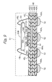
- Fig. 9 which corresponds to Fig. 8A, a modification of the aforesaid embodiment of the SIP type package according to the present invention is shown.
- a flip-chip (FC) type analog RF signal processing semiconductor chip 53 is substituted for the RF signal processing semiconductor chip 47, and includes a substrate 53A, and an active layer 53B formed on the substrate 53A.
- the FC type analog RF signal processing semiconductor chip 53 has a plurality of metal bumps 53C which are securely attached as electrode terminals to a surface of the active layer 53B.
- the ground layer 42 3 is omitted from the uppermost insulating layer 40D, and a ground layer 54 is formed instead in the intermediate insulating layer 40C just below the uppermost insulating layer 40D. Similar to the formation of the ground layer 42 3 , the formation of the ground layer 54 is carried out at the same time when the wiring pattern layer (not shown) is formed on the intermediate insulating layer 40C.
- the wiring pattern layer formed on the uppermost insulating layer 40D has a plurality of electrode pads (not shown) which are arranged so as to have a mirror image relationship with respect to the arrangement of the metal bumps 53C.
- the FC type RF signal processing semiconductor chip 53 is flipped over and mounted on the uppermost insulating layer 40D such that the metal bumps are contacted with and bounded on the respective electrode pads.
- the ground layer 54 is coextended with respect to the FC type RF signal processing semiconductor chip 53 so that a ground ability of the ground layer 54 is sufficiently fortified.
- the substrate 50A of the baseband signal processing semiconductor chip 50 serves as an effective electromagnetic shield.
Landscapes
- Engineering & Computer Science (AREA)
- Microelectronics & Electronic Packaging (AREA)
- Manufacturing & Machinery (AREA)
- Semiconductor Integrated Circuits (AREA)
- Position Fixing By Use Of Radio Waves (AREA)
Abstract
In a semiconductor package, a wiring board (40) having a ground layer (423, 54) is formed therein. An analog semiconductor chip (47, 53) is provided on or above the ground layer, and a digital semiconductor chip (50) is provided on or above the analog semiconductor chip such that a substrate (50A) of the digital semiconductor chip is directed toward the analog semiconductor chip.
Description
- The present invention relates to a system-in-package type (SIP) package containing an analog semiconductor device and a digital semiconductor device, which may be advantageously used to receive and process a radio frequency (RF) signal in, for example, a global positioning system (GPS), and also relates to a method for manufacturing such a SIP package.
- In a GPS-signal receiver apparatus, both a radio frequency (RF) signal processing unit and a baseband signal processing unit are required to receive and process a GPS signal. Namely, in the RF signal processing unit, the GPS signal is down-converted into an intermediate frequency signal, and then the intermediate frequency signal is demodulated to thereby generate an analog baseband signal. The analog baseband signal is converted into a digital baseband signal, and then the digital baseband signal is output to the baseband processing unit. Next, in the baseband signal processing unit, the digital baseband signal is further processed to thereby generate a GPS position information signal.
- The RF signal processing unit is formed as an analog semiconductor package, and the baseband signal processing unit is formed as a digital semiconductor package. These semiconductor packages are mounted on a wiring board of the GPS-signal receiver apparatus, and other various units are also mounted on the wiring board.
- Thus, the GPS-signal receiver apparatus is a large size and bulky, and is unsuitable for use in a small piece of electronic equipment, such as a mobile phone terminal, a personal digital assistant (PDA) or the like.
-
JP-2004-214249-A -
JP-2002-033439-A - It has now been discovered that the above-mentioned prior arts have a problem to be solved as mentioned hereinbelow.
- The above-mentioned prior arts cannot sufficiently contribute to the downsizing of the wiring board of the GPS-signal receiver apparatus, in that various units, such as a band pass filter unit, an impedance matching circuit and so on must be further mounted on the wiring board GPS-signal receiver apparatus.
- Also, in the prior art disclosed in
JP-2002-033439-A - In accordance with a first aspect of the present invention, there is provided a semiconductor package, which includes a wiring board having a ground layer formed therein, an analog semiconductor chip provided on or above the ground layer, and a digital semiconductor chip provided on or above the analog semiconductor chip such that a substrate of the digital semiconductor chip is directed toward the analog semiconductor chip.
- The analog semiconductor chip may be formed as a radio frequency signal processing semiconductor chip, and the digital semiconductor chip may be formed as a baseband signal processing semiconductor chip. Preferably, the ground layer is coextended with respect to the analog semiconductor chip.
- In this semiconductor package, an active layer of the analog semiconductor chip may be directed toward an upside, but an active layer of the digital semiconductor chip is directed toward the upside. In this case, the analog semiconductor chip and the digital semiconductor chip are connected to a wiring pattern layer, formed on the wiring board, with a plurality of conductive wires.
- On the other hand, an active layer of the analog semiconductor chip may be directed toward a downside, but an active layer of the digital semiconductor chip is directed toward an upside. In this case, the digital semiconductor chip is mounted on a substrate of the analog semiconductor chip. Also, the analog semiconductor chip has a plurality of metal bumps provided on the active layer thereof, and is connected to a wiring pattern layer, formed on the wiring board, with the metal bumps. Further, the digital semiconductor chip are connected to the wiring pattern layer with a plurality of conductive wires.
- Preferably, the digital semiconductor chip features a wider size than that of the analog semiconductor chip.
- The semiconductor package may further include a spacer unit provided between the analog semiconductor chip and the digital semiconductor chip.
- The semiconductor package may further include an impedance matching circuit provided on the wiring board for the analog semiconductor, and a molded resin enveloper encapsulating the analog and digital semiconductor chips and the impedance matching circuit.
- The semiconductor package may further include a band pass filter provided on the wiring board for the analog semiconductor chip, and a molded resin enveloper encapsulating the analog and digital semiconductor chips and the band pass filter.
- The semiconductor package may further includes a plurality of metal balls securely attached as electrode terminals to respective electrode pads formed on a bottom surface of the wiring board.
- Preferably, the wiring board may be formed as a multi-layered wiring board including at least a lowermost insulating layer, an intermediate insulating layer, and an uppermost insulating layer.
- In the semiconductor package, when the active layer of the analog semiconductor chip is directed toward the upside, and when the active layer of the digital semiconductor chip is directed toward the upside, the ground layer is formed in the uppermost insulating layer so that the analog semiconductor chip is positioned on the ground layer.
- On the other hand, when the active layer of the analog semiconductor chip is directed toward the downside, and when an active layer of the digital semiconductor chip is directed toward the upside, the ground layer is formed in the intermediate insulating layer just below the uppermost insulating layer so that the analog semiconductor chip is positioned above the ground layer.
- In accordance with a second aspect of the present invention, there is provided a method for manufacturing a semiconductor package comprising: preparing a wiring board; forming a ground layer in the wiring board; providing an analog semiconductor chip on or above the ground layer; and providing a digital semiconductor chip on or above the analog semiconductor chip such that a substrate of the digital semiconductor chip is directed toward the analog semiconductor chip.
- The present invention will be more clearly understood from the description set forth below, with reference to the accompanying drawings, wherein:
- Figure 1A is a block circuit diagram of a prior art GPS-signal receiver apparatus;
- Figure 1B is a block circuit diagram of the RF signal processing unit of Fig. 1A;
- Figure 2 is a partial cross-sectional view of a prior art semiconductor package;
- Figure 3A is a cross-sectional view of another prior art semiconductor package;
- Figure 3B is a partial perspective view of Fig. 3A;
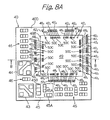
- Figures 4A through 8A are plan views for explaining a method for manufacturing an embodiment of a SIP type package according to the present invention;
- Figures 4B through 8B are cross-sectional views taken along the B-B lines of Figs. 4A through 8A, respectively; and
- Figure 9 is a cross-sectional view showing a modification of the embodiment of the SIP type package of Figs. 8A and 8B.
- Before the description of the preferred embodiments of the present invention, for better understanding of the present invention, a prior art GPS-signal receiver apparatus will be now explained with reference to Figs. 1A and 1B.
- First, referring to Fig. 1A, the GPS-signal receiver apparatus, generally indicated by
reference numeral 10, is illustrated in a block diagram. The GPS-signal receiver apparatus 10 includes a bandpass filter unit 10A, an impedancematching circuit unit 10B, an RFsignal processing unit 10C, a bandpass filter unit 10D and a basebandsignal processing unit 10E. Note that theseunits 10A through 10E are mounted on a suitable wiring board (not shown). The bandpass filter unit 10A is connected to aGPS antenna 11 at an input terminal thereof for receiving a GPS signal. The RFsignal processing unit 10C is constituted as an analog semiconductor package containing an analog RF signal processing semiconductor chip, and the basebandsignal processing unit 10E is constituted as a digital semiconductor package containing a digital baseband signal processing semiconductor chip. Note, in Fig. 1A, the impedancematching circuit unit 10B is symbolically represented by a characteristic impedance Z0. - In operation, the
GPS antenna 11 receives a GPS-signal having a frequency of 1575.42 MHz, and the GPS signal is transmitted to theband pass filter 10A in which noises are filtered out of the GPS signal, and then the GPS signal is input to the RFsignal processing unit 10C through the impedancematching circuit unit 10B. In the RFsignal processing unit 10C, the GPS signal is once amplified, and the amplified GPS signal is output to theband pass filter 10D in which the amplified noises are filtered out of the GPS signal. - Subsequently, the GPS signal is again input to the RF
signal processing unit 10C in which the GPS signal (1575.42 MHz) is down-converted into an intermediate frequency signal, having a frequency falling within a range from several MHz to several tens of MHz, and the intermediate frequency signal is demodulated into an analog baseband signal. Then, the analog baseband signal is converted into a digital baseband signal BBS in accordance with a clock signal CLK output from the basebandsignal processing unit 10E. Next, the digital baseband signal BBS is output from the RFsignal processing unit 10C to the basebandsignal processing unit 10E. - In the digital semiconductor package or baseband
signal processing unit 10E, the baseband signal BBS is suitably processed to thereby generate a GPS position information signal PIS, and the signal PIS is output from the basebandsignal processing unit 10E. - As shown in Fig. 1B, the analog semiconductor package or RF
signal processing unit 10C contains anamplifier 10C1, amixer 10C2, alocal oscillator 10C3, alow pass filter 10C4, ademodulator 10C5, and anoutput circuit 10C6. Note, theoutput circuit 10C6 has a sample hold circuit, an analog-to-digital converter, a frequency divider and so on, and is operated in accordance with the clock signal CLK output from the basebandsignal processing unit 10E. - In the RF
signal processing unit 10C, the aforesaid amplification of the GPS signal is carried out by theamplifier 10C1. Both themixer 10C2 and thelocal oscillator 10C3 serves as a down-converter for converting the GPS signal (1575.42 MHz) into the intermediate frequency signal (several MHz to several tens of MHz). Namely, themixer 10C2 mixes the GPS signal with a local frequency signal, output from thelocal oscillator 10C3, to thereby generate the intermediate frequency signal, which is input to thelow pass filter 10C4 in which noises are filtered out of the intermediate frequency signal. - Then, the aforesaid demodulation of the intermediate frequency into the analog baseband signal is carried out by the
demodulator 10C5, and the aforesaid conversion of the analog baseband signal into the digital baseband signal is carried out by theoutput circuit 10C6. - In particular, the clock signal CLK, which is input from the baseband
signal processing unit 10E, is divided by the frequency divider circuit into a clock signal having a lower frequency than that of the clock signal CLK. The analog baseband signal is sampled by the sample hold circuit in accordance with the clock signal having the lower frequency, and the sampled signal is converted into the digital baseband signal BBS in accordance with the clock pulses CLK. - The above-mentioned GPS-signal receiver apparatus is constructed as a large-sized apparatus in that the
various units 10A through 10E are mounted on the wiring board, and thus is unsuitable for use in a small piece of electronic equipment, such as a mobile phone terminal, a personal digital assistant (PDA) or the like. In particular, when the GPS-signal receiver apparatus is mounted on a motherboard for the small piece of electronic equipment, a mounting area on the motherboard, which is occupied by the wiring board of the GPS-signal receiver apparatus, is considerably large. - Also, in the prior art of Figs. 1A and 1B, when a plurality of GPS-
signal receiver apparatuses 10 are produced, it is necessary to individually adjust theimpedance matching units 10B, resulting in an increase in production cost for the GPS-signal receiver apparatuses 10. - With reference to Fig. 2, a part of a prior art semiconductor package is illustrated in a cross-sectional view, and this prior art semiconductor package is disclosed in, for example,
JP-2004-214249-A - The semiconductor package includes a
multi-layered wiring board 20 having a plurality of insulatinglayers layers 20A through 20E has a wiring pattern layer (not shown) formed thereon, and has a plurality of through holes (not shown) formed therein to thereby establish electrical connections between the two adjacent wiring pattern layers. - In the
multi-layered wiring board 20, the lowermost insulatinglayer 20A has aground layer 20A1 formed on a bottom surface thereof, with theground layer 20A1 serving as aheat radiation layer 20A1. Also, the lowermost insulatinglayer 20A has a plurality ofelectrode pads 20A2 formed on the bottom surface thereof. Note, in Fig. 2, only one of the el ectrodeterminals 22 is representatively illustrated. - On the other hand, the uppermost insulating
layer 20E has a plurality ofelectrode pads 20E1 and a plurality ofelectrode pads 20E2, which are formed on a top surface thereof, and each of the electrode pads is connected to the wiring pattern layer formed on the top surface of the uppermost insulatinglayer 20E. Note, the wiring pattern layer formed on the uppermost insulatinglayer 20E is connected to theelectrode pads 20A2 through the intermediary of the through holes and the wiring pattern layers intervened therebetween. - As shown in Fig. 2, the
multi-layered wiring board 20 has arectangular recess 21 which is formed in both the insulatinglayers heat radiation layer 20A1. A plurality of metal plugs 22 are formed in the insulatinglayers rectangular recess 21 so as to reach theheat radiation layer 20A1. Also, a plurality of metal plugs 23 are formed in the insulatinglayers heat radiation layer 20A1, and are arranged to surround therectangular recess 21. - The semiconductor package also includes a
digital semiconductor chip 24 which is mounted on and adhered to the bottom of therectangular recess 21 with anadhesive layer 25, and thedigital semiconductor chip 24 is connected to theelectrode pads 20E1 with bonding wires 261. Thedigital semiconductor chip 24 is thermally connected to theheat radiation layer 20A1 through the metal plugs 22, and thus it is possible to facilitate radiation of heat from thedigital semiconductor chip 24. - The semiconductor package further includes a
digital semiconductor chip 27 which is mounted on and secured to a plurality ofmetal support balls 28 fixed on respective top faces of the metal plugs 23, and thedigital semiconductor chip 27 is connected to theelectrode pads 20E2 with bonding wires 262. Thedigital semiconductor chip 27 also is thermally connected to theheat radiation layer 20A1 through the metal plugs 26, and thus it is possible to facilitate radiation of heat from thedigital semiconductor chip 27. - After the mounting of the semiconductor chips 24 and 27 is completed, these
chips electrode pads - As shown in Fig. 2, the
semiconductor chip 27 is arranged above thesemiconductor chip 24 in the molded resin enveloper 29. Thus, when the semiconductor package is mounted on a motherboard, a mounting area on the motherboard, which is occupied by the wiring board of the GPS-signal receiver apparatus, is relatively small. - Accordingly, in the prior art of Figs. 1A and 1B, if both the analog RF signal processing semiconductor chip contained in the
RF unit 10C and the digital semiconductor chip contained in the basebandsignal processing unit 10E are constituted as one package, as shown in Fig. 2, this package may contribute to downsizing of the wiring board of the GPS-signal receiver apparatus 10. - With reference to Figs. 3A and 3B, another prior art semiconductor package, which is of quad flat package (QFP) type, is illustrated, and this QFP type semiconductor package is disclosed in, for example,
JP-2002-033439-A - Referring to Fig. 3A, the QFP type semiconductor package includes an island or mount
plate 30, a digital baseband signalprocessing semiconductor chip 31 mounted on and adhered to themount plate 30 with anadhesive layer 32, an analog RF signalprocessing semiconductor chip 33 mounted on and adhered to the digital baseband signalprocessing semiconductor chip 31 with anadhesive layer 34, a plurality ofleads 35 connected to the basebandsignal processing chip 31 and the RF signalprocessing semiconductor chip 33 bybonding wires 36, and a moldedresin enveloper 37 which seals and encapsulates themount plate 30, the semiconductor chips 31 and 33, thebonding wires 36, and inner sections of the shaped leads 35. Note, in Fig. 3A, only a contour of the moldedresin enveloper 37 is shown by a phantom line for a simplicity of illustration. - As representatively shown in Fig. 3B, the digital baseband signal
processing semiconductor chip 31 has anelectrode pad 31A formed on a top surface thereof, and abonding wire 36 is connected to the baseband signalprocessing semiconductor chip 31 at thecorresponding electrode pad 31A. Similarly, the analog RF signalprocessing semiconductor chip 33 has anelectrode pad 33A formed on a top surface thereof, and abonding wire 36 is connected to the RF signalprocessing semiconductor chip 33 at thecorresponding electrode pad 33A. - Also, as shown in Fig. 3A, a
tuning wire 38 is suitably provided as an inductance element at theleads 35 of the baseband signalprocessing semiconductor chip 31, which are used for transmitting high frequency signals, to thereby improve an impedance characteristic in theleads 35 concerned. - In the above-mentioned GPS-
signal receiver apparatus 10 of Fig. 1A and 1B, when the QFP type semiconductor package of Figs. 3A and 3B is substituted for both the RFsignal processing unit 10C and the basebandsignal processing unit 10E, and this substitution may contribute to downsizing of the wiring board of the GPS-signal receiver apparatus 10. However, this downsizing is insufficient in that the bandpass filter unit 10A, the impedancematching circuit unit 10B and the bandpass filter unit 10D must be individually and separately mounted on the wiring board, resulting in bulkiness of the GPS-signal receiver apparatus 10. - In the QFP type semiconductor package of Figs. 3A and 3B, the RF signal
processing semiconductor chip 33 is susceptible to being influenced by high frequency noises, especially generated from the baseband signalprocessing semiconductor chip 31, because an active layer of the RF signalprocessing semiconductor chip 33, in which various elements such as transistors, capacitors, resistors, inductors and so on, are formed, is only covered with a part of the moldedresin enveloper 37. - Next, with reference to Figs. 4A through 8A and Figs. 4B through 8B, a method for manufacturing a first embodiment of a system-in-package (SIP) type package according to the present invention, which is used as a GPS receiver apparatus, will be explained below.
- Note, Figs. 4A through 8A are plan views for explaining the manufacturing method, and Figs. 4B through 8B are cross-sectional views taken along the B-B lines of Figs. 4A through 8A, respectively.
- Referring to Figs. 4A and 4B, a
multi-layered wiring board 40, which is called a package board or an interposer, is prepared. Themulti-layered wiring board 40 includes four insulating layers: a lowermost insulatinglayer 40A, an intermediate insulatinglayer 40B, an intermediate insulatinglayer 40C, and an uppermost insulatinglayer 40D, which are stacked in order, and each of the insulatinglayers - Although not shown in Fig. 4B, each of the lowermost and intermediate insulating
layers - As shown in Fig. 4B, the lowermost insulating
layer 40A has a plurality ofelectrode pads 40A1 formed on a bottom surface thereof, and theseelectrode pads 40A1 are suitably connected to the wiring pattern layer, formed on the top surface of the lowermost insulatinglayer 40A, through the intermediary of through holes (not shown) formed therein. - As shown in Figs. 4A and 4B, a
recess 41 is formed in the uppermost insulatinglayer 40D, and a plurality of through holes (not shown) are formed in the uppermost insulatinglayer 40D by using a photolithography and etching process. - Next, referring to Figs. 5A and 5B, a copper (Cu)
layer 42 is formed on the top surface of the uppermost insulatinglayer 40D by using a copper plating process, so that therecess 40D1 is stuffed with copper. Note, in Fig. 5B, although the thickness of each of the insulatinglayers Cu layer 42 is substantially evenly carried out without theCu layer 42 sagging at therecess 41. - Next, referring to Figs. 6A and 6B, the Cu layer 42 (see: Figs. 5A and 5B) is patterned by using a photolithography and etching process, so that a plurality of
electrode pads 421 and a plurality ofelectrode pads 422 are formed on the top surface of the uppermost insulatinglayer 40D, and so that a copper (Cu)layer section 423 is left as a ground layer at therectangular recess 41. As shown in Fig. 6A, theelectrode pads 421 are arranged so as to surround the Cu layer section orrectangular ground layer 423, and theelectrode pads 422 are arranged along an outer periphery of the arrangement of theelectrode pads 421. - Note, although a wiring pattern layer is further formed on the top surface of the uppermost insulating
layer 40D by the aforesaid photolithography and etching process, it is not shown in Figs. 6A and 6B to avoid complexity of illustration. - Also, note, the wiring pattern layer formed on the top surface of the uppermost insulating
layer 40D is suitably connected to the aforesaid through holes formed therein, to thereby establish electrical connections between the wiring pattern layer concerned and theelectrode pads 40A1 formed on the bottom surface of the lowermost insulatinglayer 40A. - Further, note, the
electrode pads - As shown in Fig. 6A, after the formation of the wiring pattern layer on the uppermost insulating
layer 40D is completed, two bandpass filter units layer 40D so as to be suitably connected to the wiring pattern layer concerned, and each of the bandpass filter units pass filter units pass filter units signal receiver apparatus 10 of Figs. 1A and 1B. - Also, an
impedance matching circuit 45 is constituted by mounting and arranging variouspassive elements layer 40D, with theimpedance matching circuit 45 being suitably connected to the wiring pattern layer (not shown) on the uppermost insulatinglayer 40D. For example, each of thepassive elements 45A is formed as a capacitor chip, and each of thepassive elements 45B is formed as an inductor chip. Note, theimpedance matching circuit 45 corresponds to the impedancematching circuit unit 10B of the GPS-signal receiver apparatus 10 of Figs. 1A and 1B. - Further, various passive elements, representatively indicated by
reference numeral 46, are mounted and arranged on the uppermost insulatinglayer 40D, if necessary, and are suitably connected to the wiring pattern layer (not shown) on theuppermost wiring layer 40D. A part of thepassive elements 46 may be represented by a resistor chip, and another part of the passive elements may be represented by a capacitor chip. For example, a signal-strength conversion circuit is constituted by some of thepassive elements 46. - Next, referring to Figs. 7A and 7B, an analog
rectangular semiconductor chip 47 is securely mounted on therectangular ground layer 423 by using a suitable adhesive agent. - As shown in Fig. 7B, the RF signal
processing semiconductor chip 47 includes asubstrate 47A, and anactive layer 47B formed on thesubstrate 47A, and theactive layer 47B includes various elements, such as transistors, capacitors, resistors and so on formed therein. In short, the mounting of the RF signalprocessing semiconductor chip 47 on theground layer 423 is carried out such that theactive layer 47B is directed toward the upside. - Also, as shown in Fig. 7A, the rectangular RF signal
processing semiconductor chip 47 has a plurality ofelectrode pads 47C which are formed on a surface of theactive layer 47B so as to be arranged along the four sides thereof. - After the mounting of the RF signal
processing semiconductor chip 47 on theground layer 423 is completed, theelectrode pads 47C are connected to theelectrode pads 421, formed on the uppermost insulatinglayer 40D, withbonding wires 481 by using a wire bonding machine (not shown). - Next, referring to Figs. 8A and 8B, a
spacer member 49, which may be made of a suitable resin material, is securely mounted on the RF signalprocessing semiconductor chip 47 by using a suitable adhesive agent, and a digital rectangular baseband signalprocessing semiconductor chip 50 having a larger size than that of the RF signalprocessing semiconductor chip 47 is securely mounted on thespacer member 49 by using a suitable adhesive agent. Of course, thespacer member 49 is provided for avoiding an interference between thebonding wires 482 and the baseband signalprocessing semiconductor chip 50. - As shown in Fig. 8B, the baseband signal
processing semiconductor chip 50 includes asubstrate 50A, and anactive layer 50B formed on thesubstrate 50A, and theactive layer 50B includes various elements, such as transistors, capacitors, resistors and so on formed therein. In short, the mounting of the baseband signalprocessing semiconductor chip 50 on thespacer member 49 is carried out such that theactive layer 50B is directed toward the upside. - Also, as shown in Fig. 8A, the rectangular baseband signal
processing semiconductor chip 50 has a plurality ofelectrode pads 50C which are formed on a surface of theactive layer 50B so as to be arranged along the four sides thereof. - After the mounting of the baseband signal
processing semiconductor chip 50 on thespacer member 49 is completed, theelectrode pads 50C are connected to theelectrode pads 422, formed on the uppermost insulatinglayer 40D, withbonding wires 482 by using the wire bonding machine (not shown). - Thereafter, all the elements, which are provided on the uppermost insulating
layer 40D, are sealed with a moldedresin enveloper 51, only a contour of which is shown by a phantom line in Fig. 8A for simplicity of illustration. Subsequently, as shown in Fig. 8B, a plurality ofmetal balls 52 are securely attached as electrode terminals to theelectrode pads 40A1 formed on the bottom surface of the lowermost insulatinglayer 40A, resulting in the production of the SIP type package according to the present invention. Namely, this SIP type package features a ball grid array (BGA) formed by themetal balls 52. - Note, the aforesaid signal-strength conversion circuit, which is explained with reference to Fig. 6A, is used to regulate the strength of a baseband signal to be input from the RF signal
processing semiconductor chip 47 to the baseband signalprocessing semiconductor chip 50. - Although the SIP type package thus produced can operate in substantially the same manner as the GPS-
signal receiver apparatus 10 of Figs. 1A and 1B, this package is considerably downsized in comparison with the GPS-signal receiver apparatus 10 of Figs. 1A and 1B, in that all the elements (43, 44, 45, 46, 47, 50, etc.) are integrated as one package. - Also, in the SIP type package of Figs. 8A and 8B, the
ground layer 423 is coextended with respect to the RF signalprocessing semiconductor chip 47 so that a ground ability of theground layer 47 is sufficiently fortified. Thus, a current flowing through thesubstrate 47A can be effectively drained out into theground layer 423, whereby it is possible to stably maintain a high frequency characteristic of the RF signalprocessing semiconductor chip 47. On the other hand, theactive layer 47B of the RF signalprocessing semiconductor chip 47 is covered with thesubstrate 50A of the baseband signalprocessing semiconductor chip 50, and an electric potential of thesubstrate 50A is relatively stable during an operation of the baseband signalprocessing semiconductor chip 50, so that thesubstrate 50A serves as an effective electromagnetic shield. As a result, not only can a stable operation of the RF signalprocessing semiconductor chip 47 be ensured, but also the RF signalprocessing semiconductor chip 47 can be effectively protected from high frequency noises. - During an operation of the baseband signal
processing semiconductor chip 50, high frequency noises are generated from theactive layer 50B thereof. Thus, when the baseband signalprocessing semiconductor chip 50 is stacked on the RF signal processing semiconductor chip 47 (see: Fig. 8B), the RF signalprocessing semiconductor chip 47 may be influenced by the high frequency noises generated from theactive layer 50B. - Nevertheless, according to an experiment carried out by the inventor, it was found that the RF signal
processing semiconductor chip 47 could not be substantially influenced by the high frequency noises generated from theactive layer 50B. - In the experiment, a first group of samples, in each of which a baseband signal processing semiconductor chip (50) was stacked on a spacer (49) mounted on an RF signal processing semiconductor chip (47) (see: Fig. 8B), were prepared, and a sensitivity characteristic of the RF signal processing semiconductor chip (47), represented by a signal/noise ratio (SNR), was measured with respect to each of the sample included in the first group. On the other hand, a second group of samples, in each of which an RF signal processing semiconductor chip (47) was directly stacked on a baseband signal processing semiconductor chip (50), and a sensitivity characteristic of the RF signal processing semiconductor chip (47), represented by a signal/noise ratio (SNR), was measured with respect to each of the samples included in the second group. In the measurements, the AUTONOMOUS mode was used, and the input/output (I/0) voltage was 2.9 V. Also, the strength of a GPS signal was set in -130 dBm, but it were variable between a maximum value and a minimum value. The measurements ware carried out at the maximum and minimum values of the strength of the GPS signal.
- The measured results are shown in the following tables:
FIRST GROUP SNR (max) SNR (min) AVERAGE VALUE 38.1dB 37.3B SECOND GROUP SNR (max) SNR (min) AVERAGE VALUE 35.4dB 34.5dB - As shown in these tables, the results measured on the first group of samples were superior to the results measured on the second group of samples by approximately 3dB. This means that the
substrate 50A of the baseband signalprocessing semiconductor chip 50 functions as the effective electromagnetic shield for protecting the RF signalprocessing semiconductor chip 47. - As already explained, in the prior art of Figs. 1A and 1B, when the plurality of GPS-
signal receiver apparatuses 10 are produced, it is necessary to individually adjust theimpedance matching units 10B. On the contrary, when a plurality of SIP type packages are manufactured in accordance with the present invention, it is unnecessary to individually adjust theimpedance matching circuits 45, because it is possible to previously determine optimum values of thecapacitor 45A and theinductors 45B for forming theimpedance matching circuits 45. Similarly, it is unnecessary to individually adjust the above-mentioned signal-strength conversion circuits, explained with reference to Fig. 6A, because it is possible to previously determine optimum values of the passive elements, such as capacitors, resistors and so on, for forming the signal-strength conversion circuits. - In the above-mentioned embodiment of Figs. 8A and 8B, although the baseband signal
processing semiconductor chip 50 has a wider size than that of the RF signalprocessing semiconductor chip 47, the latter may be wider than the former, if necessary. In this case, if there is no interference between thebonding wires 482 and the baseband signalprocessing semiconductor chip 50, thespacer member 49 could be omitted. Namely, the baseband signalprocessing semiconductor chip 50 may be directly adhered to the RF signalprocessing semiconductor chip 47 without using thespacer member 49. - With reference to Fig. 9 which corresponds to Fig. 8A, a modification of the aforesaid embodiment of the SIP type package according to the present invention is shown.
- In the modification, a flip-chip (FC) type analog RF signal
processing semiconductor chip 53 is substituted for the RF signalprocessing semiconductor chip 47, and includes asubstrate 53A, and anactive layer 53B formed on thesubstrate 53A. The FC type analog RF signalprocessing semiconductor chip 53 has a plurality ofmetal bumps 53C which are securely attached as electrode terminals to a surface of theactive layer 53B. - Also, in the modification, the
ground layer 423 is omitted from the uppermost insulatinglayer 40D, and a ground layer 54 is formed instead in the intermediate insulatinglayer 40C just below the uppermost insulatinglayer 40D. Similar to the formation of theground layer 423, the formation of the ground layer 54 is carried out at the same time when the wiring pattern layer (not shown) is formed on the intermediate insulatinglayer 40C. - On the other hand, the wiring pattern layer formed on the uppermost insulating
layer 40D has a plurality of electrode pads (not shown) which are arranged so as to have a mirror image relationship with respect to the arrangement of the metal bumps 53C. Namely, the FC type RF signalprocessing semiconductor chip 53 is flipped over and mounted on the uppermost insulatinglayer 40D such that the metal bumps are contacted with and bounded on the respective electrode pads. - Similar to the embodiment of Figs. 8A and 8B, in the modification of Fig. 9, the ground layer 54 is coextended with respect to the FC type RF signal
processing semiconductor chip 53 so that a ground ability of the ground layer 54 is sufficiently fortified. Also, thesubstrate 50A of the baseband signalprocessing semiconductor chip 50 serves as an effective electromagnetic shield. Thus, not only can a stable operation of the FC type RF signalprocessing semiconductor chip 53 be ensured, but also the FC type RF signalprocessing semiconductor chip 53 can be effectively protected from high frequency noises. - Finally, it will be understood by those skilled in the art that the foregoing description is of preferred embodiments of the method and the devices, and that various changes and modifications may be made to the present invention without departing from the spirit and scope thereof.
Claims (19)
- A semiconductor package comprising:a wiring board (40) having a ground layer (423, 54) formed therein;an analog semiconductor chip (47, 53) provided on or above said ground layer; anda digital semiconductor chip (50) provided on or above said analog semiconductor chip such that a substrate (50A) of said digital semiconductor chip is directed toward said analog semiconductor chip.
- The semiconductor package as set forth in claim 1,
wherein said analog semiconductor chip is formed as a radio frequency signal processing semiconductor chip (47, 53), and said digital semiconductor chip is formed as a baseband signal processing semiconductor chip (50). - The semiconductor package as set forth in claim 1,
wherein said ground layer (423, 54) is coextended with respect to said analog semiconductor chip (47, 53). - The semiconductor package as set forth in claim 1,
wherein an active layer (47B) of said analog semiconductor chip (47) is directed toward an upside, and an active layer (50B) of said digital semiconductor chip (50) is directed toward the upside. - The semiconductor package as set forth in claim 4,
wherein said analog semiconductor chip (47) and said digital semiconductor chip (50) are connected to a wiring pattern layer, formed on said wiring board (40), with a plurality of conductive wires (481, 482). - The semiconductor package as set forth in claim 1,
wherein an active layer (53B) of said analog semiconductor chip (53) is directed toward a downside, and an active layer (50B) of said digital semiconductor chip (50) is directed toward an upside. - The semiconductor package as set forth in claim 6,
wherein said digital semiconductor chip (50) is mounted on a substrate (53A) of said analog semiconductor chip (53). - The semiconductor package as set forth in claim 6,
wherein said analog semiconductor chip has a plurality of metal bumps (53C) provided on the active layer (53B) thereof, and is connected to a wiring pattern layer, formed on said wiring board (40), with said metal bumps, and wherein said digital semiconductor chip (50) is connected to said wiring pattern layer with a plurality of conductive wires (482). - The semiconductor package as set forth in claim 1,
wherein said digital semiconductor chip (50) features a wider size than that of the analog semiconductor chip (47, 53). - The semiconductor package as set forth in claim 9, further comprising a spacer unit (49) provided between said analog semiconductor chip (47) and said digital semiconductor chip (50).
- The semiconductor package as set forth in claim 1, further comprising:an impedance matching circuit (45) provided on said wiring board for said analog semiconductor chip (47, 53); anda molded resin enveloper (51) encapsulating said analog and digital semiconductor chips and said impedance matching circuit.
- The semiconductor package as set forth in claim 1, further comprising:a band pass filter (43, 44) provided on said wiring board for said analog semiconductor chip (47, 53); anda molded resin enveloper (51) encapsulating said analog and digital semiconductor chips and said band pass filter.
- The semiconductor package as set forth in claim 1, further comprising a plurality of metal balls (52) securely attached as electrode terminals to respective electrode pads (40A1) formed on a bottom surface of the wiring board (40).
- The semiconductor package as set forth in claim 1,
wherein said wiring board is formed as a multi-layered wiring board (40) including at least a lowermost insulating layer (40A), an intermediate insulating layer (40B, 40C), and an uppermost insulating layer (40D). - The semiconductor package as set forth in claim 14,
wherein an active layer (47B) of said analog semiconductor chip (47) is directed toward an upside, and an active layer (50B) of said digital semiconductor chip (50) is directed toward the upside, said ground layer (423) being formed in said uppermost insulating layer (40D) so that said analog semiconductor chip (47) is positioned on said ground layer. - The semiconductor package as set forth in claim 14,
wherein an active layer (53B) of said analog semiconductor chip (53) is directed toward a downside, and an active layer (50B) of said digital semiconductor chip (50) is directed toward an upside, said ground layer (54) being formed in said intermediate insulating layer (40B, 40C) just below said uppermost insulating layer so that said analog semiconductor chip (53) is positioned above said ground layer. - A method for manufacturing a semiconductor package comprising:preparing a wiring board (40);forming a ground layer (423, 54) in said wiring board;providing an analog semiconductor chip (47, 53) on or above said ground layer; andproviding a digital semiconductor chip (50) on or above said analog semiconductor chip such that a substrate (50A) of said digital semiconductor chip is directed toward said analog semiconductor chip.
- The method as set forth in claim 17, wherein said analog semiconductor chip is formed as a radio frequency signal processing semiconductor chip (47, 53), and said digital semiconductor chip is formed as a baseband signal processing semiconductor chip (50).
- The method as set forth in claim 17, wherein the formation of said ground layer (423, 54) is carried out so that said ground layer is coextended with respect to said analog semiconductor chip (47, 53).
Applications Claiming Priority (1)
| Application Number | Priority Date | Filing Date | Title |
|---|---|---|---|
| JP2005147831A JP4408832B2 (en) | 2005-05-20 | 2005-05-20 | Semiconductor device |
Publications (1)
| Publication Number | Publication Date |
|---|---|
| EP1724833A2 true EP1724833A2 (en) | 2006-11-22 |
Family
ID=36968879
Family Applications (1)
| Application Number | Title | Priority Date | Filing Date |
|---|---|---|---|
| EP06010256A Withdrawn EP1724833A2 (en) | 2005-05-20 | 2006-05-18 | SIP (system-in-package) type package containing analog semiconductor chip and digital semiconductor chip stacked in order, and method for manufacturing the same |
Country Status (6)
| Country | Link |
|---|---|
| US (1) | US20060261471A1 (en) |
| EP (1) | EP1724833A2 (en) |
| JP (1) | JP4408832B2 (en) |
| KR (1) | KR100744979B1 (en) |
| CN (1) | CN1866515A (en) |
| TW (1) | TW200707699A (en) |
Cited By (6)
| Publication number | Priority date | Publication date | Assignee | Title |
|---|---|---|---|---|
| KR100744979B1 (en) * | 2005-05-20 | 2007-08-02 | 엔이씨 일렉트로닉스 가부시키가이샤 | Sip type package containing analog semiconductor chip and digital semiconductor chip stacked in order, and method for manufacturing the same |
| DE102006033175A1 (en) * | 2006-07-18 | 2008-01-24 | Robert Bosch Gmbh | electronics assembly |
| EP1818988A3 (en) * | 2006-02-14 | 2008-12-31 | Integrant Technologies Inc. | Integrated circuit chip and package |
| WO2011100351A1 (en) * | 2010-02-10 | 2011-08-18 | Qualcomm Incorporated | Semiconductor die package structure |
| US9269674B2 (en) | 2014-06-17 | 2016-02-23 | Realtek Semiconductor Corporation | Integrated circuit having electromagnetic shielding capability and manufacturing method thereof |
| EP3672079A1 (en) * | 2018-12-21 | 2020-06-24 | Analog Devices International Unlimited Company | Data acquisition system-in-package |
Families Citing this family (17)
| Publication number | Priority date | Publication date | Assignee | Title |
|---|---|---|---|---|
| CN101150123B (en) * | 2007-10-31 | 2010-06-02 | 日月光半导体制造股份有限公司 | Semiconductor packaging structure with electromagnetic shielding cover |
| CN101908082B (en) * | 2010-04-30 | 2012-10-24 | 梅州市志浩电子科技有限公司 | Impedance design method and device for printed circuit board |
| JP5924110B2 (en) * | 2012-05-11 | 2016-05-25 | 株式会社ソシオネクスト | Semiconductor device, semiconductor device module, and semiconductor device manufacturing method |
| CN103969572B (en) * | 2013-02-05 | 2017-05-17 | 泰斗微电子科技有限公司 | SIP (system in package) chip testing platform and method |
| CN103441124B (en) * | 2013-08-27 | 2016-01-06 | 矽力杰半导体技术(杭州)有限公司 | The lamination encapsulating method of voltage regulator and corresponding stacked package device |
| WO2015037390A1 (en) * | 2013-09-10 | 2015-03-19 | 株式会社村田製作所 | Sensor module |
| KR20160036945A (en) * | 2014-09-26 | 2016-04-05 | 삼성전기주식회사 | Printed circuit board and electronic component package having the same |
| US9555451B2 (en) * | 2015-03-26 | 2017-01-31 | Life Technologies Corporation | Method for treating a semiconductor device |
| JP2018032680A (en) * | 2016-08-23 | 2018-03-01 | 日本電信電話株式会社 | Stacked integrated circuit |
| CN106361303A (en) * | 2016-08-30 | 2017-02-01 | 福州瑞芯微电子股份有限公司 | Blood vessel detection integrated chip and implementation method thereof |
| CN106374962B (en) * | 2016-08-30 | 2019-03-12 | 福州瑞芯微电子股份有限公司 | Integrated wifi chip and its packaging method |
| CN106324485B (en) * | 2016-08-30 | 2019-04-02 | 福州瑞芯微电子股份有限公司 | The wireless test circuit and radio test method of chip |
| CN106324484B (en) * | 2016-08-30 | 2019-04-02 | 福州瑞芯微电子股份有限公司 | The wireless debug circuit and method of chip |
| US10332820B2 (en) * | 2017-03-20 | 2019-06-25 | Akash Systems, Inc. | Satellite communication transmitter with improved thermal management |
| US10374553B2 (en) | 2017-06-15 | 2019-08-06 | Akash Systems, Inc. | Microwave transmitter with improved information throughput |
| WO2019075450A1 (en) * | 2017-10-15 | 2019-04-18 | Skyworks Solutions, Inc. | Stack assembly having electro-acoustic device |
| WO2021034705A1 (en) * | 2019-08-21 | 2021-02-25 | Life Technologies Corporation | Devices incorporating a multilane flow cell |
Family Cites Families (23)
| Publication number | Priority date | Publication date | Assignee | Title |
|---|---|---|---|---|
| US5399898A (en) * | 1992-07-17 | 1995-03-21 | Lsi Logic Corporation | Multi-chip semiconductor arrangements using flip chip dies |
| US5198693A (en) * | 1992-02-05 | 1993-03-30 | International Business Machines Corporation | Aperture formation in aluminum circuit card for enhanced thermal dissipation |
| US5285352A (en) * | 1992-07-15 | 1994-02-08 | Motorola, Inc. | Pad array semiconductor device with thermal conductor and process for making the same |
| US5642261A (en) * | 1993-12-20 | 1997-06-24 | Sgs-Thomson Microelectronics, Inc. | Ball-grid-array integrated circuit package with solder-connected thermal conductor |
| US5858814A (en) * | 1996-07-17 | 1999-01-12 | Lucent Technologies Inc. | Hybrid chip and method therefor |
| US6381283B1 (en) * | 1998-10-07 | 2002-04-30 | Controlnet, Inc. | Integrated socket with chip carrier |
| JP2000323617A (en) * | 1999-05-12 | 2000-11-24 | Mitsubishi Electric Corp | High frequency semiconductor package |
| JP2001035994A (en) * | 1999-07-15 | 2001-02-09 | Toshiba Corp | Semiconductor integrated circuit device and system board |
| US6261869B1 (en) * | 1999-07-30 | 2001-07-17 | Hewlett-Packard Company | Hybrid BGA and QFP chip package assembly and process for same |
| US6531784B1 (en) * | 2000-06-02 | 2003-03-11 | Amkor Technology, Inc. | Semiconductor package with spacer strips |
| JP3417388B2 (en) * | 2000-07-19 | 2003-06-16 | 松下電器産業株式会社 | Semiconductor device |
| KR100391093B1 (en) * | 2001-01-04 | 2003-07-12 | 삼성전자주식회사 | Ball Grid Array package mounting heat sink |
| US6586825B1 (en) * | 2001-04-26 | 2003-07-01 | Lsi Logic Corporation | Dual chip in package with a wire bonded die mounted to a substrate |
| US6867500B2 (en) * | 2002-04-08 | 2005-03-15 | Micron Technology, Inc. | Multi-chip module and methods |
| JP2004111656A (en) * | 2002-09-18 | 2004-04-08 | Nec Electronics Corp | Semiconductor device and manufacturing method of semiconductor device |
| US7479407B2 (en) * | 2002-11-22 | 2009-01-20 | Freescale Semiconductor, Inc. | Digital and RF system and method therefor |
| JP2004214249A (en) * | 2002-12-27 | 2004-07-29 | Renesas Technology Corp | Semiconductor module |
| TWI317549B (en) * | 2003-03-21 | 2009-11-21 | Advanced Semiconductor Eng | Multi-chips stacked package |
| JP2004296719A (en) * | 2003-03-26 | 2004-10-21 | Renesas Technology Corp | Semiconductor device |
| TWI278947B (en) * | 2004-01-13 | 2007-04-11 | Samsung Electronics Co Ltd | A multi-chip package, a semiconductor device used therein and manufacturing method thereof |
| US7235889B2 (en) * | 2004-09-10 | 2007-06-26 | Lsi Corporation | Integrated heatspreader for use in wire bonded ball grid array semiconductor packages |
| JP4748648B2 (en) * | 2005-03-31 | 2011-08-17 | ルネサスエレクトロニクス株式会社 | Semiconductor device |
| JP4408832B2 (en) * | 2005-05-20 | 2010-02-03 | Necエレクトロニクス株式会社 | Semiconductor device |
-
2005
- 2005-05-20 JP JP2005147831A patent/JP4408832B2/en not_active Expired - Fee Related
-
2006
- 2006-05-09 TW TW095116427A patent/TW200707699A/en unknown
- 2006-05-12 US US11/432,528 patent/US20060261471A1/en not_active Abandoned
- 2006-05-18 KR KR1020060044762A patent/KR100744979B1/en not_active Expired - Fee Related
- 2006-05-18 EP EP06010256A patent/EP1724833A2/en not_active Withdrawn
- 2006-05-22 CN CNA2006100848891A patent/CN1866515A/en active Pending
Cited By (7)
| Publication number | Priority date | Publication date | Assignee | Title |
|---|---|---|---|---|
| KR100744979B1 (en) * | 2005-05-20 | 2007-08-02 | 엔이씨 일렉트로닉스 가부시키가이샤 | Sip type package containing analog semiconductor chip and digital semiconductor chip stacked in order, and method for manufacturing the same |
| EP1818988A3 (en) * | 2006-02-14 | 2008-12-31 | Integrant Technologies Inc. | Integrated circuit chip and package |
| DE102006033175A1 (en) * | 2006-07-18 | 2008-01-24 | Robert Bosch Gmbh | electronics assembly |
| WO2011100351A1 (en) * | 2010-02-10 | 2011-08-18 | Qualcomm Incorporated | Semiconductor die package structure |
| US9269674B2 (en) | 2014-06-17 | 2016-02-23 | Realtek Semiconductor Corporation | Integrated circuit having electromagnetic shielding capability and manufacturing method thereof |
| EP3672079A1 (en) * | 2018-12-21 | 2020-06-24 | Analog Devices International Unlimited Company | Data acquisition system-in-package |
| US10979062B2 (en) | 2018-12-21 | 2021-04-13 | Analog Devices International Unlimited Company | Data acquisition system-in-package |
Also Published As
| Publication number | Publication date |
|---|---|
| JP4408832B2 (en) | 2010-02-03 |
| KR100744979B1 (en) | 2007-08-02 |
| KR20060120462A (en) | 2006-11-27 |
| US20060261471A1 (en) | 2006-11-23 |
| TW200707699A (en) | 2007-02-16 |
| CN1866515A (en) | 2006-11-22 |
| JP2006324563A (en) | 2006-11-30 |
Similar Documents
| Publication | Publication Date | Title |
|---|---|---|
| US20060261471A1 (en) | SIP type package containing analog semiconductor chip and digital semiconductor chip stacked in order, and method for manufacturing the same | |
| KR100674793B1 (en) | Ceramic laminated devices | |
| US7998796B2 (en) | Semiconductor device and manufacturing method thereof | |
| KR101314028B1 (en) | High q transformer disposed at least partly in a non-semiconductor substrate | |
| US6686649B1 (en) | Multi-chip semiconductor package with integral shield and antenna | |
| US8115295B2 (en) | Semiconductor device | |
| US7545036B2 (en) | Semiconductor device that suppresses variations in high frequency characteristics of circuit elements | |
| US20090230541A1 (en) | Semiconductor device and manufacturing method of the same | |
| US20030143971A1 (en) | Radio transmitting/receiving device | |
| US7745911B2 (en) | Semiconductor chip package | |
| WO2000079592A1 (en) | Semiconductor device and electronic device | |
| US11871508B2 (en) | Radio-frequency module and communication device | |
| US7763960B2 (en) | Semiconductor device, method for manufacturing semiconductor device, and electric equipment system | |
| KR101558569B1 (en) | Communication module of SIP structure with antenna mounted | |
| CN100552943C (en) | Stacked integrated circuit chips and packages | |
| JPH09252191A (en) | Circuit board device | |
| JP2005136887A (en) | High frequency module and wireless communication device | |
| JP2008112776A (en) | Semiconductor device | |
| JP2006211144A (en) | High frequency module and wireless communication device | |
| JP2002261643A (en) | Radio communication module | |
| CN102064157A (en) | System packaging module of wireless local area network |
Legal Events
| Date | Code | Title | Description |
|---|---|---|---|
| PUAI | Public reference made under article 153(3) epc to a published international application that has entered the european phase |
Free format text: ORIGINAL CODE: 0009012 |
|
| AK | Designated contracting states |
Kind code of ref document: A2 Designated state(s): AT BE BG CH CY CZ DE DK EE ES FI FR GB GR HU IE IS IT LI LT LU LV MC NL PL PT RO SE SI SK TR |
|
| AX | Request for extension of the european patent |
Extension state: AL BA HR MK YU |
|
| RAP1 | Party data changed (applicant data changed or rights of an application transferred) |
Owner name: RENESAS ELECTRONICS CORPORATION |
|
| STAA | Information on the status of an ep patent application or granted ep patent |
Free format text: STATUS: THE APPLICATION HAS BEEN WITHDRAWN |
|
| 18W | Application withdrawn |
Effective date: 20130705 |