EP1722415A2 - Semiconductor device and manufacturing method thereof - Google Patents
Semiconductor device and manufacturing method thereof Download PDFInfo
- Publication number
- EP1722415A2 EP1722415A2 EP06112404A EP06112404A EP1722415A2 EP 1722415 A2 EP1722415 A2 EP 1722415A2 EP 06112404 A EP06112404 A EP 06112404A EP 06112404 A EP06112404 A EP 06112404A EP 1722415 A2 EP1722415 A2 EP 1722415A2
- Authority
- EP
- European Patent Office
- Prior art keywords
- conductive layer
- conductive
- overlapping portion
- insulating layer
- layer
- Prior art date
- Legal status (The legal status is an assumption and is not a legal conclusion. Google has not performed a legal analysis and makes no representation as to the accuracy of the status listed.)
- Withdrawn
Links
Images


Classifications
-
- H—ELECTRICITY
- H10—SEMICONDUCTOR DEVICES; ELECTRIC SOLID-STATE DEVICES NOT OTHERWISE PROVIDED FOR
- H10D—INORGANIC ELECTRIC SEMICONDUCTOR DEVICES
- H10D64/00—Electrodes of devices having potential barriers
- H10D64/01—Manufacture or treatment
- H10D64/011—Manufacture or treatment of electrodes ohmically coupled to a semiconductor
-
- H—ELECTRICITY
- H10—SEMICONDUCTOR DEVICES; ELECTRIC SOLID-STATE DEVICES NOT OTHERWISE PROVIDED FOR
- H10W—GENERIC PACKAGES, INTERCONNECTIONS, CONNECTORS OR OTHER CONSTRUCTIONAL DETAILS OF DEVICES COVERED BY CLASS H10
- H10W20/00—Interconnections in chips, wafers or substrates
- H10W20/40—Interconnections external to wafers or substrates, e.g. back-end-of-line [BEOL] metallisations or vias connecting to gate electrodes
- H10W20/41—Interconnections external to wafers or substrates, e.g. back-end-of-line [BEOL] metallisations or vias connecting to gate electrodes characterised by their conductive parts
- H10W20/43—Layouts of interconnections
-
- H—ELECTRICITY
- H10—SEMICONDUCTOR DEVICES; ELECTRIC SOLID-STATE DEVICES NOT OTHERWISE PROVIDED FOR
- H10W—GENERIC PACKAGES, INTERCONNECTIONS, CONNECTORS OR OTHER CONSTRUCTIONAL DETAILS OF DEVICES COVERED BY CLASS H10
- H10W20/00—Interconnections in chips, wafers or substrates
- H10W20/40—Interconnections external to wafers or substrates, e.g. back-end-of-line [BEOL] metallisations or vias connecting to gate electrodes
- H10W20/41—Interconnections external to wafers or substrates, e.g. back-end-of-line [BEOL] metallisations or vias connecting to gate electrodes characterised by their conductive parts
- H10W20/42—Vias, e.g. via plugs
-
- Y—GENERAL TAGGING OF NEW TECHNOLOGICAL DEVELOPMENTS; GENERAL TAGGING OF CROSS-SECTIONAL TECHNOLOGIES SPANNING OVER SEVERAL SECTIONS OF THE IPC; TECHNICAL SUBJECTS COVERED BY FORMER USPC CROSS-REFERENCE ART COLLECTIONS [XRACs] AND DIGESTS
- Y10—TECHNICAL SUBJECTS COVERED BY FORMER USPC
- Y10T—TECHNICAL SUBJECTS COVERED BY FORMER US CLASSIFICATION
- Y10T428/00—Stock material or miscellaneous articles
- Y10T428/12—All metal or with adjacent metals
- Y10T428/12493—Composite; i.e., plural, adjacent, spatially distinct metal components [e.g., layers, joint, etc.]
-
- Y—GENERAL TAGGING OF NEW TECHNOLOGICAL DEVELOPMENTS; GENERAL TAGGING OF CROSS-SECTIONAL TECHNOLOGIES SPANNING OVER SEVERAL SECTIONS OF THE IPC; TECHNICAL SUBJECTS COVERED BY FORMER USPC CROSS-REFERENCE ART COLLECTIONS [XRACs] AND DIGESTS
- Y10—TECHNICAL SUBJECTS COVERED BY FORMER USPC
- Y10T—TECHNICAL SUBJECTS COVERED BY FORMER US CLASSIFICATION
- Y10T428/00—Stock material or miscellaneous articles
- Y10T428/12—All metal or with adjacent metals
- Y10T428/12493—Composite; i.e., plural, adjacent, spatially distinct metal components [e.g., layers, joint, etc.]
- Y10T428/12528—Semiconductor component
Definitions
- the present invention relates to a semiconductor device and a manufacturing method thereof, and more particularly, to a semiconductor device capable of reducing the electrical leakage of a semiconductor device caused when a contact hole is misaligned and a manufacturing method thereof.
- the semiconductor device includes a plurality of conductive layers formed on a substrate and a plurality of insulating layers formed between the conductive layers.
- a reduction in the thickness of the conductive layer or a reduction in the distance between the conductive layers is typically proposed.
- formation a contact hole electrically connecting the conductive layers to each other becomes more difficult.
- FIG. 1 is a schematic plan view illustrating a conventional semiconductor device formed with a contact hole.
- a semiconductor device 100 includes a plurality of conductive layers 110, 120, and 130 formed on a substrate (not shown), a plurality of insulating layers 115 and 125 formed between the conductive layers 110 and 120 and between the conductive layers 120 and 130, respectively, and a contact hole 140 for electrically connecting a pair of conductive layers among the conductive layers 110, 120, and 130.
- a "line-shaped" first conductive layer 110 is formed on top of the substrate (not shown).
- the conductive layers may be a line segment or a displayed portion of a longer line, and the length, width, angle, and shape of the conductive layers are not limited to the sizes, angles, and shapes displayed by the drawings.
- line-shaped and minus-shaped conductive layers may be shaped similarly, and the nomenclature is adopted only to identify the approximate orientation of the conductive layers in the drawings.
- a buffer layer is generally formed between the substrate and the first conductive layer 110, and can act as an insulating layer between the substrate and the first conductive layer 110.
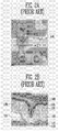
- FIG. 2a is microscopic photograph of a contact hole in an unconventional formation position
- FIG. 2b is an enlarged side view taken along line II-II' in FIG. 2a.
- contact hole 140 is electrically connected to conductive layers 120 and 130 to which the contact hole 140 must be electrically connected
- contact hole 140 is also electrically connected to conductive layer 110 to which contact hole 140 must not be electrically connected.
- FIGS. 2a and 2b when the formation position of the contact hole 140 is such that it is electrically connected to the conductive layer 110 to which the contact hole 140 must not be electrically connected, electric leakage may occur.
- a semiconductor device comprising a first insulating layer formed on a substrate, a first conductive layer formed on the first insulating layer, a second insulating layer formed on the first conductive layer, a second conductive layer formed on the second insulating layer and having a first overlapping portion overlapped with the first conductive layer, a third insulating layer formed on the second conductive layer, a third conductive layer formed on the third insulating layer and having a second overlapping portion overlapped with the second conductive layer at a position different from the position of the first overlapping portion, and a contact hole formed in either the first overlapping portion or the second overlapping portion and electrically connecting two overlapped conductive layers to each other.
- a skilled technologist will recognize that such layering and formation of further contact holes can continue as much as needed for the particular device.
- each of the conductive layers is line-shaped, minus-shaped, or crank-shaped (e.g. L, ⁇ , ⁇ , ⁇ , or ⁇ ) and has at least one extending portion which extends from the shaped configuration a predetermined width and at a predetermined angle.
- at least one of the plurality of line-shaped, minus-shaped, or crank-shaped conductive layers will have at least one extending portion extended to a predetermined width and having a predetermined angle.
- the diameter of the contact hole preferably should not exceed the width of the conductive layers.
- a method of manufacturing a semiconductor device including the steps of forming a first insulating layer on a substrate, forming a first conductive layer on the first insulating layer, forming a second insulating layer on the first conductive layer, forming a second conductive layer on the second insulating layer and having a first overlapping portion overlapped with the first conductive layer, forming a third insulating layer on the second conductive layer, forming a third conductive layer on the third insulating layer and having a second overlapping portion overlapped with the second conductive layer at a position different from the position of the first overlapping portion, and forming a contact hole either between the first overlapping portion or between the second overlapping portion and electrically connecting two overlapped conductive layers to each other.
- the third conductive layer preferably further includes a third overlapping portion overlapped with the first conductive layer at a position different from the first and second overlapping portions.
- a contact hole is preferably formed between the third overlapping portion and electrically connects two conductive layers to each other.
- the first, second, and third conductive layers are formed in a minus shape or a line shape having at least one extending portion extended to a predetermined width having a predetermined angle.
- the contact holes formed in the overlapping portions have diameters less than the widths of the overlapped conductive layers.
- the contact holes are formed by etching.
- FIG. 1A is a partial schematic plan view illustrating a conventional contact hole structure formation
- FIG. 1B is an enlarged side view taken along line I - I ' in FIG. 1A;
- FIG. 2A is a microscopic photograph of the contact hole structure in an unconventional formation position
- FIG. 2B is an enlarged side sectional view taken along the line II-II' in FIG. 2A;
- FIG. 3A is a partial schematic plan view illustrating a semiconductor device in which a contact hole is formed according to an embodiment of the present invention
- FIG. 3B is an enlarged side view taken along line III-III' in FIG. 3A;
- FIG. 4A is a partial schematic plan view illustrating a semiconductor device in which a contact hole is formed according to another embodiment of the present invention.
- FIG. 4B is an enlarged side view taken along line IV-IV' in FIG. 4A.
- FIG. 5A is a partial schematic plan view illustrating a semiconductor device in which a contact hole is formed according to yet another embodiment of the present invention.
- FIG. 5B is an enlarged side view taken along line V - V' in FIG. 5A.
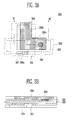
- FIG. 3 is a partial schematic plan view illustrating a semiconductor device in which a contact hole is formed according to an embodiment.
- a semiconductor device 300 includes a buffer layer (not shown) formed on a substrate (not shown), a first conductive layer 310 formed on the buffer layer, a first insulating layer 315 formed on the first conductive layer 310, a second conductive layer 320 formed on the first insulating layer 315, a second insulating layer 325 formed on the second conductive layer 320, and a third conductive layer 330 formed on the second insulating layer 325.
- the first conductive layer 310 formed on the buffer layer in the embodiment, is minus-shaped, and the first insulating layer 315 is formed on the first conductive layer 310.
- the first insulating layer 315 covers at least some region of the first conductive layer 310 such that the first conductive layer 310 does not contact the second and third conductive layers 320 and 330, respectively.
- the first insulating layer 315 has at least the same shape as the first conductive layer 310 in order to provide complete coverage of conductive layer 310.
- the second conductive layer 320 formed on the first insulating layer 315, is line-shaped and has a first overlapping portion 320a partially overlapped with the first conductive layer 310.
- the third conductive layer 330 formed on the second insulating layer 325, is cranked-shaped with at least one portion extended to a predetermined width and angle.
- FIG. 3 depicts a ⁇ -type crank-shaped third conductive layer 330.
- the third conductive layer 330 includes a second overlapping portion 330a which is overlapped with the second conductive layer 320, but is not overlapped with the first overlapping portion 320a, as well as a third overlapping portion 330b which is overlapped with the first conductive layer 310, but is not overlapped with the first overlapping portion 320a or the second overlapping portion 330a.
- contact holes may be formed for electrically connecting two of the conductive layers 310, 320, and 330 to each other conductive layer.
- the contact holes may extend into the conducting layers, for example as a result of over-etching.
- FIG. 3 depicts a contact hole 340 for electrically connecting the second conductor 320 layer to the third conductive layer 330 in the second overlapping portion 330a, although one will recognize that other configurations are possible.
- contact hole 340 may alternatively be formed in the third overlapping portion 330b or the first overlapping portion 320a.
- the widths of the conductive layers 310, 320, and 330 may be identical or different.
- the diameter of the contact hole 340 preferably does not exceed the width of the overlapped conductive layer portion within which it is formed. Particularly, when the widths of the overlapped conductive layers are different from each other, the diameter of the contact hole 340 preferably does not exceed the width of the overlapped conductive layers. This is because any misalignment may lead to etching into areas that should be insulated from the conductive layers being connected. In order to avoid unnecessary duplication, a detailed description of structure formation is omitted if it would be identical to the description provided for by the previously described embodiment.
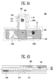
- FIG. 4 is a partial schematic plan view illustrating a semiconductor device in which a contact hole is formed according to another embodiment of the present invention.
- a semiconductor device 400 includes a buffer layer (not shown) formed on a substrate (not shown), a first conductive layer 410, a first insulating layer 415, a second conductive layer 420, a second insulating layer 425, and a third conductive layer 430.
- the first conductive layer 410 formed on the buffer layer, is ⁇ -type crank-shaped.
- the first insulating layer 415 is formed on the first conductive layer 410 to prevent the first conductive layer 410 from contacting the second conductive layer 420 and the third conductive layer 430, and to cover the first conductive layer 410.
- the second conductive layer 420 formed on the first insulating layer 415, is ⁇ -type cranked-shaped and has a first overlapping portion 420a partially overlapped with the first conductive layer 410.
- the second insulating layer 425 is formed on the second conductive layer 420 to prevent the second conductive layer 420 from directly contacting the third conductive layer 430, and to cover the second conductive layer 420.
- the third conductive layer 430 formed on either the first insulating layer 415 or the second insulating layer 425, is minus-shaped in this embodiment.
- the third conductive layer 430 includes the second overlapping portion 430a which is overlapped with the first conductive layer 410, but is not overlapped with the first overlapping portion 420a, and the third overlapping portion 430b which is overlapped with the second conductive layer 420, but is not overlapped with the first overlapping portion 420a or the second overlapping portion 430a.
- a plurality of contact holes may be formed to electrically connect two of the conductive layers 410, 420, and 430 to each other.
- a contact hole 440 is formed in the first overlapping portion 420a, where the first conductive layer 410 is overlapped with the second conductive layer 420, and electrically connects the first conductive layer 410 to the second conductive layer 420.
- a contact hole 450 is formed in the third overlapping portion 430b, where the second conductive layer 420 is overlapped with the third conductive layer 430, and electrically connects the second conductive layer 420 to the third conductive layer 430.
- the contact holes 440 and 450 generally do not have diameters that exceed the widths of the overlapped conductive layers 410 and 420 and the overlapped conductive layers 420 and 430, respectively, and are formed by etching. Moreover, not shown in the drawing, a contact hole may be further formed in the second overlapping portion 430a for electrically connecting the third conductive layer 430 and the first conductive layer 410.
- FIG. 5 is a partial schematic plan view illustrating a semiconductor device in which a contact hole is formed according to yet another embodiment of the present invention.
- the first conductive layer 510 is ⁇ -type crank-shaped.
- the first insulating layer 515 is formed on the first conductive layer 510 to prevent the first conductive layer 510 from directly contacting the second, third, and fourth conductive layers 520, 530, and 540, respectively, and to cover the first conductive layer 510.
- the second conductive layer 520 formed on the first insulating layer 515, is ⁇ -type crank-shaped and has a first overlapping portion 520a partially overlapped with the first conductive layer 410.
- the second insulating layer 525 is formed on the first conductive layer 520 to prevent the second conductive layer 520 from directly contacting the third conductive layer 530 and the fourth conductive layer 540, and to cover the second conductive layer 520.
- the third conductive layer 530 formed on either the first insulating layer 515 or the second insulating layer 525, is ⁇ -type crank-shaped in this embodiment.
- the third conductive layer 530 includes a second overlapping portion 530a which is overlapped with the second conductive layer 520.
- the third insulating layer 535 is formed on the third conductive layer 530 to prevent the third conductive layer 530 from directly contacting the fourth conductive layer 540, and to cover the third conductive layer 530.
- the fourth conductive layer 540 formed on the third conductive layer 530, is ⁇ -type crank-shaped.
- the fourth conductive layer 540 includes the third overlapping portion 540a overlapped with the third conductive layer 530 and the fourth overlapping portion 540b overlapped with the first conductive layer 510.
- a contact hole 550 is formed in the first overlapping portion 520a and electrically connects the first conductive layer 510 to the second conductive layer 520.
- a contact hole may be formed in the second overlapping portion 530a where the second conductive layer 520 is overlapped with the third conductive layer 530 to electrically connect the second conductive layer 520 to the third conductive layer 530.
- Contact holes may be further formed in the third overlapping portion 540a where the third conductive layer 530 is overlapped with the fourth conductive layer 540 to electrically connect the third conductive layer 530 to the fourth conductive layer 540 and/or in the fourth overlapping portion 540b where the first conductive layer 510 is overlapped with the fourth conductive layer 540 to electrically connect the first conductive layer 510 to the fourth conductive layer 540.
- the widths of the first, second, third, and fourth conductive layers 510, 520, 530, and 540, respectively may be identical or different.
- the contact hole 550 preferably does not have a diameter that exceeds the width of the overlapped conductive layers. If the widths of the overlapped conductive layers are different from each other, the diameter of the contact hole 550 preferably does not exceed the thinnest width of the overlapped conductive layers.
- contact holes are formed in a semiconductor device in which a plurality of conductive layers are laminated. Since another conductive layer is not present at the lower portion of the overlapping portion in which two conductive layers are overlapped, a contact hole is not formed in a position allowing deviation from the conductive layers to which the contact hole must be connected electrically, and not formed in a position where it may become electrically connected to other conductive layers to which the contact hole should not be electrically connected. Moreover, if a contact hole is not formed in the overlapping portion of two conductive layers but deviates from its predetermined position, the contact hole is very unlikely to contact another conductive layer.
Landscapes
- Internal Circuitry In Semiconductor Integrated Circuit Devices (AREA)
Abstract

Description
- The present invention relates to a semiconductor device and a manufacturing method thereof, and more particularly, to a semiconductor device capable of reducing the electrical leakage of a semiconductor device caused when a contact hole is misaligned and a manufacturing method thereof.
- Recently, in conjunction with the development of ever higher density semiconductor devices which provide greater functionality, various information devices in which semiconductor devices are installed, such as computers, mobile phones, personal digital assistants, and the like, have grown ever more popular. Semiconductors installed in these information devices are required to have a high operating speed and a great deal of storage capacity. In order to satisfy these requirements, semiconductor device manufacturing technology is developing to improve integration, reliability, and response speed.
- Moreover, as the degree of integration increases and the size of devices decrease, the distances between conductive layers forming the semiconductor devices gradually decrease. At its most basic level, the semiconductor device includes a plurality of conductive layers formed on a substrate and a plurality of insulating layers formed between the conductive layers. In order to form a semiconductor device with higher density in a more accurate way, a reduction in the thickness of the conductive layer or a reduction in the distance between the conductive layers (e.g., the thickness of the insulating layers) is typically proposed. However, by reducing the thickness of the conductive layers or the distance between the conductive layers, formation a contact hole electrically connecting the conductive layers to each other becomes more difficult.
- Hereinafter, the conventional formation of a contact hole will be described with reference to the accompanying drawings.
- FIG. 1 is a schematic plan view illustrating a conventional semiconductor device formed with a contact hole. As shown in FIG. 1, a
semiconductor device 100 includes a plurality ofconductive layers insulating layers conductive layers conductive layers contact hole 140 for electrically connecting a pair of conductive layers among theconductive layers - As shown in FIG. 1, on top of the substrate (not shown), a "line-shaped" first
conductive layer 110 is formed. When discussing "line-shaped" or "minus-shaped" conductive layers throughout the specification, the conductive layers may be a line segment or a displayed portion of a longer line, and the length, width, angle, and shape of the conductive layers are not limited to the sizes, angles, and shapes displayed by the drawings. Moreover, line-shaped and minus-shaped conductive layers may be shaped similarly, and the nomenclature is adopted only to identify the approximate orientation of the conductive layers in the drawings. Although not depicted in the drawings, a buffer layer is generally formed between the substrate and the firstconductive layer 110, and can act as an insulating layer between the substrate and the firstconductive layer 110. On top of the firstconductive layer 110, a firstinsulating layer 115 is formed to cover at least the firstconductive layer 110. On top of the firstinsulating layer 115, a minus-shaped secondconductive layer 120 overlapped with at least some portion of the firstconductive layer 110, is formed. On top of the secondconductive layer 120, a secondinsulating layer 125 is formed to cover at least some of the secondconductive layer 120. On top of the secondinsulating layer 125, a line-shaped thirdconductive layer 130 is formed at least partially overlapping the firstconductive layer 110 and the secondconductive layer 120. Within the secondinsulating layer 125, thecontact hole 140 is formed to electrically connect the secondconductive layer 120 to the thirdconductive layer 130. Thus, thecontact hole 140 electrically connects the two adjacent conductive layers to each other. - However, when a plurality of conductive layers and insulating layers between adjacent conductive layers is built using either a reduction in thickness of the conductive layers or a reduction in distance between the conductive layers, the problem shown in FIGS. 2a and 2b may occur. FIG. 2a is microscopic photograph of a contact hole in an unconventional formation position, and FIG. 2b is an enlarged side view taken along line II-II' in FIG. 2a. As shown in the drawings,
contact hole 140 is electrically connected toconductive layers contact hole 140 must be electrically connected, andcontact hole 140 is also electrically connected toconductive layer 110 to whichcontact hole 140 must not be electrically connected. Moreover, as shown in FIGS. 2a and 2b, when the formation position of thecontact hole 140 is such that it is electrically connected to theconductive layer 110 to which thecontact hole 140 must not be electrically connected, electric leakage may occur. - Accordingly, it is an aspect of the present invention to provide a semiconductor device in which the formation of the contact hole position may not deviate from the two adjacent conductive layers, which prevents electric leakage generated by such misalignment, and a manufacturing method thereof.
- According to another aspect of the invention a semiconductor device is disclosed, the semiconductor device comprising a first insulating layer formed on a substrate, a first conductive layer formed on the first insulating layer, a second insulating layer formed on the first conductive layer, a second conductive layer formed on the second insulating layer and having a first overlapping portion overlapped with the first conductive layer, a third insulating layer formed on the second conductive layer, a third conductive layer formed on the third insulating layer and having a second overlapping portion overlapped with the second conductive layer at a position different from the position of the first overlapping portion, and a contact hole formed in either the first overlapping portion or the second overlapping portion and electrically connecting two overlapped conductive layers to each other. A skilled technologist will recognize that such layering and formation of further contact holes can continue as much as needed for the particular device.
- In one embodiment, each of the conductive layers is line-shaped, minus-shaped, or crank-shaped (e.g. L, ┘, ┐, ┌, or ┴) and has at least one extending portion which extends from the shaped configuration a predetermined width and at a predetermined angle. In this embodiment, at least one of the plurality of line-shaped, minus-shaped, or crank-shaped conductive layers will have at least one extending portion extended to a predetermined width and having a predetermined angle.
- The diameter of the contact hole preferably should not exceed the width of the conductive layers.
- Other aspects of the present invention are achieved by providing a method of manufacturing a semiconductor device including the steps of forming a first insulating layer on a substrate, forming a first conductive layer on the first insulating layer, forming a second insulating layer on the first conductive layer, forming a second conductive layer on the second insulating layer and having a first overlapping portion overlapped with the first conductive layer, forming a third insulating layer on the second conductive layer, forming a third conductive layer on the third insulating layer and having a second overlapping portion overlapped with the second conductive layer at a position different from the position of the first overlapping portion, and forming a contact hole either between the first overlapping portion or between the second overlapping portion and electrically connecting two overlapped conductive layers to each other.
- The third conductive layer preferably further includes a third overlapping portion overlapped with the first conductive layer at a position different from the first and second overlapping portions. A contact hole is preferably formed between the third overlapping portion and electrically connects two conductive layers to each other. Preferably the first, second, and third conductive layers are formed in a minus shape or a line shape having at least one extending portion extended to a predetermined width having a predetermined angle. Preferably the contact holes formed in the overlapping portions have diameters less than the widths of the overlapped conductive layers. Preferably the contact holes are formed by etching.
- These and/or other aspects and advantages of the invention will become apparent and more readily appreciated from the following description of the preferred embodiments, taken in conjunction with the accompanying drawings of which:
- FIG. 1A is a partial schematic plan view illustrating a conventional contact hole structure formation;
- FIG. 1B is an enlarged side view taken along line I - I ' in FIG. 1A;
- FIG. 2A is a microscopic photograph of the contact hole structure in an unconventional formation position;
- FIG. 2B is an enlarged side sectional view taken along the line II-II' in FIG. 2A;
- FIG. 3A is a partial schematic plan view illustrating a semiconductor device in which a contact hole is formed according to an embodiment of the present invention;
- FIG. 3B is an enlarged side view taken along line III-III' in FIG. 3A;
- FIG. 4A is a partial schematic plan view illustrating a semiconductor device in which a contact hole is formed according to another embodiment of the present invention;
- FIG. 4B is an enlarged side view taken along line IV-IV' in FIG. 4A.
- FIG. 5A is a partial schematic plan view illustrating a semiconductor device in which a contact hole is formed according to yet another embodiment of the present invention; and
- FIG. 5B is an enlarged side view taken along line V - V' in FIG. 5A.
- Hereinafter, various embodiments according to aspects of the present invention will be described with reference to the accompanying drawings.
- FIG. 3 is a partial schematic plan view illustrating a semiconductor device in which a contact hole is formed according to an embodiment.
- As shown in FIG. 3, a
semiconductor device 300 includes a buffer layer (not shown) formed on a substrate (not shown), a firstconductive layer 310 formed on the buffer layer, a first insulatinglayer 315 formed on the firstconductive layer 310, a second conductive layer 320 formed on the first insulatinglayer 315, a second insulatinglayer 325 formed on the second conductive layer 320, and a thirdconductive layer 330 formed on the second insulatinglayer 325. - In addition, the first
conductive layer 310, formed on the buffer layer in the embodiment, is minus-shaped, and the first insulatinglayer 315 is formed on the firstconductive layer 310. The first insulatinglayer 315 covers at least some region of the firstconductive layer 310 such that the firstconductive layer 310 does not contact the second and thirdconductive layers 320 and 330, respectively. The first insulatinglayer 315 has at least the same shape as the firstconductive layer 310 in order to provide complete coverage ofconductive layer 310. - The second conductive layer 320, formed on the first insulating
layer 315, is line-shaped and has a first overlappingportion 320a partially overlapped with the firstconductive layer 310. The secondinsulating layer 325, formed on the second conductive layer 320, covers at least some region of the second conductive layer 320, and, in this embodiment, has at least the same shape as that of the second conductive layer 320 in order to provide complete coverage of conductive layer 320. - The third
conductive layer 330, formed on the second insulatinglayer 325, is cranked-shaped with at least one portion extended to a predetermined width and angle. FIG. 3 depicts a └-type crank-shaped thirdconductive layer 330. The thirdconductive layer 330 includes a second overlappingportion 330a which is overlapped with the second conductive layer 320, but is not overlapped with the first overlappingportion 320a, as well as a third overlappingportion 330b which is overlapped with the firstconductive layer 310, but is not overlapped with the first overlappingportion 320a or the second overlappingportion 330a. - Between each of the
conductive layers conductive layers contact hole 340 for electrically connecting the second conductor 320 layer to the thirdconductive layer 330 in the second overlappingportion 330a, although one will recognize that other configurations are possible. For example,contact hole 340 may alternatively be formed in the third overlappingportion 330b or the first overlappingportion 320a. The widths of theconductive layers contact hole 340 preferably does not exceed the width of the overlapped conductive layer portion within which it is formed. Particularly, when the widths of the overlapped conductive layers are different from each other, the diameter of thecontact hole 340 preferably does not exceed the width of the overlapped conductive layers. This is because any misalignment may lead to etching into areas that should be insulated from the conductive layers being connected. In order to avoid unnecessary duplication, a detailed description of structure formation is omitted if it would be identical to the description provided for by the previously described embodiment. - FIG. 4 is a partial schematic plan view illustrating a semiconductor device in which a contact hole is formed according to another embodiment of the present invention.
- As shown in FIG. 4, a
semiconductor device 400 includes a buffer layer (not shown) formed on a substrate (not shown), a firstconductive layer 410, a first insulatinglayer 415, a secondconductive layer 420, a second insulatinglayer 425, and a thirdconductive layer 430. - In addition, in this embodiment, the first
conductive layer 410, formed on the buffer layer, is ┘-type crank-shaped. The first insulatinglayer 415 is formed on the firstconductive layer 410 to prevent the firstconductive layer 410 from contacting the secondconductive layer 420 and the thirdconductive layer 430, and to cover the firstconductive layer 410. The secondconductive layer 420, formed on the first insulatinglayer 415, is └-type cranked-shaped and has a first overlappingportion 420a partially overlapped with the firstconductive layer 410. The secondinsulating layer 425 is formed on the secondconductive layer 420 to prevent the secondconductive layer 420 from directly contacting the thirdconductive layer 430, and to cover the secondconductive layer 420. - The third
conductive layer 430, formed on either the first insulatinglayer 415 or the second insulatinglayer 425, is minus-shaped in this embodiment. The thirdconductive layer 430 includes the second overlappingportion 430a which is overlapped with the firstconductive layer 410, but is not overlapped with the first overlappingportion 420a, and the third overlappingportion 430b which is overlapped with the secondconductive layer 420, but is not overlapped with the first overlappingportion 420a or the second overlappingportion 430a. - Between each of the
conductive layers conductive layers contact hole 440 is formed in the first overlappingportion 420a, where the firstconductive layer 410 is overlapped with the secondconductive layer 420, and electrically connects the firstconductive layer 410 to the secondconductive layer 420. Acontact hole 450 is formed in the third overlappingportion 430b, where the secondconductive layer 420 is overlapped with the thirdconductive layer 430, and electrically connects the secondconductive layer 420 to the thirdconductive layer 430. The contact holes 440 and 450 generally do not have diameters that exceed the widths of the overlappedconductive layers conductive layers portion 430a for electrically connecting the thirdconductive layer 430 and the firstconductive layer 410. - FIG. 5 is a partial schematic plan view illustrating a semiconductor device in which a contact hole is formed according to yet another embodiment of the present invention.
- As shown in FIG. 5, a
semiconductor device 500 includes a buffer layer (not shown) formed on a substrate (not shown), a firstconductive layer 510, a first insulatinglayer 515, a secondconductive layer 520, a second insulatinglayer 525, a thirdconductive layer 530, a thirdinsulating layer 535, and a fourthconductive layer 540. - In addition, in this embodiment, the first
conductive layer 510, formed on the buffer layer, is ┐-type crank-shaped. The first insulatinglayer 515 is formed on the firstconductive layer 510 to prevent the firstconductive layer 510 from directly contacting the second, third, and fourthconductive layers conductive layer 510. The secondconductive layer 520, formed on the first insulatinglayer 515, is ┌-type crank-shaped and has a first overlappingportion 520a partially overlapped with the firstconductive layer 410. The secondinsulating layer 525 is formed on the firstconductive layer 520 to prevent the secondconductive layer 520 from directly contacting the thirdconductive layer 530 and the fourthconductive layer 540, and to cover the secondconductive layer 520. - The third
conductive layer 530, formed on either the first insulatinglayer 515 or the second insulatinglayer 525, is └-type crank-shaped in this embodiment. The thirdconductive layer 530 includes a second overlappingportion 530a which is overlapped with the secondconductive layer 520. The thirdinsulating layer 535 is formed on the thirdconductive layer 530 to prevent the thirdconductive layer 530 from directly contacting the fourthconductive layer 540, and to cover the thirdconductive layer 530. The fourthconductive layer 540, formed on the thirdconductive layer 530, is ┘-type crank-shaped. The fourthconductive layer 540 includes the third overlappingportion 540a overlapped with the thirdconductive layer 530 and the fourth overlapping portion 540b overlapped with the firstconductive layer 510. - Between each of the
conductive layers contact hole 550 is formed in the first overlappingportion 520a and electrically connects the firstconductive layer 510 to the secondconductive layer 520. - Moreover, not shown in the drawing, a contact hole may be formed in the second overlapping
portion 530a where the secondconductive layer 520 is overlapped with the thirdconductive layer 530 to electrically connect the secondconductive layer 520 to the thirdconductive layer 530. Contact holes may be further formed in the third overlappingportion 540a where the thirdconductive layer 530 is overlapped with the fourthconductive layer 540 to electrically connect the thirdconductive layer 530 to the fourthconductive layer 540 and/or in the fourth overlapping portion 540b where the firstconductive layer 510 is overlapped with the fourthconductive layer 540 to electrically connect the firstconductive layer 510 to the fourthconductive layer 540. The widths of the first, second, third, and fourthconductive layers contact hole 550 preferably does not have a diameter that exceeds the width of the overlapped conductive layers. If the widths of the overlapped conductive layers are different from each other, the diameter of thecontact hole 550 preferably does not exceed the thinnest width of the overlapped conductive layers. - As described in the embodiments, contact holes are formed in a semiconductor device in which a plurality of conductive layers are laminated. Since another conductive layer is not present at the lower portion of the overlapping portion in which two conductive layers are overlapped, a contact hole is not formed in a position allowing deviation from the conductive layers to which the contact hole must be connected electrically, and not formed in a position where it may become electrically connected to other conductive layers to which the contact hole should not be electrically connected. Moreover, if a contact hole is not formed in the overlapping portion of two conductive layers but deviates from its predetermined position, the contact hole is very unlikely to contact another conductive layer.
- The structures in the embodiments of a plurality of conductive layers that are not laminated but that differ slightly in position do not limit the present invention, and are disclosed for illustrative purposes only. Moreover, overlapping portions where a plurality of layers is overlapped are described in detail for illustrative purposes only.
- Although the above-mentioned embodiments disclose structures in which three or four conductive layers are laminated, more than three or four layers can be laminated. The configuration of the laminated conductive layers is not limited to the disclosed structure.
- Although a few embodiments of the present invention have been shown and described, those skilled in the art would appreciate that changes may be made in these embodiments without departing from the principles of the invention, the scope of which is defined in the claims and their equivalents.
- As described above, the contact hole is formed in the overlapping portion formed by the overlapped conductive layers so that the contact hole is prevented from deviating from the conductive layer to which the contact hole should be electrically connected, and is prevented from being electrically connected to a conductive layer to which the contact hole should not be electrically connected. Further, electrical leakage generated by misalignment of one of the conductive layers and the contact hole can also be nearly prevented.
Claims (10)
- A semiconductor device comprising:a first insulating layer formed on a substrate;a first conductive layer formed on the first insulating layer;a second insulating layer formed on the first conductive layer;a second conductive layer formed on the second insulating layer and having a first overlapping portion that overlaps with the first conductive layer;a third insulating layer formed on the second conductive layer;a third conductive layer formed on the third insulating layer and having a second overlapping portion that overlaps with the second conductive layer at a position different from the position of the first overlapping portion; anda contact hole formed in at least one of the first overlapping portion and the second overlapping portion and electrically connecting two overlapped conductive layers to each other.
- The semiconductor device of claim 1, wherein each of the conductive layers comprises one of a minus shape, a line shape or a crank shape having at least one extending portion extended to a predetermined width having a predetermined angle.
- The semiconductor device of claim 2, wherein at least one of the conductive layers comprises a line shape having at least one extending portion extended to a predetermined width having a predetermined angle.
- The semiconductor device according to at least one of the preceding claims, wherein the diameter of the contact hole is less than the widths of the overlapped conductive layers.
- A method of manufacturing a semiconductor device, comprising:forming a first insulating layer on a substrate;forming a first conductive layer on the first insulating layer;forming a second insulating layer on the first conductive layer;forming a second conductive layer on the second insulating layer to have a first overlapping portion that overlaps with the first conductive layer;forming a third insulating layer on the second conductive layer;forming a third conductive layer on the third insulating layer to have a second overlapping portion that overlaps with the second conductive layer at a position different from the position of the first overlapping portion; andforming a contact hole in at least one of the first overlapping portion and the second overlapping portion and electrically connecting two overlapped conductive layers to each other.
- The method of claim 5, wherein the third conductive layer is formed so as to comprise a third overlapping portion overlapped with the first conductive layer at a position different from the positions of the first and second overlapping portions.
- The method according to at least one of claims 5 or 6, further comprising the step of forming a contact hole for electrically connecting two conductive layers formed in the third overlapping portion.
- The method according to at least one of claims 5 - 7, wherein the first, second, and third conductive layers are formed in a minus shape, a crank shape or a line shape having at least one extending portion extended to a predetermined width having a predetermined angle.
- The according to at least one of claims 5-8, wherein the contact holes formed in the overlapping portions have diameters less than the widths of the overlapped conductive layers.
- The according to at least one of claims 5 - 9, wherein the contact holes are formed by etching.
Applications Claiming Priority (1)
| Application Number | Priority Date | Filing Date | Title |
|---|---|---|---|
| KR1020050039534A KR100645721B1 (en) | 2005-05-11 | 2005-05-11 | Semiconductor device and manufacturing method thereof |
Publications (2)
| Publication Number | Publication Date |
|---|---|
| EP1722415A2 true EP1722415A2 (en) | 2006-11-15 |
| EP1722415A3 EP1722415A3 (en) | 2007-03-14 |
Family
ID=36717119
Family Applications (1)
| Application Number | Title | Priority Date | Filing Date |
|---|---|---|---|
| EP06112404A Withdrawn EP1722415A3 (en) | 2005-05-11 | 2006-04-10 | Semiconductor device and manufacturing method thereof |
Country Status (5)
| Country | Link |
|---|---|
| US (1) | US7432598B2 (en) |
| EP (1) | EP1722415A3 (en) |
| JP (1) | JP4663530B2 (en) |
| KR (1) | KR100645721B1 (en) |
| CN (1) | CN1862803A (en) |
Families Citing this family (1)
| Publication number | Priority date | Publication date | Assignee | Title |
|---|---|---|---|---|
| KR20110002261A (en) | 2009-07-01 | 2011-01-07 | 삼성전자주식회사 | Semiconductor devices including dummy |
Citations (1)
| Publication number | Priority date | Publication date | Assignee | Title |
|---|---|---|---|---|
| JPH03163828A (en) * | 1989-11-21 | 1991-07-15 | Nec Corp | Semiconductor device |
Family Cites Families (15)
| Publication number | Priority date | Publication date | Assignee | Title |
|---|---|---|---|---|
| JPS63260054A (en) * | 1987-04-16 | 1988-10-27 | Nec Corp | Semiconductor integrated circuit device |
| JPS6484642A (en) * | 1987-09-26 | 1989-03-29 | Nec Corp | Semiconductor device equipped with multilayer interconnection structure |
| JPS6490544A (en) * | 1987-10-01 | 1989-04-07 | Matsushita Electronics Corp | Semiconductor integrated circuit |
| JPH03234020A (en) * | 1990-02-09 | 1991-10-18 | Fujitsu Ltd | Manufacture of semiconductor device |
| JPH03263855A (en) * | 1990-03-14 | 1991-11-25 | Mitsubishi Electric Corp | Multilayer wiring structure |
| JPH0711021B2 (en) | 1990-08-02 | 1995-02-08 | 三菱重工業株式会社 | Method for spheroidizing molten cast iron |
| JPH0493048A (en) * | 1990-08-09 | 1992-03-25 | Seiko Epson Corp | semiconductor equipment |
| JPH04355951A (en) * | 1991-02-06 | 1992-12-09 | Hitachi Vlsi Eng Corp | Semiconductor device and manufacture thereof |
| KR950001155B1 (en) | 1991-12-30 | 1995-02-11 | 삼정전자 주식회사 | Manufacturing method of semiconductor device |
| KR950011555B1 (en) * | 1992-06-16 | 1995-10-06 | 현대전자산업주식회사 | Contact structure and manufacturing method thereof |
| JPH07312415A (en) * | 1994-05-16 | 1995-11-28 | Yamaha Corp | Semiconductor integrated circuit |
| JPH08124928A (en) * | 1994-10-21 | 1996-05-17 | Nec Corp | Semiconductor integrated circuit |
| KR19980031103A (en) * | 1996-10-31 | 1998-07-25 | 김영환 | Manufacturing method of semiconductor device |
| JP3406865B2 (en) * | 1999-07-22 | 2003-05-19 | 沖電気工業株式会社 | Connection structure |
| KR100534096B1 (en) * | 2003-06-24 | 2005-12-06 | 삼성전자주식회사 | Fuse region of a semiconductor memory device and method of fabricating the same |
-
2005
- 2005-05-11 KR KR1020050039534A patent/KR100645721B1/en not_active Expired - Lifetime
-
2006
- 2006-01-12 JP JP2006005245A patent/JP4663530B2/en not_active Expired - Lifetime
- 2006-04-10 EP EP06112404A patent/EP1722415A3/en not_active Withdrawn
- 2006-04-29 CN CNA2006100790848A patent/CN1862803A/en active Pending
- 2006-05-09 US US11/430,814 patent/US7432598B2/en not_active Expired - Lifetime
Patent Citations (1)
| Publication number | Priority date | Publication date | Assignee | Title |
|---|---|---|---|---|
| JPH03163828A (en) * | 1989-11-21 | 1991-07-15 | Nec Corp | Semiconductor device |
Also Published As
| Publication number | Publication date |
|---|---|
| US7432598B2 (en) | 2008-10-07 |
| US20060275622A1 (en) | 2006-12-07 |
| JP2006319307A (en) | 2006-11-24 |
| KR100645721B1 (en) | 2006-11-14 |
| JP4663530B2 (en) | 2011-04-06 |
| CN1862803A (en) | 2006-11-15 |
| EP1722415A3 (en) | 2007-03-14 |
Similar Documents
| Publication | Publication Date | Title |
|---|---|---|
| KR101503876B1 (en) | Nonvolatile memory element | |
| US7595522B2 (en) | Nonvolatile semiconductor memory | |
| US20120168905A1 (en) | Capacitor of nonvolatile memory device | |
| US20230125309A1 (en) | Semiconductor device and method for preparing same | |
| US11476276B2 (en) | Semiconductor device and method for fabricating the same | |
| US20250087531A1 (en) | Semiconductor chip structure | |
| US12108598B2 (en) | Semiconductor storage device with pillar | |
| US20090305495A1 (en) | Semiconductor device and methods of manufacturing the same | |
| CN114078809B (en) | Capacitor structure and manufacturing method thereof | |
| CN119092529A (en) | A shallow trench isolation structure and semiconductor device | |
| US8222742B2 (en) | Semiconductor device | |
| JP3109478B2 (en) | Semiconductor device | |
| JP2004072109A (en) | Integrated circuit having insulating spacer extended below conductive line and method of manufacturing the same | |
| US7432598B2 (en) | Semiconductor device | |
| JPH1197525A (en) | Semiconductor device and manufacturing method thereof | |
| CN115206983A (en) | Semiconductor memory device having channel plug | |
| CN118263214B (en) | Semiconductor structure and manufacturing method thereof | |
| US20250096152A1 (en) | Semiconductor device and method of manufacturing semiconductor device | |
| CN114188333B (en) | A semiconductor memory and its fabrication method, and an electronic device thereof. | |
| US8847301B2 (en) | Semiconductor device and method for manufacturing semiconductor device | |
| CN114141825B (en) | Display panel and mobile terminal | |
| US7964906B2 (en) | Semiconductor device and method of manufacturing same | |
| CN120166716B (en) | Memory and its manufacturing method, electronic devices | |
| US7902592B2 (en) | Semiconductor device and method for manufacturing | |
| CN113782512A (en) | Display panel and mobile terminal |
Legal Events
| Date | Code | Title | Description |
|---|---|---|---|
| PUAI | Public reference made under article 153(3) epc to a published international application that has entered the european phase |
Free format text: ORIGINAL CODE: 0009012 |
|
| 17P | Request for examination filed |
Effective date: 20060410 |
|
| AK | Designated contracting states |
Kind code of ref document: A2 Designated state(s): AT BE BG CH CY CZ DE DK EE ES FI FR GB GR HU IE IS IT LI LT LU LV MC NL PL PT RO SE SI SK TR |
|
| AX | Request for extension of the european patent |
Extension state: AL BA HR MK YU |
|
| PUAL | Search report despatched |
Free format text: ORIGINAL CODE: 0009013 |
|
| AK | Designated contracting states |
Kind code of ref document: A3 Designated state(s): AT BE BG CH CY CZ DE DK EE ES FI FR GB GR HU IE IS IT LI LT LU LV MC NL PL PT RO SE SI SK TR |
|
| AX | Request for extension of the european patent |
Extension state: AL BA HR MK YU |
|
| 17Q | First examination report despatched |
Effective date: 20070302 |
|
| AKX | Designation fees paid |
Designated state(s): DE FR GB |
|
| RAP1 | Party data changed (applicant data changed or rights of an application transferred) |
Owner name: SAMSUNG MOBILE DISPLAY CO., LTD. |
|
| STAA | Information on the status of an ep patent application or granted ep patent |
Free format text: STATUS: THE APPLICATION IS DEEMED TO BE WITHDRAWN |
|
| 18D | Application deemed to be withdrawn |
Effective date: 20120103 |