EP1718932B1 - Series bridge circuit - Google Patents
Series bridge circuit Download PDFInfo
- Publication number
- EP1718932B1 EP1718932B1 EP05723920A EP05723920A EP1718932B1 EP 1718932 B1 EP1718932 B1 EP 1718932B1 EP 05723920 A EP05723920 A EP 05723920A EP 05723920 A EP05723920 A EP 05723920A EP 1718932 B1 EP1718932 B1 EP 1718932B1
- Authority
- EP
- European Patent Office
- Prior art keywords
- coupled
- circuit
- bridge
- transducer
- pair
- Prior art date
- Legal status (The legal status is an assumption and is not a legal conclusion. Google has not performed a legal analysis and makes no representation as to the accuracy of the status listed.)
- Expired - Fee Related
Links
Images


Classifications
-
- G—PHYSICS
- G01—MEASURING; TESTING
- G01D—MEASURING NOT SPECIALLY ADAPTED FOR A SPECIFIC VARIABLE; ARRANGEMENTS FOR MEASURING TWO OR MORE VARIABLES NOT COVERED IN A SINGLE OTHER SUBCLASS; TARIFF METERING APPARATUS; MEASURING OR TESTING NOT OTHERWISE PROVIDED FOR
- G01D5/00—Mechanical means for transferring the output of a sensing member; Means for converting the output of a sensing member to another variable where the form or nature of the sensing member does not constrain the means for converting; Transducers not specially adapted for a specific variable
- G01D5/12—Mechanical means for transferring the output of a sensing member; Means for converting the output of a sensing member to another variable where the form or nature of the sensing member does not constrain the means for converting; Transducers not specially adapted for a specific variable using electric or magnetic means
- G01D5/14—Mechanical means for transferring the output of a sensing member; Means for converting the output of a sensing member to another variable where the form or nature of the sensing member does not constrain the means for converting; Transducers not specially adapted for a specific variable using electric or magnetic means influencing the magnitude of a current or voltage
- G01D5/142—Mechanical means for transferring the output of a sensing member; Means for converting the output of a sensing member to another variable where the form or nature of the sensing member does not constrain the means for converting; Transducers not specially adapted for a specific variable using electric or magnetic means influencing the magnitude of a current or voltage using Hall-effect devices
-
- G—PHYSICS
- G01—MEASURING; TESTING
- G01D—MEASURING NOT SPECIALLY ADAPTED FOR A SPECIFIC VARIABLE; ARRANGEMENTS FOR MEASURING TWO OR MORE VARIABLES NOT COVERED IN A SINGLE OTHER SUBCLASS; TARIFF METERING APPARATUS; MEASURING OR TESTING NOT OTHERWISE PROVIDED FOR
- G01D3/00—Indicating or recording apparatus with provision for the special purposes referred to in the subgroups
- G01D3/02—Indicating or recording apparatus with provision for the special purposes referred to in the subgroups with provision for altering or correcting the law of variation
- G01D3/021—Indicating or recording apparatus with provision for the special purposes referred to in the subgroups with provision for altering or correcting the law of variation using purely analogue techniques
-
- H—ELECTRICITY
- H03—ELECTRONIC CIRCUITRY
- H03F—AMPLIFIERS
- H03F3/00—Amplifiers with only discharge tubes or only semiconductor devices as amplifying elements
- H03F3/181—Low frequency amplifiers, e.g. audio preamplifiers
-
- H—ELECTRICITY
- H03—ELECTRONIC CIRCUITRY
- H03F—AMPLIFIERS
- H03F3/00—Amplifiers with only discharge tubes or only semiconductor devices as amplifying elements
- H03F3/45—Differential amplifiers
- H03F3/45071—Differential amplifiers with semiconductor devices only
-
- H—ELECTRICITY
- H03—ELECTRONIC CIRCUITRY
- H03F—AMPLIFIERS
- H03F2203/00—Indexing scheme relating to amplifiers with only discharge tubes or only semiconductor devices as amplifying elements covered by H03F3/00
- H03F2203/45—Indexing scheme relating to differential amplifiers
- H03F2203/45361—Indexing scheme relating to differential amplifiers the AAC comprising multiple transistors parallel coupled at their drains only, e.g. in a cascode dif amp, only those forming the composite common source transistor
Definitions
- the present invention relates to circuits, and in particular to a series bridge circuit in a complimentary push-pull configuration.
- the Hall effect occurs when a conductor carrying current is placed in a magnetic field. A voltage is generated according to the cross product of the field and flow of current. Sensors operating on the Hall effect can be modeled like a Wheatstone bridge. Multiple sensors may be used in parallel, and are typically coupled to a differential amplifier to measure the generated voltage. To reduce current, several different implementations of bridges have been used, including thin conducting layers, commutation of a single bridge, or modifying the duty cycle of the bridges. These arrangements increase the complexity and cost of the sensor.
- US6104187A discloses a magnetoresistive sensor with temperature-stable zero point.
- US3497824A discloses a differential amplifier.
- Two bridge type transducers are coupled in series with their amplifier outputs tied together.
- the outputs are tied together in a push-pull configuration.
- push-pull operation is obtained by matching amplifier gain components and using current mirrors. Lower voltage operation may be achieved by simple diode level shifting of the transducer outputs.
- the transducers comprise Hall effect sensors.
- a bridge amplifier circuit is shown generally at 100 in FIG. 1 .
- the bridge amplifier circuit 100 comprises a first bridge circuit 110 coupled in series with a second bridge circuit 115 and with a regulated voltage 120 to provide a current flowing through the bridges.
- the bridge circuits comprise Hall effect transducers, which may be represented as Wheatstone bridges, having four resistors coupled in a diamond shape.
- Bridge 110 comprises four resistors coupled between points 125, 126, 127 and 128, and bridge 115 comprises four resistors coupled between points 130, 131, 132, and 133.
- the regulated voltage 120 is coupled to point 130, through resistors to points 131 and 133, and then through further resistors to point 132.
- Point 132 is coupled to point 125, through resistors to points 126 and 128, and through further resistors to point 127, and ground.
- a first differential amplifier is coupled to the first bridge circuit 110 and comprises a pair of transistors 140 and 141, each having a base or input coupled to points 128 and 126 respectively.
- transistors 140 and 141 are npn transistors.
- a second differential amplifier is coupled to the second bridge circuit 115 and comprises a pair of transistors 145 and 146, each having a base or input coupled to points 133 and 131 respectively.
- transistors 145 and 146 are pnp transistors.
- Collectors of transistors 140 and 145 are coupled to a first output 150.
- the loads comprise resistors.
- Current flowing through emitters of the transistors are represented at 170 and 175 labeled I E .
- Current 170 is effectively sourced from a supply, and current 175 is sinking to ground.
- the gain of the circuit is proportional to the resistance of the total load, and I E .
- the differential amplifiers are coupled in a push-pull configuration, where points 128 and 133 are negative, and points 126 and 131 are positive.
- the push-pull configuration effectively doubles the gain of the circuit compared to each half circuit and allows a large dynamic range on the output.
- the circuit is also fairly simple, reducing the complexity and cost of manufacture.
- the circuit 100 is formed on a semiconductor substrate, and the distance between bridges 110 and 115 may be varied significantly depending on whether it is necessary to sense a common mode versus differential magnetic field.
- FIG. 2 is a modified circuit 200 for improved gain/common mode offset properties. Like elements are numbered the same as in FIG. 1 .
- current mirrors 210, 215 and 220, 225 are added to a npn differential pair of transistors 245 and 246 respectively. Emitters of transistors 245 and 246 have a bias current 230 to ground.
- the current mirrors each comprise a pair of transistors having their bases coupled to each other and to the collector of the respective differential transistors 245 and 246.
- the collector of current mirror transistor 215 is also coupled to the bases of the transistors 210 and 215.
- the collector of transistor 210 is coupled to output 150, while the emitters of both transistors 210 and 215 are coupled, and produce approximately twice the emitter current 170 of the circuit of FIG. 1 .
- the top differential pair of transistors 245 and 246 are npn transistors, and the polarity of the top bridge is reversed. Transconductance of the top and bottom portions of the circuit 100 are substantially balanced.
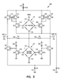
- FIG 3 is a modified circuit 300, wherein the bridges have the same polarity as in FIG. 2 .
- Circuit 300 has the same current mirror arrangement for the top bridge 115, but has a pair of level shifting devices 310 and 315 to provide for lower voltage operation of circuit 300 by reducing the number of V BE drops required for placing the differential amplifiers in the proper operating ranges.
- level shifting device 310 and 315 comprise pnp transistors, each having a base coupled to opposite corners of the bottom bridge 110. Their collectors are coupled to ground, and their emitters are coupled to respective current sources 320 and 325, as well as to respective bases of differential transistors 140 and 141.
- diodes or other devices may be used to provide the level shifting, and alternative processing technologies such as CMOS or BiCMOS may be used to implement the present invention.
- CMOS complementary metal-oxide
- BiCMOS BiCMOS
- the transducers are arranged in series, across a regulator or supply.
- the transducers may be Hall effect devices or any general Wheatstone bridge transducer arrangement.
- Each transducer feeds a differential input type stage, with a lower stage sinking current towards ground, and the other sourcing current from the supply. While the differential input stages are represented as simple transistors, many different implementations of such stages may be used.
- the outputs are tied together in a push-pull configuration.
- the input polarity of the transducers is dependent on whether the transducers are to be collocated or separated in a differential transducer configuration.
- the gain can be limited or temperature compensated by placing appropriate loads, such as resistors from each output to a reference voltage, and by adjusting the tail current level and associated temperature coefficient.
- the circuit may be implemented within monolithic silicon integrated circuits, using bipolar technology with Hall effect, magnetoresistive or piezoresistive sensing elements.
Abstract
Description
- The present invention relates to circuits, and in particular to a series bridge circuit in a complimentary push-pull configuration.
- The Hall effect occurs when a conductor carrying current is placed in a magnetic field. A voltage is generated according to the cross product of the field and flow of current. Sensors operating on the Hall effect can be modeled like a Wheatstone bridge. Multiple sensors may be used in parallel, and are typically coupled to a differential amplifier to measure the generated voltage. To reduce current, several different implementations of bridges have been used, including thin conducting layers, commutation of a single bridge, or modifying the duty cycle of the bridges. These arrangements increase the complexity and cost of the sensor.
-
US6104187A discloses a magnetoresistive sensor with temperature-stable zero point.US3497824A discloses a differential amplifier. - Two bridge type transducers are coupled in series with their amplifier outputs tied together. In one embodiment, the outputs are tied together in a push-pull configuration. In further embodiments, push-pull operation is obtained by matching amplifier gain components and using current mirrors. Lower voltage operation may be achieved by simple diode level shifting of the transducer outputs. In one embodiment, the transducers comprise Hall effect sensors.
-
FIG. 1 is a circuit diagram of a pair of series connected bridge type transducers according to an embodiment of the invention. -
FIG. 2 is a circuit diagram of an alternative pair of series connected bridge type transducers according to an embodiment of the invention. -
FIG. 3 is a circuit diagram of a further alternative pair of series connected bridge type transducers according to an embodiment of the invention. - In the following description, reference is made to the accompanying drawings that form a part hereof, and in which is shown by way of illustration specific embodiments in which the invention may be practiced. These embodiments are described in sufficient detail to enable those skilled in the art to practice the invention, and it is to be understood that other embodiments may be utilized and that structural, logical and electrical changes may be made without departing from the scope of the present invention. The following description is, therefore, not to be taken in a limited sense, and the scope of the present invention is defined by the appended claims.
- A bridge amplifier circuit is shown generally at 100 in
FIG. 1 . Thebridge amplifier circuit 100 comprises afirst bridge circuit 110 coupled in series with asecond bridge circuit 115 and with a regulatedvoltage 120 to provide a current flowing through the bridges. In one embodiment, the bridge circuits comprise Hall effect transducers, which may be represented as Wheatstone bridges, having four resistors coupled in a diamond shape.Bridge 110 comprises four resistors coupled betweenpoints bridge 115 comprises four resistors coupled betweenpoints - In
FIG. 1 , the regulatedvoltage 120 is coupled topoint 130, through resistors topoints point 132.Point 132 is coupled topoint 125, through resistors topoints point 127, and ground. - A first differential amplifier is coupled to the
first bridge circuit 110 and comprises a pair oftransistors points transistors second bridge circuit 115 and comprises a pair oftransistors points transistors transistors first output 150. Collectors oftransistors second output 155. Theoutputs points respective loads - In one embodiment, the differential amplifiers are coupled in a push-pull configuration, where
points points - In one embodiment, the
circuit 100 is formed on a semiconductor substrate, and the distance betweenbridges -
FIG. 2 is a modifiedcircuit 200 for improved gain/common mode offset properties. Like elements are numbered the same as inFIG. 1 . In this embodiment,current mirrors transistors transistors differential transistors current mirror transistor 215 is also coupled to the bases of thetransistors transistor 210 is coupled tooutput 150, while the emitters of bothtransistors emitter current 170 of the circuit ofFIG. 1 . In this embodiment, the top differential pair oftransistors circuit 100 are substantially balanced.FIG 3 is a modifiedcircuit 300, wherein the bridges have the same polarity as inFIG. 2 .Circuit 300 has the same current mirror arrangement for thetop bridge 115, but has a pair oflevel shifting devices circuit 300 by reducing the number of VBE drops required for placing the differential amplifiers in the proper operating ranges. In one embodiment,level shifting device bottom bridge 110. Their collectors are coupled to ground, and their emitters are coupled to respectivecurrent sources differential transistors individual bridges - Two transducers are arranged in series, across a regulator or supply. The transducers may be Hall effect devices or any general Wheatstone bridge transducer arrangement. Each transducer feeds a differential input type stage, with a lower stage sinking current towards ground, and the other sourcing current from the supply. While the differential input stages are represented as simple transistors, many different implementations of such stages may be used. The outputs are tied together in a push-pull configuration. The input polarity of the transducers is dependent on whether the transducers are to be collocated or separated in a differential transducer configuration. The gain can be limited or temperature compensated by placing appropriate loads, such as resistors from each output to a reference voltage, and by adjusting the tail current level and associated temperature coefficient. Common mode improvements are made by matching the amplifier gain components and using current mirrors to achieve the push-pull operation. Lower voltage operation can be achieved by simple diode level shifting of the transducer outputs. In further embodiments, the circuit may be implemented within monolithic silicon integrated circuits, using bipolar technology with Hall effect, magnetoresistive or piezoresistive sensing elements.
Claims (8)
- A circuit (100, 200, 300) comprising:a first bridge transducer (110);a second bridge transducer (115) coupled in series with the first bridge transducer (110) and a supply (120);a first differential amplifier (140, 141) having inputs coupled to the first bridge transducer; anda second differential amplifier (145, 146, 245, 246) having inputs coupled to the second bridge transducer, wherein the first and second differential amplifiers each have a pair of outputs, respective ones of which are coupled to provide two outputs (150, 155) of the circuit representative of a sensed parameter, and wherein the first and second differential amplifiers (140, 141 and 145, 146, 256, 246) are coupled in a push-pull relationship.
- The circuit of claim 1 wherein the first and second bridge transducers (110, 115) comprise Hall effect sensors.
- The circuit of claim 1 wherein the supply (120) comprise a regulated voltage.
- The circuit of claim 1 wherein the first differential amplifier (140, 141) comprises a pair of npn transistors and the second differential amplifier (145, 146, 245, 246) comprises a pair of pnp transistors.
- The circuit of claim 1 wherein the output comprises a load (160, 165) coupled between the outputs.
- The circuit of claim 1 and further comprising:a load (160, 165) coupled between the two outputs (150, 155) and a point where the first and second bridge transducers are coupled;a pair of current mirrors (210, 215 and 220, 225) coupled to the second differential amplifier (145, 146, 245, 246); anda pair of level shift transistors (310, 315) coupled between the first differential amplifier (140, 141) and the first bridge transducer (110).
- The circuit of claim 6, wherein the differential amplifiers (140, 141 and 145, 146, 256, 246) each comprise a pair of npn transistors, and wherein the npn transistors of the second differential amplifier (145, 146, 245, 246) each have a base coupled to opposite corners of the second bridge transducer (115), have a collector coupled to the current mirror (210, 215 and 220, 225) and have an emitter coupled to a supply (120) sinking current to ground, and wherein the npn transistors of the first differential amplifier (140, 141) each have a base coupled to opposite corners of the first bridge transducer (110) through the level shift transistors (310, 315), and have a emitters coupled to current sources (320, 325).
- A method comprising:sensing a magnetic field with a first Hall effect transducer (110);sensing a magnetic field with a second Hall effect transducer (115) coupled in series with the first Hall effect transducer (110) and a supply (120);amplifying the sensed magnetic fields with a pair of differential amplifiers (140, 141 and 145, 146, 256, 246) having outputs (150, 155) tied together in a push-pull configuration.
Applications Claiming Priority (2)
| Application Number | Priority Date | Filing Date | Title |
|---|---|---|---|
| US10/789,070 US7005915B2 (en) | 2004-02-27 | 2004-02-27 | Series bridge circuit with amplifiers |
| PCT/US2005/006255 WO2005085764A2 (en) | 2004-02-27 | 2005-02-25 | Series bridge circuit |
Publications (2)
| Publication Number | Publication Date |
|---|---|
| EP1718932A2 EP1718932A2 (en) | 2006-11-08 |
| EP1718932B1 true EP1718932B1 (en) | 2011-02-09 |
Family
ID=34887171
Family Applications (1)
| Application Number | Title | Priority Date | Filing Date |
|---|---|---|---|
| EP05723920A Expired - Fee Related EP1718932B1 (en) | 2004-02-27 | 2005-02-25 | Series bridge circuit |
Country Status (6)
| Country | Link |
|---|---|
| US (1) | US7005915B2 (en) |
| EP (1) | EP1718932B1 (en) |
| JP (1) | JP4498414B2 (en) |
| CN (1) | CN100529673C (en) |
| DE (1) | DE602005026256D1 (en) |
| WO (1) | WO2005085764A2 (en) |
Families Citing this family (6)
| Publication number | Priority date | Publication date | Assignee | Title |
|---|---|---|---|---|
| US7279891B1 (en) | 2006-06-15 | 2007-10-09 | Honeywell International Inc. | Permalloy bridge with selectable wafer-anistropy using multiple layers |
| FR3031586B1 (en) * | 2015-01-13 | 2017-02-10 | Dymeo | INDUCTIVE DISPLACEMENT SENSORS |
| CN105371877B (en) * | 2015-10-28 | 2017-11-10 | 深圳市志奋领科技有限公司 | Switch-type sensor detects circuit |
| US10260981B2 (en) * | 2017-02-06 | 2019-04-16 | Nxp Usa, Inc. | Pressure sensor having sense elements in multiple wheatstone bridges with chained outputs |
| US10897234B2 (en) * | 2019-03-22 | 2021-01-19 | Stmicroelectronics S.R.L. | Fully differential operational amplifier common mode current sensing feedback |
| US11422044B2 (en) | 2020-05-19 | 2022-08-23 | Stmicroelectronics S.R.L. | Resistive bridge sensor with temperature compensation |
Family Cites Families (11)
| Publication number | Priority date | Publication date | Assignee | Title |
|---|---|---|---|---|
| US3497824A (en) * | 1967-08-18 | 1970-02-24 | Bell Telephone Labor Inc | Differential amplifier |
| US5337013A (en) * | 1992-06-10 | 1994-08-09 | Ford Motor Company | Method and apparatus for monitoring the operation of electrical loads in an automotive vehicle |
| DE19543564A1 (en) * | 1994-11-22 | 1996-05-23 | Bosch Gmbh Robert | Non-contact rotary angle determn. appts for rotating element |
| DE19640695A1 (en) * | 1996-10-02 | 1998-04-09 | Bosch Gmbh Robert | Magnetoresistive sensor with temperature-stable zero point |
| US5834952A (en) * | 1996-10-10 | 1998-11-10 | Vtc Inc. | Open-loop current mode biasing scheme for MR head |
| US6195228B1 (en) * | 1997-01-06 | 2001-02-27 | Nec Research Institute, Inc. | Thin, horizontal-plane hall sensors for read-heads in magnetic recording |
| EP0877228B1 (en) * | 1997-05-09 | 2003-08-06 | Tesa Sa | Magnetoresistance sensor for measuring dimensions |
| US6104197A (en) * | 1997-06-02 | 2000-08-15 | Tektronix, Inc. | Apparatus for acquiring waveform data from a metallic transmission cable |
| DE19757196A1 (en) * | 1997-12-22 | 1999-06-24 | Philips Patentverwaltung | Sensor arrangement with measurement error detection |
| US6445171B2 (en) * | 1999-10-29 | 2002-09-03 | Honeywell Inc. | Closed-loop magnetoresistive current sensor system having active offset nulling |
| US6577187B1 (en) * | 2000-06-15 | 2003-06-10 | Upstate Audio | Powered transducer preamplifier with DC level shifting circuit |
-
2004
- 2004-02-27 US US10/789,070 patent/US7005915B2/en not_active Expired - Fee Related
-
2005
- 2005-02-25 JP JP2007501046A patent/JP4498414B2/en not_active Expired - Fee Related
- 2005-02-25 CN CNB2005800058196A patent/CN100529673C/en not_active Expired - Fee Related
- 2005-02-25 EP EP05723920A patent/EP1718932B1/en not_active Expired - Fee Related
- 2005-02-25 DE DE602005026256T patent/DE602005026256D1/en active Active
- 2005-02-25 WO PCT/US2005/006255 patent/WO2005085764A2/en active Application Filing
Also Published As
| Publication number | Publication date |
|---|---|
| CN1922466A (en) | 2007-02-28 |
| WO2005085764A3 (en) | 2005-11-10 |
| US20050189988A1 (en) | 2005-09-01 |
| EP1718932A2 (en) | 2006-11-08 |
| DE602005026256D1 (en) | 2011-03-24 |
| JP4498414B2 (en) | 2010-07-07 |
| WO2005085764A2 (en) | 2005-09-15 |
| JP2007525678A (en) | 2007-09-06 |
| US7005915B2 (en) | 2006-02-28 |
| CN100529673C (en) | 2009-08-19 |
Similar Documents
| Publication | Publication Date | Title |
|---|---|---|
| US4760285A (en) | Hall effect device with epitaxal layer resistive means for providing temperature independent sensitivity | |
| EP1718932B1 (en) | Series bridge circuit | |
| JPH01143510A (en) | Two-terminal temperture compensation type current source circuit | |
| JPH04369878A (en) | Magnetoresistance effect element circuit | |
| US5323120A (en) | High swing operational transconductance amplifier | |
| US4683429A (en) | Electrical circuit which is linearly responsive to changes in magnetic field intensity | |
| EP0164182B1 (en) | Jfet active load input stage | |
| EP3168576B1 (en) | Differential amplifier for hall effect bridge transducer | |
| ES2329869T3 (en) | IMPROVED OUTPUT STAGE OF AN OPERATIONAL AMPLIFIER. | |
| US20040108888A1 (en) | Constant voltage generating circuit | |
| JPS62293385A (en) | Addition amplifier | |
| JP2776318B2 (en) | Operational amplifier circuit | |
| US5631608A (en) | Driver for N-channel VFET output stage of power amplifier | |
| JP2503913B2 (en) | Differential amplifier | |
| US6307434B1 (en) | Circuit for ensuring full saturation of amplifiers of a single input configured bridge amplifier | |
| JPH08114659A (en) | Semiconductor magnetoelectric transducer | |
| JPS6017939Y2 (en) | integrated circuit device | |
| JPS5918368Y2 (en) | Current detection circuits such as power amplifier circuits | |
| JPS63133707A (en) | Differential amplifier circuit | |
| JP2797322B2 (en) | amplifier | |
| JP2703953B2 (en) | Current amplifier circuit | |
| JPH04236382A (en) | Integrated magnetoresistance effect element circuit | |
| JPH0474887B2 (en) | ||
| TWI232633B (en) | Temperature and voltage compensated Hall sensor circuit | |
| JPH05299947A (en) | Differential amplifier |
Legal Events
| Date | Code | Title | Description |
|---|---|---|---|
| PUAI | Public reference made under article 153(3) epc to a published international application that has entered the european phase |
Free format text: ORIGINAL CODE: 0009012 |
|
| 17P | Request for examination filed |
Effective date: 20060825 |
|
| AK | Designated contracting states |
Kind code of ref document: A2 Designated state(s): DE FR GB |
|
| DAX | Request for extension of the european patent (deleted) | ||
| RBV | Designated contracting states (corrected) |
Designated state(s): DE FR GB |
|
| 17Q | First examination report despatched |
Effective date: 20100503 |
|
| GRAP | Despatch of communication of intention to grant a patent |
Free format text: ORIGINAL CODE: EPIDOSNIGR1 |
|
| GRAS | Grant fee paid |
Free format text: ORIGINAL CODE: EPIDOSNIGR3 |
|
| GRAA | (expected) grant |
Free format text: ORIGINAL CODE: 0009210 |
|
| AK | Designated contracting states |
Kind code of ref document: B1 Designated state(s): DE FR GB |
|
| REG | Reference to a national code |
Ref country code: GB Ref legal event code: FG4D |
|
| REF | Corresponds to: |
Ref document number: 602005026256 Country of ref document: DE Date of ref document: 20110324 Kind code of ref document: P |
|
| REG | Reference to a national code |
Ref country code: DE Ref legal event code: R096 Ref document number: 602005026256 Country of ref document: DE Effective date: 20110324 |
|
| PLBE | No opposition filed within time limit |
Free format text: ORIGINAL CODE: 0009261 |
|
| STAA | Information on the status of an ep patent application or granted ep patent |
Free format text: STATUS: NO OPPOSITION FILED WITHIN TIME LIMIT |
|
| 26N | No opposition filed |
Effective date: 20111110 |
|
| REG | Reference to a national code |
Ref country code: DE Ref legal event code: R097 Ref document number: 602005026256 Country of ref document: DE Effective date: 20111110 |
|
| PGFP | Annual fee paid to national office [announced via postgrant information from national office to epo] |
Ref country code: FR Payment date: 20120203 Year of fee payment: 8 |
|
| PGFP | Annual fee paid to national office [announced via postgrant information from national office to epo] |
Ref country code: DE Payment date: 20120229 Year of fee payment: 8 |
|
| PGFP | Annual fee paid to national office [announced via postgrant information from national office to epo] |
Ref country code: GB Payment date: 20120127 Year of fee payment: 8 |
|
| GBPC | Gb: european patent ceased through non-payment of renewal fee |
Effective date: 20130225 |
|
| REG | Reference to a national code |
Ref country code: FR Ref legal event code: ST Effective date: 20131031 |
|
| REG | Reference to a national code |
Ref country code: DE Ref legal event code: R119 Ref document number: 602005026256 Country of ref document: DE Effective date: 20130903 |
|
| PG25 | Lapsed in a contracting state [announced via postgrant information from national office to epo] |
Ref country code: GB Free format text: LAPSE BECAUSE OF NON-PAYMENT OF DUE FEES Effective date: 20130225 Ref country code: FR Free format text: LAPSE BECAUSE OF NON-PAYMENT OF DUE FEES Effective date: 20130228 Ref country code: DE Free format text: LAPSE BECAUSE OF NON-PAYMENT OF DUE FEES Effective date: 20130903 |