EP1717153B1 - Apparatus for the detection of labels adhering to a backing strip - Google Patents
Apparatus for the detection of labels adhering to a backing strip Download PDFInfo
- Publication number
- EP1717153B1 EP1717153B1 EP06004889A EP06004889A EP1717153B1 EP 1717153 B1 EP1717153 B1 EP 1717153B1 EP 06004889 A EP06004889 A EP 06004889A EP 06004889 A EP06004889 A EP 06004889A EP 1717153 B1 EP1717153 B1 EP 1717153B1
- Authority
- EP
- European Patent Office
- Prior art keywords
- ultrasonic
- receiver
- labels
- transmitter
- detection
- Prior art date
- Legal status (The legal status is an assumption and is not a legal conclusion. Google has not performed a legal analysis and makes no representation as to the accuracy of the status listed.)
- Expired - Lifetime
Links
Images

Classifications
-
- B—PERFORMING OPERATIONS; TRANSPORTING
- B65—CONVEYING; PACKING; STORING; HANDLING THIN OR FILAMENTARY MATERIAL
- B65C—LABELLING OR TAGGING MACHINES, APPARATUS, OR PROCESSES
- B65C9/00—Details of labelling machines or apparatus
- B65C9/40—Controls; Safety devices
- B65C9/42—Label feed control
Definitions
- the invention relates to a device for detecting labels on a carrier material.
- Such a device is known from DE 199 21 217 A1 known.
- a transmitter emitting ultrasonic waves and a receiver receiving ultrasonic waves are provided for detecting labels on a carrier material.
- the carrier material is guided with the labels in the space between transmitter and receiver.
- the ultrasonic waves are attenuated in different ways.
- the corresponding differences of the received signal at the output of the receiver are detected by comparing the received signal with a threshold value.
- This threshold value is adapted to the occurring levels of the received signals by an adjustment process. In the case of the adjustment process carried out before the detection of the labels, the height of the threshold value is determined automatically when the carrier material arranged between the transmitter and the receiver and / or a label arranged thereon are activated as a function of the received signal registered thereby.
- the US 5,468,728 A relates to a labeling machine by means of which labels are applied to small cylindrical articles.
- the machine includes one rotating transport cylinder which the labels are supplied. To apply the labels to the articles they are fed tangentially to the transport cylinder.
- labels are detected.
- ultrasonic sensor By means of an ultrasonic sensor, the positions of the labels are detected.
- the invention has for its object to provide a device of the type mentioned, by means of which for the broadest possible range of carrier materials and label materials a secure label recognition is possible.
- the device according to the invention serves for the detection of labels on a carrier material, and comprises an optical sensor and an ultrasonic sensor, which can be activated via switching means optionally for the detection of the labels.
- the optical sensor is particularly suitable for detecting labels on thick, non-transparent carrier materials such as, for example, paper carrier materials.
- the selection of the optical sensor for label detection is carried out by actuation of the switching means and can be carried out so easily by a user.
- both the optical sensor and the ultrasonic sensor work according to the light barrier principle, ie the transmitter and the receiver of the optical sensor on the one hand and the ultrasonic transmitter and the ultrasonic receiver of the ultrasonic sensor on the other hand are each on both sides of a detection plane in which the carrier material with the labels being guided relative to the device, arranged.
- the device is preferably arranged in a fork-shaped housing with two fork arms, between which runs the detection plane.
- the components of the optical sensor and the ultrasonic sensor are arranged in this housing so that the beam axis of the ultrasonic waves emitted by the ultrasonic transmitter and the optical axis of the transmitted light beams emitted by the transmitter intersect in the detection plane.
- the current location and time of detection for label detection is independent of whether the ultrasonic sensor or optical sensor is used for this purpose.
- the label detection is carried out by a threshold value of the received signals of the receiver or the ultrasonic receiver.
- the threshold value used for this purpose is preferably determined in a calibration process, wherein the carrier material with the labels with the optical sensor or the ultrasonic sensor is detected during the adjustment process. Since the threshold value is thus derived from the measured values of the label detection itself, a particularly high level of detection reliability is achieved.
- An advantage of the device according to the invention continues to be that essential parts of the evaluation circuit of this device can be used for both the optical sensor and the ultrasonic sensor, resulting in a particularly simple and thus cost-effective design of the evaluation circuit.
- a modulation unit can be used both for the modulation of the ultrasonic waves emitted by the ultrasonic transmitter and for the modulation of the transmitted light beams emitted by the transmitter.
- an adjustment circuit can be used to perform an adjustment when the ultrasonic sensor is activated or when the optical sensor is activated.
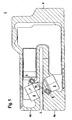
- FIG. 1 schematically shows the structure of a device 1 for detecting applied to a substrate 2 labels 3.
- the device 1 is integrated in a fork-shaped housing 4 with two spaced apart, mutually parallel fork arms 4a, 4b.
- the strip-shaped carrier material 2 with the labels 3 is guided through the intermediate space of the fork arms 4a, 4b, wherein in the present case they are guided resting on the lower fork arm 4a in a detection plane.
- an ultrasonic sensor and an optical sensor are arranged in the housing 4 of the device 1. Via switching means, either the ultrasonic sensor or the optical sensor is activated in order to be able to detect the labels 3 on the carrier material 2 in the detection plane.
- the ultrasonic sensor has an ultrasonic transmitter 5 integrated in the lower fork arm 4a and an ultrasonic receiver 6 arranged in the upper fork arm 4b.
- the ultrasonic transmitter 5 emits directional ultrasonic waves along a beam axis 7, these partially passing through the carrier material 2 and the labels 3 and then guided to the ultrasonic receiver 6.
- the beam axis 7 extends at an inclination angle inclined to the surface normal of the detection plane. As a result of this inclination of the beam axis 7 to the surface of the carrier material 2 with the labels 3 to be detected, interference-related minima and maxima of the ultrasonic waves are also partially averaged out.
- the optical sensor has a transmitter 8 integrated in the lower fork arm 4a and a receiver 9 arranged in the upper fork arm 4b.
- the transmitter 8 emits transmitted light rays along an optical axis 10, wherein the transmitted light beams partially pass through the carrier material 2 with the labels 3 and are then guided to the receiver 9.
- the transmitter 8 emits transmitted light rays in the infrared range.
- the optical axis 10 of the transmitter 8 also extends inclined to the plane of the carrier material 2.
- the arrangement of the ultrasonic sensor and the optical sensor is selected so that the beam axis 7 and the optical axis 10 intersect in the detection plane.
- the arrangement of the optical sensor in the housing 4 may be modified such that mirrors for deflecting the transmitted light beams are used for coupling the transmitted light beams into the detection plane.
- FIG. 2 shows the evaluation circuit 11 for the device 1 according to FIG. 1 ,
- the ultrasonic transmitter 5 and the ultrasonic receiver 6 are shown as components of the ultrasonic sensor and the transmitter 8 and the receiver 9 as components of the optical sensor and with the same reference numerals as in FIG. 1 designated.
- the ultrasonic sensor is driven by a driver circuit consisting of a coil 12, a MOSFET transistor 13 and a resistor 14. With the coil 12, the voltage required for the operation of the ultrasonic transmitter 5 is provided, the MOSFET transistor 13 is used for switching the ultrasonic transmitter 5.
- the optical sensor is driven by a driver circuit consisting of a transistor 15 and two resistors 16, 17.
- a trigger button 18 is actuated by a user, which is attached to the outside of the housing 4 of the device 1.
- the shutter button 18 forms with a resistor 19, the input circuit for a D flip-flop 20.
- the second switch 22 only the ultrasonic receiver 6 or the receiver 9 is connected to the evaluation circuit 11, depending on the control of the D flip-flop 20.
- a light emitting diode 23, 24 is connected in each case.
- the visible on the outside of the housing 4 LEDs form display elements that signal whether the ultrasonic sensor or the optical sensor is activated. In the event that the ultrasonic sensor is activated, only the first light-emitting diode 23 lights up. In the event that the optical sensor is activated, only the second light-emitting diode 24 lights up.
- the ultrasound waves emitted by the ultrasound sensor or the transmitted light beams emitted by the emitter 8 are modulated by the modulation unit 25.
- the modulation unit 25 comprises two pulse generators 26, 27, which in each case a resistor 28, 29 is connected upstream.
- a ramp circuit consisting of resistors 30, 31 and capacitors 32, 33 is provided.
- the outputs of the pulse generators 26, 27 are guided to an AND gate 34, which is connected to the switch 21.
- the ramp circuit generates square-wave pulses with the frequency f 1 .
- the second pulse generator 27 is the rectangular pulses the higher frequency Modulation frequency f 2 superimposed.
- the ultrasound waves or the transmitted light beams this modulation is impressed.
- the received signals of the ultrasonic receiver 6 or receiver 9 are filtered in a circuit consisting of a resistor 35, a bandpass filter 36, a capacitor 37 and two diodes 38a, 38b and then fed to the receiving part of the evaluation circuit 11, which a Evaluation unit 39 forms integrated with matching circuit.
- the evaluation unit 39 has a comparator 40 and a switching output 41 connected thereto. During operation of the device 1, only the ultrasonic sensor or the optical sensor is activated for label detection. To distinguish the labels 3 from the carrier material 2, the received signals of the ultrasonic receiver 6 or the receiver 9 are evaluated in the comparator 40 with a threshold value, whereby a binary switching signal is generated, indicate the switching states, whether a label 3 has been detected or not. This binary switching signal is output via the switching output.
- the threshold value is determined by means of a calibration process, which is carried out before operation of the device 1.
- a calibration process which is carried out before operation of the device 1.
- either the ultrasonic sensor or the optical sensor is activated by performing the trigger button 18 before performing the adjustment process.
- the adjustment process is performed by means of the adjustment circuit.
- the adjustment circuit has a teach-in button 42, with which the adjustment process can be started.
- the threshold value for the comparator 40 is derived automatically from the received signals of the ultrasound receiver 6 or of the receiver 9 registered during label detection.
- the teach-in button 42 is actuated by a user a first time. Then, preferably, the carrier material 2 is automatically guided with the labels 3 through the detection plane. The recorded receive signals are stored in a sample and hold member 43.
- the teach-in key 42 is actuated a second time. This is followed by an automatic adjustment of the threshold value for the comparator 40 to the peak values of the received signals stored in the sample and hold element 43.
- the peak values correspond to the received signals upon detection of the carrier material 2 without labels 3.
- the adjustment circuit comprises a comparator 44 with upstream capacitor 45 and a comparator 44 downstream D-type flip-flop 46.
- an output Q of the D flip-flop 46 includes a trigger circuit with a cut trigger 47 and upstream resistor 48 and capacitor 49 and parallel thereto a step generator 50 on.
- the output Q of the D flip-flop 46 is fed to an input CS of an E 2 potentiometer 51 and to a switch 52.
- the cut trigger 47 is guided on an input U / D of the E 2 potentiometer 51.
- the step generator is routed to another input of the E 2 potentiometer 51.
- the output of the E 2 comparator is fed to an input of the comparator 44.
- the output of the E 2 potentiometer 51 is guided via a divider 53 consisting of two resistors 53 a, 53 b to an input of the comparator 40 used to generate the binary switching signal.
- the E 2 potentiometer 51 is reset via the D flip-flop 46 and the cut trigger 47 to an initial value.
- the switch 52 is closed by actuating the teach-in button 42. Then, the input U / D of the E 2 potentiometer 51 is controlled via the D flip-flop 46 and the cut trigger 47, so that this increases its resistance incrementally. In this case, the increments for increasing the resistance value are predetermined by the step generator 50. The incrementation in the E 2 potentiometer 51 takes place until its output signal corresponds to the peak value of the received signals stored in the sample and hold element 43. Since then the comparator 44 is reversed and this thereby controls the D flip-flop 46 accordingly, the increment of the E 2 potentiometer 51 is terminated thereon. The output signal then present at the output of the E 2 potentiometer 51 then defines the threshold value for the comparator 40 for the operation of the device 1 subsequent to the calibration process.
- the threshold value does not correspond to the peak value of the received signal but a fraction thereof, which is determined by the resistors 53 a, b of the divider 53.
- the resistors of the divider 53 are dimensioned such that the threshold value for the comparator 40 corresponds to half the peak value.
Landscapes
- Geophysics And Detection Of Objects (AREA)
- Labeling Devices (AREA)
Abstract
Description
Die Erfindung betrifft eine Vorrichtung zur Detektion von Etiketten auf einem Trägermaterial.The invention relates to a device for detecting labels on a carrier material.
Eine derartige Vorrichtung ist aus der
Bei dieser Vorrichtung hat sich als nachteilig herausgestellt, dass insbesondere bei dickeren Trägermaterialien, die beispielsweise aus Papier bestehen, eine sichere Detektion von Etiketten nicht gewährleistet ist.In this device has proved to be disadvantageous that, especially with thicker carrier materials, which consist for example of paper, a reliable detection of labels is not guaranteed.
Die
Der Erfindung liegt die Aufgabe zugrunde eine Vorrichtung der eingangs genannten Art bereitzustellen, mittels derer für ein möglichst breites Spektrum von Trägermaterialien und Etikettenmaterialien eine sichere Etikettenerkennung möglich ist.The invention has for its object to provide a device of the type mentioned, by means of which for the broadest possible range of carrier materials and label materials a secure label recognition is possible.
Zur Lösung dieser Aufgabe sind die Merkmale des Anspruchs 1 vorgesehen. Vorteilhafte Ausführungsformen und zweckmäßige Weiterbildungen der Erfindung sind in den Unteransprüchen beschrieben.To solve this problem, the features of
Die erfindungsgemäße Vorrichtung dient zur Detektion von Etiketten auf einem Trägermaterial, und umfasst einen optischen Sensor sowie einen Ultraschallsensor, welche über Schaltmittel wahlweise zur Detektion der Etiketten aktivierbar sind.The device according to the invention serves for the detection of labels on a carrier material, and comprises an optical sensor and an ultrasonic sensor, which can be activated via switching means optionally for the detection of the labels.
Da bei der erfindungsgemäßen Vorrichtung wahlweise ein optischer Sensor oder Ultraschallsensor zur Etikettendetektion eingesetzt werden kann, wird mit dieser eine sichere Etikettendetektion für ein breites Materialspektrum von Etiketten- und Trägermaterialien erreicht.Since either an optical sensor or an ultrasonic sensor for label detection can be used in the device according to the invention, a reliable label detection for a wide range of materials of label and carrier materials is achieved with this.
Während mit dem Ultraschallsensor besonders gut Etiketten auf transparenten, insbesondere schienartigen Trägermaterialien detektiert werden können, eignet sich der optische Sensor insbesondere zur Detektion von Etiketten auf dickeren, nicht transparenten Trägermaterialien wie beispielsweise aus Papier bestehenden Trägermaterialien.While it is particularly easy to detect labels on transparent, in particular bar-like carrier materials with the ultrasonic sensor, the optical sensor is particularly suitable for detecting labels on thick, non-transparent carrier materials such as, for example, paper carrier materials.
Die Auswahl des optischen Sensors zur Etikettendetektion erfolgt durch Betätigung der Schaltmittel und kann so einfach von einem Benutzer durchgeführt werden.The selection of the optical sensor for label detection is carried out by actuation of the switching means and can be carried out so easily by a user.
In einer besonders vorteilhaften Ausführungsform der Erfindung arbeiten sowohl der optische Sensor als auch der Ultraschallsensor nach dem Lichtschrankenprinzip, das heißt der Sender und der Empfänger des optischen Sensors einerseits sowie der Ultraschallsender und der Ultraschallempfänger des Ultraschallsensors andererseits sind jeweils beidseits einer Nachweiseebene, in welcher das Trägermaterial mit den Etiketten relativ zur Vorrichtung geführt wird, angeordnet. Dabei ist die Vorrichtung bevorzugt in einem gabelförmigen Gehäuse mit zwei Gabelarmen, zwischen welchen die Nachweisebene verläuft, angeordnet.In a particularly advantageous embodiment of the invention, both the optical sensor and the ultrasonic sensor work according to the light barrier principle, ie the transmitter and the receiver of the optical sensor on the one hand and the ultrasonic transmitter and the ultrasonic receiver of the ultrasonic sensor on the other hand are each on both sides of a detection plane in which the carrier material with the labels being guided relative to the device, arranged. In this case, the device is preferably arranged in a fork-shaped housing with two fork arms, between which runs the detection plane.
Besonders vorteilhaft sind die Komponenten des optischen Sensors und des Ultraschallsensors so in diesem Gehäuse angeordnet, dass sich die Strahlachse der Ultraschallwellen, die vom Ultraschallsender emittiert werden, und die optische Achse der Sendelichtstrahlen, die vom Sender emittiert werden, in der Nachweisebene schneiden. Damit ist der aktuelle Messort und Messzeitpunkt zur Etikettendetektion unabhängig davon, ob der Ultraschallsensor oder optische Sensor hierfür eingesetzt wird.Particularly advantageously, the components of the optical sensor and the ultrasonic sensor are arranged in this housing so that the beam axis of the ultrasonic waves emitted by the ultrasonic transmitter and the optical axis of the transmitted light beams emitted by the transmitter intersect in the detection plane. Thus, the current location and time of detection for label detection is independent of whether the ultrasonic sensor or optical sensor is used for this purpose.
In einer vorteilhaften Ausführungsform erfolgt die Etikettendetektion durch eine Schwellwertbewertung der Empfangssignale des Empfängers oder des Ultraschallempfänger. Der hierfür verwendete Schwellwert wird bevorzugt in einem Abgleichvorgang bestimmt, wobei während des Abgleichvorgangs das Trägermaterial mit den Etiketten mit dem optischen Sensor oder dem Ultraschallsensor detektiert wird. Da somit der Schwellwert aus den Messwerten der Etikettendetektion selbst abgeleitet wird, wird eine besonders hohe Nachweissicherheit erzielt.In an advantageous embodiment, the label detection is carried out by a threshold value of the received signals of the receiver or the ultrasonic receiver. The threshold value used for this purpose is preferably determined in a calibration process, wherein the carrier material with the labels with the optical sensor or the ultrasonic sensor is detected during the adjustment process. Since the threshold value is thus derived from the measured values of the label detection itself, a particularly high level of detection reliability is achieved.
Ein Vorteil der erfindungsgemäßen Vorrichtung besteht weiterhin darin, dass wesentliche Teile der Auswerteschaltung dieser Vorrichtung sowohl für den optischen Sensor als auch dem Ultraschallsensor genutzt werden können, wodurch sich ein besonders einfacher und damit kostengünstiger Aufbau der Auswerteschaltung ergibt. Insbesondere kann eine Modulationseinheit sowohl zur Modulation der vom Ultraschallsender emittierten Ultraschallwellen als auch zur Modulation der vom Sender emittierten Sendelichtstrahlen genutzt werden. Weiterhin kann eine Abgleichschaltung zur Durchführung eines Abgleichs bei aktiviertem Ultraschallsensor oder bei aktiviertem optischen Sensor verwendet werden.An advantage of the device according to the invention continues to be that essential parts of the evaluation circuit of this device can be used for both the optical sensor and the ultrasonic sensor, resulting in a particularly simple and thus cost-effective design of the evaluation circuit. In particular, a modulation unit can be used both for the modulation of the ultrasonic waves emitted by the ultrasonic transmitter and for the modulation of the transmitted light beams emitted by the transmitter. Furthermore, an adjustment circuit can be used to perform an adjustment when the ultrasonic sensor is activated or when the optical sensor is activated.
Die Erfindung wird im Nachstehenden anhand der Zeichnungen erläutert. Es zeigen:
- Figur 1:
- Ausführungsbeispiel einer Vorrichtung zur Detektion von Etiketten auf einem Trägermaterial.
- Figur 2:
- Auswerteschaltung für die Vorrichtung gemäß
Figur 1
- FIG. 1:
- Embodiment of a device for detecting labels on a carrier material.
- FIG. 2:
- Evaluation circuit for the device according to
FIG. 1 ,
Das bandförmige Trägermaterial 2 mit den Etiketten 3 wird durch den Zwischenraum der Gabelarme 4a, 4b geführt, wobei diese im vorliegenden Fall auf dem unteren Gabelarm 4a aufliegend in einer Nachweisebene geführt sind.The strip-shaped carrier material 2 with the labels 3 is guided through the intermediate space of the
Zur Detektion der Etiketten 3 auf dem Trägermaterial 2 sind im Gehäuse 4 der Vorrichtung 1 ein Ultraschallsensor und ein optischen Sensor angeordnet. Über Schaltmittel wird entweder der Ultraschallsensor oder der optische Sensor aktiviert um die Etiketten 3 auf dem Trägermaterial 2 in der Nachweisebene erfassen zu können.For detecting the labels 3 on the carrier material 2, an ultrasonic sensor and an optical sensor are arranged in the housing 4 of the
Der Ultraschallsensor weist einen im unteren Gabelarm 4a integrierten Ultraschallsender 5 sowie einen im oberen Gabelarm 4b angeordneten Ultraschallempfänger 6 auf. Der Ultraschallsender 5 emittiert gerichtete Ultraschallwellen entlang einer Strahlachse 7, wobei diese das Trägermaterial 2 und die Etiketten 3 teilweise durchsetzen und dann zum Ultraschallempfänger 6 geführt sind. Die Strahlachse 7 verläuft in einem Neigungswinkel geneigt zur Oberflächennormalen der Nachweisebene. Durch diese Neigung der Strahlachse 7 zur Oberfläche des Trägermaterials 2 mit den zu detektierenden Etiketten 3 werden auch Interferenzen bedingte Minima und Maxima der Ultraschallwellen teilweise ausgemittelt.The ultrasonic sensor has an
Der optische Sensor weist einen im unteren Gabelarm 4a integrierten Sender 8 sowie einen im oberen Gabelarm 4b angeordneten Empfänger 9 auf. Der Sender 8 emittiert Sendelichtstrahlen entlang einer optischen Achse 10, wobei die Sendelichtstrahlen das Trägermaterial 2 mit den Etiketten 3 teilweise durchsetzen und dann zum Empfänger 9 geführt werden. Der Sender 8 emittiert Sendelichtstrahlen im Infrarotbereich. Die optische Achse 10 des Senders 8 verläuft ebenfalls geneigt zur Ebene des Trägermaterials 2. Dabei ist die Anordnung des Ultraschallsensors und des optischen Sensors so gewählt, dass sich die Strahlachse 7 und die optische Achse 10 in der Nachweisebene schneiden.The optical sensor has a transmitter 8 integrated in the
Prinzipiell kann die Anordnung des optischen Sensors im Gehäuse 4 derart modifiziert sein, dass zur Einkopplung der Sendelichtstrahlen in die Nachweisebene Spiegel zur Umlenkung der Sendelichtstrahlen eingesetzt werden.In principle, the arrangement of the optical sensor in the housing 4 may be modified such that mirrors for deflecting the transmitted light beams are used for coupling the transmitted light beams into the detection plane.
Der Ultraschallsensor wird mit einer Treiberschaltung bestehend aus einer Spule 12, einem MOSFET-Transistor 13 und einem Widerstand 14 angesteuert. Mit der Spule 12 wird die für den Betrieb des Ultraschallsenders 5 erforderliche Spannung bereitgestellt, der MOSFET-Transistor 13 dient zum Schalten des Ultraschallsenders 5. Der optische Sensor wird mit einer Treiberschaltung bestehend aus einem Transistor 15 und zwei Widerständen 16, 17 angesteuert.The ultrasonic sensor is driven by a driver circuit consisting of a
Über Schaltmittel wird wahlweise der Ultraschallsensor oder der optische Sensor aktiviert. Zur Auswahl des Ultraschallsensors oder des optischen Sensors wird von einem Benutzer eine Auslösetaste 18 betätigt, die an der Außenseite des Gehäuses 4 der Vorrichtung 1 angebracht ist. Die Auslösetaste 18 bildet mit einem Widerstand 19 die Eingangsbeschaltung für ein D-Flipflop 20. Mit dem ersten Schalter 21 wird abhängig von der Ansteuerung des D-Flipflops 20 nur der Ultraschallsender 5 oder der Sender 8 an die Auswerteschaltung 11 angeschlossen. Mit dem zweiten Schalter 22 wird abhängig von der Ansteuerung des D-Flipflops 20 nur der Ultraschallempfänger 6 oder der Empfänger 9 an die Auswerteschaltung 11 angeschlossen.By switching means either the ultrasonic sensor or the optical sensor is activated. To select the ultrasonic sensor or the optical sensor, a
An die Ausgänge Q, Q des D-Flipflops 20 ist jeweils eine Leuchtdiode 23, 24 angeschlossen. Die an der Außenseite des Gehäuses 4 sichtbar angeordneten Leuchtdioden bilden Anzeigeelemente, die signalisieren, ob der Ultraschallsensor oder der optische Sensor aktiviert ist. Für den Fall, dass der Ultraschallsensor aktiviert ist, leuchtet nur die erste Leuchtdiode 23. Für den Fall, dass der optische Sensor aktiviert ist, leuchtet nur die zweite Leuchtdiode 24.To the outputs Q, Q of the D flip-flop 20, a
Wie aus
Die Modulationseinheit 25 umfasst zwei Impulsgeneratoren 26, 27, welchen jeweils ein Widerstand 28, 29 vorgeschaltet ist.The
Zwischen den Impulsgeneratoren 26, 27 ist eine Rampenschaltung bestehend aus Widerständen 30, 31 und Kondensatoren 32, 33 vorgesehen. Die Ausgänge der Impulsgeneratoren 26, 27 sind auf ein UND-Glied 34 geführt, welches an den Schalter 21 angeschlossen ist.Between the
Der erste Impulsgenerator 26 erzeugt Pulse mit einer Frequenz, welche im vorliegenden Fall bei f1 = 9 kHz liegt. Der zweite Impulsgenerator 27 erzeugt Pulse mit einer höheren Frequenz f2, welche im vorliegenden Fall bei f2 = 300 kHz liegt.The
Mit der Rampenschaltung werden Rechteckpulse mit der Frequenz f1 generiert. Durch den zweiten Impulsgenerator 27 ist den Rechteckpulsen die höherfrequente Modulationsfrequenz f2 überlagert. Je nach Schalterstellung des Schalters 21 wird den Ultraschallwellen oder den Sendelichtstrahlen diese Modulation aufgeprägt.The ramp circuit generates square-wave pulses with the frequency f 1 . By the
Je nach Schalterstellung des Schalters 22 werden die Empfangssignale des Ultraschallempfängers 6 oder Empfängers 9 in einer Schaltungsanordnung bestehend aus einem Widerstand 35, einem Bandpassfilter 36, einem Kondensator 37 und zwei Dioden 38a, 38b gefiltert und dann dem empfangsseitigen Teil der Auswerteschaltung 11 zugeführt, welche eine Auswerteeinheit 39 mit darin integrierter Abgleichschaltung bildet.Depending on the switch position of the switch 22, the received signals of the
Die Auswerteeinheit 39 weist einen Komparator 40 und einen an diesen angeschlossenen Schaltausgang 41 auf. Während des Betriebs der Vorrichtung 1 ist zur Etikettendetektion nur der Ultraschallsensor oder der optische Sensor aktiviert. Zur Unterscheidung der Etiketten 3 vom Trägermaterial 2 werden in dem Komparator 40 die Empfangssignale des Ultraschallempfängers 6 oder des Empfängers 9 mit einem Schwellwert bewertet, wodurch ein binäres Schaltsignal generiert wird, dessen Schaltzustände angeben, ob eine Etikette 3 erfasst wurde oder nicht. Dieses binäre Schaltsignal wird über den Schaltausgang ausgegeben.The
Der Schwellwert wird mittels eines Abgleichvorgangs bestimmt, der vor Betrieb der Vorrichtung 1 durchgeführt wird. Dabei wird vor Durchführung des Abgleichvorgangs durch Betätigen der Auslösetaste 18 entweder der Ultraschallsensor oder der optische Sensor aktiviert. Der Abgleichvorgang wird mittels der Abgleichschaltung durchgeführt.The threshold value is determined by means of a calibration process, which is carried out before operation of the
Die Abgleichschaltung weist eine Teach-in Taste 42 auf, mit welcher der Abgleichvorgang gestartet werden kann. Während des Abgleichvorgangs wird der Schwellwert für den Komparator 40 selbsttätig aus den Empfangssignalen des Ultraschallempfängers 6 oder des Empfängers 9, die bei einer Etikettendetektion registriert werden, abgeleitet.The adjustment circuit has a teach-in
Zum Start des Abgleichvorgangs wird die Teach-in Taste 42 durch einen Benutzer ein erstes Mal betätigt. Daraufhin wird vorzugsweise automatisiert das Trägermaterial 2 mit den Etiketten 3 durch die Nachweisebene geführt. Die dabei registrierten Empfangssignale werden in einem Sample- und Hold Glied 43 abgelegt.To start the adjustment process, the teach-in
Danach wird die Teach-in Taste 42 ein zweites Mal betätigt. Daraufhin erfolgt ein selbsttätiger Abgleich des Schwellwerts für den Komparator 40 auf die Spitzenwerte der im Sample- und Hold Glied 43 abgelegten Empfangssignale.Thereafter, the teach-in key 42 is actuated a second time. This is followed by an automatic adjustment of the threshold value for the
Da sowohl die Ultraschallwellen als auch die Sendelichtstrahlen bei Durchgang durch das Trägermaterial 2 und eine Etikette 3 stärker geschwächt werden als bei Durchgang alleine durch das Trägermaterial 2, entsprechen die Spitzenwerte den Empfangssignalen bei Detektion des Trägermaterials 2 ohne Etiketten 3.Since both the ultrasonic waves and the transmitted light beams are weakened more strongly when passing through the carrier material 2 and a label 3 than when passing through the carrier material 2 alone, the peak values correspond to the received signals upon detection of the carrier material 2 without labels 3.
Die Abgleichschaltung umfasst einen Komparator 44 mit vorgeordnetem Kondensator 45 und ein dem Komparator 44 nachgeordnetes D-Flipflop 46. Weiterhin schließt an einen Ausgang Q des D-Flipflops 46 eine Triggerschaltung mit einem Schnitt-Trigger 47 und vorgeordneten Widerstand 48 und Kondensator 49 und parallel hierzu ein Step-Generator 50 an. Der Ausgang Q des D-Flipflops 46 ist auf einem Eingang CS eines E2-Potentiomentors 51 und auf einen Schalter 52 geführt. Der Schnitt-Trigger 47 ist auf einen Eingang U/D des E2-Potentiometers 51 geführt. Der Step-Generator ist auf einen weiteren Eingang des E2-Potentiometers 51 geführt. Der Ausgang des E2-Komparators ist auf einen Eingang des Komparators 44 geführt. Weiterhin ist der Ausgang des E2-Potentiometers 51 über einen Teiler 53 bestehend aus zwei Widerständen 53a, 53b auf einen Eingang des zur Generierung des binären Schaltsignals verwendeten Komparators 40 geführt.The adjustment circuit comprises a
Durch das zweite Betätigen der Teach-in Taste 42 wird das E2-Potentiometer 51 über das D-Flipflop 46 und den Schnitt-Trigger 47 auf einen Ausgangswert zurückgesetzt.By the second actuation of the teach-in
Weiterhin wird durch Betätigen der Teach-in Taste 42 der Schalter 52 geschlossen. Daraufhin wird über das D-Flipflop 46 und den Schnitt-Trigger 47 der Eingang U/D des E2-Potentiometers 51 angesteuert, so dass dieses seinen Widerstandswert inkrementell erhöht. Dabei werden die Inkremente zur Erhöhung des Widerstandswerts durch den Step-Generator 50 vorgegeben. Die Inkrementierung im E2-Potentiometer 51 erfolgt solange, bis dessen Ausgangssignal den im Sample- und Hold Glied 43 gespeicherten Spitzenwert der Empfangssignale entspricht. Da dann der Komparator 44 umgesteuert wird und dieser dadurch das D-Flipflop 46 entsprechend ansteuert, wird darauf die Inkrementierung des E2-Potentiometers 51 beendet. Das dann am Ausgang des E2-Potentiometers 51 anstehende Ausgangssignal definiert dann den Schwellwert für den Komparator 40 für den an den Abgleichvorgang anschließenden Betrieb der Vorrichtung 1.Furthermore, the
Da das Ausgangssignal des E2-Potentiometers 51 nicht direkt sondern über den Teiler 53 dem Eingang des Komparators 40 zugeführt wird, entspricht der Schwellwert nicht dem Spitzenwert des Empfangssignals sondern einem Bruchteil hiervon, welcher durch die Widerstände 53a, b des Teilers 53 bestimmt ist. Im vorliegenden Fall sind die Widerstände des Teilers 53 so dimensioniert, dass der Schwellwert für den Komparator 40 der Hälfte des Spitzenwerts entspricht.Since the output signal of the E 2 potentiometer 51 is supplied not directly but via the
- (1)(1)
- Vorrichtungcontraption
- (2)(2)
- Trägermaterialsupport material
- (3)(3)
- Etiketteetiquette
- (4)(4)
- Gehäusecasing
- (4a, 4b)(4a, 4b)
- Gabelarmefork arms
- (5)(5)
- Ultraschallsenderultrasonic transmitter
- (6)(6)
- Ultraschallempfängerultrasonic receiver
- (7)(7)
- Strahlachsebeam axis
- (8)(8th)
- Sendertransmitter
- (9)(9)
- Empfängerreceiver
- (10)(10)
- optische Achseoptical axis
- (11)(11)
- Auswerteschaltungevaluation
- (12)(12)
- SpuleKitchen sink
- (13)(13)
- MOSFET-TransisterMOSFET Transister
- (14)(14)
- Widerstandresistance
- (15)(15)
- Transistortransistor
- (16)(16)
- Widerstandresistance
- (17)(17)
- Widerstandresistance
- (18)(18)
- Auslösetasterelease button
- (19)(19)
- Widerstandresistance
- (20)(20)
- D-FlipflopD flip-flop
- (21)(21)
- Schalterswitch
- (22)(22)
- Schalterswitch
- (23)(23)
- Leuchtdiodeled
- (24)(24)
- Leuchtdiodeled
- (25)(25)
- Modulationseinheitmodulation unit
- (26)(26)
- Impulsgeneratorpulse generator
- (27)(27)
- Impulsgeneratorpulse generator
- (28)(28)
- Widerstandresistance
- (29)(29)
- Widerstandresistance
- (30)(30)
- Widerstandresistance
- (31)(31)
- Widerstandresistance
- (32)(32)
- Kondensatorcapacitor
- (33)(33)
- Kondensatorcapacitor
- (34)(34)
- UND-GliedAND gate
- (35)(35)
- Widerstandresistance
- (36)(36)
- BandpassfilterBandpass filter
- (37)(37)
- Kondensatorcapacitor
- (38a, b)(38a, b)
- Diodediode
- (39)(39)
- Auswerteinheitevaluation
- (40)(40)
- Komparatorcomparator
- (41)(41)
- Schaltausgangswitching output
- (42)(42)
- Teach-in TasteTeach-in button
- (43)(43)
-
Sample- und Hold Glied 43Sample and hold
member 43 - (44)(44)
- Komparatorcomparator
- (45)(45)
- Kondensatorcapacitor
- (46)(46)
- D-FlipflopD flip-flop
- (47)(47)
- Schnitt-TriggerSchmitt trigger
- (48)(48)
- Widerstandresistance
- (49)(49)
- Kondensatorcapacitor
- (50)(50)
- Step-GeneratorStep generator
- (51)(51)
- E2-PotentiometerE 2 potentiometer
- (52)(52)
- Schalterswitch
- (53)(53)
- Teilerdivider
- (53a, b)(53a, b)
- Widerstandresistance
Claims (11)
- Device for detection of labels (3) on a carrier material (2), characterised in that this comprises an optical sensor (8, 9) and an ultrasonic sensor (5, 6), which are selectably activatible by way of switching means (21 ) for detection of the labels (3).
- Device according to claim 1, characterised in that ultrasonic sensor comprises an ultrasonic transmitter (5), which emits an ultrasonic wave directed longitudinally of a beam axis (7), and an ultrasonic receiver (6), which are arranged on either side of reference plane in which the carrier material (2) with the labels (3) is conveyed.
- Device according to claim 2, characterised in that the optical sensor comprises a transmitter (8), which emits transmitted light beams longitudinally of an optical axis (10), and a receiver (9), which are arranged on either side of the reference plane.
- Device according to claim 3, characterised in that the optical axis (10) of the transmitted light beams and the beam axis (7) of the ultrasonic waves intersect in the reference plane.
- Device according to one of claims 1 to 4, characterised in that this is integrated in a fork-shaped housing (4) with two fork arms (4a, b), which extend parallel to one another at a spacing and between which the reference plane runs.
- Device according to claim 5, characterised in that the ultrasonic transmitter (5) and the transmitter (8) are integrated in a first fork arm (4a) of the housing (4) and the ultrasonic receiver (6) and the receiver (9) are integrated in the second fork arm (4b) of the housing (4).
- Device according to one of claims 1 to 6, characterised in that this comprises a modulation unit (25) for modulation of the ultrasonic waves emitted by the ultrasonic transmitter (5) and the transmitted light beams emitted by the transmitter (8).
- Device according to one of claims 3 to 7, characterised in that for detection of the labels (3) the received signals are evaluated at the output of the ultrasonic receiver (6) or the receiver (9) by a threshold value.
- Device according to claim 8, characterised in that the threshold value is determined during a calibration process.
- Device according to claim 9, characterised in that during the calibration process the carrier material (2) bearing the labels (3) is detected by means of the optical sensor or the ultrasonic sensor and that the threshold value is derived from the received signals then registered at the receiver (9) or ultrasonic receiver (6).
- Device according to claim 10, characterised in that a calibration circuit, to which selectably the received signals of the receiver (9) or of the ultrasonic receiver (6) can be fed, is provided for performance of the calibrating process.
Applications Claiming Priority (1)
| Application Number | Priority Date | Filing Date | Title |
|---|---|---|---|
| DE102005020255 | 2005-04-30 |
Publications (2)
| Publication Number | Publication Date |
|---|---|
| EP1717153A1 EP1717153A1 (en) | 2006-11-02 |
| EP1717153B1 true EP1717153B1 (en) | 2008-08-20 |
Family
ID=36691430
Family Applications (1)
| Application Number | Title | Priority Date | Filing Date |
|---|---|---|---|
| EP06004889A Expired - Lifetime EP1717153B1 (en) | 2005-04-30 | 2006-03-10 | Apparatus for the detection of labels adhering to a backing strip |
Country Status (5)
| Country | Link |
|---|---|
| US (1) | US7437960B2 (en) |
| EP (1) | EP1717153B1 (en) |
| AT (1) | ATE405493T1 (en) |
| DE (1) | DE502006001360D1 (en) |
| ES (1) | ES2308615T3 (en) |
Families Citing this family (4)
| Publication number | Priority date | Publication date | Assignee | Title |
|---|---|---|---|---|
| JP4199741B2 (en) * | 2005-02-25 | 2008-12-17 | Necディスプレイソリューションズ株式会社 | Wave receiver and wave reception determination method |
| DE102005026200A1 (en) | 2005-06-07 | 2006-12-21 | Pepperl + Fuchs Gmbh | Detection and device for the detection of recording media |
| DE102007046769A1 (en) * | 2007-09-29 | 2009-04-16 | Leuze Electronic Gmbh + Co. Kg | sensor arrangement |
| US9239386B2 (en) | 2011-10-05 | 2016-01-19 | Infineon Technologies Ag | Sonic sensors and packages |
Family Cites Families (11)
| Publication number | Priority date | Publication date | Assignee | Title |
|---|---|---|---|---|
| DE8808219U1 (en) * | 1988-06-27 | 1988-08-25 | Eggers Elektronik GmbH, 7530 Pforzheim | Detector for detecting labels on an at least partially transparent, web-shaped carrier |
| US5796091A (en) * | 1993-11-24 | 1998-08-18 | Metrologic Instruments, Inc. | Automatic hand-supportable omnidirectional laser projection scanner with handle-controllable projection axis |
| US5458728A (en) * | 1994-06-27 | 1995-10-17 | Galchefski; John | Apparatus and method for applying labels onto small cylindrical articles with improved seam formation by retarded article rotation |
| US5486063A (en) * | 1995-01-09 | 1996-01-23 | Intermec Incorporated | Method and apparatus for sensing the length of label or tag media by detecting changes in relative thickness |
| JP2000202369A (en) * | 1999-01-12 | 2000-07-25 | Hitachi Ltd | Paper handling equipment |
| DE19927865B4 (en) * | 1999-05-07 | 2005-12-01 | Leuze Electronic Gmbh & Co Kg | Device for detecting objects |
| DE19921217B4 (en) | 1999-05-07 | 2004-11-25 | Leuze Electronic Gmbh + Co Kg | Device for the detection of labels |
| FR2807395A1 (en) * | 2000-04-10 | 2001-10-12 | Vincent Ind | DEROULEUR / ENROULEUR FOR BAND-SUPPORT OF ADHESIVE LABELS OR SIMILAR OBJECTS |
| DE20018193U1 (en) * | 2000-10-25 | 2001-01-04 | Leuze Electronic Gmbh + Co, 73277 Owen | Device for checking sheets |
| EP1348979A1 (en) * | 2002-03-26 | 2003-10-01 | Fuji Photo Film Co., Ltd. | Ultrasonic receiving apparatus and ultrasonic receiving method |
| JP2005162424A (en) * | 2003-12-04 | 2005-06-23 | Nisca Corp | Sheet feeding device and image reading device using this |
-
2006
- 2006-03-10 ES ES06004889T patent/ES2308615T3/en not_active Expired - Lifetime
- 2006-03-10 EP EP06004889A patent/EP1717153B1/en not_active Expired - Lifetime
- 2006-03-10 AT AT06004889T patent/ATE405493T1/en active
- 2006-03-10 DE DE502006001360T patent/DE502006001360D1/en not_active Expired - Lifetime
- 2006-05-01 US US11/415,506 patent/US7437960B2/en not_active Expired - Fee Related
Also Published As
| Publication number | Publication date |
|---|---|
| ES2308615T3 (en) | 2008-12-01 |
| DE502006001360D1 (en) | 2008-10-02 |
| EP1717153A1 (en) | 2006-11-02 |
| US7437960B2 (en) | 2008-10-21 |
| ATE405493T1 (en) | 2008-09-15 |
| US20060260406A1 (en) | 2006-11-23 |
Similar Documents
| Publication | Publication Date | Title |
|---|---|---|
| EP1067053B1 (en) | Device for detecting an object | |
| EP1936400B1 (en) | Laser scanner | |
| EP1435509B1 (en) | Optoelectronic measuring method and device | |
| DE19921217B4 (en) | Device for the detection of labels | |
| CH643961A5 (en) | MONITORING DEVICE ON AN ARRANGEMENT IN WHICH PARTS ARE MOVED. | |
| EP1717153B1 (en) | Apparatus for the detection of labels adhering to a backing strip | |
| DE4323910A1 (en) | Light barrier with evaluation electronics for recognising spurious signals | |
| DE102011081487B4 (en) | Optoelectronic control element and field device for process automation technology with such an optoelectronic control element | |
| CH714486A1 (en) | Sample distribution system and method for distributing samples. | |
| DE202005020654U1 (en) | Device for detection of labels on backing material has optical sensor and ultrasonic sensor activated via switching means for detection of labels | |
| DE202007004364U1 (en) | Sensor arrangement for detecting e.g. label, has guide plates arranged before ultrasonic receiver, where guide plates focusing ultrasonic waves in detection level are provided downstream to ultrasonic transmitter | |
| DE102006041307A1 (en) | Opto-electronic sensor arrangement | |
| DE19806124C1 (en) | Contactless sensor for label scanner | |
| DE19707418C2 (en) | Optoelectronic device | |
| EP1498747A1 (en) | Optoelectronic device | |
| DE102012102056B4 (en) | Optical sensor | |
| EP2535743B1 (en) | Optical sensor | |
| EP3705914B1 (en) | Sensor arrangement | |
| DE2411723A1 (en) | Flaw detector for bottle rims - has laser beam directed by rotating element, housing mirror and photoelectric cell | |
| DE102014111952A1 (en) | Sensor device for detecting an environment of a motor vehicle, driver assistance system, motor vehicle and method | |
| DE4441245A1 (en) | Apparatus for checking presence of label on bottle or similar | |
| DE4132973C2 (en) | Procedure for checking readers | |
| DE10341436B4 (en) | Sensor for detecting transparent object structures | |
| DE10239222A1 (en) | Regulating output intensity of light emitter in light barrier or optical detector, by checking termination criterion if test light signal can be processed at receiver, and changing light intensity if criterion is not fulfilled | |
| DE102005051128B4 (en) | Optical sensor |
Legal Events
| Date | Code | Title | Description |
|---|---|---|---|
| PUAI | Public reference made under article 153(3) epc to a published international application that has entered the european phase |
Free format text: ORIGINAL CODE: 0009012 |
|
| 17P | Request for examination filed |
Effective date: 20060816 |
|
| AK | Designated contracting states |
Kind code of ref document: A1 Designated state(s): AT BE BG CH CY CZ DE DK EE ES FI FR GB GR HU IE IS IT LI LT LU LV MC NL PL PT RO SE SI SK TR |
|
| AX | Request for extension of the european patent |
Extension state: AL BA HR MK YU |
|
| 17Q | First examination report despatched |
Effective date: 20070116 |
|
| AKX | Designation fees paid |
Designated state(s): AT BE BG CH CY CZ DE DK EE ES FI FR GB GR HU IE IS IT LI LT LU LV MC NL PL PT RO SE SI SK TR |
|
| GRAP | Despatch of communication of intention to grant a patent |
Free format text: ORIGINAL CODE: EPIDOSNIGR1 |
|
| GRAS | Grant fee paid |
Free format text: ORIGINAL CODE: EPIDOSNIGR3 |
|
| GRAA | (expected) grant |
Free format text: ORIGINAL CODE: 0009210 |
|
| AK | Designated contracting states |
Kind code of ref document: B1 Designated state(s): AT BE BG CH CY CZ DE DK EE ES FI FR GB GR HU IE IS IT LI LT LU LV MC NL PL PT RO SE SI SK TR |
|
| REG | Reference to a national code |
Ref country code: GB Ref legal event code: FG4D Free format text: NOT ENGLISH |
|
| REG | Reference to a national code |
Ref country code: CH Ref legal event code: EP Ref country code: CH Ref legal event code: NV Representative=s name: ROTTMANN, ZIMMERMANN + PARTNER AG |
|
| REG | Reference to a national code |
Ref country code: IE Ref legal event code: FG4D Free format text: LANGUAGE OF EP DOCUMENT: GERMAN |
|
| REF | Corresponds to: |
Ref document number: 502006001360 Country of ref document: DE Date of ref document: 20081002 Kind code of ref document: P |
|
| REG | Reference to a national code |
Ref country code: ES Ref legal event code: FG2A Ref document number: 2308615 Country of ref document: ES Kind code of ref document: T3 |
|
| PG25 | Lapsed in a contracting state [announced via postgrant information from national office to epo] |
Ref country code: NL Free format text: LAPSE BECAUSE OF FAILURE TO SUBMIT A TRANSLATION OF THE DESCRIPTION OR TO PAY THE FEE WITHIN THE PRESCRIBED TIME-LIMIT Effective date: 20080820 Ref country code: IS Free format text: LAPSE BECAUSE OF FAILURE TO SUBMIT A TRANSLATION OF THE DESCRIPTION OR TO PAY THE FEE WITHIN THE PRESCRIBED TIME-LIMIT Effective date: 20081220 Ref country code: LT Free format text: LAPSE BECAUSE OF FAILURE TO SUBMIT A TRANSLATION OF THE DESCRIPTION OR TO PAY THE FEE WITHIN THE PRESCRIBED TIME-LIMIT Effective date: 20080820 |
|
| PG25 | Lapsed in a contracting state [announced via postgrant information from national office to epo] |
Ref country code: LV Free format text: LAPSE BECAUSE OF FAILURE TO SUBMIT A TRANSLATION OF THE DESCRIPTION OR TO PAY THE FEE WITHIN THE PRESCRIBED TIME-LIMIT Effective date: 20080820 Ref country code: SI Free format text: LAPSE BECAUSE OF FAILURE TO SUBMIT A TRANSLATION OF THE DESCRIPTION OR TO PAY THE FEE WITHIN THE PRESCRIBED TIME-LIMIT Effective date: 20080820 Ref country code: FI Free format text: LAPSE BECAUSE OF FAILURE TO SUBMIT A TRANSLATION OF THE DESCRIPTION OR TO PAY THE FEE WITHIN THE PRESCRIBED TIME-LIMIT Effective date: 20080820 |
|
| REG | Reference to a national code |
Ref country code: IE Ref legal event code: FD4D |
|
| PG25 | Lapsed in a contracting state [announced via postgrant information from national office to epo] |
Ref country code: IE Free format text: LAPSE BECAUSE OF FAILURE TO SUBMIT A TRANSLATION OF THE DESCRIPTION OR TO PAY THE FEE WITHIN THE PRESCRIBED TIME-LIMIT Effective date: 20080820 Ref country code: BG Free format text: LAPSE BECAUSE OF FAILURE TO SUBMIT A TRANSLATION OF THE DESCRIPTION OR TO PAY THE FEE WITHIN THE PRESCRIBED TIME-LIMIT Effective date: 20081120 Ref country code: DK Free format text: LAPSE BECAUSE OF FAILURE TO SUBMIT A TRANSLATION OF THE DESCRIPTION OR TO PAY THE FEE WITHIN THE PRESCRIBED TIME-LIMIT Effective date: 20080820 |
|
| PG25 | Lapsed in a contracting state [announced via postgrant information from national office to epo] |
Ref country code: PT Free format text: LAPSE BECAUSE OF FAILURE TO SUBMIT A TRANSLATION OF THE DESCRIPTION OR TO PAY THE FEE WITHIN THE PRESCRIBED TIME-LIMIT Effective date: 20090120 Ref country code: CZ Free format text: LAPSE BECAUSE OF FAILURE TO SUBMIT A TRANSLATION OF THE DESCRIPTION OR TO PAY THE FEE WITHIN THE PRESCRIBED TIME-LIMIT Effective date: 20080820 Ref country code: RO Free format text: LAPSE BECAUSE OF FAILURE TO SUBMIT A TRANSLATION OF THE DESCRIPTION OR TO PAY THE FEE WITHIN THE PRESCRIBED TIME-LIMIT Effective date: 20080820 Ref country code: SK Free format text: LAPSE BECAUSE OF FAILURE TO SUBMIT A TRANSLATION OF THE DESCRIPTION OR TO PAY THE FEE WITHIN THE PRESCRIBED TIME-LIMIT Effective date: 20080820 |
|
| PLBE | No opposition filed within time limit |
Free format text: ORIGINAL CODE: 0009261 |
|
| STAA | Information on the status of an ep patent application or granted ep patent |
Free format text: STATUS: NO OPPOSITION FILED WITHIN TIME LIMIT |
|
| 26N | No opposition filed |
Effective date: 20090525 |
|
| PG25 | Lapsed in a contracting state [announced via postgrant information from national office to epo] |
Ref country code: EE Free format text: LAPSE BECAUSE OF FAILURE TO SUBMIT A TRANSLATION OF THE DESCRIPTION OR TO PAY THE FEE WITHIN THE PRESCRIBED TIME-LIMIT Effective date: 20080820 |
|
| BERE | Be: lapsed |
Owner name: LEUZE ELECTRONIC G.M.B.H. + CO. KG Effective date: 20090331 |
|
| PG25 | Lapsed in a contracting state [announced via postgrant information from national office to epo] |
Ref country code: MC Free format text: LAPSE BECAUSE OF NON-PAYMENT OF DUE FEES Effective date: 20090331 |
|
| PG25 | Lapsed in a contracting state [announced via postgrant information from national office to epo] |
Ref country code: SE Free format text: LAPSE BECAUSE OF FAILURE TO SUBMIT A TRANSLATION OF THE DESCRIPTION OR TO PAY THE FEE WITHIN THE PRESCRIBED TIME-LIMIT Effective date: 20081120 |
|
| PG25 | Lapsed in a contracting state [announced via postgrant information from national office to epo] |
Ref country code: BE Free format text: LAPSE BECAUSE OF NON-PAYMENT OF DUE FEES Effective date: 20090331 |
|
| PG25 | Lapsed in a contracting state [announced via postgrant information from national office to epo] |
Ref country code: PL Free format text: LAPSE BECAUSE OF FAILURE TO SUBMIT A TRANSLATION OF THE DESCRIPTION OR TO PAY THE FEE WITHIN THE PRESCRIBED TIME-LIMIT Effective date: 20080820 |
|
| PG25 | Lapsed in a contracting state [announced via postgrant information from national office to epo] |
Ref country code: GR Free format text: LAPSE BECAUSE OF FAILURE TO SUBMIT A TRANSLATION OF THE DESCRIPTION OR TO PAY THE FEE WITHIN THE PRESCRIBED TIME-LIMIT Effective date: 20081121 |
|
| PG25 | Lapsed in a contracting state [announced via postgrant information from national office to epo] |
Ref country code: LU Free format text: LAPSE BECAUSE OF NON-PAYMENT OF DUE FEES Effective date: 20090310 |
|
| PG25 | Lapsed in a contracting state [announced via postgrant information from national office to epo] |
Ref country code: HU Free format text: LAPSE BECAUSE OF FAILURE TO SUBMIT A TRANSLATION OF THE DESCRIPTION OR TO PAY THE FEE WITHIN THE PRESCRIBED TIME-LIMIT Effective date: 20090221 |
|
| PG25 | Lapsed in a contracting state [announced via postgrant information from national office to epo] |
Ref country code: TR Free format text: LAPSE BECAUSE OF FAILURE TO SUBMIT A TRANSLATION OF THE DESCRIPTION OR TO PAY THE FEE WITHIN THE PRESCRIBED TIME-LIMIT Effective date: 20080820 |
|
| REG | Reference to a national code |
Ref country code: CH Ref legal event code: PFA Owner name: LEUZE ELECTRONIC GMBH + CO. KG Free format text: LEUZE ELECTRONIC GMBH + CO. KG#IN DER BRAIKE 1#73277 OWEN/TECK (DE) -TRANSFER TO- LEUZE ELECTRONIC GMBH + CO. KG#IN DER BRAIKE 1#73277 OWEN/TECK (DE) |
|
| PG25 | Lapsed in a contracting state [announced via postgrant information from national office to epo] |
Ref country code: CY Free format text: LAPSE BECAUSE OF FAILURE TO SUBMIT A TRANSLATION OF THE DESCRIPTION OR TO PAY THE FEE WITHIN THE PRESCRIBED TIME-LIMIT Effective date: 20080820 |
|
| PGFP | Annual fee paid to national office [announced via postgrant information from national office to epo] |
Ref country code: IT Payment date: 20120326 Year of fee payment: 7 |
|
| PGFP | Annual fee paid to national office [announced via postgrant information from national office to epo] |
Ref country code: FR Payment date: 20130408 Year of fee payment: 8 Ref country code: ES Payment date: 20130326 Year of fee payment: 8 Ref country code: GB Payment date: 20130321 Year of fee payment: 8 Ref country code: CH Payment date: 20130322 Year of fee payment: 8 |
|
| PGFP | Annual fee paid to national office [announced via postgrant information from national office to epo] |
Ref country code: AT Payment date: 20130313 Year of fee payment: 8 |
|
| PGFP | Annual fee paid to national office [announced via postgrant information from national office to epo] |
Ref country code: DE Payment date: 20130413 Year of fee payment: 8 |
|
| REG | Reference to a national code |
Ref country code: DE Ref legal event code: R119 Ref document number: 502006001360 Country of ref document: DE |
|
| REG | Reference to a national code |
Ref country code: CH Ref legal event code: PL |
|
| REG | Reference to a national code |
Ref country code: AT Ref legal event code: MM01 Ref document number: 405493 Country of ref document: AT Kind code of ref document: T Effective date: 20140310 |
|
| GBPC | Gb: european patent ceased through non-payment of renewal fee |
Effective date: 20140310 |
|
| REG | Reference to a national code |
Ref country code: FR Ref legal event code: ST Effective date: 20141128 |
|
| REG | Reference to a national code |
Ref country code: DE Ref legal event code: R119 Ref document number: 502006001360 Country of ref document: DE Effective date: 20141001 |
|
| PG25 | Lapsed in a contracting state [announced via postgrant information from national office to epo] |
Ref country code: FR Free format text: LAPSE BECAUSE OF NON-PAYMENT OF DUE FEES Effective date: 20140331 Ref country code: CH Free format text: LAPSE BECAUSE OF NON-PAYMENT OF DUE FEES Effective date: 20140331 Ref country code: GB Free format text: LAPSE BECAUSE OF NON-PAYMENT OF DUE FEES Effective date: 20140310 Ref country code: DE Free format text: LAPSE BECAUSE OF NON-PAYMENT OF DUE FEES Effective date: 20141001 Ref country code: LI Free format text: LAPSE BECAUSE OF NON-PAYMENT OF DUE FEES Effective date: 20140331 |
|
| PG25 | Lapsed in a contracting state [announced via postgrant information from national office to epo] |
Ref country code: AT Free format text: LAPSE BECAUSE OF NON-PAYMENT OF DUE FEES Effective date: 20140310 |
|
| PG25 | Lapsed in a contracting state [announced via postgrant information from national office to epo] |
Ref country code: IT Free format text: LAPSE BECAUSE OF NON-PAYMENT OF DUE FEES Effective date: 20140310 |
|
| REG | Reference to a national code |
Ref country code: ES Ref legal event code: FD2A Effective date: 20150828 |
|
| PG25 | Lapsed in a contracting state [announced via postgrant information from national office to epo] |
Ref country code: ES Free format text: LAPSE BECAUSE OF NON-PAYMENT OF DUE FEES Effective date: 20140311 |