EP1712996A1 - Procédé et système de configuration des registres de microcontrôleur, microcontrôleur et produit de logiciel correspondant - Google Patents
Procédé et système de configuration des registres de microcontrôleur, microcontrôleur et produit de logiciel correspondant Download PDFInfo
- Publication number
- EP1712996A1 EP1712996A1 EP05425233A EP05425233A EP1712996A1 EP 1712996 A1 EP1712996 A1 EP 1712996A1 EP 05425233 A EP05425233 A EP 05425233A EP 05425233 A EP05425233 A EP 05425233A EP 1712996 A1 EP1712996 A1 EP 1712996A1
- Authority
- EP
- European Patent Office
- Prior art keywords
- register
- datum
- registers
- respective data
- state
- Prior art date
- Legal status (The legal status is an assumption and is not a legal conclusion. Google has not performed a legal analysis and makes no representation as to the accuracy of the status listed.)
- Withdrawn
Links
Images

Classifications
-
- G—PHYSICS
- G06—COMPUTING; CALCULATING OR COUNTING
- G06F—ELECTRIC DIGITAL DATA PROCESSING
- G06F11/00—Error detection; Error correction; Monitoring
- G06F11/07—Responding to the occurrence of a fault, e.g. fault tolerance
- G06F11/16—Error detection or correction of the data by redundancy in hardware
- G06F11/1666—Error detection or correction of the data by redundancy in hardware where the redundant component is memory or memory area
- G06F11/167—Error detection by comparing the memory output
Definitions
- the present invention relates to techniques for configuring registers, such as memory registers, of microcontrollers, and has been developed with particular attention paid to its possible application in systems affected by the presence of electromagnetic disturbance.
- Electromagnetic disturbance can alter the contents of the registers present within microcontrollers, in this way jeopardizing correct operation of the devices themselves.
- the registers of a microcontroller are typically connected to a single bus, travelling on which are the information data for a particular register or again values of transition between one given item of information and the next.
- the microcontroller selects at a given instant the particular register in which the contents present on the bus are to be written, setting a latch signal for the particular register selected at the logic value "one".
- a typical method for protecting the "critical" values necessary for a correct configuration of the devices envisages that these values will be stored in memory registers of a ROM (Read-Only Memory). Said solution presents the drawback that the values stored cannot be modified and personalized on the basis of the type of application and of the specific requirements of the user.
- the fuse structures comprise fuse devices, which, if traversed by a current, enable connection of a particular node of the circuit to the supply voltage or else to ground. In this way, the definitive configuration of the microcontroller is determined.
- the option bytes which are constituted by a nonvolatile-memory region typically present in a microcontroller, the bits of which are accessible directly by the microcontroller, present the advantage, as compared to the fuse structures, of being modifiable a number of times (just in the programming step and not during run-time operation) but call for a high number of direct connections between the microcontroller and the memory.
- the object of present invention is to satisfy the aforesaid need.
- the present invention also relates to a corresponding system, as well as a microcontroller equipped with said system, and a computer-program product, which can be loaded into the memory of at least one computer and comprises portions of software code for implementing the aforesaid method.
- computer-program product is intended to refer to a computer-readable medium containing instructions for controlling a computer system for co-ordinating execution of the method of the invention.
- Reference to "at least one computer” is evidently intended to highlight the possibility for the method according to the present invention to be implemented in a distributed and/or modular fashion.
- the solution described herein enables the values contained in the option bytes of the nonvolatile memory to be written in some flip-flop registers upon start-up of the device, reading one byte at a time, and hence without the need to use dedicated connections, and with the purpose of verifying in run time any possible corruption of said registers and of restoring, in that case, the correct value.
- microcontroller As a terminological premise of a general nature, it is emphasized that the term “microcontroller” is used herein without setting any specific emphasis on its acceptation as an on-chip computer optimized for controlling devices and equipped with the necessary memories and input/output devices. For the purposes of definition of the scope of the invention, the term “microcontroller” must herein be considered as also comprising e.g. the devices referred to as “microprocessors” or “microcomputers”.
- FIG. 1 illustrates the general structure of a part of a microcontroller comprising a set of registers (for example, two registers 20 and 30) connected, via a bus 70, to a memory 80. Travelling on the bus 70 are the information data for a particular register or again values of transition between one given item of information and the next.
- a set of registers for example, two registers 20 and 30
- Travelling on the bus 70 are the information data for a particular register or again values of transition between one given item of information and the next.
- Operation of the microcontroller envisages that at a given instant the particular register on which the contents present on the bus 70 are to be written is chosen, setting a latch signal for the particular register selected at the logic value "one".
- electromagnetic disturbance can cause the value of a latch signal to exceed a critical threshold and to be recognized as logic "one".
- the value present at that moment on the bus is stored, with a consequent loss of the correct contents of the register.
- EPROM Erasable Programmable Read-Only Memory
- option bytes are formed by a nonvolatile-memory region in which particular configurations of the microcontroller are contained.
- the solution described herein envisages the presence, for each option byte, of its complement in the subsequent nonvolatile-memory location.
- a generic option byte and its negation are read during the start-up step from the memory 80 and made available on the bus 70 for being stored in the two registers 20, 30.
- the value of the option byte is stored in the first register 20 following upon enabling of a latch signal on a line 25; next, the value of the complement of the option byte is stored in the second register 30, once again following upon enabling of a latch signal on a line 35.
- a comparator 10 is connected to the register 20 and to an inverter 50, which is in turn connected to the register 30.
- the comparator 10 is thus able to verify whether the contents of the first register 20 and the logic complement of the contents of the second register 30 (i.e., "the complement of the complement", obtained by means of the inverter 50) are identical to one another.
- the comparator 10 detects the difference and generates an internal reset signal on a line 60, which causes re-reading of the data from the memory 80 and re-writing thereof in the registers 20, 30.
- the above solution presents the advantage of enabling the values stored during the start-up step to be modified a number of times.
- the solution described herein envisages the use of flip-flop registers for providing the registers 20 and 30. These are completely reconfigurable by the user, not only during start-up, but also during normal operation of the device.
- the solution proposed herein hence enables storage of the information data read from the nonvolatile memory during start-up of the device in the flip-flop registers and envisages a technique of recognition of the corruption of the values in the registers and restoration of the correct values.
- the technique of recognition of corruption of the values uses the comparator 10, which is provided with an enable input driven, via a line 90, by a final-state machine 40.
- the final-state machine 40 causes enabling of the comparator 10 only at the end of the operation of writing of the complement of the option byte in the second flip-flop register 30.
- the final-state machine 40 comes into play not only in the step of loading of the generic option byte and of its negation but also when the configuration of the device is to be modified in run time changing the value of a generic option byte.
- the reset signal on the line 60 is disabled for the period strictly necessary for modification of the two registers 20, 30 because, between writing in the first register 20 and writing in the second register 30, the comparator 10 detects a difference between the values in the two registers that is not due to corruption and hence must be masked.
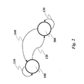
- Figure 2 shows the state diagram of the final-state machine of Figure 1.
- the initial state of the final-state machine 40 is the state "Enabled” 100 and in this state the comparator 10 is always enabled.
- the arrow 110 indicates the permanence of the final-state machine in the state "Enabled” 100.
- a command 120 for writing of the option byte in the first register 20 causes transition of the final-state machine to the state "Disabled” 200, in which the comparator 10 is disabled.
- a count 130 starts, which must be configured on the basis of the characteristics of the microprocessor used, and which maintains the comparator disabled for the time necessary for writing in the second register 30.
- a time-out 140 is triggered, which brings the final-state machine back into the state "Enabled” 100, which re-enables the comparator 10.
- the final-state machine has been devised to be immune to disturbance (noise); in fact, it is only formed by two states and a counter.
- the count value can be altered, but this simply renders the counting step faster and anticipates exit from the disabled state.
- the solution proposed hence enables a configurability of the microcontroller to be provided without any limitations and with a good immunity to electromagnetic noise, further providing the user with the possibility of changing in run time the configuration of the device.
Priority Applications (2)
| Application Number | Priority Date | Filing Date | Title |
|---|---|---|---|
| EP05425233A EP1712996A1 (fr) | 2005-04-15 | 2005-04-15 | Procédé et système de configuration des registres de microcontrôleur, microcontrôleur et produit de logiciel correspondant |
| US11/301,372 US7571379B2 (en) | 2005-04-15 | 2005-12-12 | Method and system for configuring registers in microcontrollers, and corresponding computer-program product |
Applications Claiming Priority (1)
| Application Number | Priority Date | Filing Date | Title |
|---|---|---|---|
| EP05425233A EP1712996A1 (fr) | 2005-04-15 | 2005-04-15 | Procédé et système de configuration des registres de microcontrôleur, microcontrôleur et produit de logiciel correspondant |
Publications (1)
| Publication Number | Publication Date |
|---|---|
| EP1712996A1 true EP1712996A1 (fr) | 2006-10-18 |
Family
ID=34943154
Family Applications (1)
| Application Number | Title | Priority Date | Filing Date |
|---|---|---|---|
| EP05425233A Withdrawn EP1712996A1 (fr) | 2005-04-15 | 2005-04-15 | Procédé et système de configuration des registres de microcontrôleur, microcontrôleur et produit de logiciel correspondant |
Country Status (2)
| Country | Link |
|---|---|
| US (1) | US7571379B2 (fr) |
| EP (1) | EP1712996A1 (fr) |
Citations (5)
| Publication number | Priority date | Publication date | Assignee | Title |
|---|---|---|---|---|
| DE3312873A1 (de) * | 1983-04-11 | 1984-10-25 | Deutsche Fernsprecher Gesellschaft Mbh Marburg, 3550 Marburg | Verfahren zur datensicherung in speichern |
| US5699509A (en) * | 1995-06-07 | 1997-12-16 | Abbott Laboratories | Method and system for using inverted data to detect corrupt data |
| US6201997B1 (en) * | 1995-08-10 | 2001-03-13 | Itt Manufacturing Enterprises, Inc. | Microprocessor system for safety-critical control systems |
| US6230058B1 (en) * | 1998-10-19 | 2001-05-08 | Ela Medical S.A. | Active medical device having protected memory registers for storing adjustable parameter values |
| DE10113319A1 (de) * | 2001-03-20 | 2002-09-26 | Conti Temic Microelectronic | Verfahren zum Betrieb eines von einem Prozessor gesteuerten Systems |
Family Cites Families (3)
| Publication number | Priority date | Publication date | Assignee | Title |
|---|---|---|---|---|
| AU568977B2 (en) * | 1985-05-10 | 1988-01-14 | Tandem Computers Inc. | Dual processor error detection system |
| JP3253296B2 (ja) * | 1989-12-20 | 2002-02-04 | セイコーエプソン株式会社 | 記憶装置及びデータ処理装置 |
| US5894487A (en) * | 1997-07-15 | 1999-04-13 | International Business Machines Corporation | Error detection of directory arrays in dynamic circuits |
-
2005
- 2005-04-15 EP EP05425233A patent/EP1712996A1/fr not_active Withdrawn
- 2005-12-12 US US11/301,372 patent/US7571379B2/en active Active
Patent Citations (5)
| Publication number | Priority date | Publication date | Assignee | Title |
|---|---|---|---|---|
| DE3312873A1 (de) * | 1983-04-11 | 1984-10-25 | Deutsche Fernsprecher Gesellschaft Mbh Marburg, 3550 Marburg | Verfahren zur datensicherung in speichern |
| US5699509A (en) * | 1995-06-07 | 1997-12-16 | Abbott Laboratories | Method and system for using inverted data to detect corrupt data |
| US6201997B1 (en) * | 1995-08-10 | 2001-03-13 | Itt Manufacturing Enterprises, Inc. | Microprocessor system for safety-critical control systems |
| US6230058B1 (en) * | 1998-10-19 | 2001-05-08 | Ela Medical S.A. | Active medical device having protected memory registers for storing adjustable parameter values |
| DE10113319A1 (de) * | 2001-03-20 | 2002-09-26 | Conti Temic Microelectronic | Verfahren zum Betrieb eines von einem Prozessor gesteuerten Systems |
Non-Patent Citations (1)
| Title |
|---|
| ST MICROELECTRONIC: "Datasheet: 8-BIT INTELLIGENT CONTROLLER UNIT (ICU) Rev. 2.3", INET, May 2004 (2004-05-01), XP002344784, Retrieved from the Internet <URL:http://www.st.com/stonline/products/literature/ds/8793.pdf> [retrieved on 20050914] * |
Also Published As
| Publication number | Publication date |
|---|---|
| US20060236173A1 (en) | 2006-10-19 |
| US7571379B2 (en) | 2009-08-04 |
Similar Documents
| Publication | Publication Date | Title |
|---|---|---|
| US4388695A (en) | Hardware memory write lock circuit | |
| JP5535547B2 (ja) | セキュアメモリインターフェース | |
| CN101243451B (zh) | 保护嵌入式存储器的访问的方法和装置 | |
| US8176281B2 (en) | Controlling access to an embedded memory of a microcontroller | |
| US7496738B2 (en) | Method of automatic control of the execution of a program by a microprocessor | |
| JPS63133238A (ja) | デジタルデータ処理システム | |
| JPH063586B2 (ja) | 計算モジュールの監視方法 | |
| US5682496A (en) | Filtered serial event controlled command port for memory | |
| US5740360A (en) | Apparatus and method for resetting a microprocessor in the event of improper program execution | |
| US4875156A (en) | Computer having a protection device to selectively block incorrect control signals | |
| RU2249247C2 (ru) | Защита ядра вычислительного устройства от несанкционированных изменений извне | |
| US7571379B2 (en) | Method and system for configuring registers in microcontrollers, and corresponding computer-program product | |
| US5047982A (en) | Write protection method and apparatus for an EEPROM | |
| US8819449B2 (en) | Event counter in a system adapted to the JavaCard language | |
| WO2001097010A2 (fr) | Procede et dispositif de traitement de donnees servant a proteger l'execution d'instructions | |
| US5057999A (en) | Microprocessor having a protection circuit to insure proper instruction fetching | |
| US6813191B2 (en) | Microcomputer with nonvolatile memory protected against false erasing or writing | |
| US11188656B2 (en) | Secure software system for microcontroller or the like and method therefor | |
| US7246206B2 (en) | Method and device for storing a computer program in a program memory of a control unit | |
| JP3114645B2 (ja) | メモリセル装置のリセット制御回路 | |
| RU2265240C2 (ru) | Модуль системного контроля | |
| CN111314045B (zh) | 识别激光故障注入攻击的方法、装置、存储介质及终端 | |
| JP2002099468A (ja) | 書き込み制御回路 | |
| JP2001014872A (ja) | 不揮発性半導体メモリ誤書き込み防止方式 | |
| JPH08273346A (ja) | 集積メモリ回路の書込保護方法及び対応する集積メモリ回路 |
Legal Events
| Date | Code | Title | Description |
|---|---|---|---|
| PUAI | Public reference made under article 153(3) epc to a published international application that has entered the european phase |
Free format text: ORIGINAL CODE: 0009012 |
|
| AK | Designated contracting states |
Kind code of ref document: A1 Designated state(s): AT BE BG CH CY CZ DE DK EE ES FI FR GB GR HU IE IS IT LI LT LU MC NL PL PT RO SE SI SK TR |
|
| AX | Request for extension of the european patent |
Extension state: AL BA HR LV MK YU |
|
| 17P | Request for examination filed |
Effective date: 20070223 |
|
| 17Q | First examination report despatched |
Effective date: 20070322 |
|
| 17Q | First examination report despatched |
Effective date: 20070322 |
|
| AKX | Designation fees paid |
Designated state(s): DE FR GB IT |
|
| STAA | Information on the status of an ep patent application or granted ep patent |
Free format text: STATUS: THE APPLICATION IS DEEMED TO BE WITHDRAWN |
|
| 18D | Application deemed to be withdrawn |
Effective date: 20071002 |