EP1712937A2 - Optical curved directional coupler and method - Google Patents
Optical curved directional coupler and method Download PDFInfo
- Publication number
- EP1712937A2 EP1712937A2 EP06251058A EP06251058A EP1712937A2 EP 1712937 A2 EP1712937 A2 EP 1712937A2 EP 06251058 A EP06251058 A EP 06251058A EP 06251058 A EP06251058 A EP 06251058A EP 1712937 A2 EP1712937 A2 EP 1712937A2
- Authority
- EP
- European Patent Office
- Prior art keywords
- coupler
- waveguide
- waveguides
- splitting ratio
- plc
- Prior art date
- Legal status (The legal status is an assumption and is not a legal conclusion. Google has not performed a legal analysis and makes no representation as to the accuracy of the status listed.)
- Withdrawn
Links
Images

Classifications
-
- G—PHYSICS
- G02—OPTICS
- G02B—OPTICAL ELEMENTS, SYSTEMS OR APPARATUS
- G02B6/00—Light guides; Structural details of arrangements comprising light guides and other optical elements, e.g. couplings
- G02B6/10—Light guides; Structural details of arrangements comprising light guides and other optical elements, e.g. couplings of the optical waveguide type
- G02B6/12—Light guides; Structural details of arrangements comprising light guides and other optical elements, e.g. couplings of the optical waveguide type of the integrated circuit kind
- G02B6/12007—Light guides; Structural details of arrangements comprising light guides and other optical elements, e.g. couplings of the optical waveguide type of the integrated circuit kind forming wavelength selective elements, e.g. multiplexer, demultiplexer
-
- G—PHYSICS
- G02—OPTICS
- G02B—OPTICAL ELEMENTS, SYSTEMS OR APPARATUS
- G02B6/00—Light guides; Structural details of arrangements comprising light guides and other optical elements, e.g. couplings
- G02B6/10—Light guides; Structural details of arrangements comprising light guides and other optical elements, e.g. couplings of the optical waveguide type
- G02B6/12—Light guides; Structural details of arrangements comprising light guides and other optical elements, e.g. couplings of the optical waveguide type of the integrated circuit kind
- G02B6/122—Basic optical elements, e.g. light-guiding paths
- G02B6/125—Bends, branchings or intersections
-
- G—PHYSICS
- G02—OPTICS
- G02B—OPTICAL ELEMENTS, SYSTEMS OR APPARATUS
- G02B6/00—Light guides; Structural details of arrangements comprising light guides and other optical elements, e.g. couplings
- G02B6/10—Light guides; Structural details of arrangements comprising light guides and other optical elements, e.g. couplings of the optical waveguide type
- G02B6/12—Light guides; Structural details of arrangements comprising light guides and other optical elements, e.g. couplings of the optical waveguide type of the integrated circuit kind
- G02B2006/12133—Functions
- G02B2006/12147—Coupler
Definitions
- the width (w 1 ) of the first waveguide 110 and the width (w 2 ) of the second waveguide 120 are preferably selected to be about the minimum mode width (i.e. the point at which the fundamental mode in the waveguide has a minimum width). Such a minimum mode width provides improved insensitivity to waveguide width changes.
- Formulae for calculating R c (and accordingly R c1 and R c2 ) and L c can be derived, provided L s , the length of the coupling region of a straight coupler, is known (R c and L c are respectively the radius of curvature and length of a centerline of the gap between the coupler waveguides in the coupling region 130, as shown in FIG. 2).
Landscapes
- Physics & Mathematics (AREA)
- Engineering & Computer Science (AREA)
- Microelectronics & Electronic Packaging (AREA)
- General Physics & Mathematics (AREA)
- Optics & Photonics (AREA)
- Optical Integrated Circuits (AREA)
Abstract
Description
- The present invention relates generally to methods and apparatus for coupling optical signals, and more particularly planar lightwave circuit (PLC) couplers with improved wavelength and polarization sensitivity.
- Optical couplers are employed in a variety of planar lightwave circuits (PLCs), including, for example, Mach-Zehnder interferometer (MZI) based switches, MZI based filters, taps, etc. The lowest-
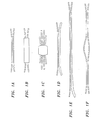
loss 2 × 2 coupler is a directional coupler (shown in FIG. 1(a), also called an evanescent coupler), which includes two waveguides arranged in close proximity to allow coupling of light between the waveguides. The splitting ratio of the conventional directional coupler, however, is highly sensitive to: 1) the wavelength of the light propagated through the coupler, 2) the polarization of such light, and 3) variations in the PLC coupler structure (e.g. waveguide width) which can occur during fabrication (hereinafter collectively referred to as wavelength, polarization, and fabrication (WPF) splitting sensitivity). - There are three main approaches to decrease the WPF splitting sensitivity of 2 × 2 couplers: 1) couple to extra modes (i.e., couple the two input modes to many modes inside the coupler and then couple back to two output modes), 2) make the coupler asymmetric, or 3) use multiple sections.
- A multi-mode interference (MMI) coupler (shown in FIG. 1 (b)) is one example of a device for coupling to extra modes. This coupler excites more than two modes in the coupling region. The increased number of modes can decrease the splitting sensitivity to WPF changes because uncertainties are averaged out among many modes. However, MMI couplers typically exhibit undesirable excess loss, and are sensitive to waveguide-width variations that occur during PLC fabrication. Another example of a multimode coupler is the star coupler (shown in FIG. 1(c)). However, as with the MMI coupler, 2 x 2 star couplers typically exhibit high excess loss.
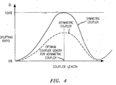
- An asymmetric coupler (shown in FIG. 1 (d)) is a directional coupler having two coupled waveguides of different widths. In directional couplers, the splitting ratio varies sinusoidally between 0% and some value (R) as the coupler length is varied (see FIG. 4). In a symmetric coupler, R is 100%. In an asymmetric coupler, R is < 100% (since the asymmetric nature causes already coupled light to become out of phase with newly in-coupled light before 100% of the light can be coupled over as the coupler length is increased). Asymmetric couplers are typically designed such that R is a desired splitting ratio, and the coupler length is selected such that the splitting ratio achieved is near the peak of the sinusoid (see FIG. 4). Thus, the first-order dependence of the coupling ratio on the length is removed. Asymmetric couplers, however, are highly sensitive to variations of the waveguide width from a desired width, which can occur during PLC fabrication.
- Another example of an asymmetric coupler is the "adiabatic coupler" (shown in FIG. 1 (e)). The waveguides of the adiabatic coupler are asymmetric at one end of the coupling region and symmetric at the other end. The operation principle for these couplers is that the couplers vary from symmetric to asymmetric so gradually that each of the two eigenmodes of the local waveguide structure at the symmetric end convert perfectly to each of the two eigenmodes of the local waveguide structure at the asymmetric end. Adiabatic couplers, however, are comparatively very long thus increasing device size and cost.
- Finally, multi-section couplers (e.g. the two section coupler shown in FIG. 1 (f)) include two or more directional couplers connected with waveguides having a small path-length difference. The small path-length differences are chosen such that the WPF-dependences (or sensitivities) of the directional couplers partially cancel each other out. Two-coupler, three-coupler, and four-coupler multi-section couplers have been proposed and demonstrated. These multi-section couplers, however, are very long thus increasing device size and cost.
- The present invention provides a PLC coupler apparatus for coupling of optical signals with improved wavelength, polarization, and fabrication sensitivity. PLC couplers in accordance with the present invention with waveguides arranged in a curved configuration cause the coupler to have a maximum possible splitting ratio, as wavelength, polarization, or fabrication are varied, that is less than 100%. By making this maximum possible splitting ratio equal to a desired splitting ratio and setting the coupler length such that the actual splitting ratio is equal to the desired splitting ratio when the parameter of interest (e.g., the center wavelength of the coupler) is equal to the desired one, the first-order dependence of the splitting ratio on the parameter of interest is removed.
- Additionally, both waveguides of the coupler can be narrow, which allows the width of the waveguides to be a minimum mode width, making the coupler much less sensitive to waveguide width variations compared to conventional asymmetric couplers. Furthermore, making both waveguides narrow increases the coupling strength, allowing the coupler to be shorter than conventional asymmetric coupler thus reducing PLC fabrication cost.
- In one preferred embodiment, a substantially wavelength and polarization insensitive PLC coupler is provided. The PLC coupler comprises a first waveguide including a curved coupling portion with a radius of curvature Rc1, and a second waveguide including a curved coupling portion with a radius of curvature Rc2. The coupling portion of the second waveguide is operatively coupled to the coupling portion of the first waveguide such that light can be coupled between the first and second waveguides.
- The foregoing summary, as well as the following detailed description of preferred embodiments of the invention, will be better understood when read in conjunction with the appended drawings. For the purpose of illustrating the invention, there are shown in the drawings embodiments that are presently preferred. It should be understood, however, that the invention is not limited to the precise arrangements and instrumentalities shown.
In the drawings: - FIGS. 1(a)-(f) are illustrations of prior art couplers;
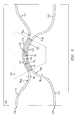
- FIG. 2 is an illustration of a PLC coupler according to one embodiment of the invention;
- FIGS. 3(a)-(b) are plots showing the measured transmissivity vs. wavelength for a straight coupler, and a PLC coupler according to an embodiment of the invention;
- FIG. 3(c) is a plot showing the splitting ratio vs. wavelength for a straight coupler and a PLC coupler according to an embodiment of the invention; and
- FIG. 4 is a plot graphically illustrating the splitting ratio vs. coupler length for symmetric and asymmetric couplers.
- FIG. 2 is an illustration of one embodiment of a
PLC coupler 100 according to the invention. ThePLC coupler 100 preferably comprises afirst waveguide 110 and asecond waveguide 120. Each of the first andsecond waveguides input portion curved coupling portion coupling region 130, and anoutput portion - The input and
output portions output waveguides - The
curved coupling portions second waveguides coupling region 130 such that light in the first orsecond waveguides waveguides curved coupling portions PLC coupler 100 is equal to a desired splitting ratio. Thecoupling portions second waveguides PLC coupler 100 exhibits a maximum splitting ratio in a desired wavelength range. - When Rc1 and Rc2 are finite, light coupled from, for example, the
first waveguide 110 to thesecond waveguide 120 travels a different distance than light traveling only in the first waveguide 110 (i.e. uncoupled light). This results in light that couples into thesecond waveguide 120 later in the coupling region being out of phase with previously coupled light before 100% of the light couples over. Coupling of light out of phase causes destructive interference thus preventing additional coupling. Therefore, the maximum possible splitting ratio when Rc1 and Rc2 are finite is less than 100% regardless of coupler length or wavelength. - A
gap 135 having a desired width is formed between thecoupling portions second waveguides 110, 120 (with Rc being the radius of curvature of a centerline extending in thegap 135 in the coupling region). Preferably, the width of thegap 135 is selected to be the smallest gap that can be formed on the PLC without creating significant fabrication difficulty (e.g. asymmetry in the etching of the first and thesecond waveguides 110, 120). It will be understood by those skilled in the art that asmaller gap 135 produces stronger coupling, which allows for a shorter coupler with less wavelength dependence. - The propagation constants of the first and
second waveguides PLC coupler 100 is substantially wavelength and polarization insensitive. The splitting ratio of thePLC coupler 100 preferably varies by less than ~10% over a frequency range of~200nm around a desired center wavelength. - The width (w1) of the
first waveguide 110 and the width (w2) of thesecond waveguide 120 are preferably selected to be about the minimum mode width (i.e. the point at which the fundamental mode in the waveguide has a minimum width). Such a minimum mode width provides improved insensitivity to waveguide width changes. Formulae for calculating R c (and accordingly Rc1 and Rc2) and Lc can be derived, provided Ls, the length of the coupling region of a straight coupler, is known (Rc and Lc are respectively the radius of curvature and length of a centerline of the gap between the coupler waveguides in thecoupling region 130, as shown in FIG. 2). Starting with the coupling of modes equations:
where a i is the field and β i is the effective propagation constant in guide i, κ 12 and κ 21 are the coupling coefficients, and j is the square root of -1. By effective propagation constant we mean the propagation constant using the distance z along the centerline of the gap between the waveguides as the frame of reference. These equations are valid provided |κ|<<|β|, which is the case for typical directional couplers. - If we start with zero field in a first waveguide (guide 1) and field with amplitude α2(0) in a second waveguide (guide 2), the solution for a 1 is


where C is the desired splitting ratio, s is the center-to-center spacing between waveguides in the coupling region, n is the refractive index, and λ is the vacuum wavelength. For example, for a 50/50 coupler C = 0.5. Thus, if one has a reasonably good estimate of the length of a straight 100/0 coupler Eq. (3) can be used to approximately determine the structure of a curved PLC coupler according to embodiments of the invention to provide a WPF desensitized coupler with splitting ratio C. It will be appreciated by those skilled in the art that small modifications to Lc and Rc (obtained through straightforward simulations or experimentation), may be used to more precisely achieve the desired splitting ratio C at the desired wavelength λ. - It is noted that the contributions from the coupler input and output portions (e.g. 111, 121, 113, 123) were not included in the above calculations. Those skilled in the art will appreciate that although these contributions can be quite significant (e.g. together contributing ~37% of the total coupling in a typical straight 50/50 coupler), because the contributions were ignored for both straight and curved couplers according to the invention when deriving Eq. (3), Eq. (3) is sufficiently accurate to use as an initial design guideline. For example, if a design for a straight 50/50 directional coupler is established, with L s =500 µm, the design of a 50/50 curved coupler can be detennined. First, the straight length for a 100/0 straight coupler is estimated, which would be -(2-0.37)/(1-0.37) x 500 µm = 1300 µm. Then using Eq. (3), L c = 919 µm. Rc can also be calculated from (3), using the s of the straight coupler.
- Experimental 50/50 couplers in silica-on-silicon waveguides with a 0.80%-index contrast and 6.0-µm core height were constructed to test aspects of the invention. A conventional straight directional coupler was made, with waveguide width = 4.3 µm, gap = 3.95 µm, R io = 10 mm, and L s = 620 µm. A curved PLC coupler according to embodiments of the invention was made next to the conventional straight coupler with waveguide width = 4.3 µm, gap = 3.9 µm, R io = 10 mm, R c = 27 mm, and L c = 1178 µm. If portions of the input and output waveguide portions are included in calculating the total coupler length to where the waveguides are fully uncoupled (e.g., ~19 µm apart, giving a total length on each side for the input/output waveguides of 320 µm long), then the total length of the curved PLC coupler is only 1.4 times the total length of the straight coupler.
- FIGS. 3(a)-(b) respectively show plots of the measured transmissivities for both transverse electric (TE) and transverse magnetic (TM) polarizations of the straight coupler and the curved PLC coupler according to the invention vs. wavelength over the C and L bands. The measured losses are the fiber-to-fiber losses. Those skilled in the art will appreciate that the curved PLC coupler is much less sensitive than the straight coupler to both wavelength and polarization yet has no additional loss. FIG. 3(c) shows plots of the measured splitting ratios of the straight coupler and the curved PLC coupler according to the invention vs. wavelength over the C and L bands. Across the C and L bands the splitting ratio of the straight coupler varies by ~20%, whereas the splitting ratio of the curved PLC coupler varies by less than ~5%.
- Simulations were also conducted to determine the fabrication sensitivity of curved PLC couplers according to embodiments of the invention. Using 2-D beam propagation, a curved PLC coupler was compared to a straight asymmetric coupler (using similar parameters given above), with one waveguide 4.3 µm wide and the other 5.1 µm wide. Ls = 1000 µm. Both couplers were designed and verified to be wavelength-insensitive at □ λ = 1550 nm. Decreasing all the waveguide widths by 0.3 µm on each side changed the curved PLC coupler coupling ratio from 50/50 to 48/52, whereas the straight asymmetric coupler coupling ratio changed from 50/50 to 28/72. In another simulation, we confirmed that the wavelength-sensitivity of the curved PLC coupler becomes even flatter when the center-to-center spacing between the waveguides in the
coupling region 130 is decreased. - It is understood that one potential drawback to a desensitized coupler is that a reduced WPF sensitivity in splitting ratio may result in an increased WPF sensitivity in phase difference between the output signals when the coupler is excited at a single input. Calculations were conducted to study the relationship between splitting sensitivity and phase difference sensitivity.
- The operation of single-section couplers can be described by the matrix R -1(θ1)P(φ)R(θ2), where R and P are:

- The table below shows four different choices for θ1, φ, and θ2 that give a 50/50 splitting ratio and the resultant errors in splitting ratio and phase difference between the ports.
Name θ1 φ θ2 Power splitting error Phase error from left side Phase error from right side Conventional straight coupler 


0 0 Constant curvature 
π 
1.2ε 2 

Small variation in curvature 
π 
0.7ε2 0.31πε 0.95πε Large variation in curvature (adiabatic coupler) 
>> π 0 0 0 >> πε - Those skilled in the art will appreciate from the table that the lower the power splitting error the higher the worst-case phase error. For instance, the conventional straight coupler has the worst splitting sensitivity but zero error in phase, whereas the curved coupler with a large variation in curvature (i.e., an adiabatic coupler) has theoretically zero power splitting error but very large phase error at one end of the coupler.
- The increased phase sensitivity may cause problems in some devices. For example, an MZI switch using curved PLC couplers in accordance with embodiments of the present invention may have a switch state driving phase that is highly WPF sensitive. One solution to this problem is to use two curved PLC couplers according to embodiments of the invention, oppositely oriented, in an MZI. Provided the environment and design is the same for both curved PLC couplers, any phase change in one coupler will be canceled by that of the other coupler.
- It will be understood by those skilled in the art that Rc1 and Rc2 may be varied over the lengths (Lc1, Lc2) of the coupling portions of the first and
second waveguides coupling region 130 to the other. - It will be appreciated by those skilled in the art that changes could be made to the embodiments described above without departing from the broad inventive concept thereof. It is understood, therefore, that this invention is not limited to the particular embodiments disclosed, but it is intended to cover modifications within the spirit and scope of the present invention as defined by the appended claims.
Claims (9)
- A planar lightwave circuit (PLC) coupler comprising:a first waveguide including a curved coupling portion with a finite radius of curvature Rc1; anda second waveguide including a curved coupling portion with a finite radius of curvature Rc2, the coupling portion of the second waveguide being operatively coupled to the coupling portion of the first waveguide such that light can be coupled between the first and second waveguides;wherein the propagation constants of the first and second waveguides are substantially the same; and
wherein the splitting ratio of the coupler is substantially wavelength and polarization insensitive. - The coupler of claim 1, wherein the splitting ratio of the coupler varies by less than about 10% over a frequency range of about 100nm around a desired center wavelength.
- The coupler of claim 1, wherein the width of the first waveguide (w1) and the width of the second waveguide (w2) are selected such that the fundamental mode in each waveguide has a minimum width.
- The coupler of claim 1, wherein Rc1 and Rc2 are constant over their respective curved coupling portions.
- The coupler of claim 1, wherein the input and output portions of the first and second waveguides have substantially the smallest radii of curvature without causing significant bend radiation loss.
- The coupler of claim 1, wherein Rc1 and Rc2 are selected such that the maximum possible splitting ratio for the PLC coupler is equal to a desired splitting ratio.
- The coupler of claim 6 wherein the lengths (Lc1, Lc2) of the coupling portions of the first and second waveguides are selected such that the coupler exhibits maximum splitting ratio in a desired wavelength range.
- The coupler of claim 1, wherein Rc1 and Rc2 vary over the lengths (Lc1, Lc2) of the coupling portions of the first and second waveguides such that a desired power splitting sensitivity and a desired phase sensitivity for the coupler are achieved.
- A method of fabricating a planar lightwave circuit (PLC) for optical coupling comprising the steps of:forming a first waveguide and a second waveguide on a PLC, the first waveguide and the second waveguide having curved coupling regions with finite radii of curvature Rc1 and Rc2, respectively;wherein the propagation constants of the first and second waveguides are substantially the same, and Rc1 and Rc2 are selected such that the coupler exhibits a desired splitting ratio, and
wherein the splitting ratio of the coupler is substantially wavelength and polarization insensitive.
Applications Claiming Priority (1)
| Application Number | Priority Date | Filing Date | Title |
|---|---|---|---|
| US11/089,640 US7302137B2 (en) | 2005-03-25 | 2005-03-25 | Optical coupler apparatus and method |
Publications (2)
| Publication Number | Publication Date |
|---|---|
| EP1712937A2 true EP1712937A2 (en) | 2006-10-18 |
| EP1712937A3 EP1712937A3 (en) | 2006-12-06 |
Family
ID=36660681
Family Applications (1)
| Application Number | Title | Priority Date | Filing Date |
|---|---|---|---|
| EP06251058A Withdrawn EP1712937A3 (en) | 2005-03-25 | 2006-02-28 | Optical curved directional coupler and method |
Country Status (4)
| Country | Link |
|---|---|
| US (1) | US7302137B2 (en) |
| EP (1) | EP1712937A3 (en) |
| JP (1) | JP2006276857A (en) |
| CN (1) | CN1837873A (en) |
Cited By (1)
| Publication number | Priority date | Publication date | Assignee | Title |
|---|---|---|---|---|
| CN111708116A (en) * | 2020-07-17 | 2020-09-25 | 南京大学 | A high-density integrated optical waveguide |
Families Citing this family (18)
| Publication number | Priority date | Publication date | Assignee | Title |
|---|---|---|---|---|
| EP1987382B1 (en) * | 2006-02-24 | 2022-04-20 | NeoPhotonics Corporation | Broadband 2x2 optical splitter |
| US7742666B2 (en) * | 2008-08-25 | 2010-06-22 | Fujitsu Limited | Optical beam splitter |
| US9170438B2 (en) * | 2012-07-10 | 2015-10-27 | Infinera Corporation | Suppression of resonant polarization conversion in photonic integrated circuits |
| JP2014041175A (en) * | 2012-08-21 | 2014-03-06 | Oki Electric Ind Co Ltd | Wavelength selective optical route switching device |
| US20140217269A1 (en) * | 2013-02-01 | 2014-08-07 | The Board Of Trustees Of The Leland Stanford Junior University | Coupled waveguides for slow light sensor applications |
| JP6424018B2 (en) * | 2014-06-06 | 2018-11-14 | 株式会社フジクラ | Mode conversion element and optical waveguide element |
| JP6346796B2 (en) * | 2014-06-06 | 2018-06-20 | 株式会社フジクラ | Mode conversion element and optical waveguide element |
| CN105743519B (en) * | 2016-04-07 | 2019-01-29 | 锐迪科微电子(上海)有限公司 | A kind of radio frequency transmitter circuitry, bidirectional coupler and directional coupler |
| CN106054317B (en) * | 2016-06-03 | 2019-11-15 | 浙江大学 | A polarization-insensitive microring filter based on a silicon nanowire waveguide |
| CN106405733B (en) * | 2016-10-26 | 2019-02-15 | 浙江大学 | A polarization beam splitter-beam combiner |
| CN110187439B (en) * | 2019-05-07 | 2020-11-13 | 南京邮电大学 | A polarization independent beam splitter |
| US11921320B2 (en) * | 2019-06-04 | 2024-03-05 | Nippon Telegraph And Telephone Corporation | Optical circuit |
| CN113009621B (en) * | 2019-12-19 | 2024-09-24 | 中兴光电子技术有限公司 | Directional coupler and beam splitter thereof |
| KR102490915B1 (en) * | 2020-07-14 | 2023-01-20 | 서울시립대학교 산학협력단 | Mach-zehnder interferometer and sensor using the same |
| CN114077773A (en) * | 2020-08-19 | 2022-02-22 | 中兴光电子技术有限公司 | Adiabatic coupling waveguide section design method of adiabatic coupler, and apparatus and equipment thereof |
| CN112162352A (en) * | 2020-09-09 | 2021-01-01 | 山东建筑大学 | A Continuously Adjustable Spectral Ratio Directional Coupler Based on Parity-Time Symmetry |
| CN116520492A (en) * | 2023-04-23 | 2023-08-01 | 中国科学院上海微系统与信息技术研究所 | Directional coupling device |
| CN119355871B (en) * | 2024-10-11 | 2025-07-22 | 广州铌奥光电子有限公司 | Curved waveguide directional coupler with adjustable splitting ratio |
Family Cites Families (9)
| Publication number | Priority date | Publication date | Assignee | Title |
|---|---|---|---|---|
| US4737007A (en) * | 1986-02-24 | 1988-04-12 | American Telephone And Telegraph Company, At&T Bell Laboratories | Narrow-band wavelength selective optical coupler |
| JPS6371377A (en) | 1986-09-12 | 1988-03-31 | Canon Inc | Electronic machinery with printer |
| JPH0778585B2 (en) * | 1988-03-24 | 1995-08-23 | 日本電気株式会社 | Directional coupler type optical waveguide switch |
| JP2927795B2 (en) * | 1988-03-29 | 1999-07-28 | 日本電気株式会社 | Light switch |
| GB2223323B (en) * | 1988-06-04 | 1992-08-12 | Plessey Co Plc | Optical devices using curved, concentric coupled optical waveguides |
| GB9018384D0 (en) * | 1990-08-22 | 1990-10-03 | Marconi Gec Ltd | Integrated optic waveguide coupler |
| JPH08184720A (en) * | 1994-12-28 | 1996-07-16 | Hitachi Cable Ltd | Waveguide element |
| US5495544A (en) * | 1995-03-22 | 1996-02-27 | Minnesota Mining And Manufacturing Company | Polarization-independent electro-optically switched directional coupler |
| JP2001318253A (en) * | 2000-05-12 | 2001-11-16 | Furukawa Electric Co Ltd:The | Optical waveguide directional coupler and optical waveguide circuit using the optical waveguide directional coupler |
-
2005
- 2005-03-25 US US11/089,640 patent/US7302137B2/en active Active
-
2006
- 2006-02-28 EP EP06251058A patent/EP1712937A3/en not_active Withdrawn
- 2006-03-24 CN CNA2006100680551A patent/CN1837873A/en active Pending
- 2006-03-24 JP JP2006082205A patent/JP2006276857A/en not_active Abandoned
Cited By (2)
| Publication number | Priority date | Publication date | Assignee | Title |
|---|---|---|---|---|
| CN111708116A (en) * | 2020-07-17 | 2020-09-25 | 南京大学 | A high-density integrated optical waveguide |
| CN111708116B (en) * | 2020-07-17 | 2021-06-08 | 南京大学 | High-density integrated optical waveguide |
Also Published As
| Publication number | Publication date |
|---|---|
| CN1837873A (en) | 2006-09-27 |
| JP2006276857A (en) | 2006-10-12 |
| EP1712937A3 (en) | 2006-12-06 |
| US20060215957A1 (en) | 2006-09-28 |
| US7302137B2 (en) | 2007-11-27 |
Similar Documents
| Publication | Publication Date | Title |
|---|---|---|
| EP1712937A2 (en) | Optical curved directional coupler and method | |
| JP6475626B2 (en) | Curved optical waveguide | |
| US7317853B2 (en) | Integrated optics spot size converter and manufacturing method | |
| EP1936322B1 (en) | Interferometer and its fabrication method | |
| EP2180361B1 (en) | Polarization-independent waveguide-type optical interference circuit | |
| EP1118888B1 (en) | Polarization independent waveguide type optical circuit | |
| JPH06194539A (en) | Optical interconnection device | |
| Doerr et al. | Bending of a planar lightwave circuit 2/spl times/2 coupler to desensitize it to wavelength, polarization, and fabrication changes | |
| JP7328580B2 (en) | optical waveguide | |
| Yamada et al. | Microphotonics devices based on silicon wire waveguiding system | |
| US7062130B2 (en) | Low-loss optical waveguide crossovers using an out-of-plane waveguide | |
| US20010036338A1 (en) | Optical transmission module and optical communication system using the same | |
| US6950581B2 (en) | Optical coupler apparatus and methods having reduced geometry sensitivity | |
| CN103238093A (en) | Optical branching element, optical waveguide device by using optical branching element, and method of manufacturing optical branching element, method of manufacturing optical waveguide device | |
| EP1058137B1 (en) | Method of manufacturing polarization-maintaining optical fiber coupler | |
| EP1239311A1 (en) | Integrated optical device comprising an adiabatic junction | |
| US7555180B2 (en) | Optical branching component with low polarisation sensitivity and increased process tolerance | |
| WO2019117313A1 (en) | Optical polarization wave element and method for manufacturing same | |
| Le | Design of a polarization independent MMI SOI coupler based microresonator using sandwich structures | |
| EP1393104B1 (en) | Waveguide bends and devices including waveguide bends | |
| JP7280534B2 (en) | optical waveguide | |
| EP4312067A1 (en) | Broadband ring resonator and design system thereof | |
| JP5333031B2 (en) | Optical branching element and manufacturing method thereof | |
| Yun | Silicon Photonic Components using Sub-wavelength Gratings and other Periodic Structures | |
| Samanta et al. | Design and Analysis of Directional Coupler made of Straight and Curved Silicon wire waveguides |
Legal Events
| Date | Code | Title | Description |
|---|---|---|---|
| PUAI | Public reference made under article 153(3) epc to a published international application that has entered the european phase |
Free format text: ORIGINAL CODE: 0009012 |
|
| 17P | Request for examination filed |
Effective date: 20060315 |
|
| AK | Designated contracting states |
Kind code of ref document: A2 Designated state(s): AT BE BG CH CY CZ DE DK EE ES FI FR GB GR HU IE IS IT LI LT LU LV MC NL PL PT RO SE SI SK TR |
|
| AX | Request for extension of the european patent |
Extension state: AL BA HR MK YU |
|
| PUAL | Search report despatched |
Free format text: ORIGINAL CODE: 0009013 |
|
| AK | Designated contracting states |
Kind code of ref document: A3 Designated state(s): AT BE BG CH CY CZ DE DK EE ES FI FR GB GR HU IE IS IT LI LT LU LV MC NL PL PT RO SE SI SK TR |
|
| AX | Request for extension of the european patent |
Extension state: AL BA HR MK YU |
|
| 17Q | First examination report despatched |
Effective date: 20070130 |
|
| AKX | Designation fees paid |
Designated state(s): DE FR GB |
|
| RAP3 | Party data changed (applicant data changed or rights of an application transferred) |
Owner name: LUCENT TECHNOLOGIES INC. |
|
| STAA | Information on the status of an ep patent application or granted ep patent |
Free format text: STATUS: THE APPLICATION IS DEEMED TO BE WITHDRAWN |
|
| 18D | Application deemed to be withdrawn |
Effective date: 20110901 |