CN1837873A - Optical coupler apparatus and method - Google Patents
Optical coupler apparatus and method Download PDFInfo
- Publication number
- CN1837873A CN1837873A CNA2006100680551A CN200610068055A CN1837873A CN 1837873 A CN1837873 A CN 1837873A CN A2006100680551 A CNA2006100680551 A CN A2006100680551A CN 200610068055 A CN200610068055 A CN 200610068055A CN 1837873 A CN1837873 A CN 1837873A
- Authority
- CN
- China
- Prior art keywords
- coupling mechanism
- waveguide
- coupling
- splitting ratio
- plc
- Prior art date
- Legal status (The legal status is an assumption and is not a legal conclusion. Google has not performed a legal analysis and makes no representation as to the accuracy of the status listed.)
- Pending
Links
Images


Classifications
-
- G—PHYSICS
- G02—OPTICS
- G02B—OPTICAL ELEMENTS, SYSTEMS OR APPARATUS
- G02B6/00—Light guides; Structural details of arrangements comprising light guides and other optical elements, e.g. couplings
- G02B6/10—Light guides; Structural details of arrangements comprising light guides and other optical elements, e.g. couplings of the optical waveguide type
- G02B6/12—Light guides; Structural details of arrangements comprising light guides and other optical elements, e.g. couplings of the optical waveguide type of the integrated circuit kind
- G02B6/12007—Light guides; Structural details of arrangements comprising light guides and other optical elements, e.g. couplings of the optical waveguide type of the integrated circuit kind forming wavelength selective elements, e.g. multiplexer, demultiplexer
-
- G—PHYSICS
- G02—OPTICS
- G02B—OPTICAL ELEMENTS, SYSTEMS OR APPARATUS
- G02B6/00—Light guides; Structural details of arrangements comprising light guides and other optical elements, e.g. couplings
- G02B6/10—Light guides; Structural details of arrangements comprising light guides and other optical elements, e.g. couplings of the optical waveguide type
- G02B6/12—Light guides; Structural details of arrangements comprising light guides and other optical elements, e.g. couplings of the optical waveguide type of the integrated circuit kind
- G02B6/122—Basic optical elements, e.g. light-guiding paths
- G02B6/125—Bends, branchings or intersections
-
- G—PHYSICS
- G02—OPTICS
- G02B—OPTICAL ELEMENTS, SYSTEMS OR APPARATUS
- G02B6/00—Light guides; Structural details of arrangements comprising light guides and other optical elements, e.g. couplings
- G02B6/10—Light guides; Structural details of arrangements comprising light guides and other optical elements, e.g. couplings of the optical waveguide type
- G02B6/12—Light guides; Structural details of arrangements comprising light guides and other optical elements, e.g. couplings of the optical waveguide type of the integrated circuit kind
- G02B2006/12133—Functions
- G02B2006/12147—Coupler
Abstract
A planar lightwave circuit coupler including first and second waveguides with curved coupling portions having radii of curvature selected such that the coupler has a splitting ratio that is substantially wavelength and polarization insensitive.
Description
Technical field
The present invention relates generally to be used for the method and apparatus of coupling optical signal, and relate more particularly to have planar lightwave circuit (PLC) coupling mechanism of improved wavelength and polarization sensitive.
Background technology
Photo-coupler is used for various planar lightwave circuits (PLC), and these circuit for example comprise switch based on Mach-Zehnder interferometer (MZI), first-class based on wave filter, the tap of MZI.2 * 2 coupling mechanisms of loss minimum are directed (directional) coupling mechanisms (shown in Fig. 1 (a), being also referred to as mistake (evanescent) coupling mechanism that fades), and they two waveguides that comprise tight setting are to allow the optically-coupled between the waveguide.But the splitting ratio of traditional directional coupler is to 1) light wavelength, 2 propagated by coupling mechanism) such polarisation of light and 3) variation (hereinafter be collectively referred to as wavelength, polarization and manufacturing (WPF) and distribute (split) susceptibility) of the PLC coupler structure (for example waveguide length) that takes place during manufacture is very responsive.
Exist three kinds of main WPF that reduce 2 * 2 coupling mechanisms to distribute the method for susceptibility: 1) be coupled to outside mould (even two input mode couplings many moulds in the coupling mechanism, and be coupled back then two export moulds), 2) make coupling mechanism asymmetric or 3) use a plurality of parts.
Multiple-mode interfence (MMI) coupling mechanism (shown in Fig. 1 (b)) is an example that is used to be coupled to the equipment of outside mould.This coupling mechanism is at unnecessary two mould of coupling regime underexcitation.The increase of the quantity of mould can reduce the distribution susceptibility to the WPF variation, and this is average because of uncertainty between a plurality of moulds.But the MMI coupling mechanism shows undesirable excess loss usually, and changes responsive to the duct width that takes place during making at PLC.Another example of multi-mode coupler is star-type coupler (shown in Fig. 1 (c)).But similar with the MMI coupling mechanism, 2 * 2 star-type couplers show the outer loss of great number usually.
Asymmetric coupling mechanism (Fig. 1 (d) in shown in) is the directional coupler of waveguide with different in width of two couplings.In directional coupler, along with coupler length changes, splitting ratio 0% and some values (R) between the sinusoidal variations (see figure 4).R is 100% in symmetric couplers.R is less than 100% (because when coupler length increases, before the light 100% can be coupled into, asymmetric essence made light that has been coupled and the light out-phase that is coupled into recently) in asymmetric coupling mechanism.Asymmetric coupling mechanism is designed such that usually R is the splitting ratio of expection, and coupler length is selected as making the splitting ratio that realizes near sinusoidal wave summit (see figure 4).Therefore, eliminated the single order dependence of coupling ratio to length.But asymmetric coupling mechanism is very responsive to the variation that the duct width that can take place during PLC makes departs from expected width.
Another example of asymmetric coupling mechanism is " adiabatic (adiabatic) coupling mechanism " (as shown in Fig. 1 (e)).The waveguide of adiabatic coupler is asymmetric and be symmetrical at the other end at an end of coupling regime.It is asymmetric that the principle of work of these coupling mechanisms is that coupling mechanism changes to from symmetry gradually, thereby in two natural mode of vibration (eigenmode) of the local waveguiding structure at symmetry end place each is converted in two natural mode of vibration of the local waveguiding structure at asymmetric end place each well.But adiabatic coupler is quite long, thereby equipment size and cost increase.
At last, multi-section coupler (two parts coupling mechanism shown in for example, in Fig. 1 (f)) comprises the two or more directional couplers that are connected by the waveguide with small path length difference.The small path length difference is selected as making the WPF dependence (or susceptibility) of directional coupler partly to cancel out each other.Two coupling mechanisms, three coupling mechanisms and four coupling mechanism multi-section couplers have been proposed and have illustrated.But these multi-section couplers are very long, thereby equipment size and cost increase.
Summary of the invention
The invention provides a kind of PLC coupler device that is used for coupling optical signal with improved wavelength, polarization and manufacturing susceptibility.The PLC coupling mechanism according to the present invention that has with the waveguide of curved configuration setting can make coupling mechanism have the maximum possible splitting ratio, and when changing wavelength, polarization or making, this splitting ratio is less than 100%.Make when the parameter that the parameter of being concerned about (for example centre wavelength of coupling mechanism) equals to expect actual splitting ratio equal to expect splitting ratio by making the splitting ratio that this maximum possible splitting ratio equals to expect and coupler length being set, can eliminate the single order dependence of splitting ratio this parameter of being concerned about.
In addition, two waveguides of coupling mechanism may be narrow, and this allows the width of waveguide is the minimum modulus width, makes this coupling mechanism and traditional asymmetric coupling mechanism compare duct width and change more insensitive.In addition, make two Narrow Wall of Waveguide can increase stiffness of coupling, allow coupling mechanism shorter, thereby reduce the PLC manufacturing cost than traditional asymmetric coupling mechanism.
In a preferred embodiment, provide substantially to wavelength and the insensitive PLC coupling mechanism of polarization.This PLC coupling mechanism comprises first waveguide and second waveguide, and this first waveguide comprises that radius-of-curvature is R
C1Crooked coupling unit, this second waveguide comprises that radius-of-curvature is R
C2Crooked coupling unit.The coupling unit of this second waveguide operationally is coupled to the coupling unit of this first waveguide, thereby light can be coupled between this first and second waveguide.
Description of drawings
When reading in conjunction with the accompanying drawings, can understand preamble general introduction and the following detailed description of the embodiment of the present invention better.For the present invention being described, currently preferred embodiment shown in the drawings.However, it should be understood that accurate setting and the instrument of the present invention shown in being not limited to.
In the accompanying drawings:
Fig. 1 (a)-(f) illustrates the coupling mechanism of prior art;
Fig. 2 illustrates PLC coupling mechanism according to an embodiment of the invention;
Fig. 3 (a)-(b) be illustrate straight coupling mechanism and according to an embodiment of the invention the measured transmittance of PLC coupling mechanism in contrast to the curve of wavelength;
Fig. 3 (c) be illustrate straight coupling mechanism and according to an embodiment of the invention the splitting ratio of PLC coupling mechanism in contrast to the curve of wavelength;
Fig. 4 illustrates the curve that symmetry and the splitting ratio of asymmetric coupling mechanism in contrast to coupler length.
Embodiment
Fig. 2 is the diagram according to an embodiment of PLC coupling mechanism 100 of the present invention.PLC coupling mechanism 100 preferably includes first waveguide 110 and second waveguide 120.In this first and second waveguide 110,120 each comprises importation 111,121 respectively, crooked coupling unit 112,122 in coupling regime 130 and output 113,123.
The input and output part 111,121,113,123 of first and second waveguides preferably has radius of curvature R
Io1, R
Io2, R
Io3, R
Io4(or " bending radius "), this radius-of-curvature are minimum and can not produce very big crooked radiation loss so that to the contribution minimum from the coupling of I/O waveguide 111,121,113,123 under possible condition substantially.
The crooked coupling unit 112,122 of first and second waveguides 110,120 is operatively coupling (for example closely placing) in coupling regime 130, thereby the light in first or second waveguide 110,120 is coupled between waveguide 110,120.Crooked coupling unit 112,122 has radius of curvature R respectively
C1And R
C2R
C1And R
C2Preferably be selected as making the splitting ratio that the maximum possible splitting ratio of PLC coupling mechanism 100 equals to expect.The length of the coupling unit 112,122 of first and second waveguides 110,120 is L
C1, L
C2L
C1And L
C2Be selected as preferably making that PLC coupling mechanism 100 shows maximum splitting ratio in the wavelength coverage of expection.
Work as R
C1And R
C2When being limited, it is different to be coupled to the distance that the light distance of advancing and the light of only advancing (promptly not coupling light) of second waveguide 120 advances from for example first waveguide 110 in first waveguide 110.This caused before 100% optically-coupled, be coupled to after a while light in second photoconduction 120 in coupling regime with the light out-phase that was coupled in the past.The out-phase coupling of light can cause destructive interference, thereby prevents extra coupling.Therefore, no matter coupler length or wavelength are how, at R
C1And R
C2Maximum possible splitting ratio when being limited is always less than 100%.
Between the coupling unit 112,122 of first and second waveguides 110,120, form gap 135 (R with expected width
cBe the radius-of-curvature of the center line of extension in the gap 135 in coupling unit).Preferably, the width in gap 135 be selected as on PLC, forming and can not produce the minimum clearance of serious manufacturing difficulty (for example, etching first and second waveguides asymmetric) at 110,120 o'clock.Those skilled in the art should be understood that less gap 135 can produce than strong coupling, and this allows to have the shorter coupling mechanism of less wavelength dependency.
The propagation constant of first and second waveguides 110,120 is preferably basic identical.The splitting ratio of PLC coupling mechanism 100 is insensitive to wavelength and polarization substantially.The splitting ratio of PLC coupling mechanism 100 preferably around the expection centre frequency~change less than~10% in the frequency range of 200nm.
Width (the w of first waveguide 110
1) and the width (w of second waveguide 120
2) preferably be selected as about minimum modulus width (that is, the basic mode in the waveguide has the position of minimum widith).Such minimum modulus width provide improved to duct width change insensitive.Suppose the length L of the coupling regime of known straight coupling mechanism, then can obtain being used to calculate R
c(with the R of correspondence
C1And R
C2) and L
cFormula (R as shown in Figure 2,
cAnd L
cBe respectively the radius-of-curvature and the length of the center line in the gap between the coupled waveguide in coupling regime 130).Begin with the mode coupling formula:
A wherein
iBe field in the waveguide i and β
iBe the effective propagation constant in the waveguide i, к
12And к
21Be coupling coefficient, and j is-1 square root.We refer to effective propagation constant will be along the distance z of the center line in the gap between waveguide as the propagation constant with reference to system.Suppose | к |<<| β |---this is the situation of traditional directional coupler, and these formula are effective.
If we begin like this, in first waveguide (waveguide 1), in second waveguide (waveguide 2), be a promptly for having amplitude for null field
2(0) field, then a
1Separate for:
If L
S, fullBe the L of straight complete (full) coupling mechanism (100/0 coupling mechanism)
s, supposing then that then comparing к with crooked coupling mechanism does not change, then can find from equation (2):
Wherein C is the splitting ratio of expection, and s is the interval of the center to center between the waveguide in coupling regime, and n is a refractive index, and λ is a vacuum wavelength.For example, for 50/50 coupling mechanism, C=0.5.Therefore, if can make rationally good estimation to the length of 100/0 straight coupling mechanism, the structure that can use equation (3) to determine approx crooked according to an embodiment of the invention PLC coupling mechanism is to provide the WPF with splitting ratio C insensitive coupling mechanism.Those skilled in the art should be understood that and can use L
cAnd R
cLittle modification (obtaining) by direct emulation or experiment come af at wavelength lambda in expection to realize the splitting ratio C that expects more accurately.
Should point out, not comprise contribution in the aforementioned calculation from coupling mechanism input and output part (for example 111,121,113,123).Those skilled in the art should understand, although these contributions very huge (for example contribute altogether total coupling in typical straight 50/50 coupling mechanism~37%), but because all ignored these contributions for the crooked coupling mechanism of direct sum according to the present invention when deriving equation (3), so equation (3) can be enough exactly as the initial designs guide.For example, if set up the design of 50/50 straight coupling mechanism, then utilize L
s=500 μ m can determine the design of 50/50 crooked coupling mechanism.At first, estimate the straight length of 100/0 straight coupling mechanism, it is~(2-0.37)/(1-0.37) * 500 μ m=1300 μ m.Use equation (3) then, L
c=919 μ m.Also can use the s of straight coupling mechanism to calculate R from (3)
c
Experiment 50/50 coupling mechanism of constructing SiO 2 waveguide on the silicon with 0.80% index contrast degree and 6.0 μ m core height is to test aspect of the present invention.Realize traditional straight directional coupler, its duct width=4.3 μ m, gap=3.95 μ m, R
Io=10mm and L
s=620 μ m.Be close to this traditional straight directional coupler and realize crooked according to an embodiment of the invention PLC coupling mechanism, the duct width of this coupling mechanism=4.3 μ m, gap=3.9 μ m, R
Io=10mm, R
c=27mm and L
s=1178 μ m.If (for example when calculating total coupler length, comprise input and output waveguide part partly that waveguide not have coupling fully, separate~19 μ m, total length on each side of I/O waveguide is 320 μ m), then the total length of crooked then PLC coupling mechanism only is 1.4 times of total length of straight coupling mechanism.
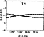
Fig. 3 (a)-3 (b) is illustrated in the straight coupling mechanism on C and the L frequency band respectively and in contrast to the curve of wavelength according to the transmittance of the measurement of the transverse electric (TE) of crooked PLC coupling mechanism of the present invention and transverse magnetic (TM) polarization.Measured loss is loss between optical fiber.One skilled in the art will understand that with straight coupling mechanism and compare that crooked PLC coupling mechanism is much smaller and do not have an excess loss to the susceptibility of wavelength and polarization.Fig. 3 (c) is illustrated in the straight coupling mechanism on C and the L frequency band and in contrast to the curve of wavelength according to the splitting ratio of the measurement of crooked PLC coupling mechanism of the present invention.On C and L frequency band, the splitting ratio of straight coupling mechanism changes~20%, and the splitting ratio of crooked PLC coupling mechanism changes less than~5%.
Also carry out emulation to determine the manufacturing susceptibility of crooked according to an embodiment of the invention PLC coupling mechanism.Use 2 dimension beam propagation, crooked PLC coupling mechanism is compared with straight asymmetric coupling mechanism (using above given identical parameter), a waveguide wide is 4.3 μ m and the wide of another waveguide is 5.1 μ m.L
s=1000μm。It is insensitive that these two coupling mechanisms are designed and are verified as when λ=620 μ m wavelength.On each side all duct widths are reduced 0.3 μ m, the coupling ratio that makes crooked PLC coupling mechanism is changed to 48/52 from 50/50, and the coupling ratio of straight asymmetric coupling mechanism changes to 28/72 from 50/50.In another emulation, the spacing of cut of the center to center of susceptible of proof between the waveguide in the coupling regime 130 after a little while, the wavelength sensitivity of crooked PLC coupling mechanism is more smooth.
A potential defective that should be understood that insensitive coupling mechanism is when with single input stimulus coupling mechanism, and the reducing of the WPF susceptibility of splitting ratio can cause the WPF susceptibility in the phase differential between the output signal to increase.Calculate with the relation between research distribution susceptibility and the phase differential susceptibility.
The operation of single part coupling mechanism can be by matrix R
-1(θ
1) P (φ) R (θ
2) describe, wherein R and P are:
θ is the splitting ratio of two natural modes of coupling mechanism, and φ is the phase shift between two natural modes of coupling mechanism.Supposing that WPF changes causes φ to occur that thereby error φ becomes φ (1+ ε) and θ is error free.ε<<1。This is reasonably for traditional straight coupling mechanism and crooked coupling mechanism according to the present invention, and this is because the WPF variation mainly influences coupling mechanism natural mode propagation constant and can not change the natural mode shape.
Express down and can provide 50/50 splitting ratio and the splitting ratio of generation and the θ of the error in the phase differential between the port
1, φ and θ
2Four different selections.
Those skilled in the art should understand from this table, and the phase error of the low more then worst condition of power division error is high more.For example, it is zero that but the straight coupling mechanism of tradition has the poorest distribution susceptibility phase error, and curvature has the crooked coupling mechanism (being adiabatic coupler) of great changes and has the zero power allocation error in theory, but has very large phase error at an end of coupling mechanism.
The increase of phase sensitivity can cause the problem in some equipment.For example, use the MZI switch of crooked according to an embodiment of the invention PLC coupling mechanism to have and drive the very on off state of the phase place of WPF sensitivity.A solution of this problem is to use towards two opposite crooked according to an embodiment of the invention PLC coupling mechanisms in MZI.The environment of supposing two crooked PLC coupling mechanisms is identical with design, and then the interior any phase change of coupling mechanism all can be offset by the phase change of another coupling mechanism.
Those skilled in the art should be understood that R
C1And R
C2Can be at the length (L of the coupling unit of first and second waveguides 110,120
C1And L
C2) upward change.By changing R
C1And R
C2, can realize the power division susceptibility of expection of this coupling mechanism and the phase sensitivity of expection.For example, for R
C1And R
C2In have the coupling mechanism (go up table the third line) of little variation, R
C1And R
C2Preferably change (for example dull the minimizing or rising) gradually.For R
C1And R
C2The interior big coupling mechanism that changes (going up the fourth line of showing), the R of existing
C1And R
C2Preferably the end to end from coupling unit 130 becomes finite value (or vice versa) from infinitary value.
One skilled in the art will understand that and to change the foregoing description and can not deviate from wide inventive concept of the present invention.Therefore, should understand the present invention and be not limited to disclosed specific embodiment, and will cover the interior modification of the spirit and scope of the present invention that is defined by the following claims.
Claims (9)
1, a kind of planar lightwave circuit (PLC) coupling mechanism, this coupling mechanism comprises:
Comprise and have limited radius of curvature R
C1First waveguide of crooked coupling unit; And
Comprise and have limited radius of curvature R
C2Second waveguide of crooked coupling unit, the coupling unit of this second waveguide operationally is coupled to the coupling unit of this first waveguide, thus light can be coupled between this first and second waveguide;
Wherein the propagation constant of this first and second waveguide is basic identical; And
Wherein the splitting ratio of this coupling mechanism is insensitive to wavelength and polarization substantially.
According to the coupling mechanism of claim 1, it is characterized in that 2, the variation of the splitting ratio of described coupling mechanism in the frequency range of the about 100nm that centers on expection centre wavelength is less than about 10%.
3, according to the coupling mechanism of claim 1, it is characterized in that the width (w of described first waveguide
1) and the width (w of described second waveguide
2) be selected as making that the basic mould in each waveguide has minimum widith.
4, according to the coupling mechanism of claim 1, it is characterized in that, wherein R
C1And R
C2Constant on their crooked coupling units separately.
According to the coupling mechanism of claim 1, it is characterized in that 5, the input and output of wherein said first and second waveguides partly have the radius-of-curvature of basic minimum and can not cause serious crooked radiation loss.
6, according to the coupling mechanism of claim 1, it is characterized in that, wherein R
C1And R
C2Be selected as making the splitting ratio that the maximum possible splitting ratio of PLC coupling mechanism equals to expect.
7, according to the coupling mechanism of claim 6, it is characterized in that the length (L of the coupling unit of wherein said first and second waveguides
C1, L
C2) be selected as making described coupling mechanism in the expection wavelength coverage, to show maximum splitting ratio.
8, according to the coupling mechanism of claim 1, it is characterized in that R
C1And R
C2Length (L at the coupling unit of described first and second waveguides
C1, L
C2) go up to change, thereby can realize the power division susceptibility of expection of this coupling mechanism and the phase sensitivity of expection.
9, a kind of method that is used to make the planar lightwave circuit (PLC) that is used for optically-coupled, this method may further comprise the steps:
Form first waveguide and second waveguide on PLC, this first waveguide and second waveguide comprise having limited radius of curvature R respectively
C1With limited radius of curvature R
C2Crooked coupling unit;
Wherein the propagation constant of this first and second waveguide is basic identical; And R
C1And R
C2Be selected as making that this coupling mechanism can show the splitting ratio of expection, and
Wherein the splitting ratio of this coupling mechanism is insensitive to wavelength and polarization substantially.
Applications Claiming Priority (2)
| Application Number | Priority Date | Filing Date | Title |
|---|---|---|---|
| US11/089,640 US7302137B2 (en) | 2005-03-25 | 2005-03-25 | Optical coupler apparatus and method |
| US11/089,640 | 2005-03-25 |
Publications (1)
| Publication Number | Publication Date |
|---|---|
| CN1837873A true CN1837873A (en) | 2006-09-27 |
Family
ID=36660681
Family Applications (1)
| Application Number | Title | Priority Date | Filing Date |
|---|---|---|---|
| CNA2006100680551A Pending CN1837873A (en) | 2005-03-25 | 2006-03-24 | Optical coupler apparatus and method |
Country Status (4)
| Country | Link |
|---|---|
| US (1) | US7302137B2 (en) |
| EP (1) | EP1712937A3 (en) |
| JP (1) | JP2006276857A (en) |
| CN (1) | CN1837873A (en) |
Cited By (5)
| Publication number | Priority date | Publication date | Assignee | Title |
|---|---|---|---|---|
| CN106054317A (en) * | 2016-06-03 | 2016-10-26 | 浙江大学 | Polarization-insensitive micro-ring filter based on silicon nanowire waveguide |
| CN106405733A (en) * | 2016-10-26 | 2017-02-15 | 浙江大学 | Polarization beam splitting-beam combining device |
| CN110187439A (en) * | 2019-05-07 | 2019-08-30 | 南京邮电大学 | A kind of polarization-independent beam splitting device |
| WO2022012434A1 (en) * | 2020-07-17 | 2022-01-20 | 南京大学 | High-density integrated optical waveguide |
| WO2022037301A1 (en) * | 2020-08-19 | 2022-02-24 | 中兴光电子技术有限公司 | Design method for adiabatic coupling waveguide segment of adiabatic coupler and apparatus therefor, and device |
Families Citing this family (12)
| Publication number | Priority date | Publication date | Assignee | Title |
|---|---|---|---|---|
| CN101454702B (en) * | 2006-02-24 | 2011-03-09 | 尼奥弗托尼克斯公司 | Broadband 2x2 optical splitter |
| US7742666B2 (en) * | 2008-08-25 | 2010-06-22 | Fujitsu Limited | Optical beam splitter |
| US9170438B2 (en) * | 2012-07-10 | 2015-10-27 | Infinera Corporation | Suppression of resonant polarization conversion in photonic integrated circuits |
| JP2014041175A (en) * | 2012-08-21 | 2014-03-06 | Oki Electric Ind Co Ltd | Wavelength selective optical route switching device |
| WO2014121144A1 (en) * | 2013-02-01 | 2014-08-07 | The Board Of Trustees Of The Leland Stanford Junior University | Coupled waveguides for slow light sensor applications |
| JP6424018B2 (en) * | 2014-06-06 | 2018-11-14 | 株式会社フジクラ | Mode conversion element and optical waveguide element |
| JP6346796B2 (en) * | 2014-06-06 | 2018-06-20 | 株式会社フジクラ | Mode conversion element and optical waveguide element |
| CN105743519B (en) * | 2016-04-07 | 2019-01-29 | 锐迪科微电子(上海)有限公司 | A kind of radio frequency transmitter circuitry, bidirectional coupler and directional coupler |
| US11921320B2 (en) * | 2019-06-04 | 2024-03-05 | Nippon Telegraph And Telephone Corporation | Optical circuit |
| CN113009621A (en) * | 2019-12-19 | 2021-06-22 | 中兴光电子技术有限公司 | Directional coupler and beam splitter thereof |
| KR102490915B1 (en) * | 2020-07-14 | 2023-01-20 | 서울시립대학교 산학협력단 | Mach-zehnder interferometer and sensor using the same |
| CN112162352A (en) * | 2020-09-09 | 2021-01-01 | 山东建筑大学 | Continuously adjustable splitting ratio directional coupler based on space scale-time symmetry |
Family Cites Families (9)
| Publication number | Priority date | Publication date | Assignee | Title |
|---|---|---|---|---|
| US4737007A (en) * | 1986-02-24 | 1988-04-12 | American Telephone And Telegraph Company, At&T Bell Laboratories | Narrow-band wavelength selective optical coupler |
| JPS6371377A (en) | 1986-09-12 | 1988-03-31 | Canon Inc | Electronic machinery with printer |
| JPH0778585B2 (en) * | 1988-03-24 | 1995-08-23 | 日本電気株式会社 | Directional coupler type optical waveguide switch |
| JP2927795B2 (en) * | 1988-03-29 | 1999-07-28 | 日本電気株式会社 | Light switch |
| GB2223323B (en) * | 1988-06-04 | 1992-08-12 | Plessey Co Plc | Optical devices using curved, concentric coupled optical waveguides |
| GB9018384D0 (en) * | 1990-08-22 | 1990-10-03 | Marconi Gec Ltd | Integrated optic waveguide coupler |
| JPH08184720A (en) * | 1994-12-28 | 1996-07-16 | Hitachi Cable Ltd | Waveguide element |
| US5495544A (en) * | 1995-03-22 | 1996-02-27 | Minnesota Mining And Manufacturing Company | Polarization-independent electro-optically switched directional coupler |
| JP2001318253A (en) * | 2000-05-12 | 2001-11-16 | Furukawa Electric Co Ltd:The | Optical waveguide-type directional coupler and optical waveguide circuit using the optical waveguide type directional coupler |
-
2005
- 2005-03-25 US US11/089,640 patent/US7302137B2/en active Active
-
2006
- 2006-02-28 EP EP06251058A patent/EP1712937A3/en not_active Withdrawn
- 2006-03-24 CN CNA2006100680551A patent/CN1837873A/en active Pending
- 2006-03-24 JP JP2006082205A patent/JP2006276857A/en not_active Abandoned
Cited By (7)
| Publication number | Priority date | Publication date | Assignee | Title |
|---|---|---|---|---|
| CN106054317A (en) * | 2016-06-03 | 2016-10-26 | 浙江大学 | Polarization-insensitive micro-ring filter based on silicon nanowire waveguide |
| CN106405733A (en) * | 2016-10-26 | 2017-02-15 | 浙江大学 | Polarization beam splitting-beam combining device |
| CN106405733B (en) * | 2016-10-26 | 2019-02-15 | 浙江大学 | A kind of polarization beam splitting-bundling device |
| CN110187439A (en) * | 2019-05-07 | 2019-08-30 | 南京邮电大学 | A kind of polarization-independent beam splitting device |
| WO2022012434A1 (en) * | 2020-07-17 | 2022-01-20 | 南京大学 | High-density integrated optical waveguide |
| GB2602757A (en) * | 2020-07-17 | 2022-07-13 | Univ Nanjing | High-density integrated optical waveguide |
| WO2022037301A1 (en) * | 2020-08-19 | 2022-02-24 | 中兴光电子技术有限公司 | Design method for adiabatic coupling waveguide segment of adiabatic coupler and apparatus therefor, and device |
Also Published As
| Publication number | Publication date |
|---|---|
| US7302137B2 (en) | 2007-11-27 |
| EP1712937A3 (en) | 2006-12-06 |
| EP1712937A2 (en) | 2006-10-18 |
| US20060215957A1 (en) | 2006-09-28 |
| JP2006276857A (en) | 2006-10-12 |
Similar Documents
| Publication | Publication Date | Title |
|---|---|---|
| CN1837873A (en) | Optical coupler apparatus and method | |
| Luque-González et al. | A review of silicon subwavelength gratings: building break-through devices with anisotropic metamaterials | |
| Flueckiger et al. | Sub-wavelength grating for enhanced ring resonator biosensor | |
| Li et al. | Silica-based optical integrated circuits | |
| US6021240A (en) | Optical sensor activation device | |
| US5091986A (en) | Optical divider for multimode optical fiber systems | |
| Caucheteur et al. | Mode-division and spatial-division optical fiber sensors | |
| JP2002162528A (en) | Planar optical circuit and optical circuit | |
| EP1625434A1 (en) | An optical waveguide structure | |
| Xu et al. | Diffraction engineering for silicon waveguide grating antenna by harnessing bound state in the continuum | |
| Takahashi et al. | Compact and low-loss coherent mixer based on high Δ ZrO 2-SiO 2 PLC | |
| Al-Mashhadani et al. | Highly sensitive measurement of surrounding refractive index using tapered trench–assisted multicore fiber | |
| Anelli et al. | Effects of curvature on flexible Bragg Grating in off-axis core: Theory and experiment | |
| CN111758055B (en) | Waveguide type optical interferometer loop | |
| Wu et al. | Less-mode optic fiber evanescent wave absorbing sensor: Parameter design for high sensitivity liquid detection | |
| CN2842378Y (en) | Asymmetrical interference arm Mach-Zehnder interferometer based sensor | |
| CN110312918B (en) | Spectrometer based on high-resolution integrated optical device | |
| Luo et al. | Analysis of the D-shaped PCF-based SPR sensor using resonance electron relaxation and Fourier domain method | |
| Densmore et al. | Sensitive Label-Free Biomolecular Detection Using Thin Silicon Waveguides. | |
| CN202870343U (en) | Reflecting type array waveguide grating based on multiple-mode interferometer reflector | |
| CN110196070B (en) | Micro-nano fiber Bragg grating refractive index sensor | |
| Ma et al. | Cost-effective Mach-Zehnder interferometer liquid refractive index sensor based on conventional polymer strip waveguide | |
| Zhang et al. | Low-loss, ultracompact n-adjustable waveguide bends for photonic integrated circuits | |
| US20110317960A1 (en) | Direct coupling of optical slot waveguide to another optical waveguide | |
| JP7328580B2 (en) | optical waveguide |
Legal Events
| Date | Code | Title | Description |
|---|---|---|---|
| C06 | Publication | ||
| PB01 | Publication | ||
| C10 | Entry into substantive examination | ||
| SE01 | Entry into force of request for substantive examination | ||
| C12 | Rejection of a patent application after its publication | ||
| RJ01 | Rejection of invention patent application after publication |
Open date: 20060927 |