EP1712891A2 - Molekulärer Sensor mit resonantem Tunneleffekt und dessen Herstellungs- und Anwendungsverfahren. - Google Patents
Molekulärer Sensor mit resonantem Tunneleffekt und dessen Herstellungs- und Anwendungsverfahren. Download PDFInfo
- Publication number
- EP1712891A2 EP1712891A2 EP05020589A EP05020589A EP1712891A2 EP 1712891 A2 EP1712891 A2 EP 1712891A2 EP 05020589 A EP05020589 A EP 05020589A EP 05020589 A EP05020589 A EP 05020589A EP 1712891 A2 EP1712891 A2 EP 1712891A2
- Authority
- EP
- European Patent Office
- Prior art keywords
- nanopore
- perimeter
- channel
- electrodes
- electrode
- Prior art date
- Legal status (The legal status is an assumption and is not a legal conclusion. Google has not performed a legal analysis and makes no representation as to the accuracy of the status listed.)
- Withdrawn
Links
Images


Classifications
-
- G—PHYSICS
- G01—MEASURING; TESTING
- G01N—INVESTIGATING OR ANALYSING MATERIALS BY DETERMINING THEIR CHEMICAL OR PHYSICAL PROPERTIES
- G01N33/00—Investigating or analysing materials by specific methods not covered by groups G01N1/00 - G01N31/00
- G01N33/48—Biological material, e.g. blood, urine; Haemocytometers
- G01N33/50—Chemical analysis of biological material, e.g. blood, urine; Testing involving biospecific ligand binding methods; Immunological testing
- G01N33/53—Immunoassay; Biospecific binding assay; Materials therefor
- G01N33/543—Immunoassay; Biospecific binding assay; Materials therefor with an insoluble carrier for immobilising immunochemicals
- G01N33/54366—Apparatus specially adapted for solid-phase testing
- G01N33/54373—Apparatus specially adapted for solid-phase testing involving physiochemical end-point determination, e.g. wave-guides, FETS, gratings
- G01N33/5438—Electrodes
-
- B—PERFORMING OPERATIONS; TRANSPORTING
- B82—NANOTECHNOLOGY
- B82Y—SPECIFIC USES OR APPLICATIONS OF NANOSTRUCTURES; MEASUREMENT OR ANALYSIS OF NANOSTRUCTURES; MANUFACTURE OR TREATMENT OF NANOSTRUCTURES
- B82Y15/00—Nanotechnology for interacting, sensing or actuating, e.g. quantum dots as markers in protein assays or molecular motors
-
- B—PERFORMING OPERATIONS; TRANSPORTING
- B82—NANOTECHNOLOGY
- B82Y—SPECIFIC USES OR APPLICATIONS OF NANOSTRUCTURES; MEASUREMENT OR ANALYSIS OF NANOSTRUCTURES; MANUFACTURE OR TREATMENT OF NANOSTRUCTURES
- B82Y5/00—Nanobiotechnology or nanomedicine, e.g. protein engineering or drug delivery
-
- C—CHEMISTRY; METALLURGY
- C12—BIOCHEMISTRY; BEER; SPIRITS; WINE; VINEGAR; MICROBIOLOGY; ENZYMOLOGY; MUTATION OR GENETIC ENGINEERING
- C12Q—MEASURING OR TESTING PROCESSES INVOLVING ENZYMES, NUCLEIC ACIDS OR MICROORGANISMS; COMPOSITIONS OR TEST PAPERS THEREFOR; PROCESSES OF PREPARING SUCH COMPOSITIONS; CONDITION-RESPONSIVE CONTROL IN MICROBIOLOGICAL OR ENZYMOLOGICAL PROCESSES
- C12Q1/00—Measuring or testing processes involving enzymes, nucleic acids or microorganisms; Compositions therefor; Processes of preparing such compositions
- C12Q1/68—Measuring or testing processes involving enzymes, nucleic acids or microorganisms; Compositions therefor; Processes of preparing such compositions involving nucleic acids
- C12Q1/6813—Hybridisation assays
- C12Q1/6816—Hybridisation assays characterised by the detection means
- C12Q1/6825—Nucleic acid detection involving sensors
-
- G—PHYSICS
- G01—MEASURING; TESTING
- G01N—INVESTIGATING OR ANALYSING MATERIALS BY DETERMINING THEIR CHEMICAL OR PHYSICAL PROPERTIES
- G01N15/00—Investigating characteristics of particles; Investigating permeability, pore-volume, or surface-area of porous materials
- G01N15/10—Investigating individual particles
- G01N15/1031—Investigating individual particles by measuring electrical or magnetic effects thereof, e.g. conductivity or capacity
-
- G—PHYSICS
- G01—MEASURING; TESTING
- G01N—INVESTIGATING OR ANALYSING MATERIALS BY DETERMINING THEIR CHEMICAL OR PHYSICAL PROPERTIES
- G01N33/00—Investigating or analysing materials by specific methods not covered by groups G01N1/00 - G01N31/00
- G01N33/48—Biological material, e.g. blood, urine; Haemocytometers
- G01N33/483—Physical analysis of biological material
- G01N33/487—Physical analysis of biological material of liquid biological material
- G01N33/48707—Physical analysis of biological material of liquid biological material by electrical means
- G01N33/48721—Investigating individual macromolecules, e.g. by translocation through nanopores
-
- G—PHYSICS
- G01—MEASURING; TESTING
- G01N—INVESTIGATING OR ANALYSING MATERIALS BY DETERMINING THEIR CHEMICAL OR PHYSICAL PROPERTIES
- G01N33/00—Investigating or analysing materials by specific methods not covered by groups G01N1/00 - G01N31/00
- G01N33/48—Biological material, e.g. blood, urine; Haemocytometers
- G01N33/50—Chemical analysis of biological material, e.g. blood, urine; Testing involving biospecific ligand binding methods; Immunological testing
- G01N33/68—Chemical analysis of biological material, e.g. blood, urine; Testing involving biospecific ligand binding methods; Immunological testing involving proteins, peptides or amino acids
- G01N33/6872—Intracellular protein regulatory factors and their receptors, e.g. including ion channels
Definitions
- Nanoscale Techniques for manipulating matter at the nanometer scale (“nanoscale”) are important for many electronic, chemical and biological purposes (See Li et al., "Ion beam sculpting at nanometer length scales", Nature, 412: 166-169, 2001 ). Among such purposes are the desire to more quickly sequence biopolymers such as DNA. Nanopores, both naturally occurring and artificially fabricated, have recently attracted the interest of molecular biologists and biochemists for the purpose of DNA sequencing.
- a voltage gradient can drive a biopolymer such as single-stranded DNA (ssDNA) in an aqueous ionic solution through a naturally occurring trans-substrate channel, or "nanopore,” such as a ⁇ -hemolysin pore in a lipid bilayer.
- ssDNA single-stranded DNA
- nanopore such as a ⁇ -hemolysin pore in a lipid bilayer.
- This blockage decreases the ionic electrical current flow occurring through the nanopore in the ionic solution.
- the passage of a single biopolymer molecule can, therefore, be monitored by recording the translocation duration and the decrease in current. Many such events occurring sequentially through a single nanopore provide data that can be plotted to yield useful information concerning the structure of the biopolymer molecule. For example, given uniformly controlled translocation conditions, the length of the individual biopolymer can be estimated from the translocation time.
- dsDNA Double-stranded DNA
- the subject devices include a first and second fluid containment members separated by a fluid barrier having a single nanopore therein providing fluid communication between the first and second fluid containment members.
- the single nanopore has a top inner diameter that is smaller than a bottom inner diameter and includes first and second perimeter electrodes separated by an insulator element, and a proteinaceous channel positioned in the nanopore. Also provided are methods of fabricating such a device and methods of using such a device for improved detection and characterization of a sample.
- a feature of the present invention provides a device including a first and second fluid containment members separated by a fluid barrier having a single nanopore therein providing fluid communication between the first and second fluid containment members.
- the nanopore has a top inner diameter that is smaller than a bottom inner diameter and includes first and second perimeter electrodes separated by an insulator element. Also present is a proteinaceous channel positioned in the nanopore.
- the nanopore has inner walls configured to define a frustum.
- the ratio of the length of the top inner diameter to the length of the bottom inner diameter ranges from about 0.05 to about 1.0.
- the top inner diameter has a length ranging from about 15 to about 40 nm.
- the bottom inner diameter has a length ranging from about 20 to about 100 nm.
- the first and second perimeter electrodes are part of a resonant tunneling sensor. In further embodiments the first and second perimeter electrodes are within a distance of about 2 to about 8 nm from the top inner diameter. In some embodiments the device further includes an element for applying an electrical field between the first and second perimeter electrodes. In additional embodiments, the device further includes an element for measuring an electrical field between the first and second perimeter electrodes.
- the fluid barrier comprises silicon nitride
- the first and second perimeter electrodes comprise platinum
- the insulator element comprises silicon dioxide.
- the proteinaceous channel is synthetic channel or a naturally occurring channel, such as a heptameric channel of ⁇ -hemolysin. In some embodiments, the proteinaceous channel is held in position with a lipid bilayer.
- Another feature of the invention provides a method for fabricating a nanopore in a solid substrate, including producing a nanodimensioned passageway through a planar solid substrate, positioning an electrode element about an opening of the passageway, wherein the electrode element includes first and second perimeter electrodes separated by an insulator element, and positioning a proteinaceous channel in the nanodimensioned passageway to produce the nanopore.
- the electrode element is positioned about the opening such that the ring electrodes are coaxial with the opening.
- the nanodimensioned passageway is produced in the planar solid substrate using a focused ion beam protocol.
- the electrode element is positioned about the passageway by sequentially depositing about the opening a first conductive element, an insulator element, and a second conductive element.
- the deposited element overhangs a preceding element such that the nanopore has a top inner diameter that is smaller than a bottom inner diameter.
- the sequentially depositing step includes using a molecular beam epitaxy protocol.
- the nanopore has inner walls that define a frustum.
- the electrode element is a resonant tunneling sensor.
- the proteinaceous channel is positioned in the nanodimensioned passageway by using a lipid bilayer.
- Yet another feature of the invention provides a method including applying an electrical current between first and second perimeter electrodes of a device including a first and second fluid containment members separated by a fluid barrier having a single nanopore therein providing fluid communication between the first and second fluid containment members, wherein the nanopore has a top inner diameter that is smaller than a bottom inner diameter and includes first and second perimeter electrodes separated by an insulator element, a proteinaceous channel positioned in the nanopore, and monitoring the electrical current though the nanopore.
- the monitoring is performed over a period of time. In some embodiments, the monitoring is performed in the presence of a polymeric compound in the first fluid containment chamber of the device. In further embodiments, the polymeric compound is a nucleic acid. In some embodiments, the method is a method of characterizing a polymeric compound. In further embodiments, the method of characterizing is a method of sequencing a nucleic acid.
- a “biopolymer” is a polymer of one or more types of repeating units, regardless of the source (e.g., biological (e.g., naturally-occurring, obtained from a cell-based recombinant expression system, and the like) or synthetic). Biopolymers may be found in biological systems and particularly include polypeptides, polynucleotides, proteoglycans; etc., including compounds containing amino acids, nucleotides, or a mixture thereof.
- biological e.g., naturally-occurring, obtained from a cell-based recombinant expression system, and the like
- Biopolymers may be found in biological systems and particularly include polypeptides, polynucleotides, proteoglycans; etc., including compounds containing amino acids, nucleotides, or a mixture thereof.
- polypeptide and “protein” are used interchangeably throughout the application and mean at least two covalently attached amino acids, which includes proteins, polypeptides, oligopeptides and peptides.
- a polypeptide may be made up of naturally occurring amino acids and peptide bonds, synthetic peptidomimetic structures, or a mixture thereof.
- amino acid or “peptide residue”, as used herein encompasses both naturally occurring and synthetic amino acids. For example, homo-phenylalanine, citrulline and noreleucine are considered amino acids for the purposes of the invention.
- Amino acid also includes imino acid residues such as proline and hydroxyproline.
- the side chains may be in either the D- or the L-configuration.
- biopolymers e.g., polypeptides or polynucleotides
- "Peptides” and “oligonucleotides” are generally greater than 2 monomers, greater than 4 monomers, greater than about 10 monomers, greater than about 20 monomers, usually up to about 10, 20, 30, 40, 50 or 100 monomers in length.
- peptides and oligonucleotides are between 5 and 30 amino acids in length.
- polypeptide and “protein” are used interchangeably herein.
- polypeptide includes polypeptides in which the conventional backbone has been replaced with non-naturally occurring or synthetic backbones, and peptides in which one or more of the conventional amino acids have been replaced with one or more non-naturally occurring or synthetic amino acids.
- fusion protein or grammatical equivalents thereof references a protein composed of a plurality.of polypeptide components, that while typically not attached in their native state, typically are joined by their respective amino and carboxyl termini through a peptide linkage to form a single continuous polypeptide. Fusion proteins may be a combination of two, three or even four or more different proteins.
- polypeptide includes fusion proteins, including, but not limited to, fusion proteins with a heterologous amino acid sequence, fusions with heterologous and homologous leader sequences, with or without N-terminal methionine residues; immunologically tagged proteins; fusion proteins with detectable fusion partners, e.g., fusion proteins including as a fusion partner a fluorescent protein, ⁇ -galactosidase, luciferase, and the like.
- a "monomeric residue" of a biopolymer is a subunit, i.e., monomeric unit, of a biopolymer.
- Nucleotides are monomeric residues of polynucleotides and amino acids are monomeric residues of polypeptides.
- a “substrate” refers to any surface that may or may not be solid and which is capable of holding, embedding, attaching or which may comprise the whole or portions of an excitable molecule.
- nanopore refers to a pore or hole having a minimum diameter on the order of nanometers and extending through a thin substrate. Nanopores can vary in size and can range from 1 nm to around 300 nm in diameter. In representative embodiments, nanopores have been roughly around 1.5 nm to 30 nm, e.g., 3 nm -20 nm in diameter. The thickness of the substrate through which the nanopore extends can range from 1 nm to around 700 nm.
- a biopolymer that is "in”, “within” or moving through a nanopore means that the entire biopolymer or any portion thereof, may located within the nanopore.
- resonant tunneling refers to refers to the quantum mechanical tunneling of electrons from one electrode to another electrode through quantum well states formed between the two electrodes, and may be detected as enhanced conduction as seen in a plot of the differential of current with respect to voltage when plotted versus applied voltage, i.e., a peak in either I versus V or in dI/dV versus V, where I is current, V is applied voltage, and dI/dV is the differential of current with respect to voltage.
- ramping potential or “bias potential” refers to having the ability to establish a variety of different voltages over time. In certain cases, this may be referred to as “scanning a voltage” or providing a voltage which varies over time. A ramping potential may provided by a “ramping potential-providing element” or a “potential-providing element”.
- voltage gradient refers to a gradient of potentials between any two electrodes.
- tunneling refers to the ability of an electron to move from a first position in space to a second position in space through a region that would be energetically excluded without quantum mechanical tunneling.
- Hybridizing “Hybridizing”, “annealing” and “binding”, with respect to polynucleotides, are used interchangeably.
- Binding efficiency refers to the productivity of a binding reaction, measured as either the absolute or relative yield of binding product formed under a given set of conditions in a given amount of time.
- Hybridization efficiency is a particular sub-class of binding efficiency, and refers to binding efficiency in the case where the binding components are polynucleotides.
- translocation and “translocate” refer to movement through a nanopore from one side of the substrate to the other, the movement occurring in a defined direction.
- portion and portion of a biopolymer refer to a part, subunit, monomeric unit, portion of a monomeric unit, atom, portion of an atom, cluster of atoms, charge or charged unit.
- the methods are coded onto a computer-readable medium in the form of "programming", where the term "computer readable medium” as used herein refers to any storage or transmission medium that participates in providing instructions and/or data to a computer for execution and/or processing.
- Examples of storage media include floppy disks, magnetic tape, CD-ROM, a hard disk drive, a ROM or integrated circuit, a magneto-optical disk, or a computer readable card such as a PCMCIA card and the like, whether or not such devices are internal or external to the computer.
- a file containing information may be "stored” on computer readable medium, where "storing” means recording information such that it is accessible and retrievable at a later date by a computer.
- permanent memory refers to memory that is permanent. Permanent memory is not erased by termination of the electrical supply to a computer or processor.
- Computer hard-drive ROM i.e. ROM not used as virtual memory
- CD-ROM compact disc-read only memory
- floppy disk compact disc-read only memory
- RAM Random Access Memory
- a file in permanent memory may be editable and re-writable.
- a "computer-based system” refers to the hardware means, software means, and data storage means used to analyze the information of the present invention.
- the minimum hardware of the computer-based systems of the present invention comprises a central processing unit (CPU), input means, output means, and data storage means.
- CPU central processing unit
- input means input means
- output means output means
- data storage means may comprise any manufacture comprising a recording of the present information as described above, or a memory access means that can access such a manufacture.
- Record data programming or other information on a computer readable medium refers to a process for storing information, using any such methods as known in the art. Any convenient data storage structure may be chosen, based on the means used to access the stored information. A variety of data processor programs and formats can be used for storage, e.g. word processing text file, database format, etc.
- a "processor” references any hardware and/or software combination that will perform the functions required of it.
- any processor herein may be a programmable digital microprocessor such as available in the form of an electronic controller, mainframe, server or personal computer (desktop or portable).
- suitable programming can be communicated from a remote location to the processor, or previously saved in a computer program product (such as a portable or fixed computer readable storage medium, whether magnetic, optical or solid state device based).
- a magnetic medium or optical disk may carry the programming, and can be read by a suitable reader communicating with each processor at its corresponding station.
- Communication information means transmitting the data representing that information as electrical signals over a suitable communication channel (for example, a private or public network).
- a suitable communication channel for example, a private or public network.
- Forming an item refers to any means of getting that item from one location to the next, whether by physically transporting that item or otherwise (where that is possible) and includes, at least in the case of data, physically transporting a medium carrying the data or communicating the data.
- the data may be transmitted to the remote location for further evaluation and/or use. Any convenient telecommunications means may be employed for transmitting the data, e.g., facsimile, modem, internet, etc.
- adjacent refers to anything that is near, next to or adjoining.
- a nanopore referred to as "adjacent to an excitable molecule” may be near an excitable molecule, it may be next to the excitable molecule, it may pass through an excitable molecule or it may be adjoining the excitable molecule.
- Adjacent can refer to spacing in linear, two-dimensional and three-dimensional space. In general, if a quenchable excitable molecule is adjacent to a nanopore, it is sufficiently close to the edge of the opening of the nanopore to be quenched by a biopolymer passing through the nanopore. Similarly, electrodes that are positions adjacent to a nanopore are positioned such that resonance tunneling occurs a biopolymer passes through the nanopore. Compositions that are adjacent may or may not be in direct contact.
- bonding may be direct or indirect, and, as such, if two compositions (e.g., a substrate and a nanostructure layer) are bound to each other, there may be at least one other composition (e.g., another layer) between the compositions. Binding between any two compositions described herein may be covalent or non-covalent.
- assessing includes any form of measurement, and includes determining if an element is present or not.
- determining includes determining if an element is present or not.
- determining includes determining if an element is present or not.
- determining includes determining if an element is present or not.
- determining includes determining if an element is present or not.
- determining includes determining if an element is present or not.
- determining includes determining if an element is present or not.
- determining means determining determining determining determining determining determining determining”, “evaluating”, “assessing” and “assaying” are used interchangeably and may include quantitative and/or qualitative determinations. Assessing may be relative or absolute. "Assessing the presence of” includes determining the amount of something present, and/or determining whether it is present or absent.
- the subject devices include a first and second fluid containment members separated by a fluid barrier having a single nanopore therein providing fluid communication between the first and second fluid containment members.
- the nanopore has a top inner diameter that is smaller than a bottom inner diameter and includes first and second perimeter electrodes separated by an insulator element, and a proteinaceous channel positioned in the nanopore. Also provided are methods of fabricating such a device and methods of using such a device for improved detection and characterization of a sample.
- the present invention provides devices including a resonant tunneling sensor and a proteinaceous channel positioned in the resonant tunneling sensor.
- FIGS. 1 and 2 illustrate cross-sections of an embodiment 100 of the present invention and are used in the flowing description.
- the device of the present invention includes a first 110 and second 111 fluid containment members separated by a fluid barrier 109 having a single nanopore therein 101 providing fluid communication between the first 110 and second 111 fluid containment members, wherein the nanopore has a top inner diameter that is smaller than the inner diameter and includes a first 107 and 105 second perimeter electrodes separated by an insulating element 106, and a proteinaceous channel 102 positioned in the nanopore.
- the fluid barrier, or substrate 108 may comprise of a variety of materials known in the art for designing substrates and nanopores.
- a substrate suitable for use with the subject device may include one or more layers of one or more materials including, but not limited to, silicon nitride, silicon dioxide, platinum or other metals, silicon oxynitride, silicon rich nitride, organic polymers, and other insulating layers, carbon based materials, plastics, metals, or other materials known in the art for etching or fabricating semiconductor or electrically conducting materials.
- a suitable substrate need not be of uniform thickness.
- the substrate may or may not be a solid material, and for example may comprise in part or in whole a mesh, wire, or other material in which a nanodimensional passageway, such as nanopore, may be constructed.
- the substrate may comprise various shapes and sizes. However, it must be large enough and of sufficient width to be capable of forming the nanopore through it. In representative embodiments, the substrate has a width ranging from about 3 mm to about 30 mm, such as from about 4 mm to about 20 mm, including about 6 mm to about 12 mm. In addition, the substrate may comprise of various structural properties, such as rigid or flexible. However, the substrate must be sufficiently rigid enough to support the elements of the device and capable of forming the nanopore through it.
- the nanopore 101 may be positioned anywhere on or through the fluid barrier, such as the substrate.
- the nanopore may have a diameter ranging in size from about 1 nm to as large as 300 nm.
- the nanopore is sufficiently large enough to allow a proteinaceous channel to be positioned therein.
- the nanopore has a diameter that ranges from about 10 nm to about 200 nm, including from about 20 nm to about 190 nm, such as from about 30 nm to about 175 nm.
- Nanopores suitable for use with the subject devices have, in representative embodiments, a top inner diameter that is smaller than a bottom inner diameter.
- the inner walls of the nanopores will be configured to define a frustum structure, such as a frustoconical configuration.
- the ratio of the length of the top inner diameter to the length of the bottom inner diameter will range form about 0.05 to about 1.0, including about 0.06 to about 0.9, about 0.1 to about 0.8, about 0.2 to about 0.7, such as about 0.3 to about 0.6, about 0.4 to about 0.5.
- the nanopores of the present device will have a top inner diameter that has a length ranging from about 15 to about 40 nm, including about 18 nm to about 35 nm, about 20 nm to about 32 nm, 22 nm to about 30 nm, such as about 24 nm to about 28 nm.
- the nanopores of the present device will have a bottom inner diameter that has a length ranging from about 20 to about 100 nm, including about 25 nm to about 90 nm, about 30 nm to about 80 nm, 40 nm to about 70 m, such as bout 45 nm to about 65 nm, about 50 nm to about 60 nm.
- Nanopores suitable for use with the subject device will also include first 107 and second 105 perimeter electrodes separated by an insulating element 106.
- peripheral is meant to include the continuous circumference of the nanopore. In other words, no portion of the perimeter will be left exposed.
- a suitable nanopore will include a first electrode 107 and second electrode 105 that surround the perimeter of the nanopore opening and are separated by an insulating element 106.
- the first 107 and second 105 perimeter electrodes and the insulating element 106 will be stacked upon one another.
- the three layers will be stacked upon each other to form a sandwiched configuration, wherein a first electrode element 107 is provided, an insulating element 106 is provided on top of the first electrode element 107, and a second electrode element 105 is then provided over the insulating element.
- a second insulating element 104 is present on top of the second electrode element 105.
- the first 107 and second 105 perimeter electrodes and the insulating material 106 will have a thickness ranging from about 1 nm to about 10 nm, including from about 2 nm to about 9 nm, from about 3 nm to about 8 nm, from about 4 nm to about 7 nm, such as from about 5 nm to about 6 nm.
- the first 107 and second 105 perimeter electrodes are within a distance of from about 2 nm to about 15 nm from the top inner diameter of the nanopore, including from about 3 nm to about 12 nm, about 4 nm to about 11 nm, about 5 nm to about 10 nm, such as about 6 nm to about 9 nm, about 7 nm to about 8 nm.
- the 107 first and 105 second perimeter electrodes of the nanopore 101 are part of a resonant tunneling sensor.
- resonant tunneling refers to the quantum tunneling of electrons from one electrode to another electrode through quantum well states formed between the two electrodes, and may be detected as enhanced conduction as seen in a plot of the differential of current with respect to voltage when plotted versus applied voltage, i.e., a peak in I versus V or in dI/dV versus V, where I is current, V is applied voltage, and dI/dV is the differential of current with respect to voltage.
- the first 107 and second 105 perimeter electrodes may be made up of a variety of electrically conductive materials. Such materials include, but are not limited to, metals, silicides, organic conductors and superconductors, electrically conductive metals and alloys of tin, copper, zinc, iron, magnesium, cobalt, nickel, platinum and vanadium. Other materials well known in the art that provide for electrical conduction may also be employed.
- the insulating element 106 may be made up of a variety of materials that provide for insulation between the first 107 and second 105 perimeter electrode elements. A variety of suitable materials are well known in the art and may be used with the subject device. Representative materials include, for example, silicon dioxide, silicon nitride, silicon oxynitride, silicon rich nitride, organic polymers, and plastics, etc.
- the subject device 100 of the present invention also includes a proteinaceous channel 102, positioned in the nanopore 101.
- Proteinaceous channels suitable for use with the subject invention include naturally occurring and synthetic proteinaceous channels, including such channels that are well known in the art.
- proteinaceous is meant that the channel 102 is made up of one or more, usually a plurality, of different proteins associated with each other to produce a channel having an inner diameter of appropriate dimensions.
- Suitable channels include porins, gramicidins, and synthetic peptides.
- heptameric nanopore or channel produced from ⁇ -hemolysin, particularly ⁇ -hemolysin from Staphylococcus aureus, where the channel is preferably rectified, by which is meant that the amplitude of the current flowing in one direction through the channel exceeds the amplitude of the current flowing through the channel in the opposite direction.
- the proteinaceous channel of the device 100 is positioned in the nanopore 101 by using a lipid bilayer 103.
- lipid bilayer 103 A variety of different lipid bilayers are known in the art and may be used to position the proteinaceous channel 102 in the nanopore 101 of the device 100.
- Representative lipid bilayers include those prepared from one or more lipids of the following group, phosphatidlycholine, phosphatidylserine, phosphatidylethanolamine, glycerol monooleate, cholesterol, etc.
- the subject device 100 will further include an element 114 for applying an electrical voltage between the first 107 and second 105 perimeter electrodes.
- the electrical voltage generating element 114 may be positioned anywhere relative to the substrate 108, the nanopore 101, the first perimeter electrode 107 and the second perimeter electrode 105.
- the electrical voltage generating element 114 should be capable of ramping to establish a time varying voltage between the first perimeter electrode 107 and the second perimeter electrode 105.
- a variety of electrical voltage generating element 114 may be employed with the present invention. A number of these electrical voltage generating elements 114 are known in the art.
- the electrical voltage generating element 114 has the ability to ramp to establish a time varying voltage between the first perimeter electrode 107 and the second perimeter electrode 105.
- the subject device 100 will further include an element 115 for measuring an electrical current between the first 107 and second 105 perimeter electrodes.
- the electrical current measuring element 115 may be any structure, component or apparatus that is well known in the art and that may be electrically connected 117 to one or more components of the present invention.
- the device may further include other elements of the output generating system, including data acquisition software, an electronic storage medium, etc.
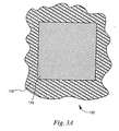
- FIGS. 3A to 3J and 4A to 4D A non-limiting exemplary method of fabricating an embodiment of the subject device 100 is provided in FIGS. 3A to 3J and 4A to 4D.
- the figures are not necessarily drawn to scale. For example, the diameter of the nanopore is exaggerated in order to make it visible at the drawing scale.
- fabrication of the subject device 100 includes producing a nanodimensioned passageway through a planar solid substrate, then positioning an electrode element about an opening of the passageway, wherein the electrode element includes first and second perimeter electrodes separated by an insulator element; and then positioning a proteinaceous channel in the nanodimensioned passageway to produce the nanopore.
- fabrication begins by forming in a substrate 118 a composite window 119 comprising a layer of silicon nitride typically 200 nm thick on top of a layer of silicon dioxide typically 500 nm thick, both layers forming a cladding layer on the exterior surfaces of a silicon wafer.
- the fabrication of this window 119 may be accomplished by the well-known steps of photolithography and etching of a hole in a silicon nitride layer on the bottom side of a substrate 118 such as a wafer of silicon, followed by etching of the substrate 118 in a hot aqueous caustic solution such as tetramethyl ammonium hydroxide (TMAH) in water.
- TMAH tetramethyl ammonium hydroxide
- the caustic etching process removes the silicon beneath the window 119 but leaves the silicon dioxide and silicon nitride layers, resulting in the layout structure illustrated in FIG. 3A.
- Window 119 as drawn is 40 micrometers ( ⁇ m) on a side, but may be larger or smaller.
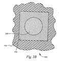
- a photolithography step is performed to open a window in photoresist, and the silicon nitride layer is etched away to leave silicon dioxide window 308 as illustrated in FIG. 4B.
- This etching step is performed using well-known plasma etching techniques employing carbon tetrafluoride (CF 4 ), oxygen, and nitrogen to achieve a much faster etch rate for silicon nitride than for silicon dioxide.
- CF 4 carbon tetrafluoride
- the technique of fabricating a silicon dioxide window region within a larger window region of silicon nitride on silicon dioxide is a separate invention, useful for obtaining a small, well-supported region of silicon dioxide with advantageous wetting properties as compared to silicon nitride.
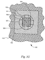
- FIB focused ion beam
- This FIB drilling process is followed by a published process of ion beam sculpting using a low energy beam of argon ions which acts to reduce the diameter of the edge of the nanoscale hole near proximate to the ion beam.
- This process is monitored by monitoring current of argon ions through the nanoscale hole, and is terminated when it has resulted in a nanodimensioned passageway 101 with a diameter ranging from about 10 nm to about 100 nm, as illustrated in FIG. 3C.
- FIG. 4A depicts an example of substrate 118 supporting multiple instances of oxide window 308 surrounding multiple instances of nanodimensioned passageways 101.
- Substrate 118 is tilted at an angle 201 so that its surface is, for example, 45 degrees from horizontal, and is rotated in a direction 202.
- Deposition source 203 is typically a vacuum evaporation source or a molecular beam epitaxy source or a sputtering source, and deposition stream 204 has some angular dispersion 205 as it travels along an average deposition path length 206.
- the result of the tilt and the rotation is that the deposited layer resulting from deposition stream 204 overhangs the edge of nanodimensioned passageway 101
- the thickness of the layer deposited as shown in FIG. 4A ranges from about 1 nm to about 10 nm, such as about 2 nm, and the deposited material is in some embodiments platinum.
- first peripheral electrode element 107 may range in width from about 2 ⁇ m to about 7 ⁇ m, such as about 4 ⁇ m to about 6 ⁇ m, including about 5 ⁇ m.
- a second angled line-of-sight deposition is performed as illustrated in FIG. 4B to form an insulating layer that will comprise insulator element 106.
- Angle 207 is less than angle 201, for example 35 degrees, and source 209 is typically a molecular beam epitaxy source or a sputtering source.
- the result of the deposition step of FIG. 4B is an insulator layer, in some embodiments comprising silicon dioxide.
- the insulating element 106 may range in thickness form about 1 nm to about 10 nm, including about 2 nm to about 9 nm, about 3 nm to about 8 nm, 4 nm to about 7 nm, such as about 5 nm to about 6 nm.
- the insulating element 106 overhangs the edge of nanopore 101 but which, as illustrated in FIGS. 1 and 2, does not occlude the overhanging perimeter the first perimeter electrode 107 because the perimeter of electrode element 107 is shadowed from the deposition stream during the line-of-sight deposition.
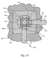
- a lithography step is performed and etching is performed in a dilute solution of buffered hydrofluouric acid called "buffered oxide etch" or "B.O.E," to define the lateral extent of optional insulator element 106 as shown in FIG. 3E.
- a photolithography step may be performed prior to the deposition step as illustrated in FIG. 4B and the optional insulator element 106 may be defined by means of a lift-off process.
- Second perimeter electrode 105 is similar to the fabrication of first perimeter electrode 107.
- the second perimeter electrode element ranges in thickness from about 1 nm to about 10 nm, such as about 2 nm to about 9 nm, including about 3 nm to about 8 nm, about 4 nm to about 7 nm, and 5 nm to about 6 nm a 2 nm thickness of platinum.
- the second perimeter element 105 will comprise platinum.
- the second perimeter electrode element 105 is formed by angled deposition as illustrated in FIG. 4C. Angle 210 is less than angle 207, for example 25 degrees, and source 212 is typically a vacuum evaporation source or a molecular beam epitaxy source or a sputtering source.
- the result of this deposition step is a layer in some embodiments 2 nm thick, and in some embodiments comprising platinum, which overhangs the edge of nanopore 101 as illustrated in FIGS. 1 and 2.
- Lithography and etching define the lateral extent of second perimeter electrode 105 as illustrated in FIG. 3F.
- a photolithography step may be performed prior to the deposition step as illustrated in FIG. 4C and the second perimeter electrode 105 may be defined by means of a lift-off process.
- the device further includes a second insulator element 104.
- Fabrication of second insulator element 104 is similar to fabrication of first insulator element 106.
- An insulating layer is formed by angled deposition as illustrated in FIG. 4D. Angle 213 is less than angle 210, for example 15 degrees.
- Source 215 is typically a molecular beam epitaxy source or a sputtering source. The result of this deposition step is a layer in some embodiments 2 nm thick, and in some embodiments comprising silicon dioxide, which overhangs the edge of nanopore 101 but which, as illustrated in FIGS.
- the lateral extent of optional second insulator element is defined by lithography and etching as illustrated in FIG. 3G.
- a photolithography step may be performed prior to the deposition step as illustrated in FIG. 4D and the second insulator element 104 may be defined by means of a lift-off process.
- electrical lead regions 120 and 121 are contacted to the first 107 and second 105 perimeter electrode regions at contact regions 123 and 122.
- Leads 120 and 121 are formed by standard IC techniques of metal deposition and lithography, for example by electron beam deposition of an aluminum layer followed by lithography and etching. Leads 120 and 121 may extend to contact pads, not shown, which provide for electrical contact to a circuit, not shown, similar to the circuit depicted for embodiment 100.
- an optional insulator layer 109 is formed, for example by spinning on a layer of a polyimide precursor and curing that precursor to form layer of polyimide insulator, in order to provide electrical insulation over leads 120 and 121 and over the ends of the first 107 and second 105 perimeter electrodes.
- the substrate 118 can then be diced by sawing to form individual nanopore chips, not shown, corresponding to substrate 108 as shown in FIG. 1 and FIG. 2.
- An individual nanopore chip can be connected to a fluidic apparatus to wet the first and second surfaces of the nanopore, and electrical connection of the chip to an electrical circuit can be performed.
- the next step in the fabrication process is to seal the nanodimensioned passageway with a lipid bilayer 103.
- a bristle of sufficient dimensions e.g. 10 to 200 ⁇ m diameter, usually 50 to 100 ⁇ m diameter
- a suitable lipid solution e.g. lipid in organic solvent, concentration range from about 1 to 5 mg per ml, usually from about 2 to 4 mg per ml.
- the dipped bristle is then gently brushed against the nanodimensioned passageway, which results in the formation of a lipid bilayer 103 that seals the nanodimensioned passageway (see FIG. 3J).
- the seal is then tested and the aperture may be brushed repeatedly with a clean bristle until a desired bilayer 103 is obtained.
- the final step in the preparation of the subject device is the insertion of the proteinaceous channel 102 into the lipid bilayer 103.
- an aqueous proteinaceous channel comprising solution is introduced into the first fluid containment member 110 and an electric field is applied across the lipid bilayer 103 in a manner sufficient for a proteinaceous channel 102 to insert or intercalate into the lipid bilayer 103.
- the above fabrication process produces a series of edges of nanopore 101 defining a portion of the nanopore with successively smaller diameters.
- the inner walls of the nanopore 101 will define a frustum configuration.
- Each edge has an overhanging region, which can also be called a cornice, the bottom side of which is shadowed from a subsequent line-of-sight deposition so that it remains free of deposits, or nearly so.
- the nanodimensioned passageway when first formed in window 308 has a fourth edge with a fourth portion of the nanopore 101 extending there through.
- the first perimeter electrode 107 overhangs the fourth edge, forming a third edge with a third portion of the nanopore 101 extending there through.
- the third portion of the nanopore is smaller than the fourth portion of the nanopore.
- the first insulator element 106 overhangs the third edge, forming a first insulator edge with a second portion of the nanopore extending there through.
- the second portion of the nanopore is smaller than the third portion of the nanopore.
- the second peripheral electrode 105 overhangs the first insulator element edge, forming a first electrode edge with a first portion of the nanopore being smaller than the second portion of the nanopore.
- the optional second insulator element 104 overhangs the second peripheral electrode 105 edge, forming an insulator edge with a portion of the nanopore smaller than the first portion of the nanopore.
- nanopore of initially large diameter and using the techniques of successive angled line-of-sight depositions, it is possible to end with a nanopore of small diameter.
- larger and smaller nanopores can be formed by varying the diameter of the edges, the thickness and number of deposited layers, and the angles of the successive depositions.
- the means of line-of-sight deposition chosen for any of the steps described above may result in some undesired deposition of insulator material onto electrode elements 107 or 105 or both, or may result in some undesired deposition of conductor material onto insulator regions 308, 106, or 104 or any combination of them.
- Such known techniques for removal include, but are not limited to, chemical etching, ion beam milling, sputtering, plasma etching, and reactive ion etching.
- the method of using the subject device 100 of the present invention includes applying an electrical voltage between the first 107 and second 105 perimeter electrodes of the device and monitoring the electrical current through the nanopore or monitoring the electrical current between first 107 and second 105 perimeter electrodes with an aim which may include detecting resonant tunneling current through a sample.
- the current flowing through the nanopore or sample is monitored and recorded over a period of time. Therefore, the monitoring provides a range of values representing the fluctuation of the current flowing through the nanopore.
- first 110 and second 111 fluid containment members of the device are filled with a conductive ionic aqueous solution.
- an electrical voltage may be applied between first 110 and second 111 fluid containment members.
- the monitoring of the electrical current through the nanopore or monitoring of the electrical current between first 107 and second 105 perimeter electrodes, or both, may be performed while a polymeric compound 112 is translocated through the proteinaceous channel 102 of the nanopore 101.
- the fluid sample may be placed in the first 110 fluid containment member and polymeric compound present in the sample translocates the nanopore.
- the polymeric compound 112 may comprise a variety of shapes, sizes and materials. The shape or size of the molecule is not important, but it must be capable of translocation through the proteinaceous channel 103 in the nanopore 101. For instance, both single stranded and double stranded RNA and DNA may be used as a polymeric compound 112. In addition, the polymeric compound 112 may contain groups or functional groups that are charged. Furthermore, metals or materials may be added, doped or intercalated within the polymeric compound 112 to provide a net dipole, a charge or allow for conductivity through the nanopre. The material of the polymeric compound 112 must allow for electron tunneling between electrodes.
- Polymeric compound 112 is schematically depicted as a string of beads that is threaded through the proteinaceous channel 102 of the nanopore 101.
- the polymeric compound 112 typically resides in an ionic solvent such as aqueous potassium chloride, not shown, which also extends through nanopore 101. It should be appreciated that, due to Brownian motion if nothing else, polymeric compound 112 is always in motion, and such motion will result in a time-varying position of each bead 113 within proteinaceous channel 102 of the nanopore 101.
- the motion of polymeric compound 112 will typically be biased in one direction or another through the pore by providing an external driving force, for example by establishing an electric field through the pore between a set of electrodes, not shown.
- the subject devices find use in a variety of different applications in which the ionic current through a nanopore is monitored or resonant tunneling current through a sample is monitored.
- Representative applications in which the subject devices find use include, for example, separation of molecules, capturing of molecules, characterization of polymeric compounds, e.g. the determining of the base sequence of a nucleic acid; and the like.
- the subject devices 100 of the present invention are useful in characterizing a polymeric compound 112, such as DNA.
- a polymeric compound 112 such as DNA.
- a single stranded nucleic acid may be translocated through the proteinaceous channel positioned in the nanopore and the effect of each base on the current flowing between first 107 and second 105 perimeter electrodes monitored and recorded, thereby providing a range of values representing the fluctuation of the current flowing between first 107 and second 105 perimeter electrodes as each monomeric unit 113 of the polymeric compound 112 translocates through the nanopore.
- Such a range of fluctuations over a period of time may then be analyzed to determine the identity of the monomeric units of the polymeric compound.
- the voltage generating element may be ramped, i.e., by application of a time-varying voltage, in order to provide a resonant tunneling current through a sample.
- the general principle is to ramp the tunneling voltage across the electrodes over the energy spectrum of the translocating polymeric compound. At specific voltages the incident energy will sequentially match the internal nucleotide energy levels, giving rise to a detectable change, e.g., increase, in the observed tunneling current.
- the ramp-time of the applied voltage is short compared to the nucleotide translocation time through the nanopore.
- the applied tunneling voltage frequency may be in excess of about 10 MHz.
- each type of monomer unit 113 has a characteristic internal energy level spectrum which would allow it to be distinguished from the other monomer unit 113 types.
- the applied voltage and tunneling current can be seen to produce a defined signal that is indicative of the portion of the biopolymer that is in a matched-barrier position between first 107 and second 105 perimeter electrodes.
- Each monomeric unit 113 of the polymeric compound 112 will produce a differing signal in the tunneling current over time as the varying voltage is applied. For instance, when each monomeric unit 113 or portion of the polymeric compound 112 is positioned such that the barriers are symmetric, a larger overall signal can be seen from the tunneling current as opposed to when the barriers are asymmetric.
- These differing signals provide a spectrum of the portion of the polymeric compound 112 that is positioned in a matched-barrier position between first 107 and second 105 perimeter electrodes.
- spectra can then be compared by computer to previous spectra or "finger prints" of nucleotides or portions of the polymeric compound 112 that have already been recorded, i.e., a reference or control.
- the residue of the polymeric compound 112 can then be determined by comparison to this reference or control, e.g., that may be in the form of a database.
- This data and information can then be stored and supplied as output data of a final sequence.
- the base sequence of the nucleic acid can be determined.
- Methods of characterizing polymeric molecules in this manner are further described in application Ser. No. 08/405,735 and entitled Characterization of Individual Polymer Molecules Based on Monomer-interface Interactions, the disclosure of which is herein incorporated by reference.
- Results obtained from such methods may be raw results, such as signal lines for the signal producing system of the device.
- the results may be processed results, such as those obtained by subtracting a background measurement, or an indication of the identity of a particular residue of a polymeric compound (for example an indication of a particular nucleotide or amino acid.
- the subject methods also include a step of transmitting data or results from the monitoring step, as described above, to a remote location.
- a remote location is meant a location other than the location at which the translocation occurs.
- a remote location could be another location (e.g. office, lab, etc.) in the same city, another location in a different city, another location in a different state, another location in a different country, etc.
- office, lab, etc. e.g. office, lab, etc.
- the two items are at least in different buildings, and may be at least one mile, ten miles, or at least one hundred miles apart.
Applications Claiming Priority (1)
| Application Number | Priority Date | Filing Date | Title |
|---|---|---|---|
| US11/107,461 US20060231419A1 (en) | 2005-04-15 | 2005-04-15 | Molecular resonant tunneling sensor and methods of fabricating and using the same |
Publications (2)
| Publication Number | Publication Date |
|---|---|
| EP1712891A2 true EP1712891A2 (de) | 2006-10-18 |
| EP1712891A3 EP1712891A3 (de) | 2006-12-06 |
Family
ID=36607487
Family Applications (1)
| Application Number | Title | Priority Date | Filing Date |
|---|---|---|---|
| EP05020589A Withdrawn EP1712891A3 (de) | 2005-04-15 | 2005-09-21 | Molekulärer Sensor mit resonantem Tunneleffekt und dessen Herstellungs- und Anwendungsverfahren. |
Country Status (2)
| Country | Link |
|---|---|
| US (1) | US20060231419A1 (de) |
| EP (1) | EP1712891A3 (de) |
Cited By (12)
| Publication number | Priority date | Publication date | Assignee | Title |
|---|---|---|---|---|
| WO2013151532A1 (en) * | 2012-04-02 | 2013-10-10 | Lux Bio Group, Inc. | Apparatus and method for molecular separation, purification, and sensing |
| CN105273991A (zh) * | 2010-02-08 | 2016-01-27 | 吉尼亚科技公司 | 用于在纳米孔中操作分子的系统和方法 |
| US9434990B2 (en) | 2012-04-02 | 2016-09-06 | Lux Bio Group, Inc. | Apparatus and method for molecular separation, purification, and sensing |
| WO2017036962A1 (en) * | 2015-08-31 | 2017-03-09 | Genia Technologies, Inc. | Small aperture large electrode nanopore cell and method of manufacture |
| US9678055B2 (en) | 2010-02-08 | 2017-06-13 | Genia Technologies, Inc. | Methods for forming a nanopore in a lipid bilayer |
| USRE46479E1 (en) | 2006-09-21 | 2017-07-18 | Los Alamos National Security, Llc | Electrochemical detection of single molecules using abiotic nanopores having electrically tunable dimensions |
| US9732384B2 (en) | 2012-04-02 | 2017-08-15 | Lux Bio Group, Inc. | Apparatus and method for molecular separation, purification, and sensing |
| US9759711B2 (en) | 2013-02-05 | 2017-09-12 | Genia Technologies, Inc. | Nanopore arrays |
| US9869655B2 (en) | 2011-01-24 | 2018-01-16 | Genia Technologies, Inc. | System for detecting electrical properties of a molecular complex |
| US10036725B2 (en) | 2013-10-17 | 2018-07-31 | Genia Technologies, Inc. | Non-faradaic, capacitively coupled measurement in a nanopore cell array |
| US10036739B2 (en) | 2015-01-27 | 2018-07-31 | Genia Technologies, Inc. | Adjustable bilayer capacitance structure for biomedical devices |
| US10724987B2 (en) | 2012-02-27 | 2020-07-28 | Roche Sequencing Solutions, Inc. | Sensor circuit for controlling, detecting, and measuring a molecular complex |
Families Citing this family (34)
| Publication number | Priority date | Publication date | Assignee | Title |
|---|---|---|---|---|
| US8906609B1 (en) | 2005-09-26 | 2014-12-09 | Arrowhead Center, Inc. | Label-free biomolecule sensor based on surface charge modulated ionic conductance |
| US20080079442A1 (en) * | 2006-08-31 | 2008-04-03 | Joshua Posamentier | Quantum tunneling biometric identification methods and apparatuses |
| WO2008124706A2 (en) | 2007-04-06 | 2008-10-16 | Arizona Board Of Regents Acting For And On Behalf Of Arizona State University | Devices and methods for target molecule characterization |
| EP3543357A1 (de) | 2007-05-08 | 2019-09-25 | Trustees of Boston University | Chemische funktionalisierung von festkörpernanoporen und nanoporenarrays und anwendungen davon |
| WO2010117470A2 (en) | 2009-04-10 | 2010-10-14 | Pacific Biosciences Of California, Inc. | Nanopore sequencing devices and methods |
| US9017937B1 (en) | 2009-04-10 | 2015-04-28 | Pacific Biosciences Of California, Inc. | Nanopore sequencing using ratiometric impedance |
| US8926904B2 (en) | 2009-05-12 | 2015-01-06 | Daniel Wai-Cheong So | Method and apparatus for the analysis and identification of molecules |
| EP2483680A4 (de) | 2009-09-30 | 2014-01-01 | Quantapore Inc | Ultraschnelle sequenzierung biologischer polymere mithilfe einer markierten nanopore |
| CN101694474B (zh) * | 2009-10-22 | 2012-10-10 | 浙江大学 | 一种纳米孔电学传感器 |
| US8652779B2 (en) | 2010-04-09 | 2014-02-18 | Pacific Biosciences Of California, Inc. | Nanopore sequencing using charge blockade labels |
| KR101648417B1 (ko) * | 2010-05-14 | 2016-08-16 | 서울대학교산학협력단 | 절연된 박막 전극의 전위 측정을 통한 나노포어 입자 검출기 |
| CN102795596B (zh) * | 2011-05-27 | 2014-12-10 | 中国科学院物理研究所 | 超小2nm直径金属纳米孔的超快激光脉冲法制备 |
| EP2737536B1 (de) * | 2011-07-27 | 2018-05-09 | The Board of Trustees of the University of Illionis | Nanopore-sensoren für biomolekulare charakterisierung |
| BR112014003911A2 (pt) | 2011-08-19 | 2017-03-14 | Synthetic Genomics Inc | método integrado para a identificação de alto rendimento de novas composições pesticidas e seu uso |
| US20140231274A1 (en) * | 2011-11-22 | 2014-08-21 | Panasonic Corporation | Single molecule detection method and single molecule detection apparatus for biological molecule, and disease marker testing apparatus |
| US9651539B2 (en) | 2012-10-28 | 2017-05-16 | Quantapore, Inc. | Reducing background fluorescence in MEMS materials by low energy ion beam treatment |
| US20150346188A1 (en) * | 2012-12-21 | 2015-12-03 | Ibis Biosciences, Inc. | Stabilized nanopore and micropore structures and methods for making and using the same |
| US9791453B2 (en) | 2012-12-26 | 2017-10-17 | International Business Machines Corporation | Methods for determining binding capability of target ligands with G protein-coupled receptors using translocation through nanochannels |
| US9250206B2 (en) * | 2013-04-04 | 2016-02-02 | International Business Machines Corporation | Controlled translocation of macromolecules employing a funnel nanopore structure and a gel |
| CN105283560B (zh) | 2013-05-24 | 2018-11-30 | 昆塔波尔公司 | 基于纳米孔的通过混合的fret检测的核酸分析 |
| US9255321B2 (en) * | 2013-10-15 | 2016-02-09 | Globalfoundries Inc. | Directed surface functionalization on selected surface areas of topographical features with nanometer resolution |
| US10024851B2 (en) | 2013-10-15 | 2018-07-17 | International Business Machines Corporation | Use of disulfide bonds to form a reversible and reusable coating for nanofluidic devices |
| US9303310B2 (en) * | 2013-10-15 | 2016-04-05 | International Business Machines Corporation | Nanofluidic sensor comprising spatially separated functional sensing components |
| US10145846B2 (en) * | 2014-04-16 | 2018-12-04 | Arizona Board Of Regents On Behalf Of Arizona State University | Digital protein sensing chip and methods for detection of low concentrations of molecules |
| US9921181B2 (en) | 2014-06-26 | 2018-03-20 | International Business Machines Corporation | Detection of translocation events using graphene-based nanopore assemblies |
| EP3702780B1 (de) * | 2014-07-31 | 2022-03-02 | Illumina, Inc. | Hybride nanoporensensoren |
| CN107109472B (zh) | 2014-10-10 | 2021-05-11 | 昆塔波尔公司 | 利用互相猝灭的荧光标记物的基于纳米孔的聚合物分析 |
| JP6757316B2 (ja) | 2014-10-24 | 2020-09-16 | クアンタポール, インコーポレイテッド | ナノ構造のアレイを使用するポリマーの効率的光学分析 |
| GB201510322D0 (en) * | 2015-06-12 | 2015-07-29 | Imp Innovations Ltd | Apparatus and method |
| EP3482196B1 (de) | 2016-07-05 | 2022-02-23 | Quantapore, Inc. | Optisch basierte nanoporensequenzierung |
| EP3519097A4 (de) | 2016-10-03 | 2020-04-29 | Genvida Technology Company Limited | Verfahren und vorrichtung für die analyse und identifizierung von molekülen |
| JP7234224B2 (ja) * | 2017-10-02 | 2023-03-07 | ザ リージェンツ オブ ザ ユニヴァーシティ オブ カリフォルニア | 標的分子をナノポアに送達するシステム及び方法 |
| US11143618B2 (en) * | 2018-04-09 | 2021-10-12 | Roche Sequencing Solutions, Inc. | Fabrication of tunneling junctions with nanopores for molecular recognition |
| GB202016874D0 (en) * | 2020-10-23 | 2020-12-09 | Oxford Nanopore Tech Ltd | Nanopore support structure and manufacture thereof |
Citations (4)
| Publication number | Priority date | Publication date | Assignee | Title |
|---|---|---|---|---|
| WO2000079257A1 (en) * | 1999-06-22 | 2000-12-28 | President And Fellows Of Harvard College | Molecular and atomic scale evaluation of biopolymers |
| DE19936302A1 (de) * | 1999-08-02 | 2001-02-15 | Niels Fertig | Vorrichtungen und Verfahren zur Untersuchung von Ionenkanälen in Membranen |
| WO2004035211A1 (en) * | 2002-10-15 | 2004-04-29 | Advanced Research Corporation | Solid state membrane channel device for the measurement and characterization of atomic and molecular sized samples |
| EP1486775A1 (de) * | 2003-06-12 | 2004-12-15 | Agilent Technologies, Inc. (a Delaware Corporation) | Nanopore mit Resonanztunnelelektroden |
Family Cites Families (14)
| Publication number | Priority date | Publication date | Assignee | Title |
|---|---|---|---|---|
| US6362002B1 (en) * | 1995-03-17 | 2002-03-26 | President And Fellows Of Harvard College | Characterization of individual polymer molecules based on monomer-interface interactions |
| US5795782A (en) * | 1995-03-17 | 1998-08-18 | President & Fellows Of Harvard College | Characterization of individual polymer molecules based on monomer-interface interactions |
| US6267872B1 (en) * | 1998-11-06 | 2001-07-31 | The Regents Of The University Of California | Miniature support for thin films containing single channels or nanopores and methods for using same |
| US6464842B1 (en) * | 1999-06-22 | 2002-10-15 | President And Fellows Of Harvard College | Control of solid state dimensional features |
| US6783643B2 (en) * | 1999-06-22 | 2004-08-31 | President And Fellows Of Harvard College | Control of solid state dimensional features |
| AU6020400A (en) * | 1999-07-21 | 2001-02-05 | Hitachi Maxell, Ltd. | Read/write head and magnetic recording device |
| US20030104428A1 (en) * | 2001-06-21 | 2003-06-05 | President And Fellows Of Harvard College | Method for characterization of nucleic acid molecules |
| US6706203B2 (en) * | 2001-10-30 | 2004-03-16 | Agilent Technologies, Inc. | Adjustable nanopore, nanotome, and nanotweezer |
| US6706204B2 (en) * | 2001-12-19 | 2004-03-16 | Agilent Technologies, Inc. | Method of fabricating and a device that includes nanosize pores having well controlled geometries |
| US7347921B2 (en) * | 2003-07-17 | 2008-03-25 | Agilent Technologies, Inc. | Apparatus and method for threading a biopolymer through a nanopore |
| US6843281B1 (en) * | 2003-07-30 | 2005-01-18 | Agilent Techinologies, Inc. | Methods and apparatus for introducing liquids into microfluidic chambers |
| US20050069687A1 (en) * | 2003-09-25 | 2005-03-31 | Barth Phillip W. | Apparatus and method for making a tensile diaphragm with a compressive region |
| US7138672B2 (en) * | 2003-09-25 | 2006-11-21 | Agilent Technologies, Inc. | Apparatus and method for making a tensile diaphragm with an insert |
| US6846702B1 (en) * | 2003-10-24 | 2005-01-25 | Agilent Technologies, Inc. | Nanopore chip with N-type semiconductor |
-
2005
- 2005-04-15 US US11/107,461 patent/US20060231419A1/en not_active Abandoned
- 2005-09-21 EP EP05020589A patent/EP1712891A3/de not_active Withdrawn
Patent Citations (4)
| Publication number | Priority date | Publication date | Assignee | Title |
|---|---|---|---|---|
| WO2000079257A1 (en) * | 1999-06-22 | 2000-12-28 | President And Fellows Of Harvard College | Molecular and atomic scale evaluation of biopolymers |
| DE19936302A1 (de) * | 1999-08-02 | 2001-02-15 | Niels Fertig | Vorrichtungen und Verfahren zur Untersuchung von Ionenkanälen in Membranen |
| WO2004035211A1 (en) * | 2002-10-15 | 2004-04-29 | Advanced Research Corporation | Solid state membrane channel device for the measurement and characterization of atomic and molecular sized samples |
| EP1486775A1 (de) * | 2003-06-12 | 2004-12-15 | Agilent Technologies, Inc. (a Delaware Corporation) | Nanopore mit Resonanztunnelelektroden |
Non-Patent Citations (1)
| Title |
|---|
| BRANTON D: "Nanopore transducers: prospects for single molecule electrophoresis" TRANSDUCERS, SOLID-STATE SENSORS, ACTUATORS AND MICROSYSTEMS, 12TH INNATIONAL CONFERENCE ON, 2003, PISCATAWAY, NJ, USA,IEEE, vol. 1, 9 June 2003 (2003-06-09), pages 210-213, XP010646506 ISBN: 0-7803-7731-1 * |
Cited By (32)
| Publication number | Priority date | Publication date | Assignee | Title |
|---|---|---|---|---|
| USRE46479E1 (en) | 2006-09-21 | 2017-07-18 | Los Alamos National Security, Llc | Electrochemical detection of single molecules using abiotic nanopores having electrically tunable dimensions |
| USRE46594E1 (en) | 2006-09-21 | 2017-10-31 | Los Alamos National Security, Llc | Electrochemical detection of single molecules using abiotic nanopores having electrically tunable dimensions |
| USRE46545E1 (en) | 2006-09-21 | 2017-09-12 | Los Alamos National Security, Llc | Electrochemical detection of single molecules using abiotic nanopores having electrically tunable dimensions |
| CN105273991A (zh) * | 2010-02-08 | 2016-01-27 | 吉尼亚科技公司 | 用于在纳米孔中操作分子的系统和方法 |
| EP2534284A4 (de) * | 2010-02-08 | 2017-01-25 | Genia Technologies Inc. | Systeme und verfahren zur manipulation eines moleküls in einer nanopore |
| US10371692B2 (en) | 2010-02-08 | 2019-08-06 | Genia Technologies, Inc. | Systems for forming a nanopore in a lipid bilayer |
| CN105273991B (zh) * | 2010-02-08 | 2019-05-10 | 吉尼亚科技公司 | 用于在纳米孔中操作分子的系统和方法 |
| US9678055B2 (en) | 2010-02-08 | 2017-06-13 | Genia Technologies, Inc. | Methods for forming a nanopore in a lipid bilayer |
| US10330633B2 (en) | 2011-01-24 | 2019-06-25 | Genia Technologies, Inc. | System for communicating information from an array of sensors |
| US9869655B2 (en) | 2011-01-24 | 2018-01-16 | Genia Technologies, Inc. | System for detecting electrical properties of a molecular complex |
| US10156541B2 (en) | 2011-01-24 | 2018-12-18 | Genia Technologies, Inc. | System for detecting electrical properties of a molecular complex |
| US10724987B2 (en) | 2012-02-27 | 2020-07-28 | Roche Sequencing Solutions, Inc. | Sensor circuit for controlling, detecting, and measuring a molecular complex |
| US11275052B2 (en) | 2012-02-27 | 2022-03-15 | Roche Sequencing Solutions, Inc. | Sensor circuit for controlling, detecting, and measuring a molecular complex |
| US10422000B2 (en) | 2012-04-02 | 2019-09-24 | Lux Bio Group Inc. | Apparatus and method for molecular separation, purification, and sensing |
| US9632073B2 (en) | 2012-04-02 | 2017-04-25 | Lux Bio Group, Inc. | Apparatus and method for molecular separation, purification, and sensing |
| US8968545B2 (en) | 2012-04-02 | 2015-03-03 | Lux Bio Group, Inc. | Apparatus and method for molecular separation, purification, and sensing |
| US9434990B2 (en) | 2012-04-02 | 2016-09-06 | Lux Bio Group, Inc. | Apparatus and method for molecular separation, purification, and sensing |
| WO2013151532A1 (en) * | 2012-04-02 | 2013-10-10 | Lux Bio Group, Inc. | Apparatus and method for molecular separation, purification, and sensing |
| US10175223B2 (en) | 2012-04-02 | 2019-01-08 | Lux Bio Group, Inc. | Apparatus and method for molecular separation, purification, and sensing |
| US9732384B2 (en) | 2012-04-02 | 2017-08-15 | Lux Bio Group, Inc. | Apparatus and method for molecular separation, purification, and sensing |
| US9759711B2 (en) | 2013-02-05 | 2017-09-12 | Genia Technologies, Inc. | Nanopore arrays |
| US10012637B2 (en) | 2013-02-05 | 2018-07-03 | Genia Technologies, Inc. | Nanopore arrays |
| US10809244B2 (en) | 2013-02-05 | 2020-10-20 | Roche Sequencing Solutions, Inc. | Nanopore arrays |
| US10393700B2 (en) | 2013-10-17 | 2019-08-27 | Roche Sequencing Solutions, Inc. | Non-faradaic, capacitively coupled measurement in a nanopore cell array |
| US10036725B2 (en) | 2013-10-17 | 2018-07-31 | Genia Technologies, Inc. | Non-faradaic, capacitively coupled measurement in a nanopore cell array |
| US10345290B2 (en) | 2015-01-27 | 2019-07-09 | Genia Technologies, Inc. | Adjustable bilayer capacitance structure for biomedical devices |
| US10976302B2 (en) | 2015-01-27 | 2021-04-13 | Roche Sequencing Solutions, Inc. | Adjustable bilayer capacitance structure for biomedical devices |
| US10036739B2 (en) | 2015-01-27 | 2018-07-31 | Genia Technologies, Inc. | Adjustable bilayer capacitance structure for biomedical devices |
| WO2017036962A1 (en) * | 2015-08-31 | 2017-03-09 | Genia Technologies, Inc. | Small aperture large electrode nanopore cell and method of manufacture |
| US10809243B2 (en) | 2015-08-31 | 2020-10-20 | Roche Sequencing Solutions, Inc. | Small aperture large electrode cell |
| US11346836B2 (en) | 2015-08-31 | 2022-05-31 | Roche Sequencing Solutions, Inc. | Small aperture large electrode cell |
| US11740227B2 (en) | 2015-08-31 | 2023-08-29 | Roche Sequencing Solutions, Inc. | Small aperture large electrode cell |
Also Published As
| Publication number | Publication date |
|---|---|
| US20060231419A1 (en) | 2006-10-19 |
| EP1712891A3 (de) | 2006-12-06 |
Similar Documents
| Publication | Publication Date | Title |
|---|---|---|
| EP1712891A2 (de) | Molekulärer Sensor mit resonantem Tunneleffekt und dessen Herstellungs- und Anwendungsverfahren. | |
| EP1486775A1 (de) | Nanopore mit Resonanztunnelelektroden | |
| US11946925B2 (en) | Nanopore sensor having a fluidic passage for local electrical potential measurement | |
| US20210341459A1 (en) | Nanopore-containing substrates with aligned nanoscale electronic elements and methods of making and using same | |
| US7777505B2 (en) | Nanopore platforms for ion channel recordings and single molecule detection and analysis | |
| US20190317072A1 (en) | Systems and devices for molecule sensing and method of manufacturing thereof | |
| Pang et al. | Fixed-gap tunnel junction for reading DNA nucleotides | |
| CN103718029B (zh) | 纳米孔式分析装置 | |
| US8860438B2 (en) | Electrical double layer capacitive devices and methods of using same for sequencing polymers and detecting analytes | |
| US20090215156A1 (en) | Method for Fabricating Nanogap and Nanogap Sensor | |
| US20070218471A1 (en) | Method and device for detecting dna using surface-treated nanopore | |
| JP2003533676A (ja) | 超高速の核酸配列決定のための電界効果トランジスタ装置 | |
| US20170038369A1 (en) | Digital protein sensing chip and methods for detection of low concentrations of molecules | |
| EP1643235A1 (de) | Biopolymer-Resonanztunneln mit einer Gatterspannungsquelle | |
| US20060071209A1 (en) | Biopolymer resonant tunneling with a gate voltage source | |
| CN110192096A (zh) | 生物体物质检测用设备和检测装置、离子电流的测定方法以及生物体物质的识别方法 | |
| Tsutsui et al. | Transverse field effects on DNA-sized particle dynamics | |
| US7114378B1 (en) | Planar resonant tunneling sensor and method of fabricating and using the same | |
| US20220260550A1 (en) | Sequencing of Biopolymers By Motion-Controlled Electron Tunneling | |
| US20230038666A1 (en) | Nanobridge biosensor and memory array | |
| US10962535B2 (en) | Porous material functionalized nanopore for molecular sensing apparatus |
Legal Events
| Date | Code | Title | Description |
|---|---|---|---|
| PUAI | Public reference made under article 153(3) epc to a published international application that has entered the european phase |
Free format text: ORIGINAL CODE: 0009012 |
|
| AK | Designated contracting states |
Kind code of ref document: A2 Designated state(s): AT BE BG CH CY CZ DE DK EE ES FI FR GB GR HU IE IS IT LI LT LU LV MC NL PL PT RO SE SI SK TR |
|
| AX | Request for extension of the european patent |
Extension state: AL BA HR MK YU |
|
| PUAL | Search report despatched |
Free format text: ORIGINAL CODE: 0009013 |
|
| AK | Designated contracting states |
Kind code of ref document: A3 Designated state(s): AT BE BG CH CY CZ DE DK EE ES FI FR GB GR HU IE IS IT LI LT LU LV MC NL PL PT RO SE SI SK TR |
|
| AX | Request for extension of the european patent |
Extension state: AL BA HR MK YU |
|
| RIC1 | Information provided on ipc code assigned before grant |
Ipc: G01N 27/416 20060101ALI20061030BHEP Ipc: C12Q 1/68 20060101ALI20061030BHEP Ipc: G01N 15/10 20060101AFI20061030BHEP |
|
| RAP1 | Party data changed (applicant data changed or rights of an application transferred) |
Owner name: AGILENT TECHNOLOGIES, INC. |
|
| 17P | Request for examination filed |
Effective date: 20070605 |
|
| AKX | Designation fees paid |
Designated state(s): DE FR GB |
|
| 17Q | First examination report despatched |
Effective date: 20090514 |
|
| STAA | Information on the status of an ep patent application or granted ep patent |
Free format text: STATUS: THE APPLICATION IS DEEMED TO BE WITHDRAWN |
|
| 18D | Application deemed to be withdrawn |
Effective date: 20090925 |