EP1708262A2 - Thermischer Leiter und dessen Verwendung - Google Patents
Thermischer Leiter und dessen Verwendung Download PDFInfo
- Publication number
- EP1708262A2 EP1708262A2 EP06075616A EP06075616A EP1708262A2 EP 1708262 A2 EP1708262 A2 EP 1708262A2 EP 06075616 A EP06075616 A EP 06075616A EP 06075616 A EP06075616 A EP 06075616A EP 1708262 A2 EP1708262 A2 EP 1708262A2
- Authority
- EP
- European Patent Office
- Prior art keywords
- thermal
- integrated circuit
- thermal transfer
- transfer device
- thermal conductor
- Prior art date
- Legal status (The legal status is an assumption and is not a legal conclusion. Google has not performed a legal analysis and makes no representation as to the accuracy of the status listed.)
- Withdrawn
Links
Images



Classifications
-
- H—ELECTRICITY
- H10—SEMICONDUCTOR DEVICES; ELECTRIC SOLID-STATE DEVICES NOT OTHERWISE PROVIDED FOR
- H10W—GENERIC PACKAGES, INTERCONNECTIONS, CONNECTORS OR OTHER CONSTRUCTIONAL DETAILS OF DEVICES COVERED BY CLASS H10
- H10W40/00—Arrangements for thermal protection or thermal control
- H10W40/70—Fillings or auxiliary members in containers or in encapsulations for thermal protection or control
- H10W40/77—Auxiliary members characterised by their shape
- H10W40/774—Pistons, e.g. spring-loaded members
Definitions
- Integrated circuits and other electronic devices generate heat when used. Heat dissipation techniques are often employed to prevent the temperature of the electronic devices from exceeding the manufacturer's temperature limit specifications. The life expectancy of electronic devices is significantly shortened if they are operated at temperatures that exceed the manufacturer's specifications. Thus, it is advantageous to transfer heat that is generated from active surfaces of electronic devices away from the devices. In one example, heat may be removed from a junction formed between an integrated circuit electrically attached to a substrate.
- Integrated circuit is the formal term for a the square of silicon containing a circuit
- the substrate is the surface or board on which the integrated circuits are mounted.
- the substrate may have multiple layers for the interconnection of the integrated circuits.
- a high efficiency thermal path is conventionally used and thermally attached thereto.
- One technique for transferring the heat away from the junction is to place the high efficiency thermal path between the junction and a thermal dissipating device, such as a heat sink.
- a thermal dissipating device such as a heat sink.
- the use of a high efficiency thermal conductor enhances the thermal path for the heat to travel through and subsequently transfer to some other medium, such as air, liquid or other form of material away from the junction.
- the material used to dissipate this heat generally has a substantially high thermal conductivity that is at least sufficient to maintain an acceptable temperature on or across the electronic device.
- one embodiment of the invention is directed to a thermal conductor suitable for communicating heat from an integrated circuit to a thermal transfer device.
- the thermal conductor comprises a base having a first portion and a second portion, wherein the first portion is adapted to be positioned proximate the integrated circuit, and further wherein the second portion includes sidewalls that define an aperture in the body and forms a spherical cavity, and wherein the aperture is adapted to receive at least a portion of the thermal transfer device such that at least a portion of the thermal transfer device is in thermal communication with the integrated circuit
- the thermal transfer assembly 10 includes a substrate 12, an integrated circuit 14, a thermal conductor 16, a thermal transfer device 18, and a thermal dissipating device 20.
- a biasing device 21 is further included and is inserted between at least a portion of the thermal transfer device 18 and at least a portion of the thermal dissipating device 20.
- the thermal transfer assembly 10 may be used in various types of electronic devices.
- the thermal transfer assembly 10 is thermally coupled to a junction formed between the integrated circuit 14 electrically connected to the substrate 12.
- the thermal transfer assembly 10 is not limited to the junction between the substrate 12 and the integrated circuit 14, and, therefore, the thermal transfer assembly 10 may be thermally coupled at any point along the substrate 12 or the integrated circuit 14.
- the substrate 12 is a board on which at least one integrated circuit 14 is electrically mounted.
- the substrate 12 is optionally formed from silicon, ceramic, or the like and is in the form of a multilayered printed board (not shown) on which multiple integrated circuits 14 may be mounted and through which all interconnections therebetween may be made.
- the thermal transfer assembly 10 provides a direct thermal path from at least one integrated circuit 14 to the thermal dissipating device 20.
- the substrate 12 may instead be made of fiberglass or a combination of materials.
- One of ordinary skill in the art will recognize the various materials that may be incorporated into the substrate 12. The principles of the thermal transfer assembly 10 may be incorporated into all of such substrates 12.
- the integrated circuit 14 is a semiconductor component.
- the integrated circuit 14 may be electrically mounted to the substrate 12 with solder or using other techniques known in the art.
- Fig. 1 illustrates a single integrated circuit 14 and thermal transfer assembly 10, multiple integrated circuits 14, such as those illustrated in Figs 3-5, in addition to other embodiments of thermal transfer assemblies may, similarly, be implemented in accordance with the invention.
- the thermal conductor 16 includes a first region 22 and a second region 24.
- the first region 22 is proximate to the integrated circuit 14 and the second region 24 is proximate to the thermal transfer device 18.
- the thermal conductor 16 extends beyond the integrated circuit 14 in one common dimension.
- Fig. 1 illustrates, one way to achieve this is to provide the first region 22 having a side in one dimension that is larger than the perimeter of the integrated circuit 14 in the same dimension.
- the first region 22 is larger than the integrated circuit 14 in all dimensions.
- Fig. 2 highlights the thermal connection between the thermal transfer device 18 and the integrated circuit 14. Although the thermal transfer device 18 appears to physically contact the integrated circuit 14 this is not a necessary feature of the invention. Thus, thermal communication may be achieved both through physical and non-physical contact between the thermal transfer device 18 and the integrated circuit 14. However, physical contact is maintained between the thermal conductor 16 and the thermal transfer device 18.
- the first region 22 maintains a relationship with the integrated circuit 14 using a combination of thermal interface material (not shown) and a biasing force exerted from the thermal transfer device 18 upon the thermal conductor 16.
- the biasing force originates from the relationship between the biasing device 21, the thermal dissipating device 20 and the thermal transfer device 18.
- the thermal interface material may be used to eliminate any air gaps that may increase the thermal resistance between the junction.
- the thermal interface material is generally known and used by those of ordinary skill in the art and will readily recognized by such. It should also be noted that the invention contemplates that the thermal interface material may be used at any region of the thermal transfer assembly 10.
- the second region 24 of the thermal conductor 16 includes sidewalls that define an aperture 26.
- the aperture 26 extends into the first region 22 such that at least a portion of thermal transfer device 18 is thermally coupled with at least a portion of the integrated circuit 14 and the thermal conductor 16 when the thermal transfer assembly 10 is fully constructed.
- a first diameter of the aperture 26 is equal to, or larger than, a diameter of the thermal transfer device 18 and tapers down to a second diameter that is still larger than the diameter of the thermal transfer device 18 yet smaller than the first diameter.
- the first and second diameters of the aperture 26 may be of a uniform size, and further, the uniform diameter may be any size that allows the thermal transfer device 18 entry into the aperture 26 to thermally couple with the integrated circuit 14.
- the aperture 26 of the thermal conductor 16 forms a spherical cavity.
- the thermal transfer device 18 is substantially guided thereby. This feature aids in the proper alignment and orientation of the thermal dissipating device 20 with the substrate 12 and substantially eliminates the need to maintain strict tolerances while attaching the thermal dissipating device 20 to the integrated circuit 14 and the substrate 12.
- the thermal transfer device 18 includes a convex spherical end that corresponds with the spherical cavity of the thermal conductor 16 and may be received thereby. This relationship provides a pivot interface between the thermal conductor 16 and the thermal transfer device 18 such that the thermal conductor 16 is guided into substantial planar alignment with the integrated circuit 14 when force is added thereto from the thermal transfer device 18. It is noted that this planar alignment is independent of the orientation of the thermal transfer device 18. That is, bringing the thermal conductor 16 and the integrated circuit 14 into substantial planar alignment substantially minimizes the air gaps that may arise therebetween and increases the thermal transfer efficiency more surface area of the integrated circuit 14 is covered by the thermal conductor 16.
- the thermal transfer device 18 includes an evaporator region 28 and a condenser region 30.
- the evaporator region 28 is configured to thermally communicate with at least a portion of the integrated circuit 14 and least a portion of the aperture 26.
- at least a portion of the evaporator region 28 is spherical to correspond with at least a portion of the spherical cavity of the aperture 26. That is, as the evaporation region 28 of the thermal transfer device 18 contacts the aperture 26, the thermal conductor 16 pivots to substantially maximize its coverage across the integrated circuit 14 so that the integrated circuit 14 and the thermal conductor 16 are substantially planar. This relationship not only substantially correctly aligns the thermal dissipating device 20 with the integrated circuit 14 and the substrate 12, but also substantially aligns the thermal conductor 16 with the integrated circuit 14.
- the spherical engagement between the thermal transfer device 18 and the spherical cavity formed within aperture 26 may result in movement of one of the substrate 12, the thermal dissipating device 20, or both so that they are substantially brought into alignment if they are not already aligned.
- the substantial alignment of these structures also helps to substantially ensure that the thermal communication between the integrated circuit 14 and the thermal conductor 16 is additionally substantially planar therebetween.
- the thermal transfer device 18 is a thermally conductive pin 32.
- thermal transfer device 18 is a thermally conductive pipe 34.
- the thermally conductive pin 32 and the thermally conductive pipe 34 are solid.
- the thermally conductive pin 34 and the thermally conductive pipe 34 may instead be a tubular device having a hollow inner portion that holds a liquid such as water, or acetone in a vacuum.
- an inner surface of the thermal pipe 34 is lined with a porous material that acts as a wick.
- thermal dissipating device 20 is fabricated from aluminum.
- Aluminum is used as it has good thermal conducting properties. It should be noted, however, that other types of materials having a high degree of thermal conductivity may alternatively be used and the invention should not be limited to such. Also, well known thermally conductive plating can be placed on the surface of the thermal transfer device 18, or thermal conduct 16 to enhance thermal conductivity therebetween.
- thermal dissipating device 20 includes a base portion 36 having at least two pedestals 36 that define an aperture 38 therebetween.
- the aperture 38 is adapted to receive at least a portion of the condenser region 30 of the thermal transfer device 18.
- thermal interface material may be disposed at least between thermal transfer device 18 and aperture 38 as there is often a large number of microscopic gaps.
- the thermal interface material may also provide a lubricous interface between the pedestals 36 and the thermal transfer device 18. The thermal interface material the two surfaces transfer heat between two structures more effectively.
- a biasing device 21 is integrated between the condenser region 30 of thermal transfer device 18 and a floor 40 of aperture 38. Biasing device 21 maintains pressure between evaporator end 28 of thermal transfer device 18 and aperture 26 of thermal conductor 16. In this manner, and as illustrated in Fig. 4, the biasing device 21 at least compensates for any elevation variation of the thermal assembly 10 and substantially ensures a planar relationship between the integrated circuit 14 and the thermal conductor 16. The biasing device 21 also prevents overstressing of integrated circuit 14 if too much pressure is applied along any point of the thermal dissipating device 20 or the substrate 12 and the integrated circuit 14. As previously mentioned above, a lubricous interface is applied between aperture 38 and thermal transfer device 18 to at least provide a sliding relationship therebetween so that the biasing device 21 may effectively control the pressure.
- biasing device 21 is a coil spring 42. In another embodiment, biasing device is an elastomeric material. The feature and advantages of each will be further discussed hereinbelow.
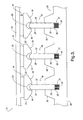
- FIG. 3 a side plan view of a thermal transfer assembly 10 is shown according to another embodiment of the invention.
- Fig. 3 illustrates the thermal transfer assembly 10 incorporating three integrated circuits 14 and three thermal pins 32 into a common base 38 of the thermal dissipating device 20.
- the thermal dissipating device 20 further includes multiple pedestals 36 that define three apertures 36 for the thermal pins.
- each of the integrated circuits 14 are at the same elevation, and, therefore, the biasing device 21 that is proximate to each of the condenser ends 30, yields a similar compression thereon.
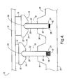
- Fig. 4 illustrates a side plan view of a thermal transfer assembly 10 according to yet another embodiment of the invention.
- the thermal transfer assembly 10 is shown incorporating two integrated circuits 14.
- Each of the integrated circuits 14 are at different elevations.
- the biasing device 21 proximate the condenser end 30 of each thermal pin 32 yields a different compression to therefore equalize the pressure on each of the corresponding integrated circuits 14. This feature highlights the ability of the invention to adjust for variant elevation integrated circuits 14.
- the thermal transfer device 18 is a thermal pipe 34.
- the thermal pipe 34 includes side walls that form a longitudinal center opening that extends along the length of the pipe 34.
- the condenser end 30 of the thermal pipe 34 forms an elbow 50 that rests on a portion of thermal dissipating device 20.
- the thermal dissipating device 20 includes a receiving portion 52. In this manner, the receiving portion 52 forms a receptacle for the elbow 52.
- the biasing device 21 is integrated or disposed in the receiving portion 52.
- the elbow 50 of the thermal pipe 34 contacts the biasing device 21 so that sufficient force is added between the evaporator end 28 of the thermal pipe 34 and the aperture 26 of the thermal conductor 16.
- the biasing device 21 is a flexible elastomeric material 54.
- multiple thermal pipes 34 such as the one herein described may also be incorporated into Fig. 5.
- the inclusion of the elastomeric material 54 provides that multiple integrated circuit elevations may be included and will not be adversely affected by the elevation as the invention. Similarly, this substantially eliminates the traditional concern involved with conventional overstressing
- the thermal junction includes a substrate and an integrated circuit connected thereto.
- Step S6.1 illustrates that a thermal conductor is attached to the integrated circuit, wherein the thermal conductor is larger than the integrated circuit in at least one dimension.
- Step S6.2 illustrates that an end of a thermal transfer device is inserted into an aperture of the thermal conductor such that a portion of the end is in thermal communication with the integrated circuit.
- a biasing device is disposed between the thermal transfer device and a thermal dissipating device connected thereto such that a small amount of force is applied between the thermal transfer device and the thermal conductor in step S6.3.
- the force from the at least one biasing device urges the thermal conductor to become substantially planar with the integrated circuit such that the surfaces thereof are substantially aligned in step S6.4 while not overstressing the integrated circuit 14.
Landscapes
- Cooling Or The Like Of Semiconductors Or Solid State Devices (AREA)
- Cooling Or The Like Of Electrical Apparatus (AREA)
- Connecting Device With Holders (AREA)
Applications Claiming Priority (1)
| Application Number | Priority Date | Filing Date | Title |
|---|---|---|---|
| US11/093,537 US20060221571A1 (en) | 2005-03-30 | 2005-03-30 | Thermal conductor and use thereof |
Publications (2)
| Publication Number | Publication Date |
|---|---|
| EP1708262A2 true EP1708262A2 (de) | 2006-10-04 |
| EP1708262A3 EP1708262A3 (de) | 2009-09-16 |
Family
ID=36619476
Family Applications (1)
| Application Number | Title | Priority Date | Filing Date |
|---|---|---|---|
| EP06075616A Withdrawn EP1708262A3 (de) | 2005-03-30 | 2006-03-16 | Thermischer Leiter und dessen Verwendung |
Country Status (2)
| Country | Link |
|---|---|
| US (1) | US20060221571A1 (de) |
| EP (1) | EP1708262A3 (de) |
Family Cites Families (18)
| Publication number | Priority date | Publication date | Assignee | Title |
|---|---|---|---|---|
| US4153107A (en) * | 1977-06-30 | 1979-05-08 | International Business Machines Corporation | Temperature equalizing element for a conduction cooling module |
| US4246597A (en) * | 1979-06-29 | 1981-01-20 | International Business Machines Corporation | Air cooled multi-chip module having a heat conductive piston spring loaded against the chips |
| US4235283A (en) * | 1979-12-17 | 1980-11-25 | International Business Machines Corporation | Multi-stud thermal conduction module |
| US4462462A (en) * | 1981-11-17 | 1984-07-31 | International Business Machines Corporation | Thermal conduction piston for semiconductor packages |
| US4639829A (en) * | 1984-06-29 | 1987-01-27 | International Business Machines Corporation | Thermal conduction disc-chip cooling enhancement means |
| JPH063831B2 (ja) * | 1987-04-08 | 1994-01-12 | 株式会社日立製作所 | 冷却装置及びそれを用いた半導体装置 |
| US4765400A (en) * | 1987-04-14 | 1988-08-23 | International Business Machines Corp. | Circuit module with pins conducting heat from floating plate contacting heat producing device |
| US5005638A (en) * | 1988-10-31 | 1991-04-09 | International Business Machines Corporation | Thermal conduction module with barrel shaped piston for improved heat transfer |
| JPH04139753A (ja) * | 1990-09-29 | 1992-05-13 | Toshiba Corp | 伝熱キャップ |
| US5323818A (en) * | 1993-04-28 | 1994-06-28 | International Business Machines Corporation | Apparatus and process for dispensing thermal paste into a thermal conduction module cold plate |
| JPH1070219A (ja) * | 1996-08-27 | 1998-03-10 | Fujitsu Ltd | 実装モジュールの冷却装置 |
| JP3241639B2 (ja) * | 1997-06-30 | 2001-12-25 | 日本電気株式会社 | マルチチップモジュールの冷却構造およびその製造方法 |
| US6570247B1 (en) * | 1997-12-30 | 2003-05-27 | Intel Corporation | Integrated circuit device having an embedded heat slug |
| US6214647B1 (en) * | 1998-09-23 | 2001-04-10 | International Business Machines Corporation | Method for bonding heatsink to multiple-height chip |
| US20050039880A1 (en) * | 2001-12-26 | 2005-02-24 | Scott Alexander Robin Walter | Computer cooling apparatus |
| US6867976B2 (en) * | 2002-02-12 | 2005-03-15 | Hewlett-Packard Development Company, L.P. | Pin retention for thermal transfer interfaces, and associated methods |
| US20040226688A1 (en) * | 2003-04-30 | 2004-11-18 | Arthur Fong | Application specific apparatus for dissipating heat from multiple electronic components |
| US20060060328A1 (en) * | 2004-09-21 | 2006-03-23 | Ingo Ewes | Heat-transfer devices |
-
2005
- 2005-03-30 US US11/093,537 patent/US20060221571A1/en not_active Abandoned
-
2006
- 2006-03-16 EP EP06075616A patent/EP1708262A3/de not_active Withdrawn
Also Published As
| Publication number | Publication date |
|---|---|
| EP1708262A3 (de) | 2009-09-16 |
| US20060221571A1 (en) | 2006-10-05 |
Similar Documents
| Publication | Publication Date | Title |
|---|---|---|
| US5944093A (en) | Pickup chuck with an integral heat pipe | |
| US7435102B2 (en) | Interconnecting electrical devices | |
| CN1909424B (zh) | 具有有源热量传输的光转发器 | |
| US6970358B2 (en) | Stack up assembly | |
| US7365923B2 (en) | Heat sink tab for optical sub-assembly | |
| US9804223B2 (en) | Systems and methods for conforming test tooling to integrated circuit device with heater socket | |
| US20100132925A1 (en) | Partable Thermal Heat Pipe | |
| US6565367B2 (en) | Zero insertion force compliant pin contact and assembly | |
| WO2006049737A2 (en) | A new thermally enhanced molded package for semiconductors | |
| US20070069369A1 (en) | Heat dissipation device and method for making the same | |
| US6867976B2 (en) | Pin retention for thermal transfer interfaces, and associated methods | |
| US6498551B1 (en) | Millimeter wave module (MMW) for microwave monolithic integrated circuit (MMIC) | |
| US20200245446A1 (en) | Pcb assembly and method of manufacturing a pcb assembly | |
| US6256202B1 (en) | Integrated circuit intercoupling component with heat sink | |
| US6164993A (en) | Zero insertion force sockets using negative thermal expansion materials | |
| US7270176B2 (en) | System and apparatus for fixing a substrate with a heat transferring device | |
| EP1708262A2 (de) | Thermischer Leiter und dessen Verwendung | |
| US8584743B2 (en) | Solid type heat dissipation device | |
| JP2012077988A (ja) | 熱中継機構及び放熱フィン | |
| TWI292089B (en) | Dissipation module | |
| US20150022226A1 (en) | Systems and methods for conforming test tooling to integrated circuit device profiles with coaxial socket | |
| US20140352925A1 (en) | Heat pipe structure | |
| US20050225945A1 (en) | Universal mountable heat sink with integral spring clip | |
| US20070010111A1 (en) | Temperature dependent semiconductor module connectors | |
| JP2003152368A (ja) | 電子機器 |
Legal Events
| Date | Code | Title | Description |
|---|---|---|---|
| PUAI | Public reference made under article 153(3) epc to a published international application that has entered the european phase |
Free format text: ORIGINAL CODE: 0009012 |
|
| AK | Designated contracting states |
Kind code of ref document: A2 Designated state(s): AT BE BG CH CY CZ DE DK EE ES FI FR GB GR HU IE IS IT LI LT LU LV MC NL PL PT RO SE SI SK TR |
|
| AX | Request for extension of the european patent |
Extension state: AL BA HR MK YU |
|
| PUAL | Search report despatched |
Free format text: ORIGINAL CODE: 0009013 |
|
| AK | Designated contracting states |
Kind code of ref document: A3 Designated state(s): AT BE BG CH CY CZ DE DK EE ES FI FR GB GR HU IE IS IT LI LT LU LV MC NL PL PT RO SE SI SK TR |
|
| AX | Request for extension of the european patent |
Extension state: AL BA HR MK YU |
|
| AKX | Designation fees paid | ||
| REG | Reference to a national code |
Ref country code: DE Ref legal event code: 8566 |
|
| STAA | Information on the status of an ep patent application or granted ep patent |
Free format text: STATUS: THE APPLICATION IS DEEMED TO BE WITHDRAWN |
|
| 18D | Application deemed to be withdrawn |
Effective date: 20100317 |