EP1703396A2 - Error detection & correction - Google Patents
Error detection & correction Download PDFInfo
- Publication number
- EP1703396A2 EP1703396A2 EP05253847A EP05253847A EP1703396A2 EP 1703396 A2 EP1703396 A2 EP 1703396A2 EP 05253847 A EP05253847 A EP 05253847A EP 05253847 A EP05253847 A EP 05253847A EP 1703396 A2 EP1703396 A2 EP 1703396A2
- Authority
- EP
- European Patent Office
- Prior art keywords
- data
- data processing
- information exchange
- error
- exchanging
- Prior art date
- Legal status (The legal status is an assumption and is not a legal conclusion. Google has not performed a legal analysis and makes no representation as to the accuracy of the status listed.)
- Granted
Links
Images






Classifications
-
- G—PHYSICS
- G06—COMPUTING OR CALCULATING; COUNTING
- G06F—ELECTRIC DIGITAL DATA PROCESSING
- G06F11/00—Error detection; Error correction; Monitoring
-
- G—PHYSICS
- G06—COMPUTING OR CALCULATING; COUNTING
- G06F—ELECTRIC DIGITAL DATA PROCESSING
- G06F11/00—Error detection; Error correction; Monitoring
- G06F11/07—Responding to the occurrence of a fault, e.g. fault tolerance
- G06F11/08—Error detection or correction by redundancy in data representation, e.g. by using checking codes
- G06F11/10—Adding special bits or symbols to the coded information, e.g. parity check, casting out 9's or 11's
- G06F11/1008—Adding special bits or symbols to the coded information, e.g. parity check, casting out 9's or 11's in individual solid state devices
- G06F11/1044—Adding special bits or symbols to the coded information, e.g. parity check, casting out 9's or 11's in individual solid state devices with specific ECC/EDC distribution
-
- G—PHYSICS
- G06—COMPUTING OR CALCULATING; COUNTING
- G06F—ELECTRIC DIGITAL DATA PROCESSING
- G06F11/00—Error detection; Error correction; Monitoring
- G06F11/07—Responding to the occurrence of a fault, e.g. fault tolerance
- G06F11/14—Error detection or correction of the data by redundancy in operations
Definitions
- the present invention relates to a control method for error detection & correction apparatus, an error detection & correction apparatus, an information processing system, a control program for error detection & correction apparatus, a data processing apparatus, and in particular a technique effectively applicable to a detection and correction of data error, et cetera, by using an error correcting code (ECC) in a data transmission or accumulation.
- ECC error correcting code
- known is a method of using an ECC for detecting and correcting a data error which occurs in a bus as information transmission path or memory storing information.
- error check unit In the case of letting one ECC processing apparatus process a unit of error check ("error check unit” hereinafter unlessotherwise noted)in an ECC application, it is necessary to increase the number of pins in the ECC processing apparatus according to a data size of the error check unit, or transmit data by folding itself.
- Acountermeasure is conceivable to have a plurality of ECC processing apparatuses share the error check unit, in which a method is adopted such that each ECC processing apparatus sharing the processing of the error check unit performs a partial error check and a processing apparatus in upper echelon (e.g., a controller or CPU in upper echelon) achieves a final error check and correction of the error check unit.
- a method is known to exchange a partial syndrome between a plurality of ECC processing apparatuses sharing an error check unit and generate a true syndrome of the error check unit, as disclosed by the patent documents 1 or 2 listed below.
- an error check & correction circuit comprising means for outputting a partial syndrome to the outside by generating it based on a part of a codeword being inputted from the outside, means for generating a syndrome of a codeword based on the partial syndrome inputted from the outside and partial syndrome generated in the inside, and means for correcting a partial error of a codeword by decoding the generated syndrome.
- the patent document 2 has disclosed a technique to enable a plurality of ECC circuits with the exact same configuration to share-process a multi-bit data by making the ECC circuits sharing each of a plurality of blocks adaptable to either of an upper bit block or lower bit block by an external control signal only, in the case of generating an ECC for each of a plurality of blocks which are obtained by dividing a multi-bit data into plural parts.
- each ECC processing apparatus sharing the error check unit will no longer be able to handle a high level data processing (e. g., a data processing onlypossible following an error check such as a partial merge of data) .
- a high level data processing e. g., a data processing onlypossible following an error check such as a partial merge of data
- a purpose of the present invention is to enable each processing apparatus to perform a high level data processing such as requiring a merge processing of data in an error detection & correction technique for processing data by the unit of ECC error check in a plurality of partaking processing apparatuses.
- Another purpose of the present invention is to enable each processing apparatus to perform a diverse error detection & correction processing corresponding to a category of detected error, et cetera, in an error detection & correction technique for processing data by the unit of ECC error check in a plurality of partaking processing apparatuses.
- Yet another purpose of the present invention is to accomplish an error detection & correction capability equivalent to the case in which one data processing apparatus processes data by the unit of ECC error check.
- a first aspect of the present invention is to provide a control method for an error detection & correction apparatus, comprising a plurality of data processing apparatuses which reside in a data communication path and partake in exchanging data by the unit of error correcting code, and a plurality of information exchange paths which are installed between the plurality of data processing apparatuses; and generating a true syndrome by exchanging a partial syndrome relating to a part of the data partaken by each of the data processing apparatuses by way of the information exchange paths, comprising the step of exchanging renewal information relating to a part of the data partaken by each of the data processing apparatuses with the other data processing apparatus by way of the information exchange path.
- a second aspect of the present invention is to provide an error detection & correction apparatus, comprising a plurality of data processing apparatuses which reside in a data communication path and partake in exchanging data by the unit of error correcting code and a plurality of information exchange paths which are installed between the plurality of data processing apparatuses; and generating a true syndrome by exchanging a partial syndrome relating to a part of the data partaken by each of the data processing apparatuses by way of the information exchange paths, comprising: an information exchange unit for exchanging renewal information relating to a part of the data partaken by each of the data processing apparatuses with the other data processing apparatus by way of the information exchange path.
- a third aspect of the present invention is to provide an information processing system, including a storage apparatus, an access apparatus for accessing the storage apparatus, a data transmission path for connecting the storage apparatus with the access apparatus and an error detection & correction apparatus residing in the data transmission path, wherein the error detection & correction apparatus comprises a plurality of data processing apparatuses partaking in exchanging data by the unit of error correcting code in data transmission paths, information exchange paths installed between a plurality of the data processing apparatuses, and an information exchange unit for exchanging a partial syndrome relating to a part of the data partaken by each of the data processing apparatuses and renewal information relating to a part of the data partaken by each of the data processing apparatus with a plurality of the data processing apparatuses by way of the information exchange paths.
- a fourth aspect of the present invention is to provide a signal for carrying control program, for an error detection & correction apparatus comprising a plurality of data processing apparatuses which reside in a data communication path and partake in exchanging data by the unit of error correcting code, and a plurality of information exchange paths which are installed between the plurality of data processing apparatuses, wherein the signal for carrying control program makes each of the data processing apparatuses carry out the process of exchanging a partial syndrome relating to a part of the data partaken by each of the data processing apparatuses and renewal information relating to a part of the data partaken by each of the data processing apparatus with a plurality of the data processing apparatuses by way of the information exchange paths.
- a fifth aspect of the present invention is to provide a data processing apparatus, being included in an error detection & correction apparatus residing in a data communication path and partaking in exchanging data by the unit of error correcting code, comprising an information exchange unit for exchanging a partial syndrome relating to a part of the data partaken by the own apparatus and renewal information relating to a part of the data partaken by own apparatus with other data processing apparatus.
- each of data processing apparatuses is enabled for a high level data processing such as a partial data merge by exchanging error correction information between a plurality of data processing apparatuses instead of being limited by a partial syndrome, in an error detection & correction technique for processing data by the unit of ECC error check ("ECC error check unit” hereinafter unless otherwise noted) in a plurality of partaking processing apparatuses.
- ECC error check unit the unit of ECC error check
- a high level data processing such as a read modify write (i.e., a partial data merge) is enabled even if data by the ECC error check unit is processed across a plurality of data processing apparatuses, each of which is configured to deal with data protected by the ECC, such as a memory controller.
- a read modify write i.e., a partial data merge
- a diverse error detection and correction processing in response to a detected error are enabled by exchanging error correction information other than partial syndromes between a plurality of data processing apparatuses. Furthermore, an error detection & correction capability equivalent to the case of a single data processing apparatus dealing with data by an error check unit can be achieved.
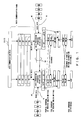
- Fig. 1 is a conceptual diagram showing an example operation of error detection & correction apparatus according to an embodiment of the present invention
- Fig. 2 is a conceptual diagram showing a modified operation of error detection & correction apparatus according to an embodiment of the present invention.
- Fig. 3 is a block diagram showing an example comprisal of data processing apparatus constituting a memory access control apparatus as an example of error detection & correction apparatus according to an embodiment of the present invention
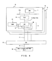
- Fig. 4 is a conceptual diagram showing an example comprisal of information processing system according to an embodiment of the present invention.
- the information processing system according to the present embodiment comprises a plurality of information processing apparatuses 10, a bus switch 20 (i.e., GDX) and one or a plurality of input & output equipments 30 (i . e . , FLI) .
- a bus switch 20 i.e., GDX
- input & output equipments 30 i . e . , FLI
- the bus switch 20 switches connections of information transmission paths between these information processing apparatuses 10 and input & output equipment 30.
- the each of information processing apparatuses 10 includes a CPU 11, a system bus 11a, an input & output control apparatus 12 (i.e., FLN), a memory apparatus 13 (i.e., DIMM), a memory access control apparatus 14 (i.e., error detection & correction apparatus) (LDX), an upper side bus 15, a memory bus 16 and a lower side bus 17.
- a CPU 11 a system bus 11a
- an input & output control apparatus 12 i.e., FLN
- a memory apparatus 13 i.e., DIMM
- a memory access control apparatus 14 i.e., error detection & correction apparatus
- the CPU 11 executes an information processing by accessing to a program and data stored in the memory apparatus 13.
- the input & output control apparatus 12 controls information exchanges between the CPU 11 and the memory apparatus 13, other information processing apparatuses 10 and input & output equipment 30.
- the memory apparatus 13 stores a program and data executed by the CPU 11.
- the memory access control apparatus 14 functions as an error detection & correction apparatus in the case of the present embodiment. That is, the memory access control apparatus 14 performs an error detection & correction by using an ECC for data read / written, out of / in, the memory apparatus 13 by way of the memory bus 16, upper side bus 15 and lower side bus 17.
- Each of the memory access control apparatus 14 is constituted by a plurality of data processing apparatuses 40 (LDX), each of which comprises as exemplified by Fig. 3.
- LDX data processing apparatuses 40
- each data processing apparatus 40 comprises a memory access control logic 41, a write buffer 42 (WRQ), a read buffer 43 (RDQ) and an information exchange buffer 44 (ECC).
- WRQ write buffer 42
- RDQ read buffer 43
- ECC information exchange buffer 44
- a plurality of the data processing apparatuses 40 are interconnected by an information exchange bus 50 (i.e., information exchange path).
- the write buffer 42 temporarily stores write data to be written in the memory apparatus 13 from the CPU 11, other information processing apparatus 10, input & output equipment 30, et cetera.
- the read buffer 43 temporarily stores read data which is read out of the memory apparatus 13.
- the memory access control logic 41 comprises a control logic (i.e., control program) in the form of software, firmware or hardware for accomplishing the functions as described below.
- control logic i.e., control program
- the memory access control logic 41 comprises the function of performing an ECC processing for a read or write data in a data width of the upper side bus 15 and lower side bus 17 by sharing with other partaking data processing apparatus 40 by exchanging a series of information therewith by way of the information exchange bus 50.
- the memory access control logic 41 comprises the function of enabling a conversion and error check & correction of a check bit also at the time of partially renewing data by the ECC error check unit for the upper side bus 15, memory bus 16 and lower side bus 17.
- the memory access control logic 41 comprises the function of selecting an operation for using, or not using, the information exchange bus 50 for data by the unit of ECC error check in response to a pattern of partial renewal information.
- the memory access control logic 41 comprises the function of altering a check bit (i.e., renewing) which regards all the data partaken by the other data processing apparatuses 40 as zero (0) for the data after being partially renewed, not for the partial renewal information at the time of error correction, and of exchanging with the other data processing apparatus 40 by way of the information exchange bus 50.
- a check bit i.e., renewing
- the memory access control logic 41 comprises the function of exchanging detected information of a specific error pattern which has been detected within its own apparatus with the other data processing apparatus 40 by way of the information exchange bus 50, and changing an error correction operation.
- the memory access control logic 41 comprises the function of preventing an erroneous correction due to a use of a wrong partial syndrome through the steps of adding a synchronism confirmation signal to a partial syndrome, and an ECC protection to the information exchange bus 50 per se as well; exchanging with the other data processing apparatus 40 by way of the aforementioned information exchange bus 50; and detecting an erroneous usage timing of the partial syndrome in own apparatus and the other data processing apparatuses 40.
- the memory access control logic 41 comprises the function of controlling a data length variably of a partial syndrome being exchanged with other data processing apparatus 40 by way of the information exchange bus 50.
- the memory access control logic 41 comprises the function of not only sending corrected data by exchanging a partial syndrome by way of the information exchange bus 50 out to the input & output control apparatus 12, et cetera, but also sending out pre-correction data in advance followed by notifying of a detected error afterwards.
- An example practice is to divide a 128-byte data into four of LDX / DIMM and make the best use of the upper side bus 15 and/or lower side bus 17 between FLN - LDX and/or FLN - GDX in order to minimize a transmission latency of a 128-byte cache line in the CPU 11. Consequently, as a 16-byte ECC straddles two LDXes, do not basically perform an error check and instead let the LDX transmit the data, S4EC - D4ED (Single 4-bit block Error Correction / Double 4-bit block Error Detection) -code, as is, to the devices such as FLN and FLI.
- S4EC - D4ED Single 4-bit block Error Correction / Double 4-bit block Error Detection
- Fig. 5 shows a bus as a subject of protection by an ECC (16-byte S4EC - D4ED) by a 32 SMP (symmetrical multi processor) basic comprisal.
- the FLN i.e., input & output control apparatus 12
- FLI i.e., input & output equipment 30
- the LDX also performs the check & correction in order to complete an identification of error spot, a later described patrol in the DIMM (i.e., memory apparatus 13) and a data moving at the time of partial write such as a read modify write, all within the LDX.
- the information exchange bus 50 comprises two kinds of buses, i.e., bus #0 and bus #1, whose data transmission directions are mutually the opposite.
- the next description is about an error control by the memory access control logic 41 performed by each of the data processing apparatuses 40 (i.e., LDX) constituting the memory access control apparatus 14.
- the memory access control apparatus 14 comprising a plurality of LDXes performs the operations of a memory read, memory write, partial write (i.e., read modify write) and patrol (i.e., periodical operation monitor processing), all for accessing to the memory apparatus 13.
- an exchange of syndrome is performed by using the information exchange bus 50 which will also be used for a data transmission path at the time of a degenerate operation.
- a transmission protocol for the information exchange bus 50 will be described later.
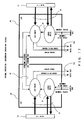
- the plurality of data processing apparatuses 40 i.e., LDXes #0 / #1
- a data width of the ECC error check unit e.g. 16 bytes
- transmit a partial syndrome detected within own apparatus to the other partaking apparatus by way of the information exchange bus 50. That is, to generate a syndrome to send out to the other apparatus by setting zero (0) as the value for the other 8 bytes of data partaken by the other LDX. If there is no error in the data, the values of mutually sent syndromes are the same.
- the memory access control logic 41 comprised by the LDX reports the error to an FLN in an upper echelon through a reply bus 15b.
- An error is classified into three types (i.e., SBE: singleblockerror (correctable), DBE: double block error (uncorrectable) and detection of poisoned data) for each of the four memory operations (i.e., memory read, memory write, partial write and patrol) in the error report.
- SBE singleblockerror
- DBE double block error
- detection of poisoned data i.e., memory read, memory write, partial write and patrol
- LDXes #0 and #1, or LDXes #2 and #3, in the example shown by Fig. 5 straddled by an ECC check unit report the same content, except for a memory write at a degenerate operation, et cetera, in which only one LDX in a team may report.
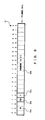
- Fig. 7A is a conceptual diagram showing an example comprisal of the information exchange bus 50 according to the present embodiment.
- the information exchange bus 50 comprises the bus #0 and bus #1, with each thereof comprising respective signals by the bit widths (i.e., the numbers of pins) as exemplified by Fig. 7B.
- the transmitted data is protected by the 21-bit data ECC (i.e., SEC - DED) in either the bus #0 or bus #1 constituting the information exchange bus 50.
- ECC 21-bit data ECC
- Fig. 8 describes an example setup of identifier information about information packet exchanged between LDXes by way of the information exchange bus 50.
- Figs. 9, 10, 11 and 12 are conceptual diagrams exemplifying respective formats of various packets.
- Fig. 9 shows an example configuration of syndrome exchange packet 51 for exchanging a syndrome.
- the syndrome exchange packet 51 comprises an ID part 51a, a reserve part 51b, error identifier information 51c and a syndrome value 51d.
- the ID part 51a is set with "100" corresponding to a "syndrome exchange” shown by Fig. 8.
- the error identifier information 51c is set with an information bit for identifying a poisoned data or otherwise.
- a configuration may be such that, if the error identifier information 51c is set, the syndrome value 51d stores information for indicating an error category instead of a syndrome value so as to exchange between the corresponding LDXes and switch the error correction operation in the respective LDXes.
- Fig. 10 shows an example configuration of renewal information exchange packet 52 for exchanging renewal information.
- the renewal information exchange packet 52 comprises an ID part 52a, a reserve part 52b, an operation change flag 52c and renewal information 52d.
- the ID part 52a is set with "101" corresponding to a "renewal information exchange” shown by Fig. 8.
- the renewal information 52d stores a post-correction data obtained by the LDX which has transmitted the aforementioned renewal information exchange packet 52.
- the operation change flag 52c is used for changing an operation if a specific error pattern is detected as a result of the LDXes notifying each other of detecting the aforementioned specific error pattern.
- Fig. 11 shows an example configuration of synchronism check packet 53 for a synchronism check.
- the synchronism check packet 53 comprises an ID part 53a and synchronism identifier information 53b.
- the ID part 53a is set with "001" corresponding to a "synchronism check" shown by Fig. 8.
- the synchronism identifier information 53b is set with a Sync-ID for controlling a synchronism between the LDXes.
- a synchronism check is for controlling a synchronism between the LDXes #0 and #1, and between the LDXes #2 and #3, mutually partaking in the ECC data unit, not checking the synchronism among all the LDXes.
- Fig. 12 shows an example configuration of data packet 54 at the time of a degenerate operation ("at-degenerate operation data packet 54" hereinafter) .
- the at-degenerate operation data packet 54 comprises an ID part 54a and transmission data 54b.
- the ID part 54a is set with "111" corresponding to a "degenerate operation data transmission” shown by Fig. 8.
- the transmission data 54b stores transmission data at a degenerate operation.
- Fig. 13 describes a list of error check control by each LDX, showing the error check operation in the operations of a read, write, p-write (i.e., partial write) and patrol.
- Fig. 14 shows a read operation by the memory apparatus 13 (i.e., DIMM) at the normal operation.
- the memory access control logic 41 participate in executing an ECC check for readout data by transmitting the read data out of the memory apparatus 13 to the input & output control apparatus 12 and exchanging the partial syndrome values by way of the information exchange bus 50.
- the transmission of the data to the input & output control apparatus 12 is put in a higher priority and an error will be reported thereto later by using the reply bus 15b if the error is detected in the readout data.
- a data read from the memory apparatus 13 to the input & output equipment 30 will likewise be done.
- the memory access control logic 41 performs a Scrub Write demand to the input & output control apparatus 12 by way of the replybus 15b and executes a Scrub Write, which repairs stored data within the memory apparatus 13, for a storage zone of an address instructed by the input & output control apparatus 12 by way of the address bus 15a.
- Fig. 15 shows an operation of the LDX in a write operation for the memory apparatus 13.
- a plurality of LDXes partake in executing an ECC check and correction for the write data coming in from the input & output control apparatus 12 by way of the upper side bus 15, and, if an error is detected, the memory access control logic 41 comprised in the inside of each LDX corrects the error to write in the memory apparatus 13 and also reports the error to the input & output control apparatus 12 by way of the reply bus 15b.
- a data write processing for the data from the input & output equipment 30 to the memory apparatus 13 will likewise be done.
- Fig. 16 shows an operation of the LDX in a partial write (i.e., read modify write) for the memory apparatus 13.
- each LDX Having received a write data from an FLN or GDX, each LDX performs an ECC check and correction by mutually exchanging syndromes, and reports an error to the FLN by way of the reply bus 15b if the error is detected.
- each LDX also performs an ECC check and correction by mutually exchanging syndromes, and report an error to the FLN by way of the reply bus 15b if the error is detected.
- each LDX mutually exchanges correction results relating to the write and read data as the renewal information by way of the information exchange bus 50.
- the LDX merges the write data processed through the ECC check & correction and the read data out of the DIMM by including the ECC check bit to write in the DIMM. If a DBE (double block error) or a Poisoned Data is detected as a result of the ECC check, the Poisoned Data will be written in the DIMM.
- the present embodiment lets the two LDXes partaking in the ECC check & correction exchange with each other the renewal information for the own apparatuses reflected by the correction result of the read data and that of the write data, in addition to two syndromes relating to the read and write data by way of the information exchange bus 50 .
- the exchange of the renewal information uses the above described renewal information exchange packet 52.
- Fig. 17 shows an operation of the LDX in the patrol. After reading data out of the DIMM, each LDX performs an ECC check by exchanging syndromes by way of the information exchange bus 50 and reports an error to the FLN by way of the reply bus 15b if the error is detected.
- the LDX demands a Scrub Write to the FLN to correct the error in the DIMM.
- the two data processing apparatuses 40 partaking in an ECC check simultaneously receive a write data through the data communication path (i.e., upper side bus 15 or lower side bus 17).
- the LDX (#0) and LDX (#1) send partial syndromes SD-AO and SD-BO, respectively, to each other, generate a true syndrome SD-ABO and perform an error correction. Likewise they further perform an error correction operation.
- the sequence of write and read operations is not important.
- the LDXes #0 and #1 transmit renewal information (i.e., a changed part by the error correction operation) to each other, merge the data and reconstruct a check bit.
- each LDX can change an operation at an ECC error detection when detecting a specific error pattern by using the above described operation change flag 52c of the renewal information exchange packet 52, which will be described in reference to Fig. 2.
- the description associated with Fig. 2 is about a pair of LDXes (#0) and (#1).
- Fig. 2 exemplifies the case of suppressing an error correction operation, if detecting a specific error pattern, by the LDXes exchanging the aforementioned specific error pattern with each other by way of the information exchange bus 50 with a use of the operation change flag 52c of the renewal information exchange packet 52 (Fig. 10).
- the renewal information 52d stores the specific error pattern causing the error.
- Such control operationperformedby the LDX is quite useful in an information processing system adopting the method of identifying an error occurrence point or controlling a program flow by the error marking, that is, by an apparatus which has detected the error, or embedded the error therein, exchanging data in a specific data pattern and constituting an ECC error.
- the practice is to enable an error check by adding a synchronism signal to a syndrome data at the discretionary timing by using the synchronism check packet 53 in order to prevent a correct data from an erroneous correction as a result of the LDXes exchanging erroneous syndromes with each other.
- the present embodiment enables each of a plurality of data processing apparatuses 40 constituting the memory access control apparatus 14 to perform high level processing functions therein, such as a readmodifywrite (i.e., partial write) accompanying a data merge in order to perform an error check by exchanging renewal information, i.e., post-correction data, in addition to exchanging the syndromes.
- a readmodifywrite i.e., partial write
- renewal information i.e., post-correction data
- the data processing apparatuses 40 exchange syndromes and the minimum amount of necessary information only, thereby minimizing a bus width between the data processing apparatuses 40.
- an ECC check with an equivalent error detection & correction capability comparable to the case of processing by a single data processing apparatus can be accomplished in an apparatus dealing with data protected by an ECC such as the memory access control apparatus 14 comprising a plurality of data processing apparatuses 40 for example.
- an equivalent error detection & correction capability comparable to the case of processing by a single data processing apparatus can be accomplished for a high level data processing such as a read modify write (i.e., partial data merge).
- a read modify write i.e., partial data merge
- each processing apparatus is enabled for a high level data processing so as to require a data merge in an error detection & correction technique for a plurality of the processing apparatuses partaking in processing data by the ECC error check unit.
- each processing apparatus is enabled for various kinds of error detection & correction processing in response to the detected error categories in an error detection & correction technique for a plurality of the processing apparatuses partaking in processing data by the ECC error check unit.
- an equivalent error detection & correction capability comparable to the case of processing data by the unit of ECC error check by a single data processing apparatus can be accomplished in an error detection & correction technique for a plurality of the processing apparatuses partaking in processing data by the ECC error check unit.
Landscapes
- Engineering & Computer Science (AREA)
- Theoretical Computer Science (AREA)
- Quality & Reliability (AREA)
- Physics & Mathematics (AREA)
- General Engineering & Computer Science (AREA)
- General Physics & Mathematics (AREA)
- Detection And Correction Of Errors (AREA)
- Techniques For Improving Reliability Of Storages (AREA)
- Error Detection And Correction (AREA)
- Detection And Prevention Of Errors In Transmission (AREA)
Abstract
Description
- The present invention relates to a control method for error detection & correction apparatus, an error detection & correction apparatus, an information processing system, a control program for error detection & correction apparatus, a data processing apparatus, and in particular a technique effectively applicable to a detection and correction of data error, et cetera, by using an error correcting code (ECC) in a data transmission or accumulation.
- In an information processing system, known is a method of using an ECC for detecting and correcting a data error which occurs in a bus as information transmission path or memory storing information.
- In the case of letting one ECC processing apparatus process a unit of error check ("error check unit" hereinafter unlessotherwise noted)in an ECC application, it is necessary to increase the number of pins in the ECC processing apparatus according to a data size of the error check unit, or transmit data by folding itself.
- However, an increase of the number of pins in the ECC processing apparatus in proportion to a data size ushers in an increased production cost thereof. And a transmission of folded data causes a one-bit failure in a pin or data transmission path to multiply to a plural-bit failure, hence bringing about a reliability problem of error recovery becoming impossible.
- Acountermeasure is conceivable to have a plurality of ECC processing apparatuses share the error check unit, in which a method is adopted such that each ECC processing apparatus sharing the processing of the error check unit performs a partial error check and a processing apparatus in upper echelon (e.g., a controller or CPU in upper echelon) achieves a final error check and correction of the error check unit. Alternatively, a method is known to exchange a partial syndrome between a plurality of ECC processing apparatuses sharing an error check unit and generate a true syndrome of the error check unit, as disclosed by the
patent documents - In specifics, the technique brought forth by the
patent document 1 has disclosed an error check & correction circuit comprising means for outputting a partial syndrome to the outside by generating it based on a part of a codeword being inputted from the outside, means for generating a syndrome of a codeword based on the partial syndrome inputted from the outside and partial syndrome generated in the inside, and means for correcting a partial error of a codeword by decoding the generated syndrome. - And the
patent document 2 has disclosed a technique to enable a plurality of ECC circuits with the exact same configuration to share-process a multi-bit data by making the ECC circuits sharing each of a plurality of blocks adaptable to either of an upper bit block or lower bit block by an external control signal only, in the case of generating an ECC for each of a plurality of blocks which are obtained by dividing a multi-bit data into plural parts. - If a processing apparatus in a higher echelon is to perform a data processing, however, each ECC processing apparatus sharing the error check unit will no longer be able to handle a high level data processing (e. g., a data processing onlypossible following an error check such as a partial merge of data) . Likewise, there has been a problem of a simple partial syndrome exchange being unable to make it possible to perform a high level data processing as noted above.
- [Patent document 1]
Japanese patent laid-open application publication No. 4- 023048 - [Patent document 2]
Japanese patent laid-open application publication No. 11- 232129 - A purpose of the present invention is to enable each processing apparatus to perform a high level data processing such as requiring a merge processing of data in an error detection & correction technique for processing data by the unit of ECC error check in a plurality of partaking processing apparatuses.
- Another purpose of the present invention is to enable each processing apparatus to perform a diverse error detection & correction processing corresponding to a category of detected error, et cetera, in an error detection & correction technique for processing data by the unit of ECC error check in a plurality of partaking processing apparatuses.
- Yet another purpose of the present invention is to accomplish an error detection & correction capability equivalent to the case in which one data processing apparatus processes data by the unit of ECC error check.
- A first aspect of the present invention is to provide a control method for an error detection & correction apparatus, comprising a plurality of data processing apparatuses which reside in a data communication path and partake in exchanging data by the unit of error correcting code, and a plurality of information exchange paths which are installed between the plurality of data processing apparatuses; and generating a true syndrome by exchanging a partial syndrome relating to a part of the data partaken by each of the data processing apparatuses by way of the information exchange paths, comprising the step of exchanging renewal information relating to a part of the data partaken by each of the data processing apparatuses with the other data processing apparatus by way of the information exchange path.
- A second aspect of the present invention is to provide an error detection & correction apparatus, comprising a plurality of data processing apparatuses which reside in a data communication path and partake in exchanging data by the unit of error correcting code and a plurality of information exchange paths which are installed between the plurality of data processing apparatuses; and generating a true syndrome by exchanging a partial syndrome relating to a part of the data partaken by each of the data processing apparatuses by way of the information exchange paths, comprising: an information exchange unit for exchanging renewal information relating to a part of the data partaken by each of the data processing apparatuses with the other data processing apparatus by way of the information exchange path.
- A third aspect of the present invention is to provide an information processing system, including a storage apparatus, an access apparatus for accessing the storage apparatus, a data transmission path for connecting the storage apparatus with the access apparatus and an error detection & correction apparatus residing in the data transmission path, wherein the error detection & correction apparatus comprises a plurality of data processing apparatuses partaking in exchanging data by the unit of error correcting code in data transmission paths, information exchange paths installed between a plurality of the data processing apparatuses, and an information exchange unit for exchanging a partial syndrome relating to a part of the data partaken by each of the data processing apparatuses and renewal information relating to a part of the data partaken by each of the data processing apparatus with a plurality of the data processing apparatuses by way of the information exchange paths.
- A fourth aspect of the present invention is to provide a signal for carrying control program, for an error detection & correction apparatus comprising a plurality of data processing apparatuses which reside in a data communication path and partake in exchanging data by the unit of error correcting code, and a plurality of information exchange paths which are installed between the plurality of data processing apparatuses, wherein the signal for carrying control program makes each of the data processing apparatuses carry out the process of exchanging a partial syndrome relating to a part of the data partaken by each of the data processing apparatuses and renewal information relating to a part of the data partaken by each of the data processing apparatus with a plurality of the data processing apparatuses by way of the information exchange paths.
- A fifth aspect of the present invention is to provide a data processing apparatus, being included in an error detection & correction apparatus residing in a data communication path and partaking in exchanging data by the unit of error correcting code, comprising an information exchange unit for exchanging a partial syndrome relating to a part of the data partaken by the own apparatus and renewal information relating to a part of the data partaken by own apparatus with other data processing apparatus.
- According to the above described present invention, each of data processing apparatuses is enabled for a high level data processing such as a partial data merge by exchanging error correction information between a plurality of data processing apparatuses instead of being limited by a partial syndrome, in an error detection & correction technique for processing data by the unit of ECC error check ("ECC error check unit" hereinafter unless otherwise noted) in a plurality of partaking processing apparatuses.
- For instance, a high level data processing, such as a read modify write (i.e., a partial data merge), is enabled even if data by the ECC error check unit is processed across a plurality of data processing apparatuses, each of which is configured to deal with data protected by the ECC, such as a memory controller.
- Also, a diverse error detection and correction processing in response to a detected error are enabled by exchanging error correction information other than partial syndromes between a plurality of data processing apparatuses. Furthermore, an error detection & correction capability equivalent to the case of a single data processing apparatus dealing with data by an error check unit can be achieved.
-
- Fig. 1 is a conceptual diagram showing an example operation of error detection & correction apparatus according to an embodiment of the present invention;
- Fig. 2 is a conceptual diagram showing a modified operation of error detection & correction apparatus according to an embodiment of the present invention;
- Fig. 3 is a block diagram showing an example comprisal of data processing apparatus constituting a memory access control apparatus as an example of error detection & correction apparatus according to an embodiment of the present invention;
- Fig. 4 is a conceptual diagram showing an example comprisal of information processing system according to an embodiment of the present invention;
- Fig. 5 is a conceptual diagram showing more specifically an example comprisal of information processing system according to an embodiment of the present invention;
- Fig. 6 is a conceptual diagram showing an operation of a plurality of data processing apparatuses constituting a memory access control apparatus according to an embodiment of the present invention;
- Fig. 7A is a conceptual diagram showing an example comprisal of information exchange bus between a plurality of data processing apparatuses constituting a memory access control apparatus according to an embodiment of the present invention;
- Fig. 7B describes an example of signal specification for an information exchange bus between a plurality of data processing apparatuses constituting a memory access control apparatus according to an embodiment of the present invention;
- Fig. 8 describes an example setup of identifier information about information packet exchanged between a plurality of data processing apparatuses constituting a memory access control apparatus according to an embodiment of the present invention;
- Fig. 9 is a conceptual diagram showing an example format for a syndrome exchange packet exchanged between a plurality of data processing apparatuses constituting a memory access control apparatus according to an embodiment of the present invention;
- Fig. 10 is a conceptual diagram showing an example format for a renewal information exchange packet exchanged between a plurality of data processing apparatuses constituting a memory access control apparatus according to an embodiment of the present invention;
- Fig. 11 is a conceptual diagram showing an example format for a synchronism check packet exchanged between a plurality of data processing apparatuses constituting a memory access control apparatus according to an embodiment of the present invention;
- Fig. 12 is a conceptual diagram showing an example format for an at-degenerate operation data packet exchanged between a plurality of data processing apparatuses constituting a memory access control apparatus according to an embodiment of the present invention;
- Fig. 13 describes a list of error check control by a plurality of data processing apparatuses constituting a memory access control apparatus according to an embodiment of the present invention;
- Fig. 14 is a conceptual diagram showing an example of memory read operation by a plurality of data processing apparatuses constituting a memory access control apparatus according to an embodiment of the present invention;
- Fig. 15 is a conceptual diagram showing an example of memory write operation by a plurality of data processing apparatuses constituting a memory access control apparatus according to an embodiment of the present invention;
- Fig. 16 is a conceptual diagram showing an example of partial write operation by a plurality of data processing apparatuses constituting a memory access control apparatus according to an embodiment of the present invention; and
- Fig. 17 is a conceptual diagram showing an example of patrol operation by a plurality of data processing apparatuses constituting a memory access control apparatus according to an embodiment of the present invention.
- The following is a detailed description of the preferred embodiment of the present invention while referring to the accompanying drawings.
- Fig. 1 is a conceptual diagram showing an example operation of error detection & correction apparatus according to an embodiment of the present invention; and Fig. 2 is a conceptual diagram showing a modified operation of error detection & correction apparatus according to an embodiment of the present invention.
- Fig. 3 is a block diagram showing an example comprisal of data processing apparatus constituting a memory access control apparatus as an example of error detection & correction apparatus according to an embodiment of the present invention; and Fig. 4 is a conceptual diagram showing an example comprisal of information processing system according to an embodiment of the present invention.
- First description is about a comprisal of information processing system according to the present embodiment while referring to Fig. 4. The information processing system according to the present embodiment comprises a plurality of
information processing apparatuses 10, a bus switch 20 (i.e., GDX) and one or a plurality of input & output equipments 30 (i . e . , FLI) . - The
bus switch 20 switches connections of information transmission paths between theseinformation processing apparatuses 10 and input &output equipment 30. - The each of
information processing apparatuses 10 includes aCPU 11, asystem bus 11a, an input & output control apparatus 12 (i.e., FLN), a memory apparatus 13 (i.e., DIMM), a memory access control apparatus 14 (i.e., error detection & correction apparatus) (LDX), anupper side bus 15, amemory bus 16 and alower side bus 17. - The
CPU 11 executes an information processing by accessing to a program and data stored in thememory apparatus 13. - The input &
output control apparatus 12 controls information exchanges between theCPU 11 and thememory apparatus 13, otherinformation processing apparatuses 10 and input &output equipment 30. - The
memory apparatus 13 stores a program and data executed by theCPU 11. The memoryaccess control apparatus 14 functions as an error detection & correction apparatus in the case of the present embodiment. That is, the memoryaccess control apparatus 14 performs an error detection & correction by using an ECC for data read / written, out of / in, thememory apparatus 13 by way of thememory bus 16,upper side bus 15 andlower side bus 17. - In other words, the data transferred through the
upper side bus 15,memory bus 16 andlower side bus 17 is protected by the ECC as described later. - Each of the memory
access control apparatus 14 is constituted by a plurality of data processing apparatuses 40 (LDX), each of which comprises as exemplified by Fig. 3. - Specifically, each
data processing apparatus 40 comprises a memoryaccess control logic 41, a write buffer 42 (WRQ), a read buffer 43 (RDQ) and an information exchange buffer 44 (ECC). A plurality of thedata processing apparatuses 40 are interconnected by an information exchange bus 50 (i.e., information exchange path). - The
write buffer 42 temporarily stores write data to be written in thememory apparatus 13 from theCPU 11, otherinformation processing apparatus 10, input &output equipment 30, et cetera. - The read
buffer 43 temporarily stores read data which is read out of thememory apparatus 13. - The memory
access control logic 41 comprises a control logic (i.e., control program) in the form of software, firmware or hardware for accomplishing the functions as described below. - Specifically, the memory
access control logic 41 comprises the function of performing an ECC processing for a read or write data in a data width of theupper side bus 15 andlower side bus 17 by sharing with other partakingdata processing apparatus 40 by exchanging a series of information therewith by way of theinformation exchange bus 50. - The memory
access control logic 41 comprises the function of enabling a conversion and error check & correction of a check bit also at the time of partially renewing data by the ECC error check unit for theupper side bus 15,memory bus 16 andlower side bus 17. - The memory
access control logic 41 comprises the function of selecting an operation for using, or not using, theinformation exchange bus 50 for data by the unit of ECC error check in response to a pattern of partial renewal information. - The memory
access control logic 41 comprises the function of altering a check bit (i.e., renewing) which regards all the data partaken by the otherdata processing apparatuses 40 as zero (0) for the data after being partially renewed, not for the partial renewal information at the time of error correction, and of exchanging with the otherdata processing apparatus 40 by way of theinformation exchange bus 50. - The memory
access control logic 41 comprises the function of exchanging detected information of a specific error pattern which has been detected within its own apparatus with the otherdata processing apparatus 40 by way of theinformation exchange bus 50, and changing an error correction operation. - The memory
access control logic 41 comprises the function of preventing an erroneous correction due to a use of a wrong partial syndrome through the steps of adding a synchronism confirmation signal to a partial syndrome, and an ECC protection to theinformation exchange bus 50 per se as well; exchanging with the otherdata processing apparatus 40 by way of the aforementionedinformation exchange bus 50; and detecting an erroneous usage timing of the partial syndrome in own apparatus and the otherdata processing apparatuses 40. - The memory
access control logic 41 comprises the function of controlling a data length variably of a partial syndrome being exchanged with otherdata processing apparatus 40 by way of theinformation exchange bus 50. - The memory
access control logic 41 comprises the function of not only sending corrected data by exchanging a partial syndrome by way of theinformation exchange bus 50 out to the input &output control apparatus 12, et cetera, but also sending out pre-correction data in advance followed by notifying of a detected error afterwards. - Let it exemplify a further specific about the
data processing apparatus 40 for constituting the memoryaccess control apparatus 14, with the first description about exchanging a partial syndrome between a plurality of data processing apparatuses 40 (LDX) by way of theinformation exchange bus 50. - An example practice is to divide a 128-byte data into four of LDX / DIMM and make the best use of the
upper side bus 15 and/orlower side bus 17 between FLN - LDX and/or FLN - GDX in order to minimize a transmission latency of a 128-byte cache line in theCPU 11. Consequently, as a 16-byte ECC straddles two LDXes, do not basically perform an error check and instead let the LDX transmit the data, S4EC - D4ED (Single 4-bit block Error Correction / Double 4-bit block Error Detection) -code, as is, to the devices such as FLN and FLI. - Fig. 5 shows a bus as a subject of protection by an ECC (16-byte S4EC - D4ED) by a 32 SMP (symmetrical multi processor) basic comprisal.
- Basically, the FLN (i.e., input & output control apparatus 12) / FLI (i.e., input & output equipment 30) perform a generation and check & correction of an ECC, while the LDX also performs the check & correction in order to complete an identification of error spot, a later described patrol in the DIMM (i.e., memory apparatus 13) and a data moving at the time of partial write such as a read modify write, all within the LDX. This necessitates the
information exchange bus 50 to be equipped between the adjacent LDXes as a bus for exchanging a syndrome. As described later, theinformation exchange bus 50 comprises two kinds of buses, i.e.,bus # 0 andbus # 1, whose data transmission directions are mutually the opposite. - The next description is about an error control by the memory
access control logic 41 performed by each of the data processing apparatuses 40 (i.e., LDX) constituting the memoryaccess control apparatus 14. - The memory
access control apparatus 14 comprising a plurality of LDXes performs the operations of a memory read, memory write, partial write (i.e., read modify write) and patrol (i.e., periodical operation monitor processing), all for accessing to thememory apparatus 13. - The following shows an error control by the LDX at the time of the above described respective operations. The summary is as follows:
- (1) The LDX too performs an ECC check for identifying an error spot. This necessitates the LDXes straddled by an ECC check unit to exchange a syndrome; and
- (2) The ECC check at the time of a read is a delayed check due to putting an emphasis on a memory latency. That is, a transmission of data which is read out of the
memory apparatus 13 to the FLN / FLI followed by executing an ECC check and then reporting an error to the FLN / FLI later if the error is detected. - In an ECC check accompanying an exchange of partial syndrome, an exchange of syndrome is performed by using the
information exchange bus 50 which will also be used for a data transmission path at the time of a degenerate operation. A transmission protocol for theinformation exchange bus 50 will be described later. - As shown by Fig . 6, the plurality of data processing apparatuses 40 (i.e.,
LDXes # 0 / #1) partaking in a data width of the ECC error check unit (e.g., 16 bytes) transmit a partial syndrome detected within own apparatus to the other partaking apparatus by way of theinformation exchange bus 50. That is, to generate a syndrome to send out to the other apparatus by setting zero (0) as the value for the other 8 bytes of data partaken by the other LDX. If there is no error in the data, the values of mutually sent syndromes are the same. - If an error is detected in the ECC check by the LDXes, the memory
access control logic 41 comprised by the LDX reports the error to an FLN in an upper echelon through areply bus 15b. - An error is classified into three types (i.e., SBE: singleblockerror (correctable), DBE: double block error (uncorrectable) and detection of poisoned data) for each of the four memory operations (i.e., memory read, memory write, partial write and patrol) in the error report.
- Usually, the members of a team of LDXes (
LDXes # 0 and #1, orLDXes # 2 and #3, in the example shown by Fig. 5) straddled by an ECC check unit report the same content, except for a memory write at a degenerate operation, et cetera, in which only one LDX in a team may report. - Since an error reporting is performed by a team of LDXes straddled by an ECC check unit, or a single LDX, the processing is done in a cycle unaffecting a synchronous operation of all the LDXes. That is, a higher priority is always placed on a notification of memory write complete which also uses the reply path. The same goes with a later described scrub write demand during which an error report about the ECC check will not be done.
- Fig. 7A is a conceptual diagram showing an example comprisal of the
information exchange bus 50 according to the present embodiment. Theinformation exchange bus 50 comprises thebus # 0 andbus # 1, with each thereof comprising respective signals by the bit widths (i.e., the numbers of pins) as exemplified by Fig. 7B. - As described above, the transmitted data is protected by the 21-bit data ECC (i.e., SEC - DED) in either the
bus # 0 orbus # 1 constituting theinformation exchange bus 50. - And the following is performed by using the
information exchange bus 50 according to the present embodiment: - (1) DIMM read, patrol and write; syndrome exchange for 16-byte ECC check at partial write; and exchanging renewal information;
- (2) synchronism check between
LDX # 0 and #1, and betweenLDX # 2 and #3; and - (3) data transmission at degenerate operation.
- Fig. 8 describes an example setup of identifier information about information packet exchanged between LDXes by way of the
information exchange bus 50. Figs. 9, 10, 11 and 12 are conceptual diagrams exemplifying respective formats of various packets. - Fig. 9 shows an example configuration of
syndrome exchange packet 51 for exchanging a syndrome. Thesyndrome exchange packet 51 comprises anID part 51a, areserve part 51b,error identifier information 51c and asyndrome value 51d. TheID part 51a is set with "100" corresponding to a "syndrome exchange" shown by Fig. 8. Theerror identifier information 51c is set with an information bit for identifying a poisoned data or otherwise. - Incidentally a configuration may be such that, if the
error identifier information 51c is set, thesyndrome value 51d stores information for indicating an error category instead of a syndrome value so as to exchange between the corresponding LDXes and switch the error correction operation in the respective LDXes. - Fig. 10 shows an example configuration of renewal
information exchange packet 52 for exchanging renewal information. The renewalinformation exchange packet 52 comprises anID part 52a, areserve part 52b, anoperation change flag 52c andrenewal information 52d. TheID part 52a is set with "101" corresponding to a "renewal information exchange" shown by Fig. 8. Therenewal information 52d stores a post-correction data obtained by the LDX which has transmitted the aforementioned renewalinformation exchange packet 52. Theoperation change flag 52c is used for changing an operation if a specific error pattern is detected as a result of the LDXes notifying each other of detecting the aforementioned specific error pattern. - Fig. 11 shows an example configuration of
synchronism check packet 53 for a synchronism check. Thesynchronism check packet 53 comprises anID part 53a andsynchronism identifier information 53b. - The
ID part 53a is set with "001" corresponding to a "synchronism check" shown by Fig. 8. Thesynchronism identifier information 53b is set with a Sync-ID for controlling a synchronism between the LDXes. - A synchronism check is for controlling a synchronism between the
LDXes # 0 and #1, and between theLDXes # 2 and #3, mutually partaking in the ECC data unit, not checking the synchronism among all the LDXes. - Fig. 12 shows an example configuration of
data packet 54 at the time of a degenerate operation ("at-degenerateoperation data packet 54" hereinafter) . The at-degenerateoperation data packet 54 comprises anID part 54a andtransmission data 54b. TheID part 54a is set with "111" corresponding to a "degenerate operation data transmission" shown by Fig. 8. Thetransmission data 54b stores transmission data at a degenerate operation. - Fig. 13 describes a list of error check control by each LDX, showing the error check operation in the operations of a read, write, p-write (i.e., partial write) and patrol.
- The following is a description about an example operation of the
information processing apparatus 10, memoryaccess control apparatus 14 and information processing system according to the present embodiment while referring to Figs. 1 and 2; and Figs. 14, 15, 16 and 17. - Fig. 14 shows a read operation by the memory apparatus 13 (i.e., DIMM) at the normal operation. In each LDX, the memory
access control logic 41 participate in executing an ECC check for readout data by transmitting the read data out of thememory apparatus 13 to the input &output control apparatus 12 and exchanging the partial syndrome values by way of theinformation exchange bus 50. In this event, the transmission of the data to the input &output control apparatus 12 is put in a higher priority and an error will be reported thereto later by using thereply bus 15b if the error is detected in the readout data. A data read from thememory apparatus 13 to the input &output equipment 30 will likewise be done. - Meanwhile, if an error is detected by an ECC check for a read data out of the
memory apparatus 13, the memoryaccess control logic 41 performs a Scrub Write demand to the input &output control apparatus 12 by way of thereplybus 15b and executes a Scrub Write, which repairs stored data within thememory apparatus 13, for a storage zone of an address instructed by the input &output control apparatus 12 by way of theaddress bus 15a. - Fig. 15 shows an operation of the LDX in a write operation for the
memory apparatus 13. - A plurality of LDXes partake in executing an ECC check and correction for the write data coming in from the input &
output control apparatus 12 by way of theupper side bus 15, and, if an error is detected, the memoryaccess control logic 41 comprised in the inside of each LDX corrects the error to write in thememory apparatus 13 and also reports the error to the input &output control apparatus 12 by way of thereply bus 15b. A data write processing for the data from the input &output equipment 30 to thememory apparatus 13 will likewise be done. - Fig. 16 shows an operation of the LDX in a partial write (i.e., read modify write) for the
memory apparatus 13. - Having received a write data from an FLN or GDX, each LDX performs an ECC check and correction by mutually exchanging syndromes, and reports an error to the FLN by way of the
reply bus 15b if the error is detected. - Meanwhile, for read data out of DIMM, each LDX also performs an ECC check and correction by mutually exchanging syndromes, and report an error to the FLN by way of the
reply bus 15b if the error is detected. - And each LDX mutually exchanges correction results relating to the write and read data as the renewal information by way of the
information exchange bus 50. - As for writing data in the DIMM, the LDX merges the write data processed through the ECC check & correction and the read data out of the DIMM by including the ECC check bit to write in the DIMM. If a DBE (double block error) or a Poisoned Data is detected as a result of the ECC check, the Poisoned Data will be written in the DIMM.
- As described above, in the read modify write, the present embodiment lets the two LDXes partaking in the ECC check & correction exchange with each other the renewal information for the own apparatuses reflected by the correction result of the read data and that of the write data, in addition to two syndromes relating to the read and write data by way of the
information exchange bus 50 . The exchange of the renewal information uses the above described renewalinformation exchange packet 52. - Fig. 17 shows an operation of the LDX in the patrol. After reading data out of the DIMM, each LDX performs an ECC check by exchanging syndromes by way of the
information exchange bus 50 and reports an error to the FLN by way of thereply bus 15b if the error is detected. - I f an error is detected as a result of the ECC check, the LDX demands a Scrub Write to the FLN to correct the error in the DIMM.
- The next description is about a further detail of the above described operation of read modify write while referring to Fig. 1.
- First, the two data processing apparatuses 40 (e.g.,
LDXes # 0 and #1) partaking in an ECC check simultaneously receive a write data through the data communication path (i.e.,upper side bus 15 or lower side bus 17). Data (A0 through A3) and data (B0 through B3) received at the same timing by an LDX (#0) and LDX (#1), respectively, constitute one ECC unit . The LDX (#0) and LDX (#1) send partial syndromes SD-AO and SD-BO, respectively, to each other, generate a true syndrome SD-ABO and perform an error correction. Likewise they further perform an error correction operation. The sequence of write and read operations is not important. - Then, the
LDXes # 0 and #1 transmit renewal information (i.e., a changed part by the error correction operation) to each other, merge the data and reconstruct a check bit. - Also according to the present embodiment, each LDX can change an operation at an ECC error detection when detecting a specific error pattern by using the above described
operation change flag 52c of the renewalinformation exchange packet 52, which will be described in reference to Fig. 2. The description associated with Fig. 2 is about a pair of LDXes (#0) and (#1). - While the LDXes (#0) and (#1) exchange syndromes with each other by way of the
information exchange bus 50, Fig. 2 exemplifies the case of suppressing an error correction operation, if detecting a specific error pattern, by the LDXes exchanging the aforementioned specific error pattern with each other by way of theinformation exchange bus 50 with a use of theoperation change flag 52c of the renewal information exchange packet 52 (Fig. 10). In this case, the renewal information 52dstores the specific error pattern causing the error. - Such control operationperformedby the LDX is quite useful in an information processing system adopting the method of identifying an error occurrence point or controlling a program flow by the error marking, that is, by an apparatus which has detected the error, or embedded the error therein, exchanging data in a specific data pattern and constituting an ECC error.
- Also, the practice is to enable an error check by adding a synchronism signal to a syndrome data at the discretionary timing by using the
synchronism check packet 53 in order to prevent a correct data from an erroneous correction as a result of the LDXes exchanging erroneous syndromes with each other. - As described so far, the present embodiment enables each of a plurality of
data processing apparatuses 40 constituting the memoryaccess control apparatus 14 to perform high level processing functions therein, such as a readmodifywrite (i.e., partial write) accompanying a data merge in order to perform an error check by exchanging renewal information, i.e., post-correction data, in addition to exchanging the syndromes. - And, since data by an ECC check unit is processed without folding it by a plurality of
data processing apparatuses 40 partaking in the ECC check of data by the ECC check unit, one-bit error can only occur if there is a pin failure, hence enabling an error resistant communication. - Since a plurality of
data processing apparatuses 40 partakes in processing data by the ECC check unit, the number of pins for the input and output signals in thedata processing apparatus 40 is suppressed, thereby reducing the production cost of the memoryaccess control apparatus 14 including thedata processing apparatus 40. - The
data processing apparatuses 40 exchange syndromes and the minimum amount of necessary information only, thereby minimizing a bus width between thedata processing apparatuses 40. - As a result, if data by the unit of ECC check straddles a plurality of
data processing apparatuses 40, an ECC check with an equivalent error detection & correction capability comparable to the case of processing by a single data processing apparatus can be accomplished in an apparatus dealing with data protected by an ECC such as the memoryaccess control apparatus 14 comprising a plurality ofdata processing apparatuses 40 for example. - In particular, an equivalent error detection & correction capability comparable to the case of processing by a single data processing apparatus can be accomplished for a high level data processing such as a read modify write (i.e., partial data merge).
- According to the present invention, each processing apparatus is enabled for a high level data processing so as to require a data merge in an error detection & correction technique for a plurality of the processing apparatuses partaking in processing data by the ECC error check unit.
- Also, each processing apparatus is enabled for various kinds of error detection & correction processing in response to the detected error categories in an error detection & correction technique for a plurality of the processing apparatuses partaking in processing data by the ECC error check unit.
- Furthermore, an equivalent error detection & correction capability comparable to the case of processing data by the unit of ECC error check by a single data processing apparatus can be accomplished in an error detection & correction technique for a plurality of the processing apparatuses partaking in processing data by the ECC error check unit.
- Note that it goes without saying that the present invention is in no way limited by the comprisals exemplified by the above described preferred embodiments, but the present invention can be modified in diverse ways within the scope thereof.
Claims (17)
- A control method for an error detection & correction apparatus, comprising a plurality of data processing apparatuses (40) which reside in a data communication path (15) and partake in exchanging data by the unit of error correcting code, and a plurality of information exchange paths (50) which are installed between the plurality of data processing apparatuses (40); and generating a true syndrome by exchanging a partial syndrome relating to a part of the data partaken by each of the data processing apparatuses (40) by way of the information exchange paths (50), comprising the step of
exchanging renewal information relating to a part of the data partaken by each of the data processing apparatuses (40) with the other data processing apparatus (40) by way of the information exchange path (50). - The control method for an error detection & correction apparatus according to claim 1, comprising the step of
controlling either exchanging or not exchanging said renewal information by way of said information exchange path (50) depending on a pattern category of the renewal information. - The control method for an error detection & correction apparatus according to claim 1, wherein
each of said data processing apparatuses (40) executes a partial write processing for a part of said data partaken by the aforementioned data processing apparatus (40), followed by executing a renewal of check bit by regarding all the other parts of the aforementioned data partaken by the other data processing apparatus (40) as zero (0), and
exchanges the renewed aforementioned check bit with the other data processing apparatus (40) by way of said information exchange path (50). - The control method for an error detection & correction apparatus according to claim 1, comprising the step of
exchanging a specific error pattern detected by each of said data processing apparatuses (40), by way of said information exchange path (50). - The control method for an error detection & correction apparatus according to claim 1,
comprising the steps of protecting information transmitted through said information exchange path (50) by adding an error correcting code to the information exchange path (50), adding a synchronism confirmation signal to said partial syndrome, and preventing an error of usage timing of the partial syndrome. - The control method for an error detection & correction apparatus according to claim 1, comprising the step of
controlling a data length of said partial syndrome variable. - The control method for an error detection & correction apparatus according to claim 1, wherein
each of said data processing apparatus (40) sends out said data, as is, to a transmission destination apparatus before executing an error correction for the data by exchanging said partial syndromes and notifies the transmission destination apparatus of error detection information relating to the aforementioned data later on. - An error detection & correction apparatus, comprising a plurality of data processing apparatuses (40) which reside in a data communication path (15) and partake in exchanging data by the unit of error correcting code, and a plurality of information exchange paths (50) which are installed between the plurality of data processing apparatuses (40); and generating a true syndrome by exchanging a partial syndrome relating to a part of the data partaken by each of the data processing apparatuses (40) by way of the information exchange paths (50), comprising:an information exchange unit for exchanging renewal information relating to a part of the data partaken by each of the data processing apparatuses (40) with the other data processing apparatus (40) by way of the information exchange path (50).
- The error detection & correction apparatus according to claim 8, wherein
said information exchange unit controls either exchanging or not exchanging said renewal information by way of said information exchange path (50) depending on a pattern category of the renewal information. - The error detection & correction apparatus according to claim 8, wherein
each of said data processing apparatus (40) executes a partial write processing for a part of said data partaken by the aforementioned data processing apparatus (40), followed by executing a renewal of check bit by regarding all the other part of the aforementioned data partaken by the other data processing apparatus (40) as zero (0), and
said information exchange unit exchanges the renewed aforementioned check bit with the other data processing apparatus (40) by way of said information exchange path (50). - The error detection & correction apparatus according to claim 8, wherein
said information exchange unit exchanges a specific error pattern detected by each of said data processing apparatuses (40), by way of said information exchange path (50). - The error detection & correction apparatus according to claim 8, wherein
said information exchange unit protects information transmitted through said information exchange path (50) by adding an error correcting code to the information exchange path (50), adds a synchronism confirmation signal to said partial syndrome, and prevents an error of usage timing of the partial syndrome. - The error detection & correction apparatus according to claim 8, wherein
said information exchange unit controls a data length of said partial syndrome variable. - The error detection & correction apparatus according to claim 8, wherein
each of said data processing apparatus (40) sends out said data, as is, to a transmission destination apparatus before executing an error correction for the data by exchanging said partial syndromes and notifies the transmission destination apparatus of error detection information relating to the aforementioned data later on. - The error detection & correction apparatus according to claim 8, wherein
the error detection & correction apparatus resides in a data transmission path of an information processing system comprising a storage apparatus (13), an access apparatus for accessing to the storage apparatus (13), and the data transmission path for connecting between the storage apparatus (13) and the access apparatus. - A signal for carrying a control program for an error detection & correction apparatus comprising a plurality of data processing apparatuses (40) which reside in a data communication path (15) and partake in exchanging data by the unit of error correcting code, and a plurality of information exchange paths (50) which are installed between the plurality of data processing apparatuses (40), wherein
the control program makes each of the data processing apparatuses (40) carry out the process of
exchanging a partial syndrome relating to a part of the data partaken by each of the data processing apparatuses (40) and renewal information relating to a part of the data partaken by each of the data processing apparatuses (40) with the other data processing apparatuses (40) by way of the information exchange paths (50) . - The signal for carrying a control program for an error detection & correction apparatus according to claim 16, wherein the program makes said data processing apparatus (40) further accomplish at least one of the functions of
controlling either exchanging or not exchanging said renewal information by way of said information exchange path (50) depending on a pattern category of the renewal information;
executing a renewal of check bit by regarding all the other part of said data partaken by said other data processing apparatus (40) as zero (0) after each of the dataprocessingapparatuses (40) executesapartialwrite processing for a part of the data partaken by the aforementioned data processing apparatus (40), and exchanging the renewed aforementioned check bit with the other data processing apparatus (40) by way of the information exchange path (50);
exchanging a specific error pattern detected by each of the data processing apparatuses (40), by way of the information exchange path (50); or
protecting information transmitted through said information exchange path (50) by adding an error correcting code to the information exchange path (50), adding a synchronism confirmation signal to said partial syndrome, and preventing an error of usage timing of the partial syndrome.
Applications Claiming Priority (1)
| Application Number | Priority Date | Filing Date | Title |
|---|---|---|---|
| JP2005076403A JP4723265B2 (en) | 2005-03-17 | 2005-03-17 | Error detection / correction device control method, error detection / correction device, information processing system, error detection / correction device control program, data processing device |
Publications (3)
| Publication Number | Publication Date |
|---|---|
| EP1703396A2 true EP1703396A2 (en) | 2006-09-20 |
| EP1703396A3 EP1703396A3 (en) | 2011-08-10 |
| EP1703396B1 EP1703396B1 (en) | 2018-10-31 |
Family
ID=36636166
Family Applications (1)
| Application Number | Title | Priority Date | Filing Date |
|---|---|---|---|
| EP05253847.7A Expired - Lifetime EP1703396B1 (en) | 2005-03-17 | 2005-06-21 | Error detection & correction |
Country Status (5)
| Country | Link |
|---|---|
| US (1) | US7543220B2 (en) |
| EP (1) | EP1703396B1 (en) |
| JP (1) | JP4723265B2 (en) |
| KR (1) | KR100717572B1 (en) |
| CN (1) | CN100394390C (en) |
Families Citing this family (8)
| Publication number | Priority date | Publication date | Assignee | Title |
|---|---|---|---|---|
| CN100458718C (en) * | 2006-12-29 | 2009-02-04 | 福昭科技(深圳)有限公司 | Method of correcting error code for multiple sector |
| US8438452B2 (en) * | 2008-12-29 | 2013-05-07 | Intel Corporation | Poison bit error checking code scheme |
| US8848465B2 (en) | 2011-07-06 | 2014-09-30 | Samsung Electronics Co., Ltd. | Memory devices including selective RWW and RMW decoding |
| CN103729523B (en) * | 2014-01-22 | 2017-01-25 | 中国人民解放军国防科学技术大学 | Automatic verification method orienting to parameterization system |
| JP6090489B1 (en) * | 2016-03-01 | 2017-03-08 | 日本電気株式会社 | Error detection device, storage device, and error correction method |
| US11334457B1 (en) | 2019-06-27 | 2022-05-17 | Samsung Electronics Co., Ltd. | Semiconductor memory device and memory system including the same |
| US12321232B2 (en) * | 2023-05-03 | 2025-06-03 | Nxp Usa, Inc. | Memory controller which implements partial writes with error signaling |
| CN118566890B (en) * | 2024-06-25 | 2024-11-15 | 深圳市速腾聚创科技有限公司 | Data processing system, laser radar chip and laser radar |
Citations (2)
| Publication number | Priority date | Publication date | Assignee | Title |
|---|---|---|---|---|
| JPH0423048A (en) | 1990-05-17 | 1992-01-27 | Hitachi Ltd | Error detection/correction integrated circuit, error detection/correction circuit, and data processor |
| JPH11232129A (en) | 1998-02-09 | 1999-08-27 | Nec Eng Ltd | Check bit generation circuit, error correction circuit, and ecc control circuit using these circuits |
Family Cites Families (14)
| Publication number | Priority date | Publication date | Assignee | Title |
|---|---|---|---|---|
| JPS57152599A (en) | 1981-03-17 | 1982-09-20 | Fujitsu Ltd | Error correcting device |
| US4736376A (en) * | 1985-10-25 | 1988-04-05 | Sequoia Systems, Inc. | Self-checking error correcting encoder/decoder |
| US5157669A (en) * | 1988-10-14 | 1992-10-20 | Advanced Micro Devices, Inc. | Comparison of an estimated CRC syndrome to a generated CRC syndrome in an ECC/CRC system to detect uncorrectable errors |
| US5331645A (en) * | 1990-01-17 | 1994-07-19 | Integrated Device Technology, Inc. | Expandable digital error detection and correction device |
| JPH04312147A (en) * | 1991-04-11 | 1992-11-04 | Nec Gumma Ltd | Main storage |
| JPH07129477A (en) * | 1993-11-05 | 1995-05-19 | Oki Electric Ind Co Ltd | Error detection correcting device |
| GB2289779B (en) * | 1994-05-24 | 1999-04-28 | Intel Corp | Method and apparatus for automatically scrubbing ECC errors in memory via hardware |
| US5768294A (en) * | 1995-12-11 | 1998-06-16 | International Business Machines Corporation | Memory implemented error detection and correction code capable of detecting errors in fetching data from a wrong address |
| US5841795A (en) * | 1996-02-12 | 1998-11-24 | Compaq Computer Corporation | Error correction codes |
| JPH10289164A (en) * | 1997-04-16 | 1998-10-27 | Mitsubishi Electric Corp | Memory control method and memory control device |
| US7028248B2 (en) * | 2001-02-28 | 2006-04-11 | International Business Machines Corporation | Multi-cycle symbol level error correction and memory system |
| US6996766B2 (en) * | 2002-06-28 | 2006-02-07 | Sun Microsystems, Inc. | Error detection/correction code which detects and corrects a first failing component and optionally a second failing component |
| US6853602B2 (en) * | 2003-05-09 | 2005-02-08 | Taiwan Semiconductor Manufacturing Company, Ltd. | Hiding error detecting/correcting latency in dynamic random access memory (DRAM) |
| TWI227395B (en) * | 2003-06-02 | 2005-02-01 | Genesys Logic Inc | Method for parallel processing of memory data and error correction code and related device thereof |
-
2005
- 2005-03-17 JP JP2005076403A patent/JP4723265B2/en not_active Expired - Lifetime
- 2005-06-21 EP EP05253847.7A patent/EP1703396B1/en not_active Expired - Lifetime
- 2005-06-30 KR KR1020050058650A patent/KR100717572B1/en not_active Expired - Fee Related
- 2005-07-15 CN CNB2005100840255A patent/CN100394390C/en not_active Expired - Fee Related
- 2005-09-29 US US11/237,765 patent/US7543220B2/en active Active
Patent Citations (2)
| Publication number | Priority date | Publication date | Assignee | Title |
|---|---|---|---|---|
| JPH0423048A (en) | 1990-05-17 | 1992-01-27 | Hitachi Ltd | Error detection/correction integrated circuit, error detection/correction circuit, and data processor |
| JPH11232129A (en) | 1998-02-09 | 1999-08-27 | Nec Eng Ltd | Check bit generation circuit, error correction circuit, and ecc control circuit using these circuits |
Also Published As
| Publication number | Publication date |
|---|---|
| KR20060101140A (en) | 2006-09-22 |
| US20060236213A1 (en) | 2006-10-19 |
| US7543220B2 (en) | 2009-06-02 |
| EP1703396B1 (en) | 2018-10-31 |
| JP2006260139A (en) | 2006-09-28 |
| JP4723265B2 (en) | 2011-07-13 |
| EP1703396A3 (en) | 2011-08-10 |
| KR100717572B1 (en) | 2007-05-15 |
| CN1834931A (en) | 2006-09-20 |
| CN100394390C (en) | 2008-06-11 |
Similar Documents
| Publication | Publication Date | Title |
|---|---|---|
| KR101099471B1 (en) | PCC communication system and communication method | |
| JP2010140127A (en) | Data transfer processing apparatus and method | |
| CN105373441B (en) | Transmission control checking for interconnect circuits | |
| EP4120083B1 (en) | Processing system, related integrated circuit, device and method | |
| JP2013137708A (en) | Memory controller, data storage device, and memory control method | |
| EP1703396B1 (en) | Error detection & correction | |
| JP2013034133A (en) | Transmission apparatus, transmitting-receiving system, and control method | |
| JP3757204B2 (en) | Error detection / correction method and control device using the method | |
| KR102892059B1 (en) | Memory system and operation method of memory system | |
| JP5316502B2 (en) | I/O bridge device, response notification method, and program | |
| US9043655B2 (en) | Apparatus and control method | |
| JPH10312340A (en) | Error detection and correction system of semiconductor storage device | |
| JP4954249B2 (en) | Electronic terminal device and electronic interlocking device | |
| JP5145860B2 (en) | Redundant memory system and information processing apparatus | |
| JP5632804B2 (en) | Control device with bus diagnostic function | |
| JP4563834B2 (en) | Data communication system | |
| JP2006323434A (en) | Data processor and memory correction method therefor | |
| JP5680434B2 (en) | PCI bus control system | |
| JP5325032B2 (en) | High reliability controller for multi-system | |
| JP4213814B2 (en) | Error correction circuit check method and error correction circuit with check function | |
| US20070283208A1 (en) | Systems, methods, and computer program products for providing a two-bit symbol bus error correcting code with bus diagnostic features | |
| JP4929602B2 (en) | Data transfer apparatus and method | |
| JP2009026080A (en) | Bus system and bus failure handling method | |
| CN115617565A (en) | Processing systems, related integrated circuits, devices and methods | |
| JP2004234183A (en) | Bus check method and system for computer controller |
Legal Events
| Date | Code | Title | Description |
|---|---|---|---|
| PUAI | Public reference made under article 153(3) epc to a published international application that has entered the european phase |
Free format text: ORIGINAL CODE: 0009012 |
|
| AK | Designated contracting states |
Kind code of ref document: A2 Designated state(s): AT BE BG CH CY CZ DE DK EE ES FI FR GB GR HU IE IS IT LI LT LU MC NL PL PT RO SE SI SK TR |
|
| AX | Request for extension of the european patent |
Extension state: AL BA HR LV MK YU |
|
| PUAL | Search report despatched |
Free format text: ORIGINAL CODE: 0009013 |
|
| AK | Designated contracting states |
Kind code of ref document: A3 Designated state(s): AT BE BG CH CY CZ DE DK EE ES FI FR GB GR HU IE IS IT LI LT LU MC NL PL PT RO SE SI SK TR |
|
| AX | Request for extension of the european patent |
Extension state: AL BA HR LV MK YU |
|
| RIC1 | Information provided on ipc code assigned before grant |
Ipc: G06F 11/10 20060101AFI20110701BHEP |
|
| 17P | Request for examination filed |
Effective date: 20111102 |
|
| AKX | Designation fees paid |
Designated state(s): DE FR GB |
|
| 17Q | First examination report despatched |
Effective date: 20140121 |
|
| STAA | Information on the status of an ep patent application or granted ep patent |
Free format text: STATUS: EXAMINATION IS IN PROGRESS |
|
| GRAP | Despatch of communication of intention to grant a patent |
Free format text: ORIGINAL CODE: EPIDOSNIGR1 |
|
| STAA | Information on the status of an ep patent application or granted ep patent |
Free format text: STATUS: GRANT OF PATENT IS INTENDED |
|
| INTG | Intention to grant announced |
Effective date: 20180517 |
|
| GRAS | Grant fee paid |
Free format text: ORIGINAL CODE: EPIDOSNIGR3 |
|
| GRAA | (expected) grant |
Free format text: ORIGINAL CODE: 0009210 |
|
| STAA | Information on the status of an ep patent application or granted ep patent |
Free format text: STATUS: THE PATENT HAS BEEN GRANTED |
|
| AK | Designated contracting states |
Kind code of ref document: B1 Designated state(s): DE FR GB |
|
| REG | Reference to a national code |
Ref country code: GB Ref legal event code: FG4D |
|
| REG | Reference to a national code |
Ref country code: DE Ref legal event code: R096 Ref document number: 602005054883 Country of ref document: DE |
|
| REG | Reference to a national code |
Ref country code: DE Ref legal event code: R097 Ref document number: 602005054883 Country of ref document: DE |
|
| PLBE | No opposition filed within time limit |
Free format text: ORIGINAL CODE: 0009261 |
|
| STAA | Information on the status of an ep patent application or granted ep patent |
Free format text: STATUS: NO OPPOSITION FILED WITHIN TIME LIMIT |
|
| 26N | No opposition filed |
Effective date: 20190801 |
|
| PGFP | Annual fee paid to national office [announced via postgrant information from national office to epo] |
Ref country code: DE Payment date: 20200609 Year of fee payment: 16 Ref country code: FR Payment date: 20200512 Year of fee payment: 16 |
|
| PGFP | Annual fee paid to national office [announced via postgrant information from national office to epo] |
Ref country code: GB Payment date: 20200610 Year of fee payment: 16 |
|
| REG | Reference to a national code |
Ref country code: DE Ref legal event code: R082 Ref document number: 602005054883 Country of ref document: DE Representative=s name: HL KEMPNER PATENTANWALT, RECHTSANWALT, SOLICIT, DE |
|
| REG | Reference to a national code |
Ref country code: DE Ref legal event code: R119 Ref document number: 602005054883 Country of ref document: DE |
|
| GBPC | Gb: european patent ceased through non-payment of renewal fee |
Effective date: 20210621 |
|
| PG25 | Lapsed in a contracting state [announced via postgrant information from national office to epo] |
Ref country code: GB Free format text: LAPSE BECAUSE OF NON-PAYMENT OF DUE FEES Effective date: 20210621 Ref country code: DE Free format text: LAPSE BECAUSE OF NON-PAYMENT OF DUE FEES Effective date: 20220101 |
|
| PG25 | Lapsed in a contracting state [announced via postgrant information from national office to epo] |
Ref country code: FR Free format text: LAPSE BECAUSE OF NON-PAYMENT OF DUE FEES Effective date: 20210630 |