EP1702253B1 - Verfahren und vorrichtung zum power-management in einem computersystem - Google Patents
Verfahren und vorrichtung zum power-management in einem computersystem Download PDFInfo
- Publication number
- EP1702253B1 EP1702253B1 EP04815690.5A EP04815690A EP1702253B1 EP 1702253 B1 EP1702253 B1 EP 1702253B1 EP 04815690 A EP04815690 A EP 04815690A EP 1702253 B1 EP1702253 B1 EP 1702253B1
- Authority
- EP
- European Patent Office
- Prior art keywords
- transactions
- threshold
- power state
- buffer
- processor
- Prior art date
- Legal status (The legal status is an assumption and is not a legal conclusion. Google has not performed a legal analysis and makes no representation as to the accuracy of the status listed.)
- Expired - Lifetime
Links
Images



Classifications
-
- G—PHYSICS
- G06—COMPUTING OR CALCULATING; COUNTING
- G06F—ELECTRIC DIGITAL DATA PROCESSING
- G06F1/00—Details not covered by groups G06F3/00 - G06F13/00 and G06F21/00
- G06F1/26—Power supply means, e.g. regulation thereof
-
- G—PHYSICS
- G06—COMPUTING OR CALCULATING; COUNTING
- G06F—ELECTRIC DIGITAL DATA PROCESSING
- G06F1/00—Details not covered by groups G06F3/00 - G06F13/00 and G06F21/00
- G06F1/26—Power supply means, e.g. regulation thereof
- G06F1/32—Means for saving power
- G06F1/3203—Power management, i.e. event-based initiation of a power-saving mode
- G06F1/3206—Monitoring of events, devices or parameters that trigger a change in power modality
- G06F1/3215—Monitoring of peripheral devices
-
- G—PHYSICS
- G06—COMPUTING OR CALCULATING; COUNTING
- G06F—ELECTRIC DIGITAL DATA PROCESSING
- G06F1/00—Details not covered by groups G06F3/00 - G06F13/00 and G06F21/00
- G06F1/26—Power supply means, e.g. regulation thereof
- G06F1/32—Means for saving power
Definitions
- the present invention relates to computing technology, and more particularly, to power management in a computer system.
- a central processing unit (CPU) of the system supports various power states to allow robust power management in the system.
- a CPU may support five power states, such as the C0, C1, C2, C3, and C4 states.
- the C0 state is an active power state, in which the CPU executes instructions, while the remaining states, i.e., the C1, C2, C3, and C4 states, are sleeping states.
- the CPU consumes less power and dissipates less heat than in the C0 state because the CPU does not execute any instruction while in the sleeping states.
- the power consumption in the C4 state is generally less than the power consumption in the C3 state because the CPU supply voltage is lowered when the CPU enters into the C4 state.
- Each sleeping state has a latency associated with entering and exiting and is related to the power saving in each state.
- the more circuitry or logic being shutdown to save more power the more effort and longer exit latency are consumed to re-energize the circuitry and/or logic shutdown.
- the phase lock loop (PLL) and input/output (IO) of a CPU can be shut down to save more power when the CPU is in the C3 or C4 state because the CPU does not snoop while in the C3 or C4 state.
- PLL phase lock loop
- IO input/output
- the CPU can access the memory during the C0 state or snoop bus-master initiated memory traffic while in the C1 or C2 state.
- the bus master is a peripheral device having control of the bus at a given time, such as, for example, an external graphic core.
- the data movement from one device to another over a bus is, therefore, referred to as a bus mastering event.
- the CPU suspends snooping or memory access as part of the deeper sleep states.
- a CPU in either the C3 or C4 state has to exit the C3 or C4 state.
- the system has to verify whether there is an on-going bus mastering event from any peripheral device in the system that may require the CPU to snoop before entering either the C3 or C4 state. If there is an on-going bus mastering event, the CPU has to settle for a power state (e.g., C1 or C2) with higher power consumption but lower exit latency than the C3 or C4 state.
- a power state e.g., C1 or C2
- a peripheral device it may be coupled to the CPU through a root complex device via a serial interconnect, such as a PCI Express interconnect.
- a root complex device includes a host bridge and one or more root ports. Examples of a root complex device include a memory controller or IO controller functional device.
- An interconnect is an infrastructure that couples one device to another.
- PCI Express is a high speed, point-to-point serial interconnect standard. For example, the first generation of PCI Express interconnect supports 2.5 Gb/sec per lane data transmission.
- a graphic device is coupled to a chipset of the system (e.g., a memory controller hub) through a 16-lane PCI Express interconnect.
- PCI Express allows flow control by supporting an accounting scheme with credits to keep track of the traffic over a PCI Express interconnect.
- the credits indicate the available buffering in a device for various types of transactions over an interconnect.
- a memory controller can report to the software of the capability of a root complex device to transmit data by writing the information in a number of registers.
- there are a number of prescribed credits for various transactions such as, read request, write request, completion, etc.
- a graphic device issues transactions (e.g., read requests) towards the root complex device and these transactions are pending
- a credit is consumed to reflect the amount of buffering taken up in the memory controller by the pending transactions.
- the credit is released or freed up.
- the number of pending transactions, as reflected by the credits consumed indicates the likelihood of a bus mastering event that may prohibit entry into the C3 or C4 state.
- a prior art technique to indicate on-going bus mastering traffic uses a sideband signal.
- a graphic device sends a signal AGPBUSY to the root complex device of the computer system to indicate on-going bus mastering traffic for the system that attaches the graphic device using Accelerated Graphics Port (AGP).
- AGP Accelerated Graphics Port
- the sideband signals are costly because they require one additional pin per sideband signal on each device.
- permanent connector infrastructure has to be provided for the sideband signals in the system even though future technological innovation may not use such sideband signals at all.
- EP 1 338 948 discloses a processor which is driven by a clocking arrangement generating at least a first clock having a first value, and a second clock having a higher frequency value which is used for an alternate clocking system.
- the system includes hardware for analysis of a number of transactions existing on a processing bus of the processor for the purpose of detecting a temporary high activity or saturation of the processing unit, and for switching the clocking of the processor to the second clock.
- the clock control may be used for either providing an effective power management system or also a safe overclock control of the speed of the processor.
- US 6,085,330 discloses reduced power consumption by allowing a processor to transition from a stop clock state to the stop grant state.
- the stop grant state allows snoops so that the processor handles subsequent bus cycles and snoops that take place during the bus cycles. Following the snoops, the processor transitions back from the stop grant state to the stop clock state.
- an automatic control circuit responds to a bus request, not by transitioning to the fully operational state, but instead by transitioning from the stop clock state to the snoopable stop grant state in which the processor clock is operating. The automatic control circuit the snoop to take place then, when the snoop is complete, automatically transitions processor back to the stop clock state.
- a method and an apparatus for power management in a computer system are disclosed.
- the method includes monitoring transactions over an interconnect coupling a chipset device and a peripheral device in the computer system, the transactions being transmitted between the peripheral device and the chipset device following a flow control protocol that allows the chipset device to keep track of the transactions.
- the embodiment further includes causing a processor in the computer system to exit from a power state if a number of coherent transactions pending in a buffer of the chipset device exceed a predetermined threshold.
- the flow control protocol is PCI Express.
- FIG. 1A shows a flow diagram of one embodiment of a process to manage power in a computer system.
- the process is performed by processing logic that may comprise hardware (e.g., circuitry, dedicated logic, etc.), software (such as is run on a general purpose computer system or a dedicated machine), or a combination of both.
- processing logic may comprise hardware (e.g., circuitry, dedicated logic, etc.), software (such as is run on a general purpose computer system or a dedicated machine), or a combination of both.
- an exemplary CPU may not initiate memory access or snoop bus-master initiated traffic while in the C3 or C4 state. Therefore, in response to a CPU request to enter either the C3 or C4 state (processing block 101), processing logic performs a series of operations to determine whether the peripheral devices in the system are likely to request the CPU to snoop a bus master or accesses directly to system memory without snooping.
- Processing logic may receive a transaction 103 from one of the peripheral devices (processing block 104).
- the transaction 103 may be coherent or incoherent.
- a coherent transaction involves data currently or likely being used or modified in the cache of the CPU.
- an incoherent transaction involves data from the memory and the data is currently not being stored, used, or modified in the cache of the CPU.
- processing logic checks whether the transaction 103 received is coherent or there is any pending coherent transaction in a memory controller in the computer system (processing block 110). If either is true, then processing logic asserts a bus mastering indicator to prevent the CPU from entering the C3 or C4 state (processing block 130). In one embodiment, the CPU then enters into a default state, which may be the C1 or C2 state.
- processing logic consumes a number of credits to reflect the portion of buffer in the memory controller taken up by the incoherent transaction 103 and holds the transaction 103 as pending (processing block 112).
- Processing logic may check whether the total number of credits consumed exceeds or equals to an entry threshold (processing block 120). If the total number of credits consumed exceeds or equals to the entry threshold, the portion of the buffer in the root complex device filled by the pending transactions has exceeded a certain level corresponding to the entry threshold. With less available buffering in the memory controller, the peripheral device is less likely to send additional transactions to the memory controller.
- processing logic de-asserts the bus mastering indicator to allow the CPU to enter into either the C3 or C4 state (processing block 129).
- processing logic may check whether a timer has expired (processing block 122). If the timer has expired, processing logic deasserts the bus mastering indicator to allow the CPU to enter into either the C3 or C4 state (processing block 130). Otherwise, processing logic repeats processing block 110. Alternatively, processing logic may not check the timer at all and may simply repeat processing block 110 upon the determination that the total number of consumed credits is below the entry threshold.
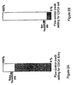
- FIG. 2A illustrates one embodiment of the entry threshold.
- the entry threshold 210 may be set to modify the bus mastering indicator to cause an exemplary CPU to enter into the C3 or C4 state even when there are pending incoherent transactions in the root complex device.
- the transactions may be intentionally held pending in the memory controller with no service attempted until the number of credits consumed exceeds or equals to the entry threshold 210 in order to defer asserting the bus mastering indicator to the CPU.
- the CPU has more opportunities to enter into either the C3 or C4 state to reduce average CPU power consumption.
- the entry threshold 210 may be set at 0% for highly performance sensitive applications, such as graphic applications.
- the entry threshold may be set at different values depending on the amount of charge remaining in one or more batteries of the system when the system is running solely on such batteries. It is noted that the tradeoff for lower CPU power consumption may be degraded CPU performance state. Furthermore, in one embodiment, a timer is used to qualify how long to stall servicing the initial pending transaction in order to mitigate the impact of the tradeoff on some latency sensitive applications. If the timer expires before the entry threshold 210 is reached, then the bus mastering indicator may be reset to allow the CPU to enter the C3 or C4 state for light traffic or idle cases.
- FIG. 1B shows a flow diagram of one embodiment of a process to manage power in a computer system:
- the process is performed by processing logic that may comprise hardware (e.g., circuitry, dedicated logic, etc.), software (such as is run on a general purpose computer system or a dedicated machine), or a combination of both.
- processing logic may receive a coherent transaction from a peripheral device (processing block 140). Examples of the peripheral device include an external graphic core, an Ethernet controller, etc.
- processing logic consumes a number of credits to reflect the portion of buffer taken up by the coherent transaction received (processing block 142).
- processing logic checks whether the total number of consumed credits for the coherent transactions exceeds or equals to an exit threshold (processing block 144). If the total number of the consumed credits exceeds or equals to the exit threshold, processing logic causes the CPU to exit from either the C3 or C4 state (processing block 150). Processing logic may send a signal to the CPU to instruct the CPU to exit from either the C3 or C4 state. After exiting from the C3 or C4 state, in one embodiment, the CPU enters the C0 state.
- processing logic checks whether a timer has expired (processing block 146). If the timer has expired, processing logic causes the CPU to exit from either the C3 or C4 state (processing block 150). Otherwise, processing logic queues up the transaction (processing block 148) and repeats processing block 140. Alternatively, processing logic may not check the timer at all and may simply queue up the transaction (processing block 148) and repeat processing block 140 upon the determination that the total number of consumed credits is below the exit threshold.
- Figure 2B illustrates one embodiment of the exit threshold.
- the exit threshold 250 is set to decide when to set the bus mastering indicator to cause an exemplary CPU to exit from either the C3 or C4 state. Transactions may be queued up when the CPU is in the C3 or C4 state to allow the CPU to spend a certain period of time in the C3 or C4 state in order to achieve a certain level of power saving. If the number of consumed credits is below the exit threshold 250, then the CPU is held off from being notified that an exit condition has occurred. In one embodiment, a timer is used to qualify how long to stall servicing the initial pending transactions if the applications are latency sensitive.
- the exit threshold 250 may be set at 0% in order to meet the performance specifications of such applications.
- the exit threshold 250 is set at different values depending on the remaining battery charge capacity in the system when the battery alone powers the system.
- the entry threshold substantially equals to the exit threshold.
- the entry and exit thresholds may be hardwired to a single value at 0%.
- the entry and exit thresholds are set at different values. For instance, the entry threshold may be higher than the exit threshold. Furthermore, allowing the entry and exit thresholds to be set at different values on the fly enables the CPU to adjust performance based on the remaining battery charge capacity.
- the CPU may modify the entry and exit behavior of the CPU adaptively through threshold modification. Adaptive modification of the entry and exit thresholds allows the CPU to steer away from frequent thrashing of low power states because of certain periodic traffic that may coincide with the timing of the C3 or C4 state entry decision. Another advantage is to provide for asymmetric entry and exit behavior to tune and increase the residency period of the CPU in either the C3 or C4 state.
- the CPU may take hundreds of microseconds to exit the C3 or C4 state, during which a phase lock loop of the CPU may consume twice the power consumed during the initial ten microseconds to spin up. Therefore, if the C3 or C4 residency of the CPU is less than the exit latency, the net effect may be little or negligible power saving, or worse, more power consumption.
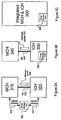
- Figures 3A - 3C illustrate various embodiments of chipset partitions in a computer system.
- Figure 3A shows a memory controller 310, an input/output controller 320, and power management circuitry 330.
- the power management circuitry 330 is outside of both the memory controller 310 and the input/output controller 320.
- the memory controller 310 is coupled to the input/output controller 320 via a link 315.
- the link 315 may include a digital media interface (DMI) link.
- the memory controller 310 is further coupled to one or more peripheral devices (not shown) via one or more buses or interconnects (not shown) that adopt a protocol with a credit-based flow control accounting scheme, such as, for example, PCI Express.
- DMI digital media interface
- the power management circuitry 330 communicates with the memory controller 310 and/or the input/output controller 320 via the sideband signals 332 and 334
- the sideband signals 332 and 334 indicate whether there is any bus mastering activity from a peripheral device, such as an advance graphic port (AGP).
- the sideband signals 332 and 334 are typically denoted as XX_BUSY.
- the sideband signal corresponding to the AGP is denoted as AGP_BUSY.
- the sideband signals may include one or more shared signals.
- one of the memory controller 310 and the input/output controller 320 acts as a central agent to roll up the bus mastering activity information through one or more message packets sent between the memory controller 310 and the input/output controller 320.
- the message packets may include DMI message packets 325.
- the central agent still communicates with the power management circuitry 330 via one of the sideband signals 334 and 332.
- FIG 3B shows an alternate embodiment of chipset partition in a computer system.
- the chipset in Figure 3B includes a memory controller 340 and an input/output controller 350 coupling to each other via a link 345, which may include a DMI link.
- a link 345 which may include a DMI link.
- the memory controller 340 is further coupled to a peripheral device (not shown) via an interconnect (not shown) adopting a credit-based flow control accounting scheme, such as, for example, PCI Express.
- the peripheral device may include an external graphic core, an Ethernet controller, etc.
- the input/output controller 350 includes power management circuitry 352 to monitor data traffic over the interconnect.
- the memory controller 340 Since the power management circuitry 352 is internal to the input/output controller 350, the memory controller 340 has to communicate to the input/output controller 350 on whether the peripheral device has any on-going traffic over the interconnect. In one embodiment, the memory controller 340 sets one or more bits in a message packet 347 sent via the link 345 to the input/output controller 350.
- the message packet 347 may be a DMI packet. Setting the bit(s) in the message packet 347 is also referred to as in-band virtualization of the bus mastering indicator signal, as opposed to the sideband signals (e.g., sideband signals 332 and 334 in Figure 3A ), because the signal is abstracted to eliminate the pin and connector infrastructure on both of the controllers 340 and 350.
- the power management circuitry 352 may also monitor the bus mastering activity from other peripheral devices (not shown) coupled to the input/output controller 350 via other interconnects (not shown).
- FIG. 3C shows an alternate embodiment of a chipset partition in a computer system.
- the chipset shown in Figure 3C includes an integrated memory and input/output controller 360.
- the integrated memory and input/output controller 360 includes internal power management circuitry 365. Since the power management circuitry 365 is part of the integrated controller 360, the bus mastering indications for peripheral devices coupled to the controller 360 may be internally registered through logic circuitry within the controller 360.
- FIG. 4 shows an exemplary embodiment of a computer system 400.
- the computer system 400 includes a central processing unit (CPU) 410, a memory controller (MCH) 420, a number of dual in-line memory modules (DIMMs) 425, a number of memory devices 427, a PCI Express graphic port 430, an input/output controller (ICH) 440, a number of Universal Serial Bus (USB) ports 445, an audio coder-decoder (AUDIO CODEC) 460, a Super Input/Output (Super I/O) 450, and a firmware hub (FWH) 470.
- CPU central processing unit
- MCH memory controller
- DIMMs dual in-line memory modules
- ICH input/output controller
- USB Universal Serial Bus
- AUDIO CODEC audio coder-decoder
- Super I/O Super I/O
- FWH firmware hub
- the CPU 410, the PCI Express graphic port 430, the DIMMs 425, and the ICH 440 are coupled to the MCH 420.
- the link 435 between the MCH 420 and the ICH 440 may include a DMI link.
- the MCH 420 routes data to and from the memory devices 427 via the DIMMs 425.
- the memory devices 427 may include various types of memories, such as, for example, dynamic random access memory (DRAM), synchronous dynamic random access memory (SDRAM), double data rate (DDR) SDRAM, or flash memory.
- each of the DIMMs 425 is mounted on the same motherboard (not shown) via a DIMM connector (not shown) in order to couple to the MCH 420.
- the USB ports 445, the AUDIO CODEC 460, and the Super I/O 450 are coupled to the ICH 440.
- the Super I/O 450 may be further coupled to a firmware hub 470, a floppy disk drive 451, data input devices 453, such as, a keyboard, a mouse, etc., a number of serial ports 455, and a number of parallel ports 457.
- the ICH 440 includes power management circuitry 442 to monitor data traffic over various interconnects coupling the ICH 440 and the MCH 420 to the peripheral devices, such as, for example, the PCI Express graphic port 430.
- the power management circuitry 442 may generate a bus mastering indicator to be sent as a virtualized signal within a message packet 437 from the MCH 420 to the ICH 440 via the link 435.
- the MCH 420 and the ICH 440 may be integrated into a single controller with power management circuitry such that the bus mastering indicator may be internally registered through logic.
- the MCH 420 and the ICH 440 remain as separate devices and the power management circuitry is external to both of the MCH 420 and the ICH 440.
- Either one of the MCH 420 and the ICH 440 may act as a central agent to roll up information of bus traffic from the peripheral devices in the system 400 from the other controller using message packets sent between the controllers 420 and 440.
- the central agent may communicate the information to the external power management circuitry via one or more sideband signals.
- any or all of the components and the associated hardware illustrated in Figure 4 may be used in various embodiments of the computer system 400. However, it should be appreciated that other configuration of the computer system may include one or more additional devices not shown in Figure 4 . Furthermore, one should appreciate that the technique disclosed is applicable to different types of system environment, such as a multi-drop environment or a point-to-point environment Likewise, the disclosed technique is applicable to both mobile and desktop computing systems.
Landscapes
- Engineering & Computer Science (AREA)
- Theoretical Computer Science (AREA)
- Physics & Mathematics (AREA)
- General Engineering & Computer Science (AREA)
- General Physics & Mathematics (AREA)
- Power Sources (AREA)
Claims (20)
- Verfahren zum Power-Management in einem System (400), das einen Prozessor (410) aufweist, der einen Cache-Speicher aufweist, das Verfahren aufweisend:Überwachen von Transaktionen über eine Zusammenschaltung, die ein Chipsatz-Gerät (420) und ein peripheres Gerät (430) im System verkoppelt, wobei die Transaktionen zwischen dem peripheren Gerät und dem Chipsatz-Gerät gemäß einem Ablaufsteuerprotokoll übertragen werden, das es dem Chipsatz-Gerät ermöglicht, die Transaktionen zu verfolgen;Bewirken (150), dass ein Prozessor (410) im System aus einem ersten Leistungszustand, in dem Snooping von Bus-Master eingerichtetem Speicherverkehr abgeschaltet ist, in einen zweiten Leistungszustand übergeht, in dem derartiges Snooping ermöglicht ist, wenn eine Anzahl verbrauchter Guthaben für mehrere kohärente Transaktionen, die in einem Zwischenspeicher des Chipsatz-Geräts anhängig sind, eine erste Schwelle (250) übersteigt; undEntwerten (129) eines Indikators innerhalb eines Nachrichtenpakets (437), wodurch dem Prozessor das Übergehen in den ersten Leistungszustand aus dem zweiten Leistungszustand in Reaktion auf eine Anforderung (101) vom Prozessor zum Übergehen in den ersten Leistungszustand ermöglicht wird, wenn eine Anzahl verbrauchter Guthaben für mehrere inkohärente Transaktionen, die im Zwischenspeicher des Chipsatz-Geräts anhängig sind, eine zweite Schwelle (210) übersteigt, wobei die Anzahl verbrauchter Guthaben für die mehreren kohärenten Transaktionen, die im Zwischenspeicher anhängig sind, den Anteil des Zwischenspeichers wiedergibt, der durch die mehreren kohärenten Transaktionen belegt ist, und die Anzahl verbrauchter Guthaben für die mehreren inkohärenten Transaktionen, die im Zwischenspeicher anhängig sind, den Anteil des Zwischenspeichers wiedergibt, der durch die mehreren inkohärenten Transaktionen belegt ist.
- Verfahren nach Anspruch 1, ferner aufweisend:Bestimmen (146), ob ein vorgegebener Zeitraum verstrichen ist, wenn die Anzahl verbrauchter Guthaben für die mehreren kohärenten Transaktionen, die im Zwischenspeicher des Chipsatz-Geräts anhängig sind, die erste Schwelle (250) nicht übersteigt; undBewirken (150), dass der Prozessor (410) aus dem ersten Leistungszustand in den zweiten Leistungszustand übergeht, wenn der vorgegebene Zeitraum verstrichen ist.
- Verfahren nach Anspruch 1, ferner aufweisend:Geltendmachen (130) des Indikators innerhalb des Nachrichtenpakets (437), um zu verhindern, dass der Prozessor (410) in den ersten Leistungszustand übergeht, wenn die Anzahl verbrauchter Guthaben für die mehreren inkohärenten Transaktionen, die im Zwischenspeicher des Chipsatz-Geräts anhängig sind, unterhalb der zweiten Schwelle (210) liegt.
- Verfahren nach Anspruch 1, ferner aufweisend:Bestimmen (122), ob ein zweiter vorgegebener Zeitraum verstrichen ist, wenn die Anzahl verbrauchter Guthaben für die mehreren inkohärenten Transaktionen, die im Zwischenspeicher des Chipsatz-Geräts anhängig sind, unterhalb der zweiten Schwelle (210) liegt; undEntwerten (129) des Indikators innerhalb des Nachrichtenpakets (437), um es dem Prozessor (410) zu ermöglichen, aus dem ersten Leistungszustand in den zweiten Leistungszustand überzugehen, wenn der zweite vorgegebene Zeitraum verstrichen ist.
- Verfahren nach Anspruch 1, wobei die erste Schwelle (250) gleich der zweiten Schwelle (210) ist.
- Verfahren nach Anspruch 1, wobei die erste Schwelle (250) niedriger als die zweite Schwelle (210) ist.
- Verfahren nach Anspruch 1, wobei das Ablaufsteuerprotokoll "Peripheral Component Interconnect (PCI) Express" ist.
- Verfahren nach Anspruch 1, wobei das Chipsatz-Gerät eine Speichersteuerung (420) aufweist.
- Verfahren nach Anspruch 1, wobei das Chipsatz-Gerät eine Ein-/Ausgabe-Steuerung (440) aufweist.
- Rechensystem (400), aufweisend:einen Prozessor (410), der einen Cache-Speicher aufweist;ein Root-Complex-Gerät (420);ein peripheres Gerät (430);eine Vorrichtung (440), die Power-Management-Schaltungen (442) aufweist, welche an das Root-Complex-Gerät (420) gekoppelt sind, wobei die Power-Management-Schaltungen (442) zum Überwachen von Transaktionen über eine Zusammenschaltung, die das Root-Complex-Gerät (420) und das periphere Gerät (430) verkoppelt, konfiguriert sind, wobei die Transaktionen zwischen dem peripheren Gerät (430) und dem Root-Complex-Gerät (420) gemäß einem Ablaufsteuerprotokoll übertragen werden, um es dem Root-Complex-Gerät zu ermöglichen, die übertragenen Transaktionen zu verfolgen; unddadurch gekennzeichnet, dass die Vorrichtung Folgendes aufweist:eine digitale Medienschnittstelle (435), die an das Root-Complex-Gerät (420) gekoppelt ist, zum Senden eines ersten Nachrichtenpakets (437) an das Root-Complex-Gerät (420), um zu bewirken (150), dass der Prozessor (410) aus einem ersten Leistungszustand, in dem Snooping von Bus-Master eingerichtetem Speicherverkehr abgeschaltet ist, in einen zweiten Leistungszustand übergeht, in dem derartiges Snooping ermöglicht ist, wenn eine Anzahl verbrauchter Guthaben für mehrere kohärente Transaktionen, die in einem Zwischenspeicher des Root-Complex-Geräts (420) anhängig sind, eine erste Schwelle (250) übersteigt, wobei in Reaktion auf eine Anforderung vom Prozessor (410) zum Übergehen in den ersten Leistungszustand aus dem zweiten Leistungszustand die Power-Management-Schaltungen (442) einen Indikator innerhalb eines zweiten Nachrichtenpakets entwerten (129), wodurch dem Prozessor das Übergehen in den ersten Leistungszustand ermöglicht wird, wenn eine Anzahl verbrauchter Guthaben für mehrere inkohärente Transaktionen, die im Zwischenspeicher des Root-Complex-Geräts anhängig sind, eine zweite Schwelle (210) übersteigt, wobei die Anzahl verbrauchter Guthaben für die mehreren kohärenten Transaktionen, die im Zwischenspeicher anhängig sind, den Anteil des Zwischenspeichers wiedergibt, der durch die mehreren kohärenten Transaktionen belegt ist, und die Anzahl verbrauchter Guthaben für die mehreren inkohärenten Transaktionen, die im Zwischenspeicher anhängig sind, den Anteil des Zwischenspeichers wiedergibt, der durch die mehreren inkohärenten Transaktionen belegt ist.
- Rechensystem nach Anspruch 10, wobei in Reaktion auf die Anforderung (101) vom Prozessor (410) die Power-Management-Schaltungen (442) den Indikator innerhalb des zweiten Nachrichtenpakets geltend machen (130), um zu verhindern, dass der Prozessor (410) in den ersten Leistungszustand eintritt, wenn die Anzahl verbrauchter Guthaben für die mehreren inkohärenten Transaktionen, die im Zwischenspeicher des Root-Complex-Geräts anhängig sind, unterhalb der zweiten Schwelle (210) liegt.
- Rechensystem nach Anspruch 11, wobei die Vorrichtung ferner einen Timer aufweist, wobei die Power-Management-Schaltungen (442) den Indikator innerhalb des zweiten Nachrichtenpakets geltend machen (130), um zu verhindern, dass der Prozessor (410) in den ersten Leistungszustand eintritt, wenn der Timer abgelaufen ist.
- Rechensystem nach Anspruch 11, wobei die erste Schwelle (250) gleich der zweiten Schwelle (210) ist.
- Rechensystem nach Anspruch 10, wobei das Ablaufsteuerprotokoll ein guthabenbasiertes Ablaufsteuerverrechnungsschema enthält.
- Rechensystem (400), aufweisend:einen Prozessor (410), der einen Cache-Speicher aufweist;ein peripheres Gerät (430);eine Speichersteuerung (420), die an das periphere Gerät (430) gekoppelt ist;Power-Management-Schaltungen (442), die zum Überwachen von Transaktionen zwischen dem peripheren Gerät (430) und der Speichersteuerung (420) an die Speichersteuerung gekoppelt sind;gekennzeichnet durch:eine Ein-/Ausgabe-Steuerung (450), die an die Speichersteuerung (420) gekoppelt ist, wobei die Speichersteuerung (420) zum Empfangen eines ersten Nachrichtenpakets (437) geeignet ist, wodurch ermöglicht ist (129), dass der Prozessor (410) im Rechensystem (400) in einen ersten Leistungszustand, in dem Snooping von Bus-Master eingerichtetem Speicherverkehr abgeschaltet ist, aus einem zweiten Leistungszustand übergeht, in dem derartiges Snooping ermöglicht ist, in Reaktion auf eine Anforderung (101) vom Prozessor (410), in den ersten Leistungszustand überzugehen, wenn eine Anzahl verbrauchter Guthaben für mehrere inkohärente Transaktionen, die in einem Zwischenspeicher der Speichersteuerung (420) anhängig sind, eine Eintrittsschwelle (210) übersteigt, um zu verhindern (130), dass der Prozessor (410) in den ersten Leistungszustand übergeht, wenn die Anzahl verbrauchter Guthaben für die mehreren inkohärenten Transaktionen unterhalb der Eintrittsschwelle (210) liegt, und um zu bewirken (150), dass der Prozessor (410) aus dem ersten Leistungszustand in den zweiten Leistungszustand übergeht, wenn eine Anzahl verbrauchter Guthaben für mehrere kohärente Transaktionen, die im Zwischenspeicher der Speichersteuerung anhängig sind, eine Austrittsschwelle (250) übersteigt, wobei die Anzahl verbrauchter Guthaben für die mehreren kohärenten Transaktionen, die im Zwischenspeicher anhängig sind, den Anteil des Zwischenspeichers wiedergibt, der durch die mehreren kohärenten Transaktionen belegt ist, und die Anzahl verbrauchter Guthaben für die mehreren inkohärenten Transaktionen, die im Zwischenspeicher anhängig sind, den Anteil des Zwischenspeichers wiedergibt, der durch die mehreren inkohärenten Transaktionen belegt ist.
- Rechensystem nach Anspruch 15, wobei die Eintrittsschwelle (210) gleich der Austrittschwelle (250) ist.
- Rechensystem nach Anspruch 15, wobei die Eintritts- und Austrittsschwelle (210, 250) adaptiv modifizierbar sind.
- Rechensystem nach Anspruch 15, wobei das periphere Gerät (430) an die Speichersteuerung (420) über eine Zusammenschaltung gekoppelt ist, die ein guthabenbasiertes Ablaufsteuerverrechnungsschema annimmt.
- Rechensystem nach Anspruch 15, wobei das periphere Gerät (430) über einen Bus an die Speichersteuerung (420) gekoppelt ist.
- Rechensystem nach einem der Ansprüche 10 bis 14, wobei das Root-Complex-Gerät (420) eine Speichersteuerung (420) aufweist; wobei das periphere Gerät (430) einen Grafikchip (430) aufweist; und wobei die Vorrichtung (440) eine Ein-/Ausgabe-Steuerung (440) aufweist.
Applications Claiming Priority (2)
| Application Number | Priority Date | Filing Date | Title |
|---|---|---|---|
| US10/749,855 US7237131B2 (en) | 2003-12-30 | 2003-12-30 | Transaction-based power management in a computer system |
| PCT/US2004/043675 WO2005066743A2 (en) | 2003-12-30 | 2004-12-23 | A method and an apparatus for power management in a computer system |
Publications (2)
| Publication Number | Publication Date |
|---|---|
| EP1702253A2 EP1702253A2 (de) | 2006-09-20 |
| EP1702253B1 true EP1702253B1 (de) | 2016-06-29 |
Family
ID=34711148
Family Applications (1)
| Application Number | Title | Priority Date | Filing Date |
|---|---|---|---|
| EP04815690.5A Expired - Lifetime EP1702253B1 (de) | 2003-12-30 | 2004-12-23 | Verfahren und vorrichtung zum power-management in einem computersystem |
Country Status (7)
| Country | Link |
|---|---|
| US (1) | US7237131B2 (de) |
| EP (1) | EP1702253B1 (de) |
| JP (1) | JP4376907B2 (de) |
| KR (1) | KR100798980B1 (de) |
| CN (1) | CN100498652C (de) |
| TW (1) | TWI266183B (de) |
| WO (1) | WO2005066743A2 (de) |
Families Citing this family (40)
| Publication number | Priority date | Publication date | Assignee | Title |
|---|---|---|---|---|
| US7178045B2 (en) * | 2003-12-30 | 2007-02-13 | Intel Corporation | Optimizing exit latency from an active power management state |
| JP4316399B2 (ja) * | 2004-02-18 | 2009-08-19 | インターナショナル・ビジネス・マシーンズ・コーポレーション | プログラム、記録媒体、制御方法、及び情報処理装置 |
| JP4189882B2 (ja) * | 2004-05-11 | 2008-12-03 | インターナショナル・ビジネス・マシーンズ・コーポレーション | 記録媒体、情報処理装置、制御方法、及びプログラム |
| US7353414B2 (en) * | 2005-03-30 | 2008-04-01 | Intel Corporation | Credit-based activity regulation within a microprocessor based on an allowable activity level |
| JP2006338380A (ja) * | 2005-06-02 | 2006-12-14 | Toshiba Corp | 情報処理装置およびその制御方法 |
| US20060277126A1 (en) * | 2005-06-06 | 2006-12-07 | Intel Corporation | Ring credit management |
| US7924708B2 (en) * | 2005-12-13 | 2011-04-12 | Intel Corporation | Method and apparatus for flow control initialization |
| US7752473B1 (en) * | 2006-03-20 | 2010-07-06 | Intel Corporation | Providing a deterministic idle time window for an idle state of a device |
| US20070260780A1 (en) * | 2006-04-11 | 2007-11-08 | Nokia Corporation | Media subsystem, method and computer program product for adaptive media buffering |
| US7689847B2 (en) * | 2006-06-13 | 2010-03-30 | Via Technologies, Inc. | Method for increasing the data processing capability of a computer system |
| US7783905B2 (en) * | 2006-06-13 | 2010-08-24 | Via Technologies Inc. | Method for reducing power consumption of a computer system in the working state |
| US7895456B2 (en) * | 2006-11-12 | 2011-02-22 | Microsemi Corp. - Analog Mixed Signal Group Ltd | Reduced guard band for power over Ethernet |
| US7734942B2 (en) * | 2006-12-28 | 2010-06-08 | Intel Corporation | Enabling idle states for a component associated with an interconnect |
| US7774626B2 (en) * | 2007-03-29 | 2010-08-10 | Intel Corporation | Method to control core duty cycles using low power modes |
| US8527709B2 (en) * | 2007-07-20 | 2013-09-03 | Intel Corporation | Technique for preserving cached information during a low power mode |
| US8156353B2 (en) * | 2007-09-17 | 2012-04-10 | Intel Corporation | Techniques for communications power management based on system states |
| US8386806B2 (en) * | 2007-12-17 | 2013-02-26 | Intel Corporation | Integrated power management logic |
| US8806258B2 (en) * | 2008-09-30 | 2014-08-12 | Intel Corporation | Platform communication protocol |
| US8019920B2 (en) * | 2008-10-01 | 2011-09-13 | Hewlett-Packard Development Company, L.P. | Method to improve operating performance of a computing device |
| US8627014B2 (en) * | 2008-12-30 | 2014-01-07 | Intel Corporation | Memory model for hardware attributes within a transactional memory system |
| US9785462B2 (en) | 2008-12-30 | 2017-10-10 | Intel Corporation | Registering a user-handler in hardware for transactional memory event handling |
| US8799582B2 (en) * | 2008-12-30 | 2014-08-05 | Intel Corporation | Extending cache coherency protocols to support locally buffered data |
| US8156275B2 (en) | 2009-05-13 | 2012-04-10 | Apple Inc. | Power managed lock optimization |
| KR101282199B1 (ko) * | 2009-11-19 | 2013-07-04 | 한국전자통신연구원 | 클러스터 시스템의 전력 제어 장치 및 방법 |
| US8850250B2 (en) * | 2010-06-01 | 2014-09-30 | Intel Corporation | Integration of processor and input/output hub |
| US8782456B2 (en) | 2010-06-01 | 2014-07-15 | Intel Corporation | Dynamic and idle power reduction sequence using recombinant clock and power gating |
| US9146610B2 (en) | 2010-09-25 | 2015-09-29 | Intel Corporation | Throttling integrated link |
| EP2673684B1 (de) | 2011-02-08 | 2019-06-05 | NXP USA, Inc. | Integrierte schaltvorrichtung, leistungsverwaltungsmodul und verfahren zur bereitstellung von leistungsverwaltung |
| US8862906B2 (en) * | 2011-04-01 | 2014-10-14 | Intel Corporation | Control of platform power consumption using coordination of platform power management and display power management |
| JP5791397B2 (ja) * | 2011-07-07 | 2015-10-07 | ルネサスエレクトロニクス株式会社 | デバイスコントローラ、usbデバイスコントローラ及び電力制御方法 |
| KR101380452B1 (ko) * | 2012-08-14 | 2014-04-14 | 한국과학기술원 | 버퍼리스 온칩 네트워크의 전력 소모 감소를 위한 목적지 기반 크레딧 흐름 제어 방법 및 장치 |
| US9116694B2 (en) * | 2012-09-26 | 2015-08-25 | Intel Corporation | Efficient low power exit sequence for peripheral devices |
| US20140095801A1 (en) * | 2012-09-28 | 2014-04-03 | Devadatta V. Bodas | System and method for retaining coherent cache contents during deep power-down operations |
| KR20140089749A (ko) | 2013-01-07 | 2014-07-16 | 한국전자통신연구원 | 클러스터의 부하 할당 제어 장치 및 그 방법 |
| JP2016523399A (ja) * | 2013-06-28 | 2016-08-08 | インテル コーポレイション | エネルギー効率的なモバイルプラットフォームのための適応的割り込みコアレッシング |
| US9541987B2 (en) * | 2013-06-28 | 2017-01-10 | Intel Corporation | Generic host-based controller latency method and appartus |
| US9880601B2 (en) | 2014-12-24 | 2018-01-30 | Intel Corporation | Method and apparatus to control a link power state |
| US10754410B2 (en) * | 2018-11-09 | 2020-08-25 | Monolithic Power Systems, Inc. | System and method for standby mode operation of power management system |
| CN110990332A (zh) * | 2019-12-04 | 2020-04-10 | 合肥市卓怡恒通信息安全有限公司 | 基于申威处理器的服务器主板 |
| US11513973B2 (en) * | 2019-12-20 | 2022-11-29 | Advanced Micro Devices, Inc. | Arbitration scheme for coherent and non-coherent memory requests |
Family Cites Families (13)
| Publication number | Priority date | Publication date | Assignee | Title |
|---|---|---|---|---|
| US5721935A (en) * | 1995-12-20 | 1998-02-24 | Compaq Computer Corporation | Apparatus and method for entering low power mode in a computer system |
| US5740454A (en) * | 1995-12-20 | 1998-04-14 | Compaq Computer Corporation | Circuit for setting computer system bus signals to predetermined states in low power mode |
| US6085330A (en) * | 1998-04-07 | 2000-07-04 | Advanced Micro Devices, Inc. | Control circuit for switching a processor between multiple low power states to allow cache snoops |
| US6128745A (en) * | 1998-05-28 | 2000-10-03 | Phoenix Technologies Ltd. | Power management inactivity monitoring using software threads |
| US6021506A (en) * | 1998-07-31 | 2000-02-01 | Intel Corporation | Method and apparatus for stopping a bus clock while there are no activities on a bus |
| US6820169B2 (en) * | 2001-09-25 | 2004-11-16 | Intel Corporation | Memory control with lookahead power management |
| US7260106B2 (en) * | 2002-01-24 | 2007-08-21 | Intel Corporation | Method and apparatus for managing energy usage of processors while executing protocol state machines |
| EP1338948A1 (de) | 2002-02-25 | 2003-08-27 | Hewlett Packard Company, a Delaware Corporation | Taktsteuerungsanordnung für ein Rechnersystem |
| US7103064B2 (en) * | 2003-01-21 | 2006-09-05 | Nextio Inc. | Method and apparatus for shared I/O in a load/store fabric |
| US7219183B2 (en) * | 2003-01-21 | 2007-05-15 | Nextio, Inc. | Switching apparatus and method for providing shared I/O within a load-store fabric |
| US20040212678A1 (en) * | 2003-04-25 | 2004-10-28 | Cooper Peter David | Low power motion detection system |
| US7546418B2 (en) * | 2003-08-20 | 2009-06-09 | Dell Products L.P. | System and method for managing power consumption and data integrity in a computer system |
| US7782325B2 (en) * | 2003-10-22 | 2010-08-24 | Alienware Labs Corporation | Motherboard for supporting multiple graphics cards |
-
2003
- 2003-12-30 US US10/749,855 patent/US7237131B2/en not_active Expired - Fee Related
-
2004
- 2004-12-23 EP EP04815690.5A patent/EP1702253B1/de not_active Expired - Lifetime
- 2004-12-23 WO PCT/US2004/043675 patent/WO2005066743A2/en not_active Ceased
- 2004-12-23 KR KR1020067013281A patent/KR100798980B1/ko not_active Expired - Fee Related
- 2004-12-23 CN CNB2004800395405A patent/CN100498652C/zh not_active Expired - Fee Related
- 2004-12-23 JP JP2006547484A patent/JP4376907B2/ja not_active Expired - Fee Related
- 2004-12-23 TW TW093140273A patent/TWI266183B/zh not_active IP Right Cessation
Also Published As
| Publication number | Publication date |
|---|---|
| TW200530806A (en) | 2005-09-16 |
| KR100798980B1 (ko) | 2008-01-28 |
| KR20060111658A (ko) | 2006-10-27 |
| TWI266183B (en) | 2006-11-11 |
| EP1702253A2 (de) | 2006-09-20 |
| CN100498652C (zh) | 2009-06-10 |
| US7237131B2 (en) | 2007-06-26 |
| CN1902566A (zh) | 2007-01-24 |
| WO2005066743A3 (en) | 2005-12-08 |
| JP2007517332A (ja) | 2007-06-28 |
| WO2005066743A2 (en) | 2005-07-21 |
| JP4376907B2 (ja) | 2009-12-02 |
| US20050149768A1 (en) | 2005-07-07 |
Similar Documents
| Publication | Publication Date | Title |
|---|---|---|
| EP1702253B1 (de) | Verfahren und vorrichtung zum power-management in einem computersystem | |
| US8656198B2 (en) | Method and apparatus for memory power management | |
| US5692202A (en) | System, apparatus, and method for managing power in a computer system | |
| US6820209B1 (en) | Power managed graphics controller | |
| US7966506B2 (en) | Saving power in a computer system | |
| US8365001B2 (en) | Method and apparatus for adaptive power management of memory subsystem | |
| US7496777B2 (en) | Power throttling in a memory system | |
| US6971033B2 (en) | Method and apparatus for improving bus master performance | |
| CN102646446B (zh) | 硬件动态高速缓存电源管理 | |
| US7603504B2 (en) | Reducing core wake-up latency in a computer system | |
| US10409357B1 (en) | Command-oriented low power control method of high-bandwidth-memory system | |
| US7689849B2 (en) | Reduction of power consumption by throttling processor requests | |
| US20140208144A1 (en) | Method and Apparatus for Adaptive Power Management of Memory Subsystem | |
| US7340550B2 (en) | USB schedule prefetcher for low power | |
| EP1573491B1 (de) | Vorrichtung und verfahren zur datenbusleistungssteuerung | |
| EP1570335B1 (de) | Verfahren und methode zur steuerung der adressbus-spannungsversorgung | |
| HK1075949B (en) | An apparatus and method for address bus power control |
Legal Events
| Date | Code | Title | Description |
|---|---|---|---|
| PUAI | Public reference made under article 153(3) epc to a published international application that has entered the european phase |
Free format text: ORIGINAL CODE: 0009012 |
|
| 17P | Request for examination filed |
Effective date: 20060727 |
|
| AK | Designated contracting states |
Kind code of ref document: A2 Designated state(s): AT BE BG CH CY CZ DE DK EE ES FI FR GB GR HU IE IS IT LI LT LU MC NL PL PT RO SE SI SK TR |
|
| DAX | Request for extension of the european patent (deleted) | ||
| 17Q | First examination report despatched |
Effective date: 20070424 |
|
| GRAP | Despatch of communication of intention to grant a patent |
Free format text: ORIGINAL CODE: EPIDOSNIGR1 |
|
| INTG | Intention to grant announced |
Effective date: 20160119 |
|
| GRAS | Grant fee paid |
Free format text: ORIGINAL CODE: EPIDOSNIGR3 |
|
| GRAA | (expected) grant |
Free format text: ORIGINAL CODE: 0009210 |
|
| AK | Designated contracting states |
Kind code of ref document: B1 Designated state(s): AT BE BG CH CY CZ DE DK EE ES FI FR GB GR HU IE IS IT LI LT LU MC NL PL PT RO SE SI SK TR |
|
| REG | Reference to a national code |
Ref country code: GB Ref legal event code: FG4D |
|
| REG | Reference to a national code |
Ref country code: CH Ref legal event code: EP |
|
| REG | Reference to a national code |
Ref country code: AT Ref legal event code: REF Ref document number: 809585 Country of ref document: AT Kind code of ref document: T Effective date: 20160715 |
|
| REG | Reference to a national code |
Ref country code: IE Ref legal event code: FG4D |
|
| REG | Reference to a national code |
Ref country code: DE Ref legal event code: R096 Ref document number: 602004049521 Country of ref document: DE |
|
| REG | Reference to a national code |
Ref country code: NL Ref legal event code: FP |
|
| REG | Reference to a national code |
Ref country code: LT Ref legal event code: MG4D |
|
| PG25 | Lapsed in a contracting state [announced via postgrant information from national office to epo] |
Ref country code: FI Free format text: LAPSE BECAUSE OF FAILURE TO SUBMIT A TRANSLATION OF THE DESCRIPTION OR TO PAY THE FEE WITHIN THE PRESCRIBED TIME-LIMIT Effective date: 20160629 Ref country code: LT Free format text: LAPSE BECAUSE OF FAILURE TO SUBMIT A TRANSLATION OF THE DESCRIPTION OR TO PAY THE FEE WITHIN THE PRESCRIBED TIME-LIMIT Effective date: 20160629 |
|
| PG25 | Lapsed in a contracting state [announced via postgrant information from national office to epo] |
Ref country code: SE Free format text: LAPSE BECAUSE OF FAILURE TO SUBMIT A TRANSLATION OF THE DESCRIPTION OR TO PAY THE FEE WITHIN THE PRESCRIBED TIME-LIMIT Effective date: 20160629 Ref country code: GR Free format text: LAPSE BECAUSE OF FAILURE TO SUBMIT A TRANSLATION OF THE DESCRIPTION OR TO PAY THE FEE WITHIN THE PRESCRIBED TIME-LIMIT Effective date: 20160930 |
|
| REG | Reference to a national code |
Ref country code: AT Ref legal event code: MK05 Ref document number: 809585 Country of ref document: AT Kind code of ref document: T Effective date: 20160629 |
|
| PG25 | Lapsed in a contracting state [announced via postgrant information from national office to epo] |
Ref country code: IT Free format text: LAPSE BECAUSE OF FAILURE TO SUBMIT A TRANSLATION OF THE DESCRIPTION OR TO PAY THE FEE WITHIN THE PRESCRIBED TIME-LIMIT Effective date: 20160629 Ref country code: EE Free format text: LAPSE BECAUSE OF FAILURE TO SUBMIT A TRANSLATION OF THE DESCRIPTION OR TO PAY THE FEE WITHIN THE PRESCRIBED TIME-LIMIT Effective date: 20160629 Ref country code: SK Free format text: LAPSE BECAUSE OF FAILURE TO SUBMIT A TRANSLATION OF THE DESCRIPTION OR TO PAY THE FEE WITHIN THE PRESCRIBED TIME-LIMIT Effective date: 20160629 Ref country code: IS Free format text: LAPSE BECAUSE OF FAILURE TO SUBMIT A TRANSLATION OF THE DESCRIPTION OR TO PAY THE FEE WITHIN THE PRESCRIBED TIME-LIMIT Effective date: 20161029 Ref country code: RO Free format text: LAPSE BECAUSE OF FAILURE TO SUBMIT A TRANSLATION OF THE DESCRIPTION OR TO PAY THE FEE WITHIN THE PRESCRIBED TIME-LIMIT Effective date: 20160629 Ref country code: CZ Free format text: LAPSE BECAUSE OF FAILURE TO SUBMIT A TRANSLATION OF THE DESCRIPTION OR TO PAY THE FEE WITHIN THE PRESCRIBED TIME-LIMIT Effective date: 20160629 |
|
| PG25 | Lapsed in a contracting state [announced via postgrant information from national office to epo] |
Ref country code: AT Free format text: LAPSE BECAUSE OF FAILURE TO SUBMIT A TRANSLATION OF THE DESCRIPTION OR TO PAY THE FEE WITHIN THE PRESCRIBED TIME-LIMIT Effective date: 20160629 Ref country code: BE Free format text: LAPSE BECAUSE OF FAILURE TO SUBMIT A TRANSLATION OF THE DESCRIPTION OR TO PAY THE FEE WITHIN THE PRESCRIBED TIME-LIMIT Effective date: 20160629 Ref country code: PL Free format text: LAPSE BECAUSE OF FAILURE TO SUBMIT A TRANSLATION OF THE DESCRIPTION OR TO PAY THE FEE WITHIN THE PRESCRIBED TIME-LIMIT Effective date: 20160629 Ref country code: PT Free format text: LAPSE BECAUSE OF FAILURE TO SUBMIT A TRANSLATION OF THE DESCRIPTION OR TO PAY THE FEE WITHIN THE PRESCRIBED TIME-LIMIT Effective date: 20161031 Ref country code: ES Free format text: LAPSE BECAUSE OF FAILURE TO SUBMIT A TRANSLATION OF THE DESCRIPTION OR TO PAY THE FEE WITHIN THE PRESCRIBED TIME-LIMIT Effective date: 20160629 |
|
| REG | Reference to a national code |
Ref country code: DE Ref legal event code: R097 Ref document number: 602004049521 Country of ref document: DE |
|
| PLBE | No opposition filed within time limit |
Free format text: ORIGINAL CODE: 0009261 |
|
| STAA | Information on the status of an ep patent application or granted ep patent |
Free format text: STATUS: NO OPPOSITION FILED WITHIN TIME LIMIT |
|
| PG25 | Lapsed in a contracting state [announced via postgrant information from national office to epo] |
Ref country code: DK Free format text: LAPSE BECAUSE OF FAILURE TO SUBMIT A TRANSLATION OF THE DESCRIPTION OR TO PAY THE FEE WITHIN THE PRESCRIBED TIME-LIMIT Effective date: 20160629 |
|
| 26N | No opposition filed |
Effective date: 20170330 |
|
| REG | Reference to a national code |
Ref country code: CH Ref legal event code: PL |
|
| PG25 | Lapsed in a contracting state [announced via postgrant information from national office to epo] |
Ref country code: SI Free format text: LAPSE BECAUSE OF FAILURE TO SUBMIT A TRANSLATION OF THE DESCRIPTION OR TO PAY THE FEE WITHIN THE PRESCRIBED TIME-LIMIT Effective date: 20160629 Ref country code: BG Free format text: LAPSE BECAUSE OF FAILURE TO SUBMIT A TRANSLATION OF THE DESCRIPTION OR TO PAY THE FEE WITHIN THE PRESCRIBED TIME-LIMIT Effective date: 20160929 |
|
| PG25 | Lapsed in a contracting state [announced via postgrant information from national office to epo] |
Ref country code: MC Free format text: LAPSE BECAUSE OF FAILURE TO SUBMIT A TRANSLATION OF THE DESCRIPTION OR TO PAY THE FEE WITHIN THE PRESCRIBED TIME-LIMIT Effective date: 20160629 |
|
| REG | Reference to a national code |
Ref country code: FR Ref legal event code: ST Effective date: 20170831 |
|
| REG | Reference to a national code |
Ref country code: IE Ref legal event code: MM4A |
|
| PG25 | Lapsed in a contracting state [announced via postgrant information from national office to epo] |
Ref country code: FR Free format text: LAPSE BECAUSE OF NON-PAYMENT OF DUE FEES Effective date: 20170102 Ref country code: CH Free format text: LAPSE BECAUSE OF NON-PAYMENT OF DUE FEES Effective date: 20161231 Ref country code: LU Free format text: LAPSE BECAUSE OF NON-PAYMENT OF DUE FEES Effective date: 20161223 Ref country code: LI Free format text: LAPSE BECAUSE OF NON-PAYMENT OF DUE FEES Effective date: 20161231 |
|
| PG25 | Lapsed in a contracting state [announced via postgrant information from national office to epo] |
Ref country code: IE Free format text: LAPSE BECAUSE OF NON-PAYMENT OF DUE FEES Effective date: 20161223 |
|
| PGFP | Annual fee paid to national office [announced via postgrant information from national office to epo] |
Ref country code: NL Payment date: 20171213 Year of fee payment: 14 |
|
| PG25 | Lapsed in a contracting state [announced via postgrant information from national office to epo] |
Ref country code: CY Free format text: LAPSE BECAUSE OF FAILURE TO SUBMIT A TRANSLATION OF THE DESCRIPTION OR TO PAY THE FEE WITHIN THE PRESCRIBED TIME-LIMIT Effective date: 20160629 Ref country code: HU Free format text: LAPSE BECAUSE OF FAILURE TO SUBMIT A TRANSLATION OF THE DESCRIPTION OR TO PAY THE FEE WITHIN THE PRESCRIBED TIME-LIMIT; INVALID AB INITIO Effective date: 20041223 |
|
| PG25 | Lapsed in a contracting state [announced via postgrant information from national office to epo] |
Ref country code: TR Free format text: LAPSE BECAUSE OF FAILURE TO SUBMIT A TRANSLATION OF THE DESCRIPTION OR TO PAY THE FEE WITHIN THE PRESCRIBED TIME-LIMIT Effective date: 20160629 |
|
| PGFP | Annual fee paid to national office [announced via postgrant information from national office to epo] |
Ref country code: DE Payment date: 20181211 Year of fee payment: 15 |
|
| REG | Reference to a national code |
Ref country code: NL Ref legal event code: MM Effective date: 20190101 |
|
| PG25 | Lapsed in a contracting state [announced via postgrant information from national office to epo] |
Ref country code: NL Free format text: LAPSE BECAUSE OF NON-PAYMENT OF DUE FEES Effective date: 20190101 |
|
| REG | Reference to a national code |
Ref country code: DE Ref legal event code: R119 Ref document number: 602004049521 Country of ref document: DE |
|
| PG25 | Lapsed in a contracting state [announced via postgrant information from national office to epo] |
Ref country code: DE Free format text: LAPSE BECAUSE OF NON-PAYMENT OF DUE FEES Effective date: 20200701 |
|
| PGFP | Annual fee paid to national office [announced via postgrant information from national office to epo] |
Ref country code: GB Payment date: 20201001 Year of fee payment: 17 |
|
| GBPC | Gb: european patent ceased through non-payment of renewal fee |
Effective date: 20211223 |
|
| PG25 | Lapsed in a contracting state [announced via postgrant information from national office to epo] |
Ref country code: GB Free format text: LAPSE BECAUSE OF NON-PAYMENT OF DUE FEES Effective date: 20211223 |