EP1686622A2 - Semiconductor device and manufacturing method of the same - Google Patents
Semiconductor device and manufacturing method of the same Download PDFInfo
- Publication number
- EP1686622A2 EP1686622A2 EP06001902A EP06001902A EP1686622A2 EP 1686622 A2 EP1686622 A2 EP 1686622A2 EP 06001902 A EP06001902 A EP 06001902A EP 06001902 A EP06001902 A EP 06001902A EP 1686622 A2 EP1686622 A2 EP 1686622A2
- Authority
- EP
- European Patent Office
- Prior art keywords
- insulation film
- wiring
- substrate
- semiconductor substrate
- semiconductor device
- Prior art date
- Legal status (The legal status is an assumption and is not a legal conclusion. Google has not performed a legal analysis and makes no representation as to the accuracy of the status listed.)
- Withdrawn
Links
Images





Classifications
-
- H—ELECTRICITY
- H10—SEMICONDUCTOR DEVICES; ELECTRIC SOLID-STATE DEVICES NOT OTHERWISE PROVIDED FOR
- H10W—GENERIC PACKAGES, INTERCONNECTIONS, CONNECTORS OR OTHER CONSTRUCTIONAL DETAILS OF DEVICES COVERED BY CLASS H10
- H10W70/00—Package substrates; Interposers; Redistribution layers [RDL]
- H10W70/60—Insulating or insulated package substrates; Interposers; Redistribution layers
-
- H—ELECTRICITY
- H10—SEMICONDUCTOR DEVICES; ELECTRIC SOLID-STATE DEVICES NOT OTHERWISE PROVIDED FOR
- H10W—GENERIC PACKAGES, INTERCONNECTIONS, CONNECTORS OR OTHER CONSTRUCTIONAL DETAILS OF DEVICES COVERED BY CLASS H10
- H10W20/00—Interconnections in chips, wafers or substrates
- H10W20/01—Manufacture or treatment
- H10W20/021—Manufacture or treatment of interconnections within wafers or substrates
- H10W20/023—Manufacture or treatment of interconnections within wafers or substrates the interconnections being through-semiconductor vias
-
- H—ELECTRICITY
- H10—SEMICONDUCTOR DEVICES; ELECTRIC SOLID-STATE DEVICES NOT OTHERWISE PROVIDED FOR
- H10D—INORGANIC ELECTRIC SEMICONDUCTOR DEVICES
- H10D64/00—Electrodes of devices having potential barriers
- H10D64/01—Manufacture or treatment
- H10D64/011—Manufacture or treatment of electrodes ohmically coupled to a semiconductor
-
- H—ELECTRICITY
- H10—SEMICONDUCTOR DEVICES; ELECTRIC SOLID-STATE DEVICES NOT OTHERWISE PROVIDED FOR
- H10F—INORGANIC SEMICONDUCTOR DEVICES SENSITIVE TO INFRARED RADIATION, LIGHT, ELECTROMAGNETIC RADIATION OF SHORTER WAVELENGTH OR CORPUSCULAR RADIATION
- H10F39/00—Integrated devices, or assemblies of multiple devices, comprising at least one element covered by group H10F30/00, e.g. radiation detectors comprising photodiode arrays
- H10F39/80—Constructional details of image sensors
- H10F39/811—Interconnections
-
- H—ELECTRICITY
- H10—SEMICONDUCTOR DEVICES; ELECTRIC SOLID-STATE DEVICES NOT OTHERWISE PROVIDED FOR
- H10P—GENERIC PROCESSES OR APPARATUS FOR THE MANUFACTURE OR TREATMENT OF DEVICES COVERED BY CLASS H10
- H10P14/00—Formation of materials, e.g. in the shape of layers or pillars
- H10P14/40—Formation of materials, e.g. in the shape of layers or pillars of conductive or resistive materials
-
- H—ELECTRICITY
- H10—SEMICONDUCTOR DEVICES; ELECTRIC SOLID-STATE DEVICES NOT OTHERWISE PROVIDED FOR
- H10W—GENERIC PACKAGES, INTERCONNECTIONS, CONNECTORS OR OTHER CONSTRUCTIONAL DETAILS OF DEVICES COVERED BY CLASS H10
- H10W20/00—Interconnections in chips, wafers or substrates
- H10W20/01—Manufacture or treatment
- H10W20/021—Manufacture or treatment of interconnections within wafers or substrates
- H10W20/023—Manufacture or treatment of interconnections within wafers or substrates the interconnections being through-semiconductor vias
- H10W20/0234—Manufacture or treatment of interconnections within wafers or substrates the interconnections being through-semiconductor vias comprising etching via holes that stop on pads or on electrodes
-
- H—ELECTRICITY
- H10—SEMICONDUCTOR DEVICES; ELECTRIC SOLID-STATE DEVICES NOT OTHERWISE PROVIDED FOR
- H10W—GENERIC PACKAGES, INTERCONNECTIONS, CONNECTORS OR OTHER CONSTRUCTIONAL DETAILS OF DEVICES COVERED BY CLASS H10
- H10W20/00—Interconnections in chips, wafers or substrates
- H10W20/01—Manufacture or treatment
- H10W20/021—Manufacture or treatment of interconnections within wafers or substrates
- H10W20/023—Manufacture or treatment of interconnections within wafers or substrates the interconnections being through-semiconductor vias
- H10W20/0242—Manufacture or treatment of interconnections within wafers or substrates the interconnections being through-semiconductor vias comprising etching via holes from the back sides of the chips, wafers or substrates
-
- H—ELECTRICITY
- H10—SEMICONDUCTOR DEVICES; ELECTRIC SOLID-STATE DEVICES NOT OTHERWISE PROVIDED FOR
- H10W—GENERIC PACKAGES, INTERCONNECTIONS, CONNECTORS OR OTHER CONSTRUCTIONAL DETAILS OF DEVICES COVERED BY CLASS H10
- H10W20/00—Interconnections in chips, wafers or substrates
- H10W20/01—Manufacture or treatment
- H10W20/021—Manufacture or treatment of interconnections within wafers or substrates
- H10W20/023—Manufacture or treatment of interconnections within wafers or substrates the interconnections being through-semiconductor vias
- H10W20/0265—Manufacture or treatment of interconnections within wafers or substrates the interconnections being through-semiconductor vias characterised by the sidewall insulation
-
- H—ELECTRICITY
- H10—SEMICONDUCTOR DEVICES; ELECTRIC SOLID-STATE DEVICES NOT OTHERWISE PROVIDED FOR
- H10W—GENERIC PACKAGES, INTERCONNECTIONS, CONNECTORS OR OTHER CONSTRUCTIONAL DETAILS OF DEVICES COVERED BY CLASS H10
- H10W74/00—Encapsulations, e.g. protective coatings
- H10W74/10—Encapsulations, e.g. protective coatings characterised by their shape or disposition
- H10W74/111—Encapsulations, e.g. protective coatings characterised by their shape or disposition the semiconductor body being completely enclosed
- H10W74/129—Encapsulations, e.g. protective coatings characterised by their shape or disposition the semiconductor body being completely enclosed forming a chip-scale package [CSP]
-
- H—ELECTRICITY
- H10—SEMICONDUCTOR DEVICES; ELECTRIC SOLID-STATE DEVICES NOT OTHERWISE PROVIDED FOR
- H10W—GENERIC PACKAGES, INTERCONNECTIONS, CONNECTORS OR OTHER CONSTRUCTIONAL DETAILS OF DEVICES COVERED BY CLASS H10
- H10W70/00—Package substrates; Interposers; Redistribution layers [RDL]
- H10W70/01—Manufacture or treatment
- H10W70/05—Manufacture or treatment of insulating or insulated package substrates, or of interposers, or of redistribution layers
-
- H—ELECTRICITY
- H10—SEMICONDUCTOR DEVICES; ELECTRIC SOLID-STATE DEVICES NOT OTHERWISE PROVIDED FOR
- H10W—GENERIC PACKAGES, INTERCONNECTIONS, CONNECTORS OR OTHER CONSTRUCTIONAL DETAILS OF DEVICES COVERED BY CLASS H10
- H10W70/00—Package substrates; Interposers; Redistribution layers [RDL]
- H10W70/60—Insulating or insulated package substrates; Interposers; Redistribution layers
- H10W70/62—Insulating or insulated package substrates; Interposers; Redistribution layers characterised by their interconnections
- H10W70/65—Shapes or dispositions of interconnections
-
- H—ELECTRICITY
- H10—SEMICONDUCTOR DEVICES; ELECTRIC SOLID-STATE DEVICES NOT OTHERWISE PROVIDED FOR
- H10W—GENERIC PACKAGES, INTERCONNECTIONS, CONNECTORS OR OTHER CONSTRUCTIONAL DETAILS OF DEVICES COVERED BY CLASS H10
- H10W72/00—Interconnections or connectors in packages
- H10W72/01—Manufacture or treatment
- H10W72/0198—Manufacture or treatment batch processes
-
- H—ELECTRICITY
- H10—SEMICONDUCTOR DEVICES; ELECTRIC SOLID-STATE DEVICES NOT OTHERWISE PROVIDED FOR
- H10W—GENERIC PACKAGES, INTERCONNECTIONS, CONNECTORS OR OTHER CONSTRUCTIONAL DETAILS OF DEVICES COVERED BY CLASS H10
- H10W72/00—Interconnections or connectors in packages
- H10W72/20—Bump connectors, e.g. solder bumps or copper pillars; Dummy bumps; Thermal bumps
-
- H—ELECTRICITY
- H10—SEMICONDUCTOR DEVICES; ELECTRIC SOLID-STATE DEVICES NOT OTHERWISE PROVIDED FOR
- H10W—GENERIC PACKAGES, INTERCONNECTIONS, CONNECTORS OR OTHER CONSTRUCTIONAL DETAILS OF DEVICES COVERED BY CLASS H10
- H10W72/00—Interconnections or connectors in packages
- H10W72/20—Bump connectors, e.g. solder bumps or copper pillars; Dummy bumps; Thermal bumps
- H10W72/241—Dispositions, e.g. layouts
- H10W72/244—Dispositions, e.g. layouts relative to underlying supporting features, e.g. bond pads, RDLs or vias
-
- H—ELECTRICITY
- H10—SEMICONDUCTOR DEVICES; ELECTRIC SOLID-STATE DEVICES NOT OTHERWISE PROVIDED FOR
- H10W—GENERIC PACKAGES, INTERCONNECTIONS, CONNECTORS OR OTHER CONSTRUCTIONAL DETAILS OF DEVICES COVERED BY CLASS H10
- H10W72/00—Interconnections or connectors in packages
- H10W72/20—Bump connectors, e.g. solder bumps or copper pillars; Dummy bumps; Thermal bumps
- H10W72/251—Materials
-
- H—ELECTRICITY
- H10—SEMICONDUCTOR DEVICES; ELECTRIC SOLID-STATE DEVICES NOT OTHERWISE PROVIDED FOR
- H10W—GENERIC PACKAGES, INTERCONNECTIONS, CONNECTORS OR OTHER CONSTRUCTIONAL DETAILS OF DEVICES COVERED BY CLASS H10
- H10W72/00—Interconnections or connectors in packages
- H10W72/20—Bump connectors, e.g. solder bumps or copper pillars; Dummy bumps; Thermal bumps
- H10W72/29—Bond pads specially adapted therefor
-
- H—ELECTRICITY
- H10—SEMICONDUCTOR DEVICES; ELECTRIC SOLID-STATE DEVICES NOT OTHERWISE PROVIDED FOR
- H10W—GENERIC PACKAGES, INTERCONNECTIONS, CONNECTORS OR OTHER CONSTRUCTIONAL DETAILS OF DEVICES COVERED BY CLASS H10
- H10W72/00—Interconnections or connectors in packages
- H10W72/90—Bond pads, in general
- H10W72/921—Structures or relative sizes of bond pads
- H10W72/922—Bond pads being integral with underlying chip-level interconnections
-
- H—ELECTRICITY
- H10—SEMICONDUCTOR DEVICES; ELECTRIC SOLID-STATE DEVICES NOT OTHERWISE PROVIDED FOR
- H10W—GENERIC PACKAGES, INTERCONNECTIONS, CONNECTORS OR OTHER CONSTRUCTIONAL DETAILS OF DEVICES COVERED BY CLASS H10
- H10W72/00—Interconnections or connectors in packages
- H10W72/90—Bond pads, in general
- H10W72/921—Structures or relative sizes of bond pads
- H10W72/923—Bond pads having multiple stacked layers
-
- H—ELECTRICITY
- H10—SEMICONDUCTOR DEVICES; ELECTRIC SOLID-STATE DEVICES NOT OTHERWISE PROVIDED FOR
- H10W—GENERIC PACKAGES, INTERCONNECTIONS, CONNECTORS OR OTHER CONSTRUCTIONAL DETAILS OF DEVICES COVERED BY CLASS H10
- H10W72/00—Interconnections or connectors in packages
- H10W72/90—Bond pads, in general
- H10W72/951—Materials of bond pads
- H10W72/952—Materials of bond pads comprising metals or metalloids, e.g. PbSn, Ag or Cu
Definitions
- the invention relates to a technology for enhancing a yield and reliability of a semiconductor device.
- CSP Chip Size Package
- BGA ball grid array type semiconductor devices
- a plurality of ball-shaped conductive terminals made of metal such as solder is arrayed in a grid pattern on one surface of the package, and electrically connected with the semiconductor die mounted on the other side of the package.
- the semiconductor die When this BGA type semiconductor device is mounted on electronic equipment, the semiconductor die is electrically connected with an external circuit on a printed circuit board by compression bonding of the ball-shaped conductive terminals to wiring patterns on the printed circuit board.
- Such a BGA type semiconductor device has advantages in providing a large number of conductive terminals and in reducing size over other CSP type semiconductor devices such as SOP (Small Outline Package) and QFP (Quad Flat Package), which have lead pins protruding from their sides.
- the BGA type semiconductor device is used as an image sensor chip for a digital camera incorporated into a mobile telephone, for example.
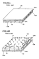
- Figs. 10A and 10B show an outline structure of the conventional BGA type semiconductor device.
- Fig. 10A is an oblique perspective figure showing a front side of the BGA type semiconductor device.
- Fig. 10B is an oblique perspective figure showing a back side of the BGA type semiconductor device.
- a semiconductor die 101 is sealed between a first glass substrate 104a and a second glass substrate 104b with resin 105a and 105b therebetween in the BGA type semiconductor device 100.
- a plurality of ball-shaped terminals (referred to as conductive terminals 111, hereafter) is arrayed in a grid pattern on one surface of the second glass substrate 104b, that is, on the back surface of the BGA type semiconductor device 100.
- the conductive terminals 111 are connected to the semiconductor die 101 through a plurality of second wirings 109.
- the plurality of second wirings 109 is connected with aluminum wirings pulled out from inside of the semiconductor die 101, making each of the conductive terminals 111 electrically connected with the semiconductor die 101.
- Fig. 11 shows a cross-sectional view of the BGA type semiconductor devices 100 separated into individual dies along borders (called scribe lines or dicing lines).
- a first wiring 103 is provided on an insulation film 102 on the front surface of the semiconductor die 101, as shown in Fig. 11.
- the semiconductor die 101 is attached to the first glass substrate 104a with the resin 105a.
- a back surface of the semiconductor die 101 is attached to the second glass substrate 104b with the resin 105b.
- One end of the first wiring 103 is connected to the second wiring 109.
- the second wiring 109 extends from the end of the first wiring 103 onto a surface of the second glass substrate 104b.
- the ball-shaped conductive terminal 111 is formed on the second wiring 109 extended onto the second glass substrate 104b.
- Figs. 12 to 14 are cross-sectional views showing a conventional BGA-type semiconductor device manufacturing method applicable to an image sensor chip.
- a first wiring 32 formed of an aluminum layer or an aluminum alloy layer is formed on a front surface of a semiconductor substrate 30 with a first insulation film 31 formed of a silicon oxide film, a silicon nitride film, or the like therebetween. Then, a glass substrate 34 is attached to the semiconductor substrate 30 including the first wiring 32 with an adhesive 33 formed of epoxy resin therebetween, for example.
- a resist film (not shown) is formed on the back surface of the semiconductor substrate 30, having an opening in a position corresponding to the first wiring 32. Then, dry-etching is performed to the semiconductor substrate 30 using the resist film as a mask, and further the insulation film 31 is etched to form an opening 35 from the back surface of the semiconductor substrate 30 to the first wiring 32.
- a second insulation film 36 is formed on the back surface of the semiconductor substrate 30 including in the opening 35, and the second insulation film 36 is etched to expose a front surface of the first wiring 32.
- a wiring layer 37 connected with the first wiring 32 is formed with the second insulation film 36 therebetween.
- a protection layer (not shown) is formed on the wiring layer 37, and an opening is provided in a predetermined position of the protection layer and a ball-shaped terminal 38 contacting the wiring layer 37 is formed.
- the semiconductor substrate and the layers layered thereon are then cut into individual semiconductor dies.
- the BGA-type semiconductor device where the first wiring 32 and the ball-shaped terminal 38 are electrically connected with each other is formed.
- the thickness of the second insulation film 36 becomes small as shown in Fig. 14, depending on the state of depositing the second insulation film 36 or the state of etching the second insulation film 36 in order to expose the front surface of the first wiring 32 after the deposition of the second insulation film 36, for example.
- This causes problems of reducing dielectric strength, or infiltrating treatment chemicals and the like into the semiconductor device from a silicon end portion through the opening 35 to corrode the first wiring 32.
- the thickness of the deposited insulation film on the bottom portion and sidewall portion of the opening 35 tends to be smaller than on the back surface of the semiconductor substrate 30 as shown in Fig. 14, so that the portion designated as A may be covered insufficiently. This can reduce resistance to moisture infiltration after manufacturing.
- the invention provides a semiconductor device that includes a semiconductor substrate having a hole penetrating through its thickness.
- the hole has a first end at the back surface of the substrate and a second end at the front surface of the substrate.
- the device also includes a first insulation film disposed on the front surface and having an opening overlapping with the hole of the substrate. This opening of the first insulation film is smaller than the second end of the hole.
- the device also includes a first wiring disposed on the first insulation film so as to cover the opening of the first insulation film, a second insulation film disposed on a sidewall of the hole of the substrate and the back surface of the substrate, and a second wiring disposed in the hole so as to be in contact with the first wiring, the first insulation film and the second insulation film.
- the invention also provides a method of manufacturing a semiconductor device.
- the method includes providing a semiconductor substrate having a first insulation film formed on its front surface and a first wiring formed on the first insulation film, etching the semiconductor substrate from its back surface to expose part of the first insulation film that corresponds to the first wiring, etching the exposed first insulation film to expose part of the first wiring, etching, after the exposure of the first wiring, the semiconductor substrate to expose an additional part of the first insulation film, forming a second insulation film to cover a sidewall of the semiconductor substrate that is formed by the etchings and to cover the back surface of the semiconductor substrate, and forming a second wiring that is on the second insulation film and is connected with the first wiring.
- the second insulation film lies at least on the first insulation film, thereby preventing problems of reduction of dielectric strength due to the insufficient covering for the insulation film as has been seen in the conventional art.
- The prevents the corrosion of the first wiring and the like caused by infiltration of chemicals and the like from the silicon end portion during the manufacturing process or infiltration of moisture and the like after the manufacturing process.
- Figs. 1 to 9 are cross-sectional views showing a method of manufacturing a BGA-type semiconductor device applicable to an image sensor chip.
- a semiconductor substrate 1 formed of a semiconductor wafer formed of, for example, silicon is prepared as shown in Fig. 1.
- This semiconductor substrate 1 has a device such as a CCD image sensor or a semiconductor memory formed by semiconductor processes.
- a first wiring 3 formed of aluminum, aluminum alloy, or copper is formed on a front surface of the semiconductor substrate 1 with a first insulation film 2 formed of, for example, a silicon oxide film or a silicon nitride film therebetween.
- the first wiring 3 is a pad electrode for external connection, being electrically connected with a circuit (not shown) of the semiconductor device.
- a passivation film formed of, for example, a silicon oxide film or a silicon nitride film covers the semiconductor substrate 1 including the first wiring 3.
- the adhesive 4 is not necessarily transparent and resist resin, acrylic resin, or the like can be used as the adhesive 4 regardless transparent or opaque unless the device is the image sensor.
- a first resist film 6 is formed on the back surface of the semiconductor substrate 1, having an opening in a position corresponding to the first wiring 3, and the semiconductor substrate 1 is dry-etched using the resist film 6 as a mask to form a first opening 7A exposing the first insulation film 2 from the back side of the semiconductor substrate 1, as shown in Fig. 2.
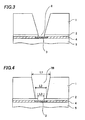
- the insulation film 2 exposed in the first opening 7A is etched to form a second opening 8 exposing a surface of the first wiring 3, as shown in Fig. 3. It is also possible to remove the resist film 6 after the second opening 8 is formed.
- the semiconductor substrate 1 is etched to increase a diameter of the first opening 7A and form a first opening 7B having the larger diameter, as shown in Fig. 4.
- an upper diameter L1 and a bottom diameter L2 of the first opening 7B are about 150 ⁇ m and 60 ⁇ m, respectively, and a diameter L3 of the second opening 8 is about 30 ⁇ m.
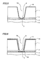
- a second insulation film 10 is formed on the back surface of the semiconductor substrate 1 including on the first wiring 3 through the first and second openings 7B and 8, as shown in Fig. 5.
- an inorganic insulation film is formed as the second insulation film 10.
- a TEOS film is formed by a low-temperature CVD (Chemical Vapor Deposition) method, for example.
- the inorganic insulation film has high covering properties and can achieve a stable covering form even in a three-dimensional structure.
- the insulation film formed in this process is not limited to the inorganic insulation film, and it is also possible to form an organic insulation film formed of, for example, epoxy resin.
- the organic insulation film is smooth in its surface, and thus effective for enhancing covering properties of a metal film (a second wiring 12 described below) to be deposited thereon.
- the second insulation film 10 covering the first wiring 3 is etched using the second resist film 11 formed on the back surface of the semiconductor substrate 1 as a mask to expose the first wiring 3.
- Fig. 9 shows a modification of this embodiment.
- This drawing shows a device intermediate corresponding to that of Fig. 6 of this embodiment.
- the inorganic insulation film 10a is first formed, the organic insulation film 10b is then formed, and these layered films are etched to expose the first wiring 14, as shown in Fig. 9.
- the described advantages of the inorganic insulation film and the organic insulation film can be provided, and this layered structure can enhance dielectric strength.
- the resist film 11 is used as a mask in this embodiment.
- the etching process can be performed by utilizing differences in thickness of the insulation films 10, 10a and 10b deposited on the bottom portion and the sidewall portion of the first and second openings 7B and 8 and on the back surface of the semiconductor substrate 1, without using the resist film as a mask. That is, the thicknesses of the insulation films 10, 10a and 10b are larger on the back surface of the semiconductor substrate 1 and reduces gradually toward the bottom portion of the hole.
- the insulation films 10, 10a and 10b deposited on the bottom portion are removed to expose the first wiring 3, the insulation films 10, 10a, and 10b deposited on the sidewall portion and on the back surface of the semiconductor substrate 1 still remain.
- the etching can be performed without a mask, and the process can be rationalized.
- the semiconductor substrate 1 and the first insulation film 2 are etched to form the first and second openings 7A and 8 exposing the first wiring 3, and then the semiconductor substrate 1 is etched to increase the diameter of the first opening 7A and form the first opening 7B having the larger diameter.
- the end portion of the second insulation films 10, 10a, and 10b after the second insulation films 10, 10a, and 10b formed in the first and second openings 7B and 8 are patterned forms a protrusion portion protruding in an inner direction of the first opening 7B from the end portion of the front surface of the semiconductor substrate 1.
- part of the second insulation film 10 is disposed on the first insulation film 2 that is exposed in the process step shown in Fig. 4 and extends toward the center of the opening 8.
- Fig. 6 shows this portion of the second insulation film 10 by referring to reference numeral 20.
- the second insulation film lies at least on the first insulation film 2 as shown in Fig. 6, thereby preventing problems of reduction of dielectric strength due to the insufficient covering for the insulation film as has been seen in the conventional art.
- The prevents the corrosion of the first wiring 3 and the like caused by infiltration of chemicals and the like from the silicon end portion during the manufacturing process or infiltration of moisture and the like after the manufacturing process.
- a second wiring 12 electrically connected with the first wiring 3 is formed in the first and second openings 7B and 8 with the second insulation film 10 therebetween as shown in Fig. 7.
- aluminum, aluminum alloy, or the like are deposited as the second wiring 12 by a sputtering method, for example.
- copper or the like is deposited by a plating method.
- a barrier film formed of a titanium nitride (TiN) film is formed under the second wiring 12.
- Metal having a high melting point such as a titanium (Ti) film or a tantalum (Ta) film, compounds of such metal such as a titanium tungsten (TiW) film, a tantalum nitride (TaN) film, or a layered film of these metal films can be deposited as the barrier film.
- a seed film for plating e.g. copper
- plating is performed on the seed film to form a wiring layer formed of copper.
- the wiring layer may be patterned or not be patterned.
- a protection film 13 is formed on the second wiring 12, openings are provided in a predetermined position of the protection film 13, and ball-shaped terminals 14 contacting the second wiring 12 are formed. It is possible that the second wiring 12 is formed only in the first and second openings 7B and 8 so as not to extend onto the back surface of the semiconductor substrate 1, and the second wiring 12 and the ball-shaped terminal 14 are connected in the first and second openings 7B and 8.
- the semiconductor substrate and the layers layered thereon are cut into individual semiconductor dies.
- the BGA-type semiconductor device where the first wiring 3 and the ball-shaped terminal 14 are electrically connected with each other is thus formed.
- this embodiment is described as applied to the semiconductor device formed with the ball-shaped terminal 14, the structure of the embodiment can be applied to the semiconductor device without the ball-shaped terminal as long as an opening penetrating the semiconductor substrate is formed, for example, to a LGA (Land Grid Array) type semiconductor device.
- LGA Land Grid Array
- a protection film 15 formed of an insulator covers the semiconductor substrate 1 including the first wiring 3.
- a protection film 15 in Fig. 8A completely covers the first wiring 3, it is possible that the protection film 15 covers only a part of the first wiring 3 to expose other of the first wiring 3.
Landscapes
- Internal Circuitry In Semiconductor Integrated Circuit Devices (AREA)
- Formation Of Insulating Films (AREA)
Abstract
Description
- The invention relates to a technology for enhancing a yield and reliability of a semiconductor device.
- CSP (Chip Size Package) has received attention in recent years as a packaging technology. The CSP means a small package having almost the same outside dimensions as those of a semiconductor die packaged in it. Conventionally, BGA (ball grid array) type semiconductor devices have been known as a kind of CSP. In this BGA type semiconductor device, a plurality of ball-shaped conductive terminals made of metal such as solder is arrayed in a grid pattern on one surface of the package, and electrically connected with the semiconductor die mounted on the other side of the package.
- When this BGA type semiconductor device is mounted on electronic equipment, the semiconductor die is electrically connected with an external circuit on a printed circuit board by compression bonding of the ball-shaped conductive terminals to wiring patterns on the printed circuit board.
- Such a BGA type semiconductor device has advantages in providing a large number of conductive terminals and in reducing size over other CSP type semiconductor devices such as SOP (Small Outline Package) and QFP (Quad Flat Package), which have lead pins protruding from their sides. The BGA type semiconductor device is used as an image sensor chip for a digital camera incorporated into a mobile telephone, for example.
- Figs. 10A and 10B show an outline structure of the conventional BGA type semiconductor device. Fig. 10A is an oblique perspective figure showing a front side of the BGA type semiconductor device. Fig. 10B is an oblique perspective figure showing a back side of the BGA type semiconductor device.
- A
semiconductor die 101 is sealed between afirst glass substrate 104a and asecond glass substrate 104b withresin type semiconductor device 100. A plurality of ball-shaped terminals (referred to asconductive terminals 111, hereafter) is arrayed in a grid pattern on one surface of thesecond glass substrate 104b, that is, on the back surface of the BGAtype semiconductor device 100. Theconductive terminals 111 are connected to the semiconductor die 101 through a plurality ofsecond wirings 109. The plurality ofsecond wirings 109 is connected with aluminum wirings pulled out from inside of thesemiconductor die 101, making each of theconductive terminals 111 electrically connected with thesemiconductor die 101. - More detailed explanation on the cross-sectional structure of the BGA
type semiconductor device 100 will be given hereafter referring to Fig. 11. Fig. 11 shows a cross-sectional view of the BGAtype semiconductor devices 100 separated into individual dies along borders (called scribe lines or dicing lines). - A
first wiring 103 is provided on aninsulation film 102 on the front surface of thesemiconductor die 101, as shown in Fig. 11. Thesemiconductor die 101 is attached to thefirst glass substrate 104a with theresin 105a. A back surface of thesemiconductor die 101 is attached to thesecond glass substrate 104b with theresin 105b. One end of thefirst wiring 103 is connected to thesecond wiring 109. Thesecond wiring 109 extends from the end of thefirst wiring 103 onto a surface of thesecond glass substrate 104b. The ball-shapedconductive terminal 111 is formed on thesecond wiring 109 extended onto thesecond glass substrate 104b. The technology mentioned above is disclosed in the Japanese Patent Application Publication No. 2002-512436. - A technology of not using the second glass substrate on the back surface of the semiconductor wafer is disclosed in the Japanese Patent Application Publication No. 2004-80006 by the inventors of this invention.
- Explanation on a BGA-type semiconductor device manufacturing method will be given particularly for a case that a sheet of supporting body is attached to a semiconductor die, with reference to figures.
- Figs. 12 to 14 are cross-sectional views showing a conventional BGA-type semiconductor device manufacturing method applicable to an image sensor chip.
- First, as shown in Fig. 12, a
first wiring 32 formed of an aluminum layer or an aluminum alloy layer is formed on a front surface of asemiconductor substrate 30 with afirst insulation film 31 formed of a silicon oxide film, a silicon nitride film, or the like therebetween. Then, aglass substrate 34 is attached to thesemiconductor substrate 30 including thefirst wiring 32 with an adhesive 33 formed of epoxy resin therebetween, for example. - Next, as shown in Fig. 13, a resist film (not shown) is formed on the back surface of the
semiconductor substrate 30, having an opening in a position corresponding to thefirst wiring 32. Then, dry-etching is performed to thesemiconductor substrate 30 using the resist film as a mask, and further theinsulation film 31 is etched to form anopening 35 from the back surface of thesemiconductor substrate 30 to thefirst wiring 32. - Then, a
second insulation film 36 is formed on the back surface of thesemiconductor substrate 30 including in theopening 35, and thesecond insulation film 36 is etched to expose a front surface of thefirst wiring 32. Then, as shown in Fig. 14, awiring layer 37 connected with thefirst wiring 32 is formed with thesecond insulation film 36 therebetween. Furthermore, a protection layer (not shown) is formed on thewiring layer 37, and an opening is provided in a predetermined position of the protection layer and a ball-shaped terminal 38 contacting thewiring layer 37 is formed. - Although not shown, the semiconductor substrate and the layers layered thereon are then cut into individual semiconductor dies. Thus, the BGA-type semiconductor device where the
first wiring 32 and the ball-shaped terminal 38 are electrically connected with each other is formed. - However, during the described manufacturing process of the semiconductor device, the thickness of the
second insulation film 36 becomes small as shown in Fig. 14, depending on the state of depositing thesecond insulation film 36 or the state of etching thesecond insulation film 36 in order to expose the front surface of thefirst wiring 32 after the deposition of thesecond insulation film 36, for example. This causes problems of reducing dielectric strength, or infiltrating treatment chemicals and the like into the semiconductor device from a silicon end portion through theopening 35 to corrode thefirst wiring 32. Particularly, the thickness of the deposited insulation film on the bottom portion and sidewall portion of the opening 35 tends to be smaller than on the back surface of thesemiconductor substrate 30 as shown in Fig. 14, so that the portion designated as A may be covered insufficiently. This can reduce resistance to moisture infiltration after manufacturing. - It is an object of this invention to provide a semiconductor device and manufacturing method thereof that lessens this drawback.
- The solution according to the invention lies in the features of the independent claims and preferably in those of the dependent claims.
- The invention provides a semiconductor device that includes a semiconductor substrate having a hole penetrating through its thickness. The hole has a first end at the back surface of the substrate and a second end at the front surface of the substrate. The device also includes a first insulation film disposed on the front surface and having an opening overlapping with the hole of the substrate. This opening of the first insulation film is smaller than the second end of the hole. The device also includes a first wiring disposed on the first insulation film so as to cover the opening of the first insulation film, a second insulation film disposed on a sidewall of the hole of the substrate and the back surface of the substrate, and a second wiring disposed in the hole so as to be in contact with the first wiring, the first insulation film and the second insulation film.
- The invention also provides a method of manufacturing a semiconductor device. The method includes providing a semiconductor substrate having a first insulation film formed on its front surface and a first wiring formed on the first insulation film, etching the semiconductor substrate from its back surface to expose part of the first insulation film that corresponds to the first wiring, etching the exposed first insulation film to expose part of the first wiring, etching, after the exposure of the first wiring, the semiconductor substrate to expose an additional part of the first insulation film, forming a second insulation film to cover a sidewall of the semiconductor substrate that is formed by the etchings and to cover the back surface of the semiconductor substrate, and forming a second wiring that is on the second insulation film and is connected with the first wiring.
- By virtue of the invention, the second insulation film lies at least on the first insulation film, thereby preventing problems of reduction of dielectric strength due to the insufficient covering for the insulation film as has been seen in the conventional art. The prevents the corrosion of the first wiring and the like caused by infiltration of chemicals and the like from the silicon end portion during the manufacturing process or infiltration of moisture and the like after the manufacturing process.
-
- Figs. 1-8A are cross-sectional views showing a semiconductor device manufacturing method of an embodiment of the invention.
- Fig. 9 is a cross-sectional view showing a semiconductor device manufacturing method of another embodiment of the invention.
- Figs. 10A and 10B are oblique perspective figures of a conventional semiconductor device.
- Figs. 11 to 14 are cross-sectional views showing a conventional semiconductor device manufacturing method.
- A semiconductor device and its manufacturing method of the invention will be described with reference to Figs. 1 to 9.
- Figs. 1 to 9 are cross-sectional views showing a method of manufacturing a BGA-type semiconductor device applicable to an image sensor chip.
- First, a
semiconductor substrate 1 formed of a semiconductor wafer formed of, for example, silicon is prepared as shown in Fig. 1. Thissemiconductor substrate 1 has a device such as a CCD image sensor or a semiconductor memory formed by semiconductor processes. Afirst wiring 3 formed of aluminum, aluminum alloy, or copper is formed on a front surface of thesemiconductor substrate 1 with afirst insulation film 2 formed of, for example, a silicon oxide film or a silicon nitride film therebetween. Thefirst wiring 3 is a pad electrode for external connection, being electrically connected with a circuit (not shown) of the semiconductor device. A passivation film formed of, for example, a silicon oxide film or a silicon nitride film covers thesemiconductor substrate 1 including thefirst wiring 3. - Then, a supporting
body 5 formed of, for example, a glass substrate, ceramic, quartz, plastic, resin (e.g. resist or epoxy resin), or the like is attached to thesemiconductor substrate 1 including thefirst wiring 3 with atransparent adhesive 4 formed of epoxy resin or the like therebetween. The adhesive 4 is not necessarily transparent and resist resin, acrylic resin, or the like can be used as the adhesive 4 regardless transparent or opaque unless the device is the image sensor. - Next, a first resist
film 6 is formed on the back surface of thesemiconductor substrate 1, having an opening in a position corresponding to thefirst wiring 3, and thesemiconductor substrate 1 is dry-etched using the resistfilm 6 as a mask to form afirst opening 7A exposing thefirst insulation film 2 from the back side of thesemiconductor substrate 1, as shown in Fig. 2. - Then, after the resist
film 6 is removed, theinsulation film 2 exposed in thefirst opening 7A is etched to form asecond opening 8 exposing a surface of thefirst wiring 3, as shown in Fig. 3. It is also possible to remove the resistfilm 6 after thesecond opening 8 is formed. - Next, the
semiconductor substrate 1 is etched to increase a diameter of thefirst opening 7A and form afirst opening 7B having the larger diameter, as shown in Fig. 4. In this embodiment, an upper diameter L1 and a bottom diameter L2 of thefirst opening 7B are about 150 µm and 60 µm, respectively, and a diameter L3 of thesecond opening 8 is about 30 µm. - Next, a
second insulation film 10 is formed on the back surface of thesemiconductor substrate 1 including on thefirst wiring 3 through the first andsecond openings second insulation film 10. As this inorganic insulation film, a TEOS film is formed by a low-temperature CVD (Chemical Vapor Deposition) method, for example. Generally, the inorganic insulation film has high covering properties and can achieve a stable covering form even in a three-dimensional structure. The insulation film formed in this process is not limited to the inorganic insulation film, and it is also possible to form an organic insulation film formed of, for example, epoxy resin. Generally, the organic insulation film is smooth in its surface, and thus effective for enhancing covering properties of a metal film (asecond wiring 12 described below) to be deposited thereon. - Next, as shown in Fig. 6, the
second insulation film 10 covering thefirst wiring 3 is etched using the second resistfilm 11 formed on the back surface of thesemiconductor substrate 1 as a mask to expose thefirst wiring 3. - Fig. 9 shows a modification of this embodiment. This drawing shows a device intermediate corresponding to that of Fig. 6 of this embodiment. In this modification, the
inorganic insulation film 10a is first formed, theorganic insulation film 10b is then formed, and these layered films are etched to expose thefirst wiring 14, as shown in Fig. 9. By this process, the described advantages of the inorganic insulation film and the organic insulation film can be provided, and this layered structure can enhance dielectric strength. - In the process of etching the
second insulation film 10 or the combination of theinorganic insulation film 10a and theorganic insulation film 10b, the resistfilm 11 is used as a mask in this embodiment. However, the etching process can be performed by utilizing differences in thickness of theinsulation films second openings semiconductor substrate 1, without using the resist film as a mask. That is, the thicknesses of theinsulation films semiconductor substrate 1 and reduces gradually toward the bottom portion of the hole. Therefore, using this tendency, when theinsulation films first wiring 3, theinsulation films semiconductor substrate 1 still remain. Thus, the etching can be performed without a mask, and the process can be rationalized. - In the embodiment, the
semiconductor substrate 1 and thefirst insulation film 2 are etched to form the first andsecond openings first wiring 3, and then thesemiconductor substrate 1 is etched to increase the diameter of thefirst opening 7A and form thefirst opening 7B having the larger diameter. By these processes, the end portion of thesecond insulation films second insulation films second openings first opening 7B from the end portion of the front surface of thesemiconductor substrate 1. In other words, part of thesecond insulation film 10 is disposed on thefirst insulation film 2 that is exposed in the process step shown in Fig. 4 and extends toward the center of theopening 8. Fig. 6 shows this portion of thesecond insulation film 10 by referring toreference numeral 20. - Thus, the second insulation film lies at least on the
first insulation film 2 as shown in Fig. 6, thereby preventing problems of reduction of dielectric strength due to the insufficient covering for the insulation film as has been seen in the conventional art. The prevents the corrosion of thefirst wiring 3 and the like caused by infiltration of chemicals and the like from the silicon end portion during the manufacturing process or infiltration of moisture and the like after the manufacturing process. - Going back to the explanation of the process flow, after the resist
film 11 is removed, asecond wiring 12 electrically connected with thefirst wiring 3 is formed in the first andsecond openings second insulation film 10 therebetween as shown in Fig. 7. In this embodiment, aluminum, aluminum alloy, or the like are deposited as thesecond wiring 12 by a sputtering method, for example. Alternatively, copper or the like is deposited by a plating method. Furthermore, although omitted in the figure, a barrier film formed of a titanium nitride (TiN) film is formed under thesecond wiring 12. Metal having a high melting point (refractory metal) such as a titanium (Ti) film or a tantalum (Ta) film, compounds of such metal such as a titanium tungsten (TiW) film, a tantalum nitride (TaN) film, or a layered film of these metal films can be deposited as the barrier film. In the case of forming a plating film of copper, a seed film for plating (e.g. copper) is formed on the barrier film, and plating is performed on the seed film to form a wiring layer formed of copper. The wiring layer may be patterned or not be patterned. - Then, as shown in Fig. 8, a
protection film 13 is formed on thesecond wiring 12, openings are provided in a predetermined position of theprotection film 13, and ball-shapedterminals 14 contacting thesecond wiring 12 are formed. It is possible that thesecond wiring 12 is formed only in the first andsecond openings semiconductor substrate 1, and thesecond wiring 12 and the ball-shapedterminal 14 are connected in the first andsecond openings - Then, although omitted in the figure, the semiconductor substrate and the layers layered thereon are cut into individual semiconductor dies. The BGA-type semiconductor device where the
first wiring 3 and the ball-shapedterminal 14 are electrically connected with each other is thus formed. - Although this embodiment is described as applied to the semiconductor device formed with the ball-shaped
terminal 14, the structure of the embodiment can be applied to the semiconductor device without the ball-shaped terminal as long as an opening penetrating the semiconductor substrate is formed, for example, to a LGA (Land Grid Array) type semiconductor device. - Although the supporting
body 5 is attached to the front surface of thesemiconductor substrate 1 in the described embodiment, this embodiment may be modified to include a semiconductor device without the supportingbody 5 and a manufacturing method thereof as shown in Fig. 8A. In Fig. 8A, aprotection film 15 formed of an insulator (e.g. a passivation film or a film layered with a passivation film and resin such as polyimide) covers thesemiconductor substrate 1 including thefirst wiring 3. Although theprotection film 15 in Fig. 8A completely covers thefirst wiring 3, it is possible that theprotection film 15 covers only a part of thefirst wiring 3 to expose other of thefirst wiring 3. This enables wire-bonding or formation of a bump electrode on the exposedfirst wiring 3, or connection of thefirst wiring 3 to a conductive terminal of the other semiconductor device when the semiconductor device is to be layered on the other semiconductor device. Furthermore, it is also possible that the supportingbody 5 is not used in the semiconductor device and the manufacturing method thereof of the embodiment shown in Fig. 9.
Claims (15)
- A semiconductor device comprising:- a semiconductor substrate (1) having a hole (7B) penetrating through a thickness thereof, the hole (7B) having a first end at a back surface of the substrate and a second end at a front surface of the substrate;- a first insulation film (2) disposed on the front surface and having an opening (8) overlapping with the hole (7B) of the substrate, the opening (8) of the first insulation film (2) being smaller than the second end of the hole (7B);- a first wiring (3, 14) disposed on the first insulation film (2) so as to cover the opening (8) of the first insulation film (2);- a second insulation film (10) disposed on a sidewall of the hole (7B) of the substrate (1) and the back surface of the substrate (1); and- a second wiring (12) disposed in the hole (7B) so as to be in contact with the first wiring (3), the first insulation film (2) and the second insulation film (10).
- The semiconductor device of claim 1, wherein a diameter of the opening (8) of the first insulation film (2) is smaller than a diameter of the second end of the hole (7B) of the substrate (1).
- The semiconductor device of claim 1 or 2, further comprising a supporting body (5) attached to the front surface of the semiconductor substrate (1).
- The semiconductor device according to any of claims 1 to 3, wherein part of the second insulation film (10) is disposed along a portion of the first insulation film (2) toward the opening (8) of the first insulation film (2), said portion of the first insulation film (2) being within the second end of the hole of the substrate (1).
- The semiconductor device of claim 2, wherein the diameter of the second end of the hole (7B) of the substrate (1) is smaller than a diameter of the first end of the hole (7B) of the substrate (1).
- The semiconductor device of claim 1, wherein the second insulation film (10) comprises a layer of an inorganic material, a layer of an organic material or a combination of a layer of an inorganic material (10a) and a layer of an organic material (10b).
- The semiconductor device of claim 1, further comprising a ball-shaped terminal (14) disposed on the second wiring (12).
- A method of manufacturing a semiconductor device, comprising:- providing a semiconductor substrate (1) comprising a first insulation film (2) formed on a front surface thereof and a first wiring (3, 14) formed on the first insulation film (2);- etching the semiconductor substrate (1) from a back surface thereof to expose part of the first insulation film (2) that corresponds to the first wiring (3, 14);- etching the exposed first insulation film (2) to expose part of the first wiring (3, 14);- etching, after the exposure of the first wiring (3, 14), the semiconductor substrate (1) to expose an additional part of the first insulation film (2);- forming a second insulation film (10) to cover a sidewall of the semiconductor substrate (1) that is formed by the etchings and to cover the back surface of the semiconductor substrate (1); and- forming a second wiring (12) that is on the second insulation film (10) and is connected with the first wiring (3, 14).
- The method of claim 8, further comprising attaching a supporting body (5) to the front surface of the semiconductor substrate (1).
- The method of claim 8 or 9, wherein the forming of the second insulation film (10) comprises forming a layer of an inorganic material, a layer of an organic material or a combination of a layer of an inorganic material (10a) and a layer of an organic material (10b).
- The method according to any of claims 8 to 10, further comprising etching the second insulation film (10) to expose part of the first wiring using a resist film as a mask.
- The method according to any of claims 8 to 10, further comprising etching the second insulation film (10) to expose part of the first wiring without using an etching mask.
- The method according to any of claims 8 to 12, further comprising forming a ball-shaped terminal (14) on the second wiring (12).
- The method according to any of claims 8 to 13, further comprising separating the semiconductor substrate (1) into a plurality of semiconductor dies.
- The method according to any of claims 8 to 14, wherein the etchings of the semiconductor substrate (1) are performed so that a tapered hole (7B) that has a smaller opening at the front surface is formed in the semiconductor substrate.
Applications Claiming Priority (1)
| Application Number | Priority Date | Filing Date | Title |
|---|---|---|---|
| JP2005022525 | 2005-01-31 |
Publications (2)
| Publication Number | Publication Date |
|---|---|
| EP1686622A2 true EP1686622A2 (en) | 2006-08-02 |
| EP1686622A3 EP1686622A3 (en) | 2010-05-05 |
Family
ID=36035797
Family Applications (1)
| Application Number | Title | Priority Date | Filing Date |
|---|---|---|---|
| EP06001902A Withdrawn EP1686622A3 (en) | 2005-01-31 | 2006-01-31 | Semiconductor device and manufacturing method of the same |
Country Status (6)
| Country | Link |
|---|---|
| US (1) | US8035215B2 (en) |
| EP (1) | EP1686622A3 (en) |
| JP (1) | JP4775007B2 (en) |
| KR (1) | KR100659625B1 (en) |
| CN (1) | CN100524725C (en) |
| TW (1) | TWI313914B (en) |
Families Citing this family (17)
| Publication number | Priority date | Publication date | Assignee | Title |
|---|---|---|---|---|
| JP4694305B2 (en) * | 2005-08-16 | 2011-06-08 | ルネサスエレクトロニクス株式会社 | Manufacturing method of semiconductor wafer |
| US8212331B1 (en) * | 2006-10-02 | 2012-07-03 | Newport Fab, Llc | Method for fabricating a backside through-wafer via in a processed wafer and related structure |
| KR101460141B1 (en) * | 2007-03-05 | 2014-12-02 | 인벤사스 코포레이션 | Chips having rear contacts connected by through vias to front contacts |
| JP5010948B2 (en) * | 2007-03-06 | 2012-08-29 | オリンパス株式会社 | Semiconductor device |
| JP4380718B2 (en) | 2007-03-15 | 2009-12-09 | ソニー株式会社 | Manufacturing method of semiconductor device |
| JP4483896B2 (en) | 2007-05-16 | 2010-06-16 | ソニー株式会社 | Semiconductor device and manufacturing method thereof |
| JP5245135B2 (en) * | 2007-06-30 | 2013-07-24 | 株式会社ザイキューブ | Semiconductor device having through conductor and method for manufacturing the same |
| JP2010114201A (en) * | 2008-11-05 | 2010-05-20 | Oki Semiconductor Co Ltd | Method of manufacturing semiconductor device |
| JP5460069B2 (en) * | 2009-02-16 | 2014-04-02 | パナソニック株式会社 | Semiconductor substrate, semiconductor package, and semiconductor substrate manufacturing method |
| JP2010232400A (en) * | 2009-03-27 | 2010-10-14 | Panasonic Corp | Semiconductor substrate, semiconductor substrate manufacturing method, and semiconductor package |
| JP2012134526A (en) * | 2012-02-22 | 2012-07-12 | Renesas Electronics Corp | Semiconductor device |
| JP5874690B2 (en) * | 2012-09-05 | 2016-03-02 | 株式会社デンソー | Manufacturing method of semiconductor device |
| JP6160901B2 (en) * | 2013-02-08 | 2017-07-12 | ローム株式会社 | Semiconductor device and manufacturing method thereof |
| JP6309243B2 (en) * | 2013-10-30 | 2018-04-11 | ラピスセミコンダクタ株式会社 | Semiconductor device and manufacturing method thereof |
| JP5871038B2 (en) * | 2014-08-19 | 2016-03-01 | セイコーエプソン株式会社 | Semiconductor device and electronic device |
| CN104615982B (en) * | 2015-01-28 | 2017-10-13 | 江阴长电先进封装有限公司 | The encapsulating structure and its method for packing of a kind of fingerprint Identification sensor |
| JP6335132B2 (en) | 2015-03-13 | 2018-05-30 | 東芝メモリ株式会社 | Semiconductor device and method for manufacturing semiconductor device |
Citations (2)
| Publication number | Priority date | Publication date | Assignee | Title |
|---|---|---|---|---|
| JP2002512436A (en) | 1998-02-06 | 2002-04-23 | シェルケース リミティド | Integrated circuit device |
| JP2004080006A (en) | 2002-06-18 | 2004-03-11 | Sanyo Electric Co Ltd | Manufacturing method of semiconductor device |
Family Cites Families (16)
| Publication number | Priority date | Publication date | Assignee | Title |
|---|---|---|---|---|
| JPS5613394B2 (en) * | 1974-11-29 | 1981-03-27 | ||
| JPH08181088A (en) | 1994-12-26 | 1996-07-12 | Murata Mfg Co Ltd | Method of forming fine contact holes |
| US5910687A (en) * | 1997-01-24 | 1999-06-08 | Chipscale, Inc. | Wafer fabrication of die-bottom contacts for electronic devices |
| KR100243286B1 (en) * | 1997-03-05 | 2000-03-02 | 윤종용 | Method for manufacturing a semiconductor device |
| US6052287A (en) * | 1997-12-09 | 2000-04-18 | Sandia Corporation | Silicon ball grid array chip carrier |
| US6617681B1 (en) * | 1999-06-28 | 2003-09-09 | Intel Corporation | Interposer and method of making same |
| JP3879816B2 (en) * | 2000-06-02 | 2007-02-14 | セイコーエプソン株式会社 | SEMICONDUCTOR DEVICE AND ITS MANUFACTURING METHOD, LAMINATED SEMICONDUCTOR DEVICE, CIRCUIT BOARD AND ELECTRONIC DEVICE |
| KR100796756B1 (en) * | 2001-11-12 | 2008-01-22 | 삼성전자주식회사 | A contact portion of a semiconductor device, a method of manufacturing the same, and a thin film transistor array substrate for a display device including the same, and a method of manufacturing the same |
| US20030119308A1 (en) * | 2001-12-20 | 2003-06-26 | Geefay Frank S. | Sloped via contacts |
| TWI229890B (en) * | 2003-04-24 | 2005-03-21 | Sanyo Electric Co | Semiconductor device and method of manufacturing same |
| JP4334397B2 (en) * | 2003-04-24 | 2009-09-30 | 三洋電機株式会社 | Semiconductor device and manufacturing method thereof |
| JP2004327910A (en) * | 2003-04-28 | 2004-11-18 | Sharp Corp | Semiconductor device and method of manufacturing the same |
| JP3970210B2 (en) | 2003-06-24 | 2007-09-05 | 三洋電機株式会社 | Manufacturing method of semiconductor device |
| JP3970211B2 (en) | 2003-06-24 | 2007-09-05 | 三洋電機株式会社 | Semiconductor device and manufacturing method thereof |
| JP2005093486A (en) * | 2003-09-12 | 2005-04-07 | Seiko Epson Corp | Semiconductor device manufacturing method and semiconductor device |
| JP4365750B2 (en) * | 2004-08-20 | 2009-11-18 | ローム株式会社 | Semiconductor chip manufacturing method and semiconductor device manufacturing method |
-
2005
- 2005-12-12 TW TW094143796A patent/TWI313914B/en not_active IP Right Cessation
-
2006
- 2006-01-27 KR KR1020060008792A patent/KR100659625B1/en not_active Expired - Fee Related
- 2006-01-27 US US11/340,851 patent/US8035215B2/en active Active
- 2006-01-28 CN CNB2006100042029A patent/CN100524725C/en not_active Expired - Fee Related
- 2006-01-30 JP JP2006020520A patent/JP4775007B2/en not_active Expired - Fee Related
- 2006-01-31 EP EP06001902A patent/EP1686622A3/en not_active Withdrawn
Patent Citations (2)
| Publication number | Priority date | Publication date | Assignee | Title |
|---|---|---|---|---|
| JP2002512436A (en) | 1998-02-06 | 2002-04-23 | シェルケース リミティド | Integrated circuit device |
| JP2004080006A (en) | 2002-06-18 | 2004-03-11 | Sanyo Electric Co Ltd | Manufacturing method of semiconductor device |
Also Published As
| Publication number | Publication date |
|---|---|
| EP1686622A3 (en) | 2010-05-05 |
| US8035215B2 (en) | 2011-10-11 |
| TWI313914B (en) | 2009-08-21 |
| KR20060088047A (en) | 2006-08-03 |
| CN1828883A (en) | 2006-09-06 |
| JP2006237594A (en) | 2006-09-07 |
| US20060180933A1 (en) | 2006-08-17 |
| JP4775007B2 (en) | 2011-09-21 |
| KR100659625B1 (en) | 2006-12-20 |
| TW200627598A (en) | 2006-08-01 |
| CN100524725C (en) | 2009-08-05 |
Similar Documents
| Publication | Publication Date | Title |
|---|---|---|
| US9165898B2 (en) | Method of manufacturing semiconductor device with through hole | |
| US7732925B2 (en) | Semiconductor device and manufacturing method thereof | |
| US7339273B2 (en) | Semiconductor device with a via hole having a diameter at the surface larger than a width of a pad electrode | |
| US8101496B2 (en) | Method of manufacturing ball grid array type semiconductor device | |
| US7582971B2 (en) | Semiconductor device and manufacturing method of the same | |
| EP1564807B1 (en) | Semiconductor device and manufacturing method of the same | |
| US7759247B2 (en) | Manufacturing method of semiconductor device with a barrier layer and a metal layer | |
| US8035215B2 (en) | Semiconductor device and manufacturing method of the same | |
| US20060033168A1 (en) | Manufacturing method of semiconductor device | |
| EP1482553A2 (en) | Semiconductor device and manufacturing method thereof | |
| US7241679B2 (en) | Method of manufacturing semiconductor device | |
| US7557017B2 (en) | Method of manufacturing semiconductor device with two-step etching of layer | |
| JP4845986B2 (en) | Semiconductor device |
Legal Events
| Date | Code | Title | Description |
|---|---|---|---|
| PUAI | Public reference made under article 153(3) epc to a published international application that has entered the european phase |
Free format text: ORIGINAL CODE: 0009012 |
|
| AK | Designated contracting states |
Kind code of ref document: A2 Designated state(s): AT BE BG CH CY CZ DE DK EE ES FI FR GB GR HU IE IS IT LI LT LU LV MC NL PL PT RO SE SI SK TR |
|
| AX | Request for extension of the european patent |
Extension state: AL BA HR MK YU |
|
| PUAL | Search report despatched |
Free format text: ORIGINAL CODE: 0009013 |
|
| AK | Designated contracting states |
Kind code of ref document: A3 Designated state(s): AT BE BG CH CY CZ DE DK EE ES FI FR GB GR HU IE IS IT LI LT LU LV MC NL PL PT RO SE SI SK TR |
|
| AX | Request for extension of the european patent |
Extension state: AL BA HR MK YU |
|
| RIC1 | Information provided on ipc code assigned before grant |
Ipc: H01L 21/768 20060101ALI20100329BHEP Ipc: H01L 23/485 20060101ALI20100329BHEP Ipc: H01L 23/31 20060101AFI20060327BHEP |
|
| 17P | Request for examination filed |
Effective date: 20101105 |
|
| 17Q | First examination report despatched |
Effective date: 20101213 |
|
| AKX | Designation fees paid |
Designated state(s): DE FR GB |
|
| GRAP | Despatch of communication of intention to grant a patent |
Free format text: ORIGINAL CODE: EPIDOSNIGR1 |
|
| INTG | Intention to grant announced |
Effective date: 20130409 |
|
| INTG | Intention to grant announced |
Effective date: 20130416 |
|
| GRAP | Despatch of communication of intention to grant a patent |
Free format text: ORIGINAL CODE: EPIDOSNIGR1 |
|
| INTG | Intention to grant announced |
Effective date: 20130821 |
|
| STAA | Information on the status of an ep patent application or granted ep patent |
Free format text: STATUS: THE APPLICATION IS DEEMED TO BE WITHDRAWN |
|
| 18D | Application deemed to be withdrawn |
Effective date: 20140103 |