EP1684430A1 - Buffer circuit and integrated circuit - Google Patents
Buffer circuit and integrated circuit Download PDFInfo
- Publication number
- EP1684430A1 EP1684430A1 EP05009107A EP05009107A EP1684430A1 EP 1684430 A1 EP1684430 A1 EP 1684430A1 EP 05009107 A EP05009107 A EP 05009107A EP 05009107 A EP05009107 A EP 05009107A EP 1684430 A1 EP1684430 A1 EP 1684430A1
- Authority
- EP
- European Patent Office
- Prior art keywords
- fet
- power source
- voltage
- circuit
- source
- Prior art date
- Legal status (The legal status is an assumption and is not a legal conclusion. Google has not performed a legal analysis and makes no representation as to the accuracy of the status listed.)
- Withdrawn
Links
Images






Classifications
-
- H—ELECTRICITY
- H03—ELECTRONIC CIRCUITRY
- H03K—PULSE TECHNIQUE
- H03K19/00—Logic circuits, i.e. having at least two inputs acting on one output; Inverting circuits
- H03K19/02—Logic circuits, i.e. having at least two inputs acting on one output; Inverting circuits using specified components
- H03K19/08—Logic circuits, i.e. having at least two inputs acting on one output; Inverting circuits using specified components using semiconductor devices
- H03K19/094—Logic circuits, i.e. having at least two inputs acting on one output; Inverting circuits using specified components using semiconductor devices using field-effect transistors
- H03K19/0944—Logic circuits, i.e. having at least two inputs acting on one output; Inverting circuits using specified components using semiconductor devices using field-effect transistors using MOSFET or insulated gate field-effect transistors, i.e. IGFET
- H03K19/0948—Logic circuits, i.e. having at least two inputs acting on one output; Inverting circuits using specified components using semiconductor devices using field-effect transistors using MOSFET or insulated gate field-effect transistors, i.e. IGFET using CMOS or complementary insulated gate field-effect transistors
-
- H—ELECTRICITY
- H03—ELECTRONIC CIRCUITRY
- H03K—PULSE TECHNIQUE
- H03K19/00—Logic circuits, i.e. having at least two inputs acting on one output; Inverting circuits
- H03K19/0008—Arrangements for reducing power consumption
- H03K19/0013—Arrangements for reducing power consumption in field effect transistor circuits
-
- H—ELECTRICITY
- H03—ELECTRONIC CIRCUITRY
- H03K—PULSE TECHNIQUE
- H03K17/00—Electronic switching or gating, i.e. not by contact-making and –breaking
- H03K17/22—Modifications for ensuring a predetermined initial state when the supply voltage has been applied
-
- H—ELECTRICITY
- H03—ELECTRONIC CIRCUITRY
- H03K—PULSE TECHNIQUE
- H03K17/00—Electronic switching or gating, i.e. not by contact-making and –breaking
- H03K17/22—Modifications for ensuring a predetermined initial state when the supply voltage has been applied
- H03K17/223—Modifications for ensuring a predetermined initial state when the supply voltage has been applied in field-effect transistor switches
-
- H—ELECTRICITY
- H03—ELECTRONIC CIRCUITRY
- H03K—PULSE TECHNIQUE
- H03K19/00—Logic circuits, i.e. having at least two inputs acting on one output; Inverting circuits
- H03K19/0175—Coupling arrangements; Interface arrangements
Definitions
- the present invention relates to a buffer circuit equipped with power sources having different voltages and including CMOS inverter circuits as logical gate circuits, or to an integrated circuit equipped with such a buffer circuit.
- Such an integrated circuit is configured to use power sources having voltages different depending on the function of the integrated circuit to lower the power voltages to the utmost extent and to reduce power consumption.
- the integrated circuit is equipped with a buffer circuit for signal interface between circuits that uses power sources having different voltages.
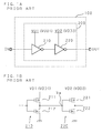
- FIG. 1A is a circuit diagram showing the configuration of a conventional buffer circuit (designated by numeral 200).
- a conventional buffer circuit designated by numeral 200.
- an output signal from a functional block (not shown), operating on a drive voltage VDD1 is inputted to the buffer circuit 200.
- the buffer circuit 200 outputs an output signal to another functional block (not shown) operating on a drive voltage VDD2 lower than VDD1.
- the buffer circuit 200 has a voltage step-down circuit for stepping down the drive voltage of the integrated circuit 100 from the high voltage VDD1 to the low voltage VDD2.
- the output of an inverter circuit 210 connected to a power source VD1 having the high voltage VDD1 is connected to the input of an inverter circuit 220 connected to a power source VD2 having the low voltage VDD2.
- FIG. 1B is a circuit diagram showing the specific circuit configurations of the two inverter circuits 210 and 220 shown in FIG. 1A.
- the inverter circuit 210 is composed of a P-channel FET 211 whose source is connected to the power source VD1, and an N-channel FET 212 whose source is connected to a drain of the FET 211. A drain of the FET 212 is grounded. Gates of the two FETs 211 and 212 are connected to each other and serve as the input terminal of the inverter circuit 210. Furthermore, a connection node of the drain of the FET 211 and the source of the FET 212 serves as the output terminal of the inverter circuit 210.
- the inverter circuit 220 is composed of a P-channel FET 221 whose source is connected to the power source VD2, and an N-channel FET 222 whose source is connected to a drain of the FET 221.
- the drain of the FET 222 is grounded.
- Gates of the two FETs 221 and 222 are connected to each other and serves as the input terminal of the inverter circuit 220.
- a connection node of the drain of the FET 221 and the source of the FET 222 serves as the output terminal of the inverter circuit 220.
- the power sources VD1 and VD2 are repeatedly turned ON and OFF depending on the operation state of the integrated circuit 100, for example, in the case that the power source VD1 is turned OFF to stop the operation of the functional block operating on the power source VD 1 or in the case that the power source VD2 is turned OFF to stop the operation of the functional block operating on the power source VD2. This reduces the power consumption of the circuit.
- Japanese Patent Application Laid-open No. 2000-341110 has proposed a CMOS transistor circuit in which an output of a first inverter circuit powered by a first power source is connected to an input of a second inverter circuit powered by a second power source, characterized in that an output of a third inverter circuit to which the first power source is inputted and which is powered by the second power source is connected to a gate of an N-channel FET, a drain of the N-channel FET is connected to the output of the first inverter circuit, and a source of the N-channel FET is grounded.
- this kind of conventional technology even in the case that the voltage of the first power source is lowered to the ground level, through current flows the second inverter circuit is prevented, whereby power consumption can be reduced.
- FIG. 2A, FIG. 2B and FIG. 2C are time charts showing operation states of the conventional buffer circuit 200 at the time of power-ON.
- FIG. 2A shows the changes in the voltages of the two power sources VD1 and VD2
- FIG. 2B shows the ON/OFF states of the two FETs 221 and 222 of the inverter circuit 220
- FIG. 2C shows the state of through current flowing the two FETs 221 and 222.
- the power source VD 1 is turned ON while the power source VD2 (voltage VDD2) is supplied to the buffer circuit 200 shown in FIG. 1, there is a period in which the voltage of the power source VD1 is lower than the voltage of the power source VD2.
- the FET 211 turns ON, whereby the voltage Va at the input terminal of the inverter circuit 220 becomes equal to the voltage of the power source VD1 and rises as the voltage of the power source VD1 rises.
- the voltage of the power source VD1 reaches a threshold voltage Vth of the FET 222, and the FET 222 turns ON.
- the voltage of the power source VD1 reaches a voltage obtained by subtracting the threshold voltage Vth of the FET 221 from the voltage VDD2, and the FET 221 turns OFF.
- the two FETs 221 and 222 are in the ON state in the period between time ta and time tb, whereby an unnecessary through current flows the two FETs 221 and 222, and the power consumption increases.
- FIG. 3A, FIG. 3B and FIG. 3C are time charts showing other operation states of the conventional buffer circuit 200 at the time of power-ON.
- FIG. 3A shows the changes in the voltages of the two power sources VD1 and VD2
- FIG. 3B shows the ON/OFF states of the two FETs 221 and 222 of the inverter circuit 220
- FIG. 3C shows the state of through current flowing the two FETs 221 and 222.
- the power source VD1 voltage VDD1
- the power source VD2 voltage VDD2
- the voltage of the power source VD 1 is lower than the voltage of the power source VD2.
- the FET 211 turns ON, whereby the voltage Va at the input terminal of the inverter circuit 220 becomes equal to the voltage of the power source VD1 and rises as the voltage of the power source VD1 rises.
- the voltage of the power source VD 1 reaches the threshold voltage Vth of the FET 222, and the FET 222 turns ON.
- the voltage of the power source VD1 reaches the voltage obtained by subtracting the threshold voltage Vth of the FET 221 from the voltage VDD2, and the FET 221 turns OFF.
- both the two FETs 221 and 222 are in the ON state in the period between time tc and time td, whereby an unnecessary through current flows the two FETs 221 and 222, and the power consumption increases.
- the second power source connected to the third inverter circuit is grounded via the third inverter circuit and the N-channel FET both being in the ON state, whereby an extra current may flow when the first power source is turned ON or OFF.
- a buffer circuit is a buffer circuit comprising: a first power source; a second power source different from the first power source; and a first logical gate circuit including CMOS inverter circuit and a second logical gate circuit; wherein the first logical gate circuit is powered by the first power source, and the second logical gate circuit is powered by the second power source and whose input terminal is connected to an output terminal of the first logical gate circuit; characterized by further comprising a power source switching circuit for switching the power source for the first logical gate circuit to the second power source when the voltage of the first power source is lower than the voltage of the second power source, and to the first power source when the voltage of the first power source is higher than the voltage of the second power source.
- a buffer circuit according to a second invention is a buffer circuit in accordance with the first invention, characterized in that the power source switching circuit comprises a first switching element for supplying the voltage of the first power source to the first logical gate circuit and a second switching element for supplying the voltage of the second power source to the first logical gate circuit, and turns ON or OFF the first switching element or the second switching element depending on high or low of the voltage of the first power source and the second power source.
- a buffer circuit according to a third invention is a buffer circuit in accordance with the second invention, characterized in that the CMOS inverter circuit including a first FET of a P-channel FET, and a second FET of an N-channel FET whose source and gate are connected to a drain and a gate of the first FET, respectively;
- the first switching element is a third FET of a P-channel FET whose source is connected to the first power source and whose gate is connected to the second power source;
- the second switching element is a fourth FET of a P-channel FET whose source is connected to the second power source, whose gate is connected to the first power source and whose drain is connected to a drain of the third FET; and the drain of the fourth switching element is connected to a source of the first FET of the first logical gate circuit.
- a buffer circuit according to a fourth invention is a buffer circuit in accordance with the second invention, characterized in that the CMOS inverter circuit including a first FET of a P-channel FET, and a second FET of an N-channel FET whose source and gate are connected to a drain and a gate of the first FET, respectively;
- the first switching element is a third FET of a P-channel FET whose source is connected to the first power source and whose gate is connected to the second power source;
- the second switching element is a fourth FET of a P-channel FET whose source is connected to the second power source and whose drain is connected to the source of the first FET of the first logical gate circuit and a drain of the third FET;
- the buffer circuit further comprising a fifth FET of a P-channel FET and a sixth FET of an N-channel FET whose respective sources are connected to each other and also connected to the first power source, whose respective drains are connected to each other and also connected to
- a buffer circuit according to a fifth invention is a buffer circuit in accordance with the third or fourth invention, characterized by further comprising a seventh FET of a P-channel FET whose source is connected to the respective drains of the third FET and the fourth FET and whose gate is connected to the second power source, wherein a drain and a back gate of the seventh FET are connected to back gates of the first, third, fourth and fifth FETs.
- a buffer circuit according to a sixth invention is a buffer circuit in accordance with the third or fourth invention, characterized by further comprising: a seventh FET of a P-channel FET whose source is connected to the respective drains of the third FET and the fourth FET; and an eighth FET of an N-channel FET whose gate and drain are connected to the second power source and whose source is connected to a gate of the seventh FET; wherein a drain and a back gate of the seventh FET are connected to back gates of the first, third, fourth and fifth FETs.
- An integrated circuit according to a seventh invention comprises a functional block powered by a first power source and a functional block powered by a second power source different from the first power source, characterized by further comprising the buffer circuit in accordance with any one of the first invention through the sixth invention.
- the power source switching circuit switches the power source for the first logical gate circuit to the second power source.
- the voltage at the input terminal of the first logical gate circuit including the CMOS inverter circuit is 0V
- the voltage at the output terminal of the first logical gate circuit becomes equal to the voltage of the second power source. Since the input terminal of the second logical gate circuit is connected to the output terminal of the first logical gate circuit, the voltage at the input terminal of the second logical gate circuit becomes equal to the voltage of the second power source. Hence, no through current is generated in the second logical gate circuit.
- the power source switching circuit switches the power source for the first logical gate circuit to the first power source.
- the voltage at the input terminal of the first logical gate circuit is 0V
- the voltage at the output terminal of the first logical gate circuit becomes equal to the voltage of the first power source. Since the input terminal of the second logical gate circuit is connected to the output terminal of the first logical gate circuit, the voltage at the input terminal of the second logical gate circuit becomes equal to the voltage of the first power source. Since the voltage of the first power source is higher than the voltage of the second power source, no through current is generated in the second logical gate circuit.
- the first switching element turns OFF, and the second switching element turns ON.
- the power source for the first logical gate circuit is switched to the second power source.
- the first switching element turns ON, and the second switching element turns OFF.
- the power source for the first logical gate circuit is switched to the first power source.
- the third FET turns OFF, and the fourth FET turns ON.
- the second power source becomes the power source for the first logical gate circuit via the source and drain of the fourth FET having been turned ON.
- the first FET of a P-channel FET turns ON, and the voltage at the output terminal of the first logical gate circuit becomes equal to the voltage of the second power source. Since the input terminal of the second logical gate circuit is connected to the output terminal of the first logical gate circuit, the voltage at the input terminal of the second logical gate circuit becomes equal to the voltage of the second power source.
- the gate voltage of the P-channel FET of the inverter circuit included in the second logical gate circuit becomes equal to the source voltage thereof, and the FET turns OFF, whereby no through current is generated in the second logical gate circuit.
- the third FET turns ON, and the fourth FET turns OFF.
- the first power source becomes the power source for the first logical gate circuit via the source and drain of the third FET having been turned ON.
- the first FET of a P-channel FET turns ON, and the voltage at the output terminal of the first logical gate circuit becomes equal to the voltage of the first power source. Since the input terminal of the second logical gate circuit is connected to the output terminal of the first logical gate circuit, the voltage at the input terminal of the second logical gate circuit becomes equal to the voltage of the first power source.
- the gate voltage of the P-channel FET of the inverter circuit included in the second logical gate circuit becomes higher than the source voltage thereof, and the FET turns OFF, whereby no through current is generated in the second logical gate circuit.
- the fifth FET of a P-channel FET whose gate is connected to the second power source and whose source is connected to the first power source turns OFF.
- the sixth FET of an N-channel FET whose gate is connected to the second power source and whose source is connected to the first power source is saturated in a range wherein the voltage of the first power source is higher than the voltage obtained by subtracting the threshold voltage of the sixth FET from the voltage of the second power source.
- the gate voltage of the fourth FET is the voltage obtained by subtracting the threshold voltage of the sixth FET from the voltage of the second power source. Since the voltage lower than the voltage of the second power source is applied to the gate, the ON operation of the fourth FET is speeded up.
- the fifth FET of a P-channel FET whose gate is connected to the second power source and whose source is connected to the first power source turns ON.
- the gate voltage of the fourth FET becomes equal to the voltage of the first power source.
- the third FET turns OFF, and the fourth FET turns ON. Since the gate voltage and the source voltage of the seventh FET become equal to the voltage of the second power source, the back gate voltages of the first, third, fourth, fifth and seventh FETs become almost equal to the voltage of the second power source by virtue of the PN forward bias from the source of the seventh FET.
- the third FET turns ON, and the fourth FET turns OFF.
- the gate voltage of the seventh FET becomes lower than the source voltage thereof, the seventh FET turns ON.
- the drain voltage of the seventh FET becomes equal to the voltage of the first power source. Since the drain of the seventh FET is connected to the back gates of the first, third, fourth, fifth and seventh FETs, the back gate voltages of the first, third, fourth, fifth and seventh FETs become equal to the voltage of the first power source.
- the fifth FET of a P-channel FET whose gate is connected to the second power source and whose source is connected to the first power source turns OFF.
- the sixth FET of an N-channel FET whose gate is connected to the second power source and whose source is connected to the first power source turns ON, the third FET turns OFF, and the fourth FET turns ON.
- the eighth FET whose gate and drain are connected to the second power source is saturated.
- the gate voltage of the seventh FET becomes the voltage obtained by subtracting the threshold voltage of the eighth FET from the voltage of the second power source. Since the voltage lower than the voltage of the second power source is applied to the gate of the seventh FET, the ON operation of the seventh FET is speeded up.
- the output signal of the functional block powered by the first power source is used as the input signal of the functional block powered by the second power source via such a buffer circuit as described above.
- the first, second and seventh invention comprise the power source switching circuit for switching the power source for the first logical gate circuit to either the first power source or the second power source in accordance with the voltages of the first and second power sources.
- the third invention comprises the third FET whose source is connected to the first power source and whose gate is connected to the second power source, and the fourth FET whose source is connected to the second power source and whose gate is connected to the first power source.
- the fourth invention comprises the third FET whose source is connected to the first power source and whose gate is connected to the second power source, the fourth FET whose source is connected to the second power source, and the fifth FET of a P-channel FET and the sixth FET of an N-channel FET whose sources, drains and gates are respectively connected to each other. Hence, the ON operation of the fourth FET can be speeded up.
- the fifth invention comprises the seventh FET whose gate is connected to the second power source and whose source is connected to the respective drains of the third FET and the fourth FET. Hence, even in the case that switching is carried out between the first power source and the second power source, the back gate voltages of the first, third, fourth, fifth and seventh FETs can be stabilized.
- the sixth invention comprises the eighth FET of an N-channel FET whose gate and drain are connected to the second power source, and the seventh FET whose gate is connected to the source of the eighth FET. Hence, the ON operation of the seventh FET can be speeded up.
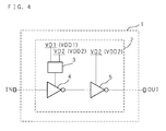
- FIG. 4 is a block diagram showing the configuration of a buffer circuit (designated by numeral 2) according to the present invention.
- An output signal from a functional block (not shown), operating on a drive voltage VDD1, for attaining a predetermined function inside an integrated circuit 1 is inputted to the buffer circuit 2.
- the buffer circuit 2 outputs an output signal to another functional block (not shown) operating on a drive voltage VDD2 lower than VDD1.
- the buffer circuit 2 steps down the drive voltage of the integrated circuit 1 from the high voltage VDD1 to the low voltage VDD2.
- the buffer circuit 2 has CMOS inverter circuits 4 and 5 as logical gate circuits and a power source switching circuit 3.
- a power source VD1 having the voltage VDD1 and a power source VD2 having the voltage VDD2 lower than the voltage VDD1 are connected to the power source switching circuit 3.
- the power source switching circuit 3 carries out switching so that either the power source VD1 or the power source VD2 is connected to the inverter circuit 4.
- An output of the inverter circuit 4 is connected to an input of the inverter circuit 5.
- the power source VD2 is connected to the inverter circuit 5.
- FIG. 5 is a circuit diagram showing the specific circuit configurations of the inverter circuits 4 and 5 and the power source switching circuit 3 constituting the buffer circuit 2.
- the inverter circuit 4 is composed of a P-channel FET 41 and an N-channel FET 42. Gates of the two FETs 41 and 42 are connected to each other, and the connection node thereof serves as an input terminal of the inverter circuit 4. A drain of the FET 41 is connected to a source of the FET 42, and a connection node thereof serves as an output terminal of the inverter circuit 4. A drain of the FET 42 is grounded. A source of the FET 41 is connected to the power source switching circuit 3.
- the power source switching circuit 3 is composed of P-channel FETs 31, 32 and 33.
- a source and a gate of the FET 31 are connected to the power source VD1 and the power source VD2, respectively.
- a drain of the FET 31 is connected to the source of the FET 41.
- a source and a gate of the FET 32 are connected to the power source VD2 and the power source VD1, respectively.
- a drain of the FET 32 is connected to a source of the FET 33.
- a gate of the FET 33 is connected to the power source VD2.
- a drain of the FET 33 is connected to back gates of the FETs 31, 32, 33 and 41.
- the connection node of the drain of the FET 31 and a source of the FET 41 is connected to a connection node of the drain of the FET 32 and the source of the FET 33.
- the output terminal of the inverter circuit 4 is connected to an input terminal of the inverter circuit 5.
- the inverter circuit 5 is composed of a P-channel FET 51 and an N-channel FET 52. Gates of the FETs 51 and 52 are connected to each other, and the connection node thereof serves as the input terminal of the inverter circuit 5.
- a source of the FET 51 is connected to the power source VD2.
- a drain of the FET 51 is connected to a source of the FET 52, and the connection node thereof serves as an output terminal of the inverter circuit 5.
- a drain of the FET 52 is grounded.
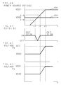
- FIG. 6A, FIG. 6B, FIG. 6C and FIG. 6D are time charts showing operation states of the buffer circuit 2 at the time of power-ON.
- FIG. 6A shows the changes in the voltages of the two power sources VD1 and VD2
- FIG. 6B shows the ON/OFF states of the two FETs 31 and 32 of the power source switching circuit 3
- FIG. 6C shows the state at the connection node of the power source switching circuit 3 and the inverter circuit 4, more specifically, the state of the voltage Vb at the connection node of the drain of the FET 31 of the power source switching circuit 3 and the source of the FET 41 of the inverter circuit 4
- FIG. 6D shows the state of the voltage Va at the input terminal of the inverter circuit 5.
- the FET 41 when the voltage at the input terminal of the inverter circuit 4 is 0V, the FET 41 is in the ON state, and the voltage at the output terminal of the inverter circuit 4 becomes equal to the voltage VDD2 of the power source VD2. Hence, the voltage Va at the input terminal of the inverter circuit 5 also becomes equal to the voltage VDD2 as shown in FIG. 6D.
- the FET 32 When the voltage of the power source VD1 rises with the passage of time and reaches a voltage lower than the voltage VDD2 of the power source VD2 by the threshold voltage Vth of the FET 32 at time t1 as shown in FIG. 6A, the FET 32 turns from ON to OFF as shown in FIG. 6B. Furthermore, when the voltage of the power source VD 1 reaches a voltage higher than the voltage VDD2 of the power source VD2 by the threshold voltage Vth of the FET 31 at time t2, the FET 31 turns from OFF to ON as shown in FIG. 6B. Since the FET 31 turns ON at this time, the voltage of the power source VD1 is applied to the source of the FET 41 via the source and drain of the FET 31.
- the voltage Vb at the source of the FET 41 rises gradually and reaches the voltage VDD1 at time t3 as shown in FIG. 6C. It is assumed that the voltage Vb at time t2 when the FET 31 turns from OFF to ON is VDD2 for the sake of simplicity.
- the voltage Va at the input terminal of the inverter circuit 5 changes in a manner similar to the voltage Vb at the source of the FET 41 by virtue of the above-mentioned operation as shown in FIG. 6D.
- the gate voltage of the FET 51 of the inverter circuit 5 can be prevented from becoming lower than the source voltage (VDD2).
- the FET 51 does not turn ON, it is thus possible to suppress the generation of through current flowing the FETs 51 and 52.
- the power source VD2 is connected to the inverter circuit 4 by the power source switching circuit 3.
- the inverter circuit 4 can output a signal to the inverter circuit 5 in accordance with a signal inputted to the inverter circuit 4 itself.
- the source voltage Vb of the FET 41 becomes equal to the voltage of the power source VD2.
- the voltage at the source of the FET 33 connected to the source of the FET 41 also becomes equal to the voltage of the power source VD2.
- the gate of the FET 33 since the gate of the FET 33 is connected to the power source VD2, the gate voltage and the source voltage of the FET 33 become equal, and the FET 33 turns OFF.
- the drain of the FET 33 is connected to the back gates of the FETs 31, 32, 33 and 41, the back gate voltages of the FETs 31, 32, 33 and 41 become almost equal to the voltage of the power source VD2 by virtue of the PN forward bias from the source of the FET 33, whereby the circuit can be operated stably.
- the source voltage Vb of the FET 41 becomes equal to the voltage of the power source VD1
- the source voltage of the FET 33 connected to the source of the FET 41 also becomes equal to the voltage of the power source VD 1.
- the gate of the FET 33 since the gate of the FET 33 is connected to the power source VD2, the FET 33 turns ON. Since the drain of the FET 33 is connected to the back gates of the FETs 31, 32, 33 and 41, the back gate voltages of the FETs 31, 32, 33 and 41 become equal to the voltage of the power source VD1, whereby the circuit can be operated stably.
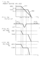
- FIG. 7A, FIG. 7B, FIG. 7C and FIG. 7D are time charts showing operation states of the buffer circuit 2 at the time of power-OFF.
- FIG. 7A shows the changes in the voltages of the two power sources VD1 and VD2
- FIG. 7B shows the ON/OFF states of the FETs 31 and 32 of the power source switching circuit 3
- FIG. 7C shows the state at the connection node of the power source switching circuit 3 and the inverter circuit 4, more specifically, the state of the voltage Vb at the connection node of the drain of the FET 31 of the power source switching circuit 3 and the source of the FET 41 of the inverter circuit 4
- FIG. 7D shows the state of the voltage Va at the input terminal of the inverter circuit 5.
- the power source VD1 is turned OFF while the power source VD2 (voltage VDD2) is supplied to the buffer circuit 2
- the lowering of the voltage of the power source VD1 takes time, therefore there is a transient period in which the voltage of the power source VD1 is higher than the voltage of the power source VD2.
- the voltage of the power source VD1 eventually becomes lower than the voltage of the power source VD2.
- the FET 32 turns ON and the FET 31 turns OFF.
- the source voltage Vb of the FET 41 becomes equal to the voltage VDD2 of the power source VD2.
- the FET 41 when the voltage at the input terminal of the inverter circuit 4 is 0V, the FET 41 is in the ON state. Hence, the voltage at the output terminal of the inverter circuit 4 becomes equal to the voltage VDD2 of the power source VD2, and the voltage Va at the input terminal of the inverter circuit 5 also becomes equal to the voltage VDD2.
- the FET 31 turns from ON to OFF as shown in FIG. 7B. Furthermore, when the voltage of the power source VD1 reaches the voltage lower than the voltage VDD2 of the power source VD2 by the threshold voltage Vth of the FET 32 at time t6, the FET 32 turns from OFF to ON.
- the FET 32 Since the FET 32 turns ON, the voltage of the power source VD2 is applied to the source of the FET 41 via the source and drain of the FET 32. Hence, the source voltage Vb of the FET 41 is fixed at the voltage of the power source VD2 as shown in FIG. 7C.
- the voltage Va at the input terminal of the inverter circuit 5 changes in a manner similar to the source voltage Vb of the FET 41 as shown in FIG. 7D.
- the gate voltage of the FET 51 of the inverter circuit 5 can be prevented from becoming lower than the source voltage (VDD2).
- the FET 51 does not turn ON, and it is thus possible to suppress the generation of thorough current flowing the FETs 51 and 52.
- FIG. 8A, FIG. 8B, FIG. 8C and FIG. 8D are time charts showing other operation states of the buffer circuit 2 at the time of power-ON.
- FIG. 8A shows the changes in the voltages of the two power sources VD1 and VD2
- FIG. 8B shows the ON/OFF states of the FETs 31 and 32 of the power source switching circuit 3
- FIG. 8C shows the state at the connection node of the power source switching circuit 3 and the inverter circuit 4, more specifically, the state of the voltage Vb at the connection node of the drain of the FET 31 of the power source switching circuit 3 and the source of the FET 41 of the inverter circuit 4
- FIG. 8D shows the state of the voltage Va at the input terminal of the inverter circuit 5.
- the FET 41 when the voltage at the input terminal of the inverter circuit 4 is 0V, the FET 41 is in the ON state. Hence, the voltage at the output terminal of the inverter circuit 4 becomes equal to the voltage VDD2 of the power source VD2, and the voltage Va at the input terminal of the inverter circuit 5 also becomes equal to the voltage VDD2.
- the FET 31 turns from OFF to ON as shown in FIG. 8B. Since the FET 31 turns ON, the voltage of the power source VD1 is applied to the source of the FET 41 via the source and drain of the FET 31. Hence, the source voltage Vb of the FET 41 rises depending on the voltage of the power source VD1 and reaches the voltage VDD1 at time t15 as shown in FIG. 8C.
- the voltage Va at the input terminal of the inverter circuit 5 changes in a manner similar to the voltage Vb at the source of the FET 41 as shown in FIG. 8D.
- the gate voltage of the FET 51 of the inverter circuit 5 can be prevented from becoming lower than the source voltage (VDD2).
- the FET 51 does not turn ON, and it is thus possible to suppress the generation of through current flowing the FETs 51 and 52.
- FIG. 9A, FIG. 9B, FIG. 9C and FIG. 9D are time charts showing other operation states of the buffer circuit 2 at the time of power-OFF.
- FIG. 9A shows the changes in the voltages of the two power sources VD1 and VD2
- FIG. 9B shows the ON/OFF states of the FETs 31 and 32 of the power source switching circuit 3
- FIG. 9C shows the state at the connection node of the power source switching circuit 3 and the inverter circuit 4, more specifically, the state of the voltage Vb at the connection node of the drain of the FET 31 of the power source switching circuit 3 and the source of the FET 41 of the inverter circuit 4
- FIG. 9D shows the state of the voltage Va at the input terminal of the inverter circuit 5.
- the voltage of the power source VD1 begins to lower earlier.
- the voltage of the power source VD1 is lower than the voltage of the power source VD2.
- both the voltage of the power source VD1 and the voltage of the power source VD2 become OV eventually.
- the FET 32 turns ON and the FET 31 turns OFF.
- the source voltage Vb of the FET 41 becomes equal to the voltage VDD2 of the power source VD2.
- the FET 41 when the voltage at the input terminal of the inverter circuit 4 is 0V, the FET 41 is in the ON state. Hence, the voltage at the output terminal of the inverter circuit 4 becomes equal to the voltage VDD2 of the power source VD2, and the voltage Va at the input terminal of the inverter circuit 5 also becomes equal to the voltage VDD2.
- the FET 31 turns from ON to OFF as shown in FIG. 9B. Furthermore, when the voltage of the power source VD1 reaches the voltage lower than the voltage VDD2 of the power source VD2 by the threshold voltage Vth of the FET 32 at time t18 as shown in FIG. 9A, the FET 32 turns from OFF to ON as shown in FIG. 9B.
- the FET 32 Since the FET 32 turns ON, the voltage of the power source VD2 is applied to the source of the FET 41 via the source and drain of the FET 32. Hence, the source voltage Vb of the FET 41 changes depending on the voltage of the power source VD2 as shown in FIG. 9C.
- the voltage Va at the input terminal of the inverter circuit 5 changes in a manner similar to the voltage Vb at the source of the FET 41 as shown in FIG. 9D.
- the gate voltage of the FET 51 of the inverter circuit 5 can be prevented from becoming lower than the source voltage (VDD2).
- the FET 51 does not turn ON, and it is thus possible to suppress the generation of through current flowing the FETs 51 and 52.
- the buffer circuit 2 equipped with the power sources (VD1 and VD2) having different voltages in the case that the power sources VD1 and VD2 are turned ON or OFF, switching is carried out between the power sources VD1 and VD2 depending on the high or low of the voltage between the power source VD1 and the power source VD2, whereby the voltage at the input terminal of the inverter circuit 5 is prevented from becoming lower than the voltage of the power source VD2.
- the inverter circuit 5 is prevented, whereby the power consumption of the buffer circuit can be made lower than that of this kind of conventional circuit.
- the power source VD1 is turned OFF
- the voltage of the power source VD2 is applied to the first logical gate circuit, whereby the function of the inverter circuit 4 does not stop.
- a signal inputted to the inverter circuit 4 can be outputted to the inverter circuit 5, and signal transmission can thus be carried out inside the integrated circuit 1.
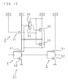
- FIG. 10 is a circuit diagram showing the specific circuit configuration of a buffer circuit according to Embodiment 2 of the present invention.
- a buffer circuit 21 according to Embodiment 2 is equipped with a transmission gate which is composed of a P-channel FET 34 and an N-channel FET 35 and is inserted between the power source VD 1 and the gate of the FET 32 of a power source switching circuit 3, in addition to the buffer circuit according to Embodiment 1.
- a source of the FET 34 is connected to a source of the FET 35 and also connected to the power source VD1.
- a gate of the FET 34 is connected to a gate of the FET 34 and also connected to the power source VD2 and the gate of the FET 33.
- a drain of the FET 34 is connected to a drain of the FET 35 and also connected to the gate of the FET 32.
- a back gate of the FET 34 is connected to the back gates of the FETs 31, 32, 33 and 41.
- Other components similar to those of Embodiment 1 are designated by the same numerals and their descriptions are omitted.
- the FET 35 constituting the transmission gate becomes saturation at about time t1 to time t2 shown in FIG. 6A, at about time t5 to time t6 shown in FIG. 7A, at about time t13 to time t14 shown in FIG. 8A and at about time t17 to time t18 shown in FIG. 9A.
- the gate voltage of the FET 32 becomes the voltage obtained by subtracting the threshold voltage of the FET 35 from the voltage of the power source VD2, and the voltage lower than the voltage of the power source VD2 is applied to the gate of the FET 32.
- time t1 in FIG. 6A and time t13 in FIG. 8A can be delayed, and time t6 in FIG. 7A and time t18 in FIG. 9A can be advanced.
- the FET 34 and the FET 31 carry out the same operation, for example, in the case that the voltage of the power source VD1 becomes higher than the voltage of the power source VD2, the FET 34 turns ON at the same time when the FET 31 turns ON. Hence, the gate voltage of the FET 32 becomes equal to the voltage of the power source VD 1, and the FET 32 turns OFF.
- the transmission gate which is composed of the FETs 34 and 35 is inserted between the power source VD1 and the gate of the FET 32, whereby the time required for power source switching can be shortened in comparison with the case wherein the voltage of the power source VD2 is applied to the gate of the FET 32.
- FIG. 11 is a circuit diagram showing the specific circuit configuration of a buffer circuit according to Embodiment 3 of the present invention.
- a buffer circuit 22 according to Embodiment 3 is equipped with an N-channel FET 36 connected between the power source VD2 and the gate of the FET 33 of a power source switching circuit 3, in addition to the buffer circuit according to Embodiment 2.
- a gate and a drain of the FET 36 are connected to the power source VD2.
- a source of the FET 36 is connected to the gate of the FET 33.
- Other components similar to those of Embodiment 2 are designated by the same numerals and their descriptions are omitted.
- the P-channel FET 34 turns OFF since its gate voltage becomes higher than its source voltage.
- the N-channel FET 35 turns ON since its gate voltage becomes higher than its source voltage.
- the FET 31 turns OFF since its gate voltage becomes higher than its source voltage.
- the FET 32 turns ON since its gate voltage becomes lower than its source voltage.
- the FET 36 Since the gate voltage and the source voltage of the FET 36 are equal to the voltage of the power source VD2, the FET 36 becomes saturation. Hence, the gate voltage of the FET 33 becomes the voltage obtained by subtracting the threshold voltage of the FET 36 from the voltage of the power source VD2, and the voltage lower than the voltage of the power source VD2 is applied to the gate of the FET 33. As a result, in comparison with the case wherein the voltage of the power source VD2 is applied to the gate of the FET 33, the ON operation of the FET 33 can be hastened.
- the source voltage Vb of the FET 41 becomes equal to the voltage of the power source VD1.
- the source voltage of the FET 33 connected to the source of the FET 41 also becomes equal to the voltage of the power source VD1.
- the FET 33 turns ON. Since the drain of the FET 33 is connected to the back gates of the FETs 31, 32, 33 and 41, the back gate voltages of the FETs 31, 32, 33 and 41 become equal to the voltage of the power source VD1, whereby the circuit can be operated stably.
- the ON operation of the FET 33 can be hastened by connecting the FET 36 to the gate of the FET 33.
- the time required for making the back gate voltages of the FETs 31, 32, 33 and 41 equal to the voltage of the power source VD1 is shortened.
- the circuit operation can be stabilized in a short time.
- the configuration example wherein the voltages of the power sources VD1 and VD2 are positive voltages with respect to the ground level has been described in the above-mentioned Embodiments 1, 2 and 3.
- the configuration is not required to be limited to such a configuration.
- a configuration wherein the voltages of the power sources VD1 and VD2 are negative voltages with respect to the ground level may also be used.
- the power source switching circuit 3 detects the absolute voltage values of the power sources VD 1 and VD2 and can thus carry out power source switching depending on the high or low between the detected absolute voltage values.
Landscapes
- Engineering & Computer Science (AREA)
- Computer Hardware Design (AREA)
- Physics & Mathematics (AREA)
- Computing Systems (AREA)
- General Engineering & Computer Science (AREA)
- Mathematical Physics (AREA)
- Power Engineering (AREA)
- Logic Circuits (AREA)
- Electronic Switches (AREA)
- Amplifiers (AREA)
Abstract
Description
- The present invention relates to a buffer circuit equipped with power sources having different voltages and including CMOS inverter circuits as logical gate circuits, or to an integrated circuit equipped with such a buffer circuit.
- Since portable apparatuses, such as portable telephones and notebook-sized personal computers, are generally powered by batteries, such apparatuses are requested to have low power consumption so as to withstand extended use. Hence, each of integrated circuits being used in these apparatuses is divided into blocks for each function. Depending on the usage condition of such an apparatus, power is supplied only to a functional block required for the operation of the apparatus at the time, whereby power saving is attained.
- Such an integrated circuit is configured to use power sources having voltages different depending on the function of the integrated circuit to lower the power voltages to the utmost extent and to reduce power consumption. Hence, the integrated circuit is equipped with a buffer circuit for signal interface between circuits that uses power sources having different voltages.
- FIG. 1A is a circuit diagram showing the configuration of a conventional buffer circuit (designated by numeral 200). For example, an output signal from a functional block (not shown), operating on a drive voltage VDD1, for attaining a predetermined function inside an
integrated circuit 100 is inputted to thebuffer circuit 200. On the other hand, thebuffer circuit 200 outputs an output signal to another functional block (not shown) operating on a drive voltage VDD2 lower than VDD1. In this case, thebuffer circuit 200 has a voltage step-down circuit for stepping down the drive voltage of the integratedcircuit 100 from the high voltage VDD1 to the low voltage VDD2. In this kind ofbuffer circuit 200, the output of aninverter circuit 210 connected to a power source VD1 having the high voltage VDD1 is connected to the input of aninverter circuit 220 connected to a power source VD2 having the low voltage VDD2. - FIG. 1B is a circuit diagram showing the specific circuit configurations of the two
inverter circuits inverter circuit 210 is composed of a P-channel FET 211 whose source is connected to the power source VD1, and an N-channel FET 212 whose source is connected to a drain of the FET 211. A drain of the FET 212 is grounded. Gates of the two FETs 211 and 212 are connected to each other and serve as the input terminal of theinverter circuit 210. Furthermore, a connection node of the drain of theFET 211 and the source of theFET 212 serves as the output terminal of theinverter circuit 210. - Similarly, the
inverter circuit 220 is composed of a P-channel FET 221 whose source is connected to the power source VD2, and an N-channel FET 222 whose source is connected to a drain of theFET 221. The drain of the FET 222 is grounded. Gates of the twoFETs inverter circuit 220. Furthermore, a connection node of the drain of theFET 221 and the source of theFET 222 serves as the output terminal of theinverter circuit 220. - In the integrated
circuit 100 equipped withsuch buffer circuit 200, the power sources VD1 and VD2 are repeatedly turned ON and OFF depending on the operation state of the integratedcircuit 100, for example, in the case that the power source VD1 is turned OFF to stop the operation of the functional block operating on thepower source VD 1 or in the case that the power source VD2 is turned OFF to stop the operation of the functional block operating on the power source VD2. This reduces the power consumption of the circuit. - Furthermore, Japanese Patent Application Laid-open No. 2000-341110 has proposed a CMOS transistor circuit in which an output of a first inverter circuit powered by a first power source is connected to an input of a second inverter circuit powered by a second power source, characterized in that an output of a third inverter circuit to which the first power source is inputted and which is powered by the second power source is connected to a gate of an N-channel FET, a drain of the N-channel FET is connected to the output of the first inverter circuit, and a source of the N-channel FET is grounded. In this kind of conventional technology, even in the case that the voltage of the first power source is lowered to the ground level, through current flows the second inverter circuit is prevented, whereby power consumption can be reduced.
- However, since the power sources are turned ON or OFF depending on the operation state of the functional block inside the integrated circuit in the above-mentioned conventional technology, an unnecessary current is generated in the CMOS inverter circuit when the power sources are turned ON or OFF, thereby causing a problem of increasing power consumption.
- FIG. 2A, FIG. 2B and FIG. 2C are time charts showing operation states of the
conventional buffer circuit 200 at the time of power-ON. FIG. 2A shows the changes in the voltages of the two power sources VD1 and VD2, FIG. 2B shows the ON/OFF states of the twoFETs inverter circuit 220, and FIG. 2C shows the state of through current flowing the twoFETs - In the case that the
power source VD 1 is turned ON while the power source VD2 (voltage VDD2) is supplied to thebuffer circuit 200 shown in FIG. 1, there is a period in which the voltage of the power source VD1 is lower than the voltage of the power source VD2. For example, when the voltage at the input terminal of theinverter circuit 210 is 0V, theFET 211 turns ON, whereby the voltage Va at the input terminal of theinverter circuit 220 becomes equal to the voltage of the power source VD1 and rises as the voltage of the power source VD1 rises. - At time ta, the voltage of the power source VD1 reaches a threshold voltage Vth of the
FET 222, and theFET 222 turns ON. Next, at time tb, the voltage of the power source VD1 reaches a voltage obtained by subtracting the threshold voltage Vth of theFET 221 from the voltage VDD2, and theFET 221 turns OFF. Hence, the twoFETs FETs - FIG. 3A, FIG. 3B and FIG. 3C are time charts showing other operation states of the
conventional buffer circuit 200 at the time of power-ON. FIG. 3A shows the changes in the voltages of the two power sources VD1 and VD2, FIG. 3B shows the ON/OFF states of the twoFETs inverter circuit 220, and FIG. 3C shows the state of through current flowing the twoFETs - In the case that the power source VD1 (voltage VDD1) and the power source VD2 (voltage VDD2) are turned ON simultaneously and the voltages are supplied to the
buffer circuit 200 shown in FIG. 1, since the rising of the voltage of the power source VD2 is faster than the rising of the voltage of the power source VD1, there is a period in which the voltage of thepower source VD 1 is lower than the voltage of the power source VD2. For example, when the voltage at the input terminal of theinverter circuit 210 is 0V, theFET 211 turns ON, whereby the voltage Va at the input terminal of theinverter circuit 220 becomes equal to the voltage of the power source VD1 and rises as the voltage of the power source VD1 rises. - At time tc, the voltage of the
power source VD 1 reaches the threshold voltage Vth of theFET 222, and theFET 222 turns ON. Next, at time td, the voltage of the power source VD1 reaches the voltage obtained by subtracting the threshold voltage Vth of theFET 221 from the voltage VDD2, and theFET 221 turns OFF. Hence, both the twoFETs FETs - Furthermore, in the CMOS transistor circuit disclosed in the above-mentioned Japanese Patent Application Laid-open No. 2000-341110, in the case that the voltage of the first power source is lowered to the ground level, the second power source connected to the third inverter circuit is grounded via the third inverter circuit and the N-channel FET both being in the ON state, whereby an extra current may flow when the first power source is turned ON or OFF.
- In consideration of the above-mentioned circumstances, it is an object of the present invention to provide a buffer circuit capable of reducing power consumption, wherein when a first power source or a second power source is turned ON or OFF, unnecessary current flow is prevented by switching the power source for a first logical gate circuit to the first power source or the second power source depending on high or low of the voltage of the first power source and the voltage of the second power source. It is another object of the present invention to provide a buffer circuit capable of improving operation speed by providing a P-channel FET and an N-channel FET whose sources, drains and gates are respectively connected to each other. It is still another object of the present invention to provide a buffer circuit capable of stabilizing back gate voltages and to provide an integrated circuit equipped with such a buffer circuit.
- A buffer circuit according to a first invention is a buffer circuit comprising: a first power source; a second power source different from the first power source; and a first logical gate circuit including CMOS inverter circuit and a second logical gate circuit; wherein the first logical gate circuit is powered by the first power source, and the second logical gate circuit is powered by the second power source and whose input terminal is connected to an output terminal of the first logical gate circuit; characterized by further comprising a power source switching circuit for switching the power source for the first logical gate circuit to the second power source when the voltage of the first power source is lower than the voltage of the second power source, and to the first power source when the voltage of the first power source is higher than the voltage of the second power source.
- A buffer circuit according to a second invention is a buffer circuit in accordance with the first invention, characterized in that the power source switching circuit comprises a first switching element for supplying the voltage of the first power source to the first logical gate circuit and a second switching element for supplying the voltage of the second power source to the first logical gate circuit, and turns ON or OFF the first switching element or the second switching element depending on high or low of the voltage of the first power source and the second power source.
- A buffer circuit according to a third invention is a buffer circuit in accordance with the second invention, characterized in that the CMOS inverter circuit including a first FET of a P-channel FET, and a second FET of an N-channel FET whose source and gate are connected to a drain and a gate of the first FET, respectively; the first switching element is a third FET of a P-channel FET whose source is connected to the first power source and whose gate is connected to the second power source; the second switching element is a fourth FET of a P-channel FET whose source is connected to the second power source, whose gate is connected to the first power source and whose drain is connected to a drain of the third FET; and the drain of the fourth switching element is connected to a source of the first FET of the first logical gate circuit.
- A buffer circuit according to a fourth invention is a buffer circuit in accordance with the second invention, characterized in that the CMOS inverter circuit including a first FET of a P-channel FET, and a second FET of an N-channel FET whose source and gate are connected to a drain and a gate of the first FET, respectively; the first switching element is a third FET of a P-channel FET whose source is connected to the first power source and whose gate is connected to the second power source; and the second switching element is a fourth FET of a P-channel FET whose source is connected to the second power source and whose drain is connected to the source of the first FET of the first logical gate circuit and a drain of the third FET; the buffer circuit further comprising a fifth FET of a P-channel FET and a sixth FET of an N-channel FET whose respective sources are connected to each other and also connected to the first power source, whose respective drains are connected to each other and also connected to a gate of the fourth FET and whose respective gates are connected to each other and also connected to the second power source.
- A buffer circuit according to a fifth invention is a buffer circuit in accordance with the third or fourth invention, characterized by further comprising a seventh FET of a P-channel FET whose source is connected to the respective drains of the third FET and the fourth FET and whose gate is connected to the second power source, wherein a drain and a back gate of the seventh FET are connected to back gates of the first, third, fourth and fifth FETs.
- A buffer circuit according to a sixth invention is a buffer circuit in accordance with the third or fourth invention, characterized by further comprising: a seventh FET of a P-channel FET whose source is connected to the respective drains of the third FET and the fourth FET; and an eighth FET of an N-channel FET whose gate and drain are connected to the second power source and whose source is connected to a gate of the seventh FET; wherein a drain and a back gate of the seventh FET are connected to back gates of the first, third, fourth and fifth FETs.
- An integrated circuit according to a seventh invention comprises a functional block powered by a first power source and a functional block powered by a second power source different from the first power source, characterized by further comprising the buffer circuit in accordance with any one of the first invention through the sixth invention.
- In the buffer circuit according to the first invention, in the case that the voltage of the first power source becomes lower than the voltage of the second power source, the power source switching circuit switches the power source for the first logical gate circuit to the second power source. In the case that the voltage at the input terminal of the first logical gate circuit including the CMOS inverter circuit is 0V, the voltage at the output terminal of the first logical gate circuit becomes equal to the voltage of the second power source. Since the input terminal of the second logical gate circuit is connected to the output terminal of the first logical gate circuit, the voltage at the input terminal of the second logical gate circuit becomes equal to the voltage of the second power source. Hence, no through current is generated in the second logical gate circuit.
- In the case that the voltage of the first power source becomes higher than the voltage of the second power source, the power source switching circuit switches the power source for the first logical gate circuit to the first power source. In the case that the voltage at the input terminal of the first logical gate circuit is 0V, the voltage at the output terminal of the first logical gate circuit becomes equal to the voltage of the first power source. Since the input terminal of the second logical gate circuit is connected to the output terminal of the first logical gate circuit, the voltage at the input terminal of the second logical gate circuit becomes equal to the voltage of the first power source. Since the voltage of the first power source is higher than the voltage of the second power source, no through current is generated in the second logical gate circuit.
- In the buffer circuit according to the second invention, in the case that the voltage of the first power source becomes lower than the voltage of the second power source, the first switching element turns OFF, and the second switching element turns ON. Hence, the power source for the first logical gate circuit is switched to the second power source. On the other hand, in the case that the voltage of the first power source becomes higher than the voltage of the second power source, the first switching element turns ON, and the second switching element turns OFF. Hence, the power source for the first logical gate circuit is switched to the first power source.
- In the buffer circuit according to the third invention, in the case that the voltage of the first power source becomes lower than the voltage of the second power source, the third FET turns OFF, and the fourth FET turns ON. The second power source becomes the power source for the first logical gate circuit via the source and drain of the fourth FET having been turned ON. In the case that the voltage at the input terminal of the first logical gate circuit is 0V, the first FET of a P-channel FET turns ON, and the voltage at the output terminal of the first logical gate circuit becomes equal to the voltage of the second power source. Since the input terminal of the second logical gate circuit is connected to the output terminal of the first logical gate circuit, the voltage at the input terminal of the second logical gate circuit becomes equal to the voltage of the second power source. Hence, the gate voltage of the P-channel FET of the inverter circuit included in the second logical gate circuit becomes equal to the source voltage thereof, and the FET turns OFF, whereby no through current is generated in the second logical gate circuit.
- In the case that the voltage of the first power source is higher than the voltage of the second power source, the third FET turns ON, and the fourth FET turns OFF. The first power source becomes the power source for the first logical gate circuit via the source and drain of the third FET having been turned ON. In the case that the voltage at the input terminal of the first logical gate circuit is 0V, the first FET of a P-channel FET turns ON, and the voltage at the output terminal of the first logical gate circuit becomes equal to the voltage of the first power source. Since the input terminal of the second logical gate circuit is connected to the output terminal of the first logical gate circuit, the voltage at the input terminal of the second logical gate circuit becomes equal to the voltage of the first power source. Hence, since the voltage of the first power source is higher than the voltage of the second power source, the gate voltage of the P-channel FET of the inverter circuit included in the second logical gate circuit becomes higher than the source voltage thereof, and the FET turns OFF, whereby no through current is generated in the second logical gate circuit.
- In the buffer circuit according to the fourth invention, in the case that the voltage of the first power source becomes lower than the voltage of the second power source, the fifth FET of a P-channel FET whose gate is connected to the second power source and whose source is connected to the first power source turns OFF. On the other hand, the sixth FET of an N-channel FET whose gate is connected to the second power source and whose source is connected to the first power source is saturated in a range wherein the voltage of the first power source is higher than the voltage obtained by subtracting the threshold voltage of the sixth FET from the voltage of the second power source. Hence, the gate voltage of the fourth FET is the voltage obtained by subtracting the threshold voltage of the sixth FET from the voltage of the second power source. Since the voltage lower than the voltage of the second power source is applied to the gate, the ON operation of the fourth FET is speeded up.
- In the case that the voltage of the first power source is higher than the voltage of the second power source, the fifth FET of a P-channel FET whose gate is connected to the second power source and whose source is connected to the first power source turns ON. Hence, the gate voltage of the fourth FET becomes equal to the voltage of the first power source.
- In the buffer circuit according to the fifth invention, in the case that the voltage of the first power source becomes lower than the voltage of the second power source, the third FET turns OFF, and the fourth FET turns ON. Since the gate voltage and the source voltage of the seventh FET become equal to the voltage of the second power source, the back gate voltages of the first, third, fourth, fifth and seventh FETs become almost equal to the voltage of the second power source by virtue of the PN forward bias from the source of the seventh FET.
- On the other hand, in the case that the voltage of the first power source is higher than the voltage of the second power source, the third FET turns ON, and the fourth FET turns OFF. In addition, since the gate voltage of the seventh FET becomes lower than the source voltage thereof, the seventh FET turns ON. Hence, the drain voltage of the seventh FET becomes equal to the voltage of the first power source. Since the drain of the seventh FET is connected to the back gates of the first, third, fourth, fifth and seventh FETs, the back gate voltages of the first, third, fourth, fifth and seventh FETs become equal to the voltage of the first power source.
- In the buffer circuit according to the sixth invention, in the case that the voltage of the first power source becomes lower than the voltage of the second power source, the fifth FET of a P-channel FET whose gate is connected to the second power source and whose source is connected to the first power source turns OFF. On the other hand, the sixth FET of an N-channel FET whose gate is connected to the second power source and whose source is connected to the first power source turns ON, the third FET turns OFF, and the fourth FET turns ON. The eighth FET whose gate and drain are connected to the second power source is saturated. Hence, the gate voltage of the seventh FET becomes the voltage obtained by subtracting the threshold voltage of the eighth FET from the voltage of the second power source. Since the voltage lower than the voltage of the second power source is applied to the gate of the seventh FET, the ON operation of the seventh FET is speeded up.
- In the integrated circuit according to the seventh invention, the output signal of the functional block powered by the first power source is used as the input signal of the functional block powered by the second power source via such a buffer circuit as described above.
- The first, second and seventh invention comprise the power source switching circuit for switching the power source for the first logical gate circuit to either the first power source or the second power source in accordance with the voltages of the first and second power sources. Hence, even in the case that high or low of the voltage of the first power source and the voltage of the second power source is changed when the first power source or the second power source is turned ON or OFF, unnecessary through current flow is prevented, and power consumption can be reduced. Furthermore, even in the case that the first power source is turned OFF, the second power source is supplied to the first logical gate circuit. Hence, the function of the first logical gate circuit does not stop, and a signal inputted to the first logical gate circuit is outputted to the second logical gate circuit.
- The third invention comprises the third FET whose source is connected to the first power source and whose gate is connected to the second power source, and the fourth FET whose source is connected to the second power source and whose gate is connected to the first power source. Hence, even in the case that high or low of the voltage of the first power source and the voltage of the second power source is changed when the first power source or the second power source is turned ON or OFF, unnecessary through current flow is prevented, and power consumption can be reduced.
- The fourth invention comprises the third FET whose source is connected to the first power source and whose gate is connected to the second power source, the fourth FET whose source is connected to the second power source, and the fifth FET of a P-channel FET and the sixth FET of an N-channel FET whose sources, drains and gates are respectively connected to each other. Hence, the ON operation of the fourth FET can be speeded up.
- The fifth invention comprises the seventh FET whose gate is connected to the second power source and whose source is connected to the respective drains of the third FET and the fourth FET. Hence, even in the case that switching is carried out between the first power source and the second power source, the back gate voltages of the first, third, fourth, fifth and seventh FETs can be stabilized.
- The sixth invention comprises the eighth FET of an N-channel FET whose gate and drain are connected to the second power source, and the seventh FET whose gate is connected to the source of the eighth FET. Hence, the ON operation of the seventh FET can be speeded up.
- The above and further objects and features of the invention will more fully be apparent from the following detailed description with accompanying drawings.
-
- FIG. 1A is a circuit diagram showing the configuration of the conventional buffer circuit, and FIG. 1B is a circuit diagram showing the specific circuit configurations of the two inverter circuits shown in FIG. 1A;
- FIG. 2A, FIG. 2B and FIG. 2C are time charts showing operation states of the conventional buffer circuit at the time of power-ON;
- FIG. 3A, FIG. 3B and FIG. 3C are time charts showing other operation states of the conventional buffer circuit at the time of power-ON;
- FIG. 4 is a block diagram showing the configuration of a buffer circuit according to the present invention;
- FIG. 5 is a circuit diagram showing the specific circuit configurations of two inverter circuits and a power source switching circuit constituting the buffer circuit according to the present invention;
- FIG. 6A, FIG. 6B, FIG. 6C and FIG. 6D are time charts showing operation states of the buffer circuit according to the present invention at the time of power-ON;
- FIG. 7A, FIG. 7B, FIG. 7C and FIG. 7D are time charts showing operation states of the buffer circuit according to the present invention at the time of power-OFF;
- FIG. 8A, FIG. 8B, FIG. 8C and FIG. 8D are time charts showing other operation states of the buffer circuit according to the present invention at the time of power-ON;
- FIG. 9A, FIG. 9B, FIG. 9C and FIG. 9D are time charts showing other operation states of the buffer circuit according to the present invention at the time of power-OFF;
- FIG. 10 is a circuit diagram showing the specific circuit configuration of a buffer circuit according to
Embodiment 2 of the present invention; and - FIG. 11 is a circuit diagram showing the specific circuit configuration of a buffer circuit according to
Embodiment 3 of the present invention. - The present invention will be described below on the basis of the drawings showing the embodiments thereof. FIG. 4 is a block diagram showing the configuration of a buffer circuit (designated by numeral 2) according to the present invention. An output signal from a functional block (not shown), operating on a drive voltage VDD1, for attaining a predetermined function inside an
integrated circuit 1 is inputted to thebuffer circuit 2. On the other hand, thebuffer circuit 2 outputs an output signal to another functional block (not shown) operating on a drive voltage VDD2 lower than VDD1. In this case, thebuffer circuit 2 steps down the drive voltage of theintegrated circuit 1 from the high voltage VDD1 to the low voltage VDD2. - The
buffer circuit 2 hasCMOS inverter circuits source switching circuit 3. A power source VD1 having the voltage VDD1 and a power source VD2 having the voltage VDD2 lower than the voltage VDD1 are connected to the powersource switching circuit 3. The powersource switching circuit 3 carries out switching so that either the power source VD1 or the power source VD2 is connected to theinverter circuit 4. An output of theinverter circuit 4 is connected to an input of theinverter circuit 5. The power source VD2 is connected to theinverter circuit 5. - FIG. 5 is a circuit diagram showing the specific circuit configurations of the
inverter circuits source switching circuit 3 constituting thebuffer circuit 2. Theinverter circuit 4 is composed of a P-channel FET 41 and an N-channel FET 42. Gates of the twoFETs inverter circuit 4. A drain of theFET 41 is connected to a source of theFET 42, and a connection node thereof serves as an output terminal of theinverter circuit 4. A drain of theFET 42 is grounded. A source of theFET 41 is connected to the powersource switching circuit 3. - The power
source switching circuit 3 is composed of P-channel FETs FET 31 are connected to the power source VD1 and the power source VD2, respectively. A drain of theFET 31 is connected to the source of theFET 41. A source and a gate of theFET 32 are connected to the power source VD2 and the power source VD1, respectively. A drain of theFET 32 is connected to a source of theFET 33. A gate of theFET 33 is connected to the power source VD2. A drain of theFET 33 is connected to back gates of theFETs FET 31 and a source of theFET 41 is connected to a connection node of the drain of theFET 32 and the source of theFET 33. - The output terminal of the
inverter circuit 4 is connected to an input terminal of theinverter circuit 5. Theinverter circuit 5 is composed of a P-channel FET 51 and an N-channel FET 52. Gates of theFETs inverter circuit 5. A source of theFET 51 is connected to the power source VD2. A drain of theFET 51 is connected to a source of theFET 52, and the connection node thereof serves as an output terminal of theinverter circuit 5. A drain of theFET 52 is grounded. - Next, the operation of the above-mentioned
buffer circuit 2 according to the present invention will be described below. FIG. 6A, FIG. 6B, FIG. 6C and FIG. 6D are time charts showing operation states of thebuffer circuit 2 at the time of power-ON. FIG. 6A shows the changes in the voltages of the two power sources VD1 and VD2, FIG. 6B shows the ON/OFF states of the twoFETs source switching circuit 3, FIG. 6C shows the state at the connection node of the powersource switching circuit 3 and theinverter circuit 4, more specifically, the state of the voltage Vb at the connection node of the drain of theFET 31 of the powersource switching circuit 3 and the source of theFET 41 of theinverter circuit 4, and FIG. 6D shows the state of the voltage Va at the input terminal of theinverter circuit 5. - As shown in FIG. 6A, in the case that the power source VD1 is turned ON while the power source VD2 (voltage VDD2) is supplied to the
buffer circuit 2, the rising of the voltage of the power source VD1 takes time, therefore there is a period in which the voltage of the power source VD1 is lower than the voltage of the power source VD2. In this period, since the voltage of the power source VD1 is lower than the voltage of the power source VD2, theFET 32 turns ON and theFET 31 turns OFF as shown in FIG. 6B. Hence, the voltage Vb at the source of theFET 41 becomes equal to the voltage VDD2 of the power source VD2 as shown in FIG. 6C. - In this case, for example, when the voltage at the input terminal of the
inverter circuit 4 is 0V, theFET 41 is in the ON state, and the voltage at the output terminal of theinverter circuit 4 becomes equal to the voltage VDD2 of the power source VD2. Hence, the voltage Va at the input terminal of theinverter circuit 5 also becomes equal to the voltage VDD2 as shown in FIG. 6D. - When the voltage of the power source VD1 rises with the passage of time and reaches a voltage lower than the voltage VDD2 of the power source VD2 by the threshold voltage Vth of the
FET 32 at time t1 as shown in FIG. 6A, theFET 32 turns from ON to OFF as shown in FIG. 6B. Furthermore, when the voltage of thepower source VD 1 reaches a voltage higher than the voltage VDD2 of the power source VD2 by the threshold voltage Vth of theFET 31 at time t2, theFET 31 turns from OFF to ON as shown in FIG. 6B. Since theFET 31 turns ON at this time, the voltage of the power source VD1 is applied to the source of theFET 41 via the source and drain of theFET 31. Hence, the voltage Vb at the source of theFET 41 rises gradually and reaches the voltage VDD1 at time t3 as shown in FIG. 6C. It is assumed that the voltage Vb at time t2 when theFET 31 turns from OFF to ON is VDD2 for the sake of simplicity. - The voltage Va at the input terminal of the
inverter circuit 5 changes in a manner similar to the voltage Vb at the source of theFET 41 by virtue of the above-mentioned operation as shown in FIG. 6D. Hence, even in the period in which the voltage of the power source VD1 is lower than the voltage of the power source VD2, the gate voltage of theFET 51 of theinverter circuit 5 can be prevented from becoming lower than the source voltage (VDD2). As a result, since theFET 51 does not turn ON, it is thus possible to suppress the generation of through current flowing theFETs - Furthermore, even in the case that the power source VD1 is turned OFF and the voltage of the power source VD1 becomes 0V, the power source VD2 is connected to the
inverter circuit 4 by the powersource switching circuit 3. Hence, theinverter circuit 4 can output a signal to theinverter circuit 5 in accordance with a signal inputted to theinverter circuit 4 itself. - In the case that the voltage of the power source VD1 becomes lower than the voltage of the power source VD2, the source voltage Vb of the
FET 41 becomes equal to the voltage of the power source VD2. Hence, the voltage at the source of theFET 33 connected to the source of theFET 41 also becomes equal to the voltage of the power source VD2. On the other hand, since the gate of theFET 33 is connected to the power source VD2, the gate voltage and the source voltage of theFET 33 become equal, and theFET 33 turns OFF. Since the drain of theFET 33 is connected to the back gates of theFETs FETs FET 33, whereby the circuit can be operated stably. - Furthermore, in the case that the voltage of the power source VD1 is higher than the voltage of the power source VD2, the source voltage Vb of the
FET 41 becomes equal to the voltage of the power source VD1, and the source voltage of theFET 33 connected to the source of theFET 41 also becomes equal to the voltage of thepower source VD 1. On the other hand, since the gate of theFET 33 is connected to the power source VD2, theFET 33 turns ON. Since the drain of theFET 33 is connected to the back gates of theFETs FETs - FIG. 7A, FIG. 7B, FIG. 7C and FIG. 7D are time charts showing operation states of the
buffer circuit 2 at the time of power-OFF. FIG. 7A shows the changes in the voltages of the two power sources VD1 and VD2, FIG. 7B shows the ON/OFF states of theFETs source switching circuit 3, FIG. 7C shows the state at the connection node of the powersource switching circuit 3 and theinverter circuit 4, more specifically, the state of the voltage Vb at the connection node of the drain of theFET 31 of the powersource switching circuit 3 and the source of theFET 41 of theinverter circuit 4, and FIG. 7D shows the state of the voltage Va at the input terminal of theinverter circuit 5. - As shown in FIG. 7A, in the case that the power source VD1 is turned OFF while the power source VD2 (voltage VDD2) is supplied to the
buffer circuit 2, the lowering of the voltage of the power source VD1 takes time, therefore there is a transient period in which the voltage of the power source VD1 is higher than the voltage of the power source VD2. However, the voltage of the power source VD1 eventually becomes lower than the voltage of the power source VD2. In the case that the voltage of the power source VD1 becomes lower than the voltage of the power source VD2, theFET 32 turns ON and theFET 31 turns OFF. Hence, the source voltage Vb of theFET 41 becomes equal to the voltage VDD2 of the power source VD2. - In this case, for example, when the voltage at the input terminal of the
inverter circuit 4 is 0V, theFET 41 is in the ON state. Hence, the voltage at the output terminal of theinverter circuit 4 becomes equal to the voltage VDD2 of the power source VD2, and the voltage Va at the input terminal of theinverter circuit 5 also becomes equal to the voltage VDD2. - In the transient period in which the voltage of the power source VD1 is higher than the voltage of the power source VD2, when the voltage of the power source VD1 reaches the voltage higher than the voltage VDD2 of the power source VD2 by the threshold voltage Vth of the
FET 31 at time t5 after the power source VD1 is turned OFF at time t4 as shown in FIG. 7A, theFET 31 turns from ON to OFF as shown in FIG. 7B. Furthermore, when the voltage of the power source VD1 reaches the voltage lower than the voltage VDD2 of the power source VD2 by the threshold voltage Vth of theFET 32 at time t6, theFET 32 turns from OFF to ON. Since theFET 32 turns ON, the voltage of the power source VD2 is applied to the source of theFET 41 via the source and drain of theFET 32. Hence, the source voltage Vb of theFET 41 is fixed at the voltage of the power source VD2 as shown in FIG. 7C. - Consequently, the voltage Va at the input terminal of the
inverter circuit 5 changes in a manner similar to the source voltage Vb of theFET 41 as shown in FIG. 7D. Hence, even in the period in which the voltage of the power source VD1 is lower than the voltage of the power source VD2, the gate voltage of theFET 51 of theinverter circuit 5 can be prevented from becoming lower than the source voltage (VDD2). As a result, theFET 51 does not turn ON, and it is thus possible to suppress the generation of thorough current flowing theFETs - FIG. 8A, FIG. 8B, FIG. 8C and FIG. 8D are time charts showing other operation states of the
buffer circuit 2 at the time of power-ON. FIG. 8A shows the changes in the voltages of the two power sources VD1 and VD2, FIG. 8B shows the ON/OFF states of theFETs source switching circuit 3, FIG. 8C shows the state at the connection node of the powersource switching circuit 3 and theinverter circuit 4, more specifically, the state of the voltage Vb at the connection node of the drain of theFET 31 of the powersource switching circuit 3 and the source of theFET 41 of theinverter circuit 4, and FIG. 8D shows the state of the voltage Va at the input terminal of theinverter circuit 5. - As shown in FIG. 8A, in the case that the power source VD 1 (voltage VDD1) and the power source VD2 (voltage VDD2) are turned on simultaneously at time t11, since the rising of the voltage of the power source VD2 is faster than the rising of the voltage of the power source VD1, there is a transient period in which the voltage of the power source VD1 is lower than the voltage of the power source VD2. However, the voltage of the power source VD1 eventually becomes higher than the voltage of the power source VD2. On the other hand, in the transient period in which the voltage of the power source VD1 is lower than the voltage of the power source VD2, the
FET 32 turns ON and theFET 31 turns OFF. Hence, the source voltage Vb of theFET 41 becomes equal to the voltage VDD2 of the power source VD2. - In this case, for example, when the voltage at the input terminal of the
inverter circuit 4 is 0V, theFET 41 is in the ON state. Hence, the voltage at the output terminal of theinverter circuit 4 becomes equal to the voltage VDD2 of the power source VD2, and the voltage Va at the input terminal of theinverter circuit 5 also becomes equal to the voltage VDD2. - When the voltage of the power source VD2 reaches VDD2 at time t12 as shown in FIG. 8A, since the
FET 32 is in the ON state as shown in FIG. 8B, the source voltage Vb of theFET 41 and the voltage Va at the input terminal of theinverter circuit 5 become the voltage VDD2 of the power source VD2. Next, when the voltage of the power source VD1 reaches the voltage lower than the voltage VDD2 of the power source VD2 by the threshold voltage Vth of theFET 32 at time t13, theFET 32 turns from ON to OFF as shown in FIG. 8B. Furthermore, when the voltage of the power source VD1 reaches the voltage higher than the voltage VDD2 of the power source VD2 by the threshold voltage Vth of theFET 31 at time t14 as shown in FIG. 8A, theFET 31 turns from OFF to ON as shown in FIG. 8B. Since theFET 31 turns ON, the voltage of the power source VD1 is applied to the source of theFET 41 via the source and drain of theFET 31. Hence, the source voltage Vb of theFET 41 rises depending on the voltage of the power source VD1 and reaches the voltage VDD1 at time t15 as shown in FIG. 8C. - Consequently, the voltage Va at the input terminal of the
inverter circuit 5 changes in a manner similar to the voltage Vb at the source of theFET 41 as shown in FIG. 8D. Hence, even in the period in which the voltage of the power source VD1 is lower than the voltage of the power source VD2, the gate voltage of theFET 51 of theinverter circuit 5 can be prevented from becoming lower than the source voltage (VDD2). As a result, theFET 51 does not turn ON, and it is thus possible to suppress the generation of through current flowing theFETs - FIG. 9A, FIG. 9B, FIG. 9C and FIG. 9D are time charts showing other operation states of the
buffer circuit 2 at the time of power-OFF. FIG. 9A shows the changes in the voltages of the two power sources VD1 and VD2, FIG. 9B shows the ON/OFF states of theFETs source switching circuit 3, FIG. 9C shows the state at the connection node of the powersource switching circuit 3 and theinverter circuit 4, more specifically, the state of the voltage Vb at the connection node of the drain of theFET 31 of the powersource switching circuit 3 and the source of theFET 41 of theinverter circuit 4, and FIG. 9D shows the state of the voltage Va at the input terminal of theinverter circuit 5. - In the case that the power source VD1 (voltage VDD1) is turned OFF at time t16 and when the power source VD2 (voltage VDD2) is turned OFF at time t19 as shown in FIG. 9A, the voltage of the power source VD1 begins to lower earlier. Hence, there is a transient period in which the voltage of the power source VD1 is lower than the voltage of the power source VD2. However, both the voltage of the power source VD1 and the voltage of the power source VD2 become OV eventually. On the other hand, in the transient period in which the voltage of the power source VD1 is lower than the voltage of the power source VD2, the
FET 32 turns ON and theFET 31 turns OFF. Hence, the source voltage Vb of theFET 41 becomes equal to the voltage VDD2 of the power source VD2. - In this case, for example, when the voltage at the input terminal of the
inverter circuit 4 is 0V, theFET 41 is in the ON state. Hence, the voltage at the output terminal of theinverter circuit 4 becomes equal to the voltage VDD2 of the power source VD2, and the voltage Va at the input terminal of theinverter circuit 5 also becomes equal to the voltage VDD2. - When the voltage of the power source VD1 reaches the voltage higher than the voltage VDD2 of the power source VD2 by the threshold voltage Vth of the
FET 31 at time t17 after the power source VD1 is turned OFF at time t16 as shown in FIG. 9A, theFET 31 turns from ON to OFF as shown in FIG. 9B. Furthermore, when the voltage of the power source VD1 reaches the voltage lower than the voltage VDD2 of the power source VD2 by the threshold voltage Vth of theFET 32 at time t18 as shown in FIG. 9A, theFET 32 turns from OFF to ON as shown in FIG. 9B. Since theFET 32 turns ON, the voltage of the power source VD2 is applied to the source of theFET 41 via the source and drain of theFET 32. Hence, the source voltage Vb of theFET 41 changes depending on the voltage of the power source VD2 as shown in FIG. 9C. - Consequently, the voltage Va at the input terminal of the
inverter circuit 5 changes in a manner similar to the voltage Vb at the source of theFET 41 as shown in FIG. 9D. Hence, even in the period in which the voltage of the power source VD1 is lower than the voltage of the power source VD2, the gate voltage of theFET 51 of theinverter circuit 5 can be prevented from becoming lower than the source voltage (VDD2). As a result, theFET 51 does not turn ON, and it is thus possible to suppress the generation of through current flowing theFETs - As described above, in the
buffer circuit 2 equipped with the power sources (VD1 and VD2) having different voltages according to the present invention, in the case that the power sources VD1 and VD2 are turned ON or OFF, switching is carried out between the power sources VD1 and VD2 depending on the high or low of the voltage between the power source VD1 and the power source VD2, whereby the voltage at the input terminal of theinverter circuit 5 is prevented from becoming lower than the voltage of the power source VD2. With this configuration, through current flows theinverter circuit 5 is prevented, whereby the power consumption of the buffer circuit can be made lower than that of this kind of conventional circuit. Furthermore, even in the case that the power source VD1 is turned OFF, the voltage of the power source VD2 is applied to the first logical gate circuit, whereby the function of theinverter circuit 4 does not stop. Hence, even in this case, a signal inputted to theinverter circuit 4 can be outputted to theinverter circuit 5, and signal transmission can thus be carried out inside theintegrated circuit 1. - FIG. 10 is a circuit diagram showing the specific circuit configuration of a buffer circuit according to
Embodiment 2 of the present invention. Abuffer circuit 21 according toEmbodiment 2 is equipped with a transmission gate which is composed of a P-channel FET 34 and an N-channel FET 35 and is inserted between thepower source VD 1 and the gate of theFET 32 of a powersource switching circuit 3, in addition to the buffer circuit according toEmbodiment 1. - A source of the
FET 34 is connected to a source of theFET 35 and also connected to the power source VD1. A gate of theFET 34 is connected to a gate of theFET 34 and also connected to the power source VD2 and the gate of theFET 33. A drain of theFET 34 is connected to a drain of theFET 35 and also connected to the gate of theFET 32. A back gate of theFET 34 is connected to the back gates of theFETs Embodiment 1 are designated by the same numerals and their descriptions are omitted. - Next, the operation of the
buffer circuit 21 according toEmbodiment 2 will be described referring to the above-mentioned time charts in FIG. 6 to FIG. 9. TheFET 35 constituting the transmission gate becomes saturation at about time t1 to time t2 shown in FIG. 6A, at about time t5 to time t6 shown in FIG. 7A, at about time t13 to time t14 shown in FIG. 8A and at about time t17 to time t18 shown in FIG. 9A. As a result, the gate voltage of theFET 32 becomes the voltage obtained by subtracting the threshold voltage of theFET 35 from the voltage of the power source VD2, and the voltage lower than the voltage of the power source VD2 is applied to the gate of theFET 32. Hence, in comparison with the case wherein the voltage of the power source VD2 is applied to the gate of theFET 32, time t1 in FIG. 6A and time t13 in FIG. 8A can be delayed, and time t6 in FIG. 7A and time t18 in FIG. 9A can be advanced. - Furthermore, since the
FET 34 and theFET 31 carry out the same operation, for example, in the case that the voltage of the power source VD1 becomes higher than the voltage of the power source VD2, theFET 34 turns ON at the same time when theFET 31 turns ON. Hence, the gate voltage of theFET 32 becomes equal to the voltage of thepower source VD 1, and theFET 32 turns OFF. - As described above, in
Embodiment 2, the transmission gate which is composed of theFETs FET 32, whereby the time required for power source switching can be shortened in comparison with the case wherein the voltage of the power source VD2 is applied to the gate of theFET 32. - FIG. 11 is a circuit diagram showing the specific circuit configuration of a buffer circuit according to
Embodiment 3 of the present invention. A buffer circuit 22 according toEmbodiment 3 is equipped with an N-channel FET 36 connected between the power source VD2 and the gate of theFET 33 of a powersource switching circuit 3, in addition to the buffer circuit according toEmbodiment 2. - A gate and a drain of the
FET 36 are connected to the power source VD2. A source of theFET 36 is connected to the gate of theFET 33. Other components similar to those ofEmbodiment 2 are designated by the same numerals and their descriptions are omitted. - Next, the operation of the buffer circuit 22 according to
Embodiment 3 will be described. In the case that the voltage of the power source VD1 becomes lower than the voltage of the power source VD2 when the power sources VD1 and VD2 are turned ON or OFF, the P-channel FET 34 turns OFF since its gate voltage becomes higher than its source voltage. The N-channel FET 35 turns ON since its gate voltage becomes higher than its source voltage. In addition, theFET 31 turns OFF since its gate voltage becomes higher than its source voltage. Furthermore, theFET 32 turns ON since its gate voltage becomes lower than its source voltage. - Since the gate voltage and the source voltage of the
FET 36 are equal to the voltage of the power source VD2, theFET 36 becomes saturation. Hence, the gate voltage of theFET 33 becomes the voltage obtained by subtracting the threshold voltage of theFET 36 from the voltage of the power source VD2, and the voltage lower than the voltage of the power source VD2 is applied to the gate of theFET 33. As a result, in comparison with the case wherein the voltage of the power source VD2 is applied to the gate of theFET 33, the ON operation of theFET 33 can be hastened. - When the voltage of the power source VD1 is higher than the voltage of the power source VD2, the source voltage Vb of the
FET 41 becomes equal to the voltage of the power source VD1. Hence, the source voltage of theFET 33 connected to the source of theFET 41 also becomes equal to the voltage of the power source VD1. On the other hand, since the voltage almost equal to the voltage of the power source VD2 is applied to the gate of theFET 33 via theFET 36, theFET 33 turns ON. Since the drain of theFET 33 is connected to the back gates of theFETs FETs - As described above, the ON operation of the
FET 33 can be hastened by connecting theFET 36 to the gate of theFET 33. Hence, the time required for making the back gate voltages of theFETs - The configuration using the
inverter circuits Embodiments - Furthermore, the configuration example wherein the voltages of the power sources VD1 and VD2 are positive voltages with respect to the ground level has been described in the above-mentioned
Embodiments source switching circuit 3 detects the absolute voltage values of thepower sources VD 1 and VD2 and can thus carry out power source switching depending on the high or low between the detected absolute voltage values.
Claims (7)
- A buffer circuit comprising: a first power source (VD1); a second power source (VD2) different from said first power source (VD1); a first logical gate circuit (4) powered by said first power source (VD1) and including CMOS inverter circuit; and a second logical gate circuit (5) powered by said second power source (VD2) and whose input terminal is connected to an output terminal of said first logical gate circuit (4);
characterized by further comprising a power source switching circuit (3) for switching the power source for said first logical gate circuit (4) to said second power source (VD2) when the voltage of said first power source (VD1) is lower than the voltage of said second power source (VD2), and to said first power source (VD1) when the voltage of said first power source (VD1) is higher than the voltage of said second power source (VD2). - The buffer circuit as set forth in claim 1, characterized in that said power source switching circuit (3) comprises a first switching element (31) for supplying the voltage of said first power source (VD1) to said first logical gate circuit (4) and a second switching element (32) for supplying the voltage of said second power source (VD2) to said first logical gate circuit (4), and turns ON or OFF said first switching element (31) or said second switching element (32) depending on high or low of the voltage of said first power source (VD1) and said second power source (VD2).
- The buffer circuit as set forth in claim 2, characterized in that
said CMOS inverter circuit including a first FET (41) of a P-channel FET, and a second FET (42) of an N-channel FET whose source and gate are connected to a drain and a gate of said first FET (41), respectively;
said first switching element (31) is a third FET (31) of a P-channel FET whose source is connected to said first power source (VD1) and whose gate is connected to said second power source (VD2);
said second switching element (32) is a fourth FET (32) of a P-channel FET whose source is connected to said second power source (VD2), whose gate is connected to said first power source (VD1) and whose drain is connected to a drain of said third FET (31); and
the drain of said fourth switching element (32) is connected to a source of said first FET (41) of said first logical gate circuit (4). - The buffer circuit as set forth in claim 2, characterized in that
said CMOS inverter circuit including a first FET (41) of a P-channel FET, and a second FET (42) of an N-channel FET whose source and gate are connected to a drain and a gate of said first FET (41), respectively;
said first switching element (31) is a third FET (31) of a P-channel FET whose source is connected to said first power source (VD1) and whose gate is connected to said second power source (VD2); and
said second switching element (32) is a fourth FET (32) of a P-channel FET whose source is connected to said second power source (VD2) and whose drain is connected to the source of said first FET (41) of said first logical gate circuit (4) and a drain of said third FET (31);
said buffer circuit further comprising a fifth FET (34) of a P-channel FET and a sixth FET (35) of an N-channel FET whose respective sources are connected to each other and also connected to said first power source (VD1), whose respective drains are connected to each other and also connected to a gate of said fourth FET (32) and whose respective gates are connected to each other and also connected to said second power source (VD2). - The buffer circuit as set forth in claim 3 or 4, characterized by further comprising a seventh FET (33) of a P-channel FET whose source is connected to the respective drains of said third FET (31) and said fourth FET (32) and whose gate is connected to said second power source (VD2),
wherein a drain and a back gate of said seventh FET (33) are connected to back gates of said first, third, fourth and fifth FETs (41, 31, 32, 34). - The buffer circuit as set forth in claim 3 or 4, characterized by further comprising:a seventh FET (33) of a P-channel FET whose source is connected to the respective drains of said third FET (31) and said fourth FET (32); andan eighth FET (36) of an N-channel FET whose gate and drain are connected to said second power source (VD2) and whose source is connected to a gate of said seventh FET (33);wherein a drain and a back gate of said seventh FET (33) are connected to back gates of said first, third, fourth and fifth FETs (41, 31, 32, 34).
- An integrated circuit comprising a functional block powered by a first power source (VD1) and a functional block powered by a second power source (VD2) different from said first power source (VD1), characterized by further comprising said buffer circuit as set forth in any one of claims 1 through 6.
Applications Claiming Priority (1)
| Application Number | Priority Date | Filing Date | Title |
|---|---|---|---|
| JP2005015768A JP2006203801A (en) | 2005-01-24 | 2005-01-24 | Buffer circuit and integrated circuit |
Publications (1)
| Publication Number | Publication Date |
|---|---|
| EP1684430A1 true EP1684430A1 (en) | 2006-07-26 |
Family
ID=34935747
Family Applications (1)
| Application Number | Title | Priority Date | Filing Date |
|---|---|---|---|
| EP05009107A Withdrawn EP1684430A1 (en) | 2005-01-24 | 2005-04-26 | Buffer circuit and integrated circuit |
Country Status (5)
| Country | Link |
|---|---|
| US (1) | US7414442B2 (en) |
| EP (1) | EP1684430A1 (en) |
| JP (1) | JP2006203801A (en) |
| KR (1) | KR100730015B1 (en) |
| CN (1) | CN100586021C (en) |
Cited By (1)
| Publication number | Priority date | Publication date | Assignee | Title |
|---|---|---|---|---|
| US9178554B2 (en) | 2014-03-28 | 2015-11-03 | Futurewei Technologies, Inc. | Phase correction apparatus and method |
Families Citing this family (15)
| Publication number | Priority date | Publication date | Assignee | Title |
|---|---|---|---|---|
| TW200820571A (en) * | 2006-10-27 | 2008-05-01 | Fitipower Integrated Tech Inc | Driving device |
| US7948293B1 (en) * | 2009-01-27 | 2011-05-24 | Xilinx, Inc. | Synchronizing transitions between voltage sources used to provide a supply voltage |
| US8823411B2 (en) * | 2010-02-08 | 2014-09-02 | Freescale Semiconductor, Inc. | Fatal failure diagnostics circuit and methodology |
| JP2012227657A (en) * | 2011-04-18 | 2012-11-15 | New Japan Radio Co Ltd | Amplifier with standby function |
| KR101353212B1 (en) * | 2011-06-14 | 2014-01-22 | 한국과학기술원 | Inverter and switching circuit having the same |
| US8441319B2 (en) * | 2011-06-17 | 2013-05-14 | Analog Devices, Inc. | Method and apparatus for biasing rail to rail DMOS amplifier output stage |
| KR101869752B1 (en) * | 2011-11-29 | 2018-06-22 | 에스케이하이닉스 주식회사 | Semiconductor Apparatus |
| US9281808B2 (en) * | 2013-03-08 | 2016-03-08 | Microchip Technology Incorporated | Variable voltage level translator |
| KR101533880B1 (en) * | 2013-06-13 | 2015-07-06 | 정덕영 | Charging and discharging control circuit for battery device |
| US10061444B2 (en) * | 2013-07-31 | 2018-08-28 | Apple Inc. | Self capacitance touch sensing |
| US9438225B1 (en) * | 2015-06-11 | 2016-09-06 | Applied Micro Circuits Corporation | High efficiency half-cross-coupled decoupling capacitor |
| US10411703B1 (en) * | 2018-06-05 | 2019-09-10 | Samsung Electronics Co., Ltd. | Impedance matched clock driver with amplitude control |
| US10826497B2 (en) | 2018-06-05 | 2020-11-03 | Samsung Electronics Co., Ltd. | Impedance matched clock driver with amplitude control |
| CN111031632A (en) * | 2019-11-25 | 2020-04-17 | 谢华荣 | Three-wire forward and reverse LED lamp string control circuit |
| CN111835195B (en) * | 2020-07-24 | 2022-04-19 | 展讯通信(上海)有限公司 | Self-adaptive power supply voltage regulating circuit |
Citations (6)
| Publication number | Priority date | Publication date | Assignee | Title |
|---|---|---|---|---|
| US5610544A (en) * | 1993-10-29 | 1997-03-11 | Mitsubishi Denki Kabushiki Kaisha | Semiconductor integrated circuit free from through current due to source-voltage drop |
| US6018252A (en) * | 1996-06-21 | 2000-01-25 | Nkk Corporation | Dual-power type integrated circuit |
| JP2004165993A (en) * | 2002-11-13 | 2004-06-10 | Matsushita Electric Ind Co Ltd | Multi-power interface device for semiconductor integrated circuit |
| US20040196011A1 (en) * | 2003-04-01 | 2004-10-07 | Batey Robert M. | System for sequencing a first node voltage and a second node voltage |
| JP2004356779A (en) * | 2003-05-28 | 2004-12-16 | Seiko Epson Corp | Semiconductor integrated circuit |
| JP2004363640A (en) * | 2003-05-30 | 2004-12-24 | Seiko Epson Corp | Semiconductor integrated circuit |
Family Cites Families (16)
| Publication number | Priority date | Publication date | Assignee | Title |
|---|---|---|---|---|
| JPS6229315A (en) | 1985-07-31 | 1987-02-07 | Nec Corp | Switch circuit |
| JPH0728214B2 (en) * | 1987-02-06 | 1995-03-29 | 株式会社日立製作所 | Semiconductor integrated circuit device |
| JP3201910B2 (en) * | 1994-07-06 | 2001-08-27 | シャープ株式会社 | Buffer circuit and image display device |
| JPH0865131A (en) * | 1994-08-17 | 1996-03-08 | Fujitsu Ltd | Output circuit |
| JP3068752B2 (en) * | 1994-08-29 | 2000-07-24 | 松下電器産業株式会社 | Semiconductor device |
| JP3229809B2 (en) * | 1995-08-31 | 2001-11-19 | 三洋電機株式会社 | Semiconductor device |
| JPH0983334A (en) * | 1995-09-08 | 1997-03-28 | Toshiba Microelectron Corp | Semiconductor integrated circuit |
| EP0811985B1 (en) * | 1995-12-25 | 2001-07-11 | Oki Electric Industry Company, Limited | Improved semiconductor memory with row decoder outputting row selecting signal |
| JPH10144879A (en) * | 1996-11-06 | 1998-05-29 | Toshiba Corp | Word line driver circuit and semiconductor memory device |
| JP2000124787A (en) * | 1998-10-16 | 2000-04-28 | Sanyo Electric Co Ltd | Semiconductor device |
| US7239198B1 (en) * | 1998-12-14 | 2007-07-03 | Ati International Srl | Single gate oxide differential receiver and method |
| JP2000341110A (en) | 1999-05-31 | 2000-12-08 | Matsushita Electric Ind Co Ltd | CMOS transistor circuit with through current prevention circuit and input / output circuit |
| JP2003303893A (en) * | 2002-04-12 | 2003-10-24 | Mitsubishi Electric Corp | Semiconductor integrated circuit |
| JP4001229B2 (en) * | 2002-06-10 | 2007-10-31 | シャープ株式会社 | Semiconductor integrated circuit and semiconductor module |
| US6943587B2 (en) * | 2002-08-12 | 2005-09-13 | Broadcom Corporation | Switchable power domains for 1.2V and 3.3V pad voltages |
| JP4052923B2 (en) * | 2002-10-25 | 2008-02-27 | 株式会社ルネサステクノロジ | Semiconductor device |
-
2005
- 2005-01-24 JP JP2005015768A patent/JP2006203801A/en active Pending
- 2005-04-26 EP EP05009107A patent/EP1684430A1/en not_active Withdrawn
- 2005-04-29 KR KR1020050036058A patent/KR100730015B1/en not_active Expired - Fee Related
- 2005-04-29 US US11/117,383 patent/US7414442B2/en not_active Expired - Fee Related
- 2005-04-30 CN CN200510070144A patent/CN100586021C/en not_active Expired - Fee Related
Patent Citations (6)
| Publication number | Priority date | Publication date | Assignee | Title |
|---|---|---|---|---|
| US5610544A (en) * | 1993-10-29 | 1997-03-11 | Mitsubishi Denki Kabushiki Kaisha | Semiconductor integrated circuit free from through current due to source-voltage drop |
| US6018252A (en) * | 1996-06-21 | 2000-01-25 | Nkk Corporation | Dual-power type integrated circuit |
| JP2004165993A (en) * | 2002-11-13 | 2004-06-10 | Matsushita Electric Ind Co Ltd | Multi-power interface device for semiconductor integrated circuit |
| US20040196011A1 (en) * | 2003-04-01 | 2004-10-07 | Batey Robert M. | System for sequencing a first node voltage and a second node voltage |
| JP2004356779A (en) * | 2003-05-28 | 2004-12-16 | Seiko Epson Corp | Semiconductor integrated circuit |
| JP2004363640A (en) * | 2003-05-30 | 2004-12-24 | Seiko Epson Corp | Semiconductor integrated circuit |
Non-Patent Citations (1)
| Title |
|---|
| PATENT ABSTRACTS OF JAPAN vol. 2003, no. 12 5 December 2003 (2003-12-05) * |
Cited By (1)
| Publication number | Priority date | Publication date | Assignee | Title |
|---|---|---|---|---|
| US9178554B2 (en) | 2014-03-28 | 2015-11-03 | Futurewei Technologies, Inc. | Phase correction apparatus and method |
Also Published As
| Publication number | Publication date |
|---|---|
| US20060164134A1 (en) | 2006-07-27 |
| CN100586021C (en) | 2010-01-27 |
| US7414442B2 (en) | 2008-08-19 |
| KR100730015B1 (en) | 2007-06-20 |
| CN1812263A (en) | 2006-08-02 |
| JP2006203801A (en) | 2006-08-03 |
| KR20060085555A (en) | 2006-07-27 |
Similar Documents
| Publication | Publication Date | Title |
|---|---|---|
| US6329874B1 (en) | Method and apparatus for reducing standby leakage current using a leakage control transistor that receives boosted gate drive during an active mode | |
| US7414442B2 (en) | Buffer circuit and integrated circuit | |
| US7948284B2 (en) | Power-on reset circuit | |
| US7061299B2 (en) | Bidirectional level shifter | |
| US20060255781A1 (en) | Constant voltage power supply | |
| US8242637B2 (en) | Power source switching circuit | |
| US10802079B2 (en) | System and method for bidirectional current sense circuits | |
| JP2001051730A (en) | Switch circuit and series regulator | |
| US5808460A (en) | Rapid power enabling circuit | |
| US6215159B1 (en) | Semiconductor integrated circuit device | |
| JP5211889B2 (en) | Semiconductor integrated circuit | |
| JPH10322192A (en) | Level-converting circuit | |
| US20070210858A1 (en) | Circuit and method for fast switching of a current mirror with large mosfet size | |
| US6385099B1 (en) | Reducing level shifter standby power consumption | |
| JP4863844B2 (en) | Voltage switching circuit | |
| US7432754B2 (en) | Voltage control circuit having a power switch | |
| JPH0923150A (en) | Semiconductor device voltage conversion circuit | |
| JP3667288B2 (en) | Interface buffer | |
| US20030197530A1 (en) | Semiconductor logical operation circuit | |
| US20240275282A1 (en) | Circuit and method for start-up of reference circuits in devices with a plurality of supply voltages | |
| US7598791B2 (en) | Semiconductor integrated apparatus using two or more types of power supplies | |
| CN101944903A (en) | The CMOS input buffer circuit | |
| US9571068B1 (en) | Power gating circuit and control method for power gating switch thereof | |
| US20090002061A1 (en) | Bias supply, start-up circuit, and start-up method for bias circuit | |
| JP2006173889A (en) | Level shift circuit |
Legal Events
| Date | Code | Title | Description |
|---|---|---|---|
| PUAI | Public reference made under article 153(3) epc to a published international application that has entered the european phase |
Free format text: ORIGINAL CODE: 0009012 |
|
| 17P | Request for examination filed |
Effective date: 20051013 |
|
| AK | Designated contracting states |
Kind code of ref document: A1 Designated state(s): AT BE BG CH CY CZ DE DK EE ES FI FR GB GR HU IE IS IT LI LT LU MC NL PL PT RO SE SI SK TR |
|
| AX | Request for extension of the european patent |
Extension state: AL BA HR LV MK YU |
|
| 17Q | First examination report despatched |
Effective date: 20060926 |
|
| AKX | Designation fees paid |
Designated state(s): DE FR |
|
| RAP1 | Party data changed (applicant data changed or rights of an application transferred) |
Owner name: FUJITSU MICROELECTRONICS LIMITED |
|
| RAP1 | Party data changed (applicant data changed or rights of an application transferred) |
Owner name: FUJITSU SEMICONDUCTOR LIMITED |
|
| STAA | Information on the status of an ep patent application or granted ep patent |
Free format text: STATUS: THE APPLICATION IS DEEMED TO BE WITHDRAWN |
|
| 18D | Application deemed to be withdrawn |
Effective date: 20131101 |