EP1682271B1 - Multilayer sample processing devices and methods - Google Patents
Multilayer sample processing devices and methods Download PDFInfo
- Publication number
- EP1682271B1 EP1682271B1 EP04781263A EP04781263A EP1682271B1 EP 1682271 B1 EP1682271 B1 EP 1682271B1 EP 04781263 A EP04781263 A EP 04781263A EP 04781263 A EP04781263 A EP 04781263A EP 1682271 B1 EP1682271 B1 EP 1682271B1
- Authority
- EP
- European Patent Office
- Prior art keywords
- control layer
- cover sheet
- process chamber
- conduit
- major surface
- Prior art date
- Legal status (The legal status is an assumption and is not a legal conclusion. Google has not performed a legal analysis and makes no representation as to the accuracy of the status listed.)
- Not-in-force
Links
Images


Classifications
-
- B—PERFORMING OPERATIONS; TRANSPORTING
- B01—PHYSICAL OR CHEMICAL PROCESSES OR APPARATUS IN GENERAL
- B01L—CHEMICAL OR PHYSICAL LABORATORY APPARATUS FOR GENERAL USE
- B01L3/00—Containers or dishes for laboratory use, e.g. laboratory glassware; Droppers
- B01L3/50—Containers for the purpose of retaining a material to be analysed, e.g. test tubes
- B01L3/502—Containers for the purpose of retaining a material to be analysed, e.g. test tubes with fluid transport, e.g. in multi-compartment structures
- B01L3/5027—Containers for the purpose of retaining a material to be analysed, e.g. test tubes with fluid transport, e.g. in multi-compartment structures by integrated microfluidic structures, i.e. dimensions of channels and chambers are such that surface tension forces are important, e.g. lab-on-a-chip
- B01L3/502715—Containers for the purpose of retaining a material to be analysed, e.g. test tubes with fluid transport, e.g. in multi-compartment structures by integrated microfluidic structures, i.e. dimensions of channels and chambers are such that surface tension forces are important, e.g. lab-on-a-chip characterised by interfacing components, e.g. fluidic, electrical, optical or mechanical interfaces
-
- B—PERFORMING OPERATIONS; TRANSPORTING
- B01—PHYSICAL OR CHEMICAL PROCESSES OR APPARATUS IN GENERAL
- B01L—CHEMICAL OR PHYSICAL LABORATORY APPARATUS FOR GENERAL USE
- B01L3/00—Containers or dishes for laboratory use, e.g. laboratory glassware; Droppers
- B01L3/50—Containers for the purpose of retaining a material to be analysed, e.g. test tubes
- B01L3/502—Containers for the purpose of retaining a material to be analysed, e.g. test tubes with fluid transport, e.g. in multi-compartment structures
- B01L3/5027—Containers for the purpose of retaining a material to be analysed, e.g. test tubes with fluid transport, e.g. in multi-compartment structures by integrated microfluidic structures, i.e. dimensions of channels and chambers are such that surface tension forces are important, e.g. lab-on-a-chip
- B01L3/502707—Containers for the purpose of retaining a material to be analysed, e.g. test tubes with fluid transport, e.g. in multi-compartment structures by integrated microfluidic structures, i.e. dimensions of channels and chambers are such that surface tension forces are important, e.g. lab-on-a-chip characterised by the manufacture of the container or its components
-
- B—PERFORMING OPERATIONS; TRANSPORTING
- B01—PHYSICAL OR CHEMICAL PROCESSES OR APPARATUS IN GENERAL
- B01L—CHEMICAL OR PHYSICAL LABORATORY APPARATUS FOR GENERAL USE
- B01L2200/00—Solutions for specific problems relating to chemical or physical laboratory apparatus
- B01L2200/12—Specific details about manufacturing devices
-
- B—PERFORMING OPERATIONS; TRANSPORTING
- B01—PHYSICAL OR CHEMICAL PROCESSES OR APPARATUS IN GENERAL
- B01L—CHEMICAL OR PHYSICAL LABORATORY APPARATUS FOR GENERAL USE
- B01L2300/00—Additional constructional details
- B01L2300/08—Geometry, shape and general structure
- B01L2300/0809—Geometry, shape and general structure rectangular shaped
- B01L2300/0812—Bands; Tapes
-
- B—PERFORMING OPERATIONS; TRANSPORTING
- B01—PHYSICAL OR CHEMICAL PROCESSES OR APPARATUS IN GENERAL
- B01L—CHEMICAL OR PHYSICAL LABORATORY APPARATUS FOR GENERAL USE
- B01L2300/00—Additional constructional details
- B01L2300/08—Geometry, shape and general structure
- B01L2300/0809—Geometry, shape and general structure rectangular shaped
- B01L2300/0816—Cards, e.g. flat sample carriers usually with flow in two horizontal directions
-
- B—PERFORMING OPERATIONS; TRANSPORTING
- B01—PHYSICAL OR CHEMICAL PROCESSES OR APPARATUS IN GENERAL
- B01L—CHEMICAL OR PHYSICAL LABORATORY APPARATUS FOR GENERAL USE
- B01L2300/00—Additional constructional details
- B01L2300/08—Geometry, shape and general structure
- B01L2300/0861—Configuration of multiple channels and/or chambers in a single devices
- B01L2300/0864—Configuration of multiple channels and/or chambers in a single devices comprising only one inlet and multiple receiving wells, e.g. for separation, splitting
-
- B—PERFORMING OPERATIONS; TRANSPORTING
- B01—PHYSICAL OR CHEMICAL PROCESSES OR APPARATUS IN GENERAL
- B01L—CHEMICAL OR PHYSICAL LABORATORY APPARATUS FOR GENERAL USE
- B01L2300/00—Additional constructional details
- B01L2300/08—Geometry, shape and general structure
- B01L2300/0887—Laminated structure
-
- B—PERFORMING OPERATIONS; TRANSPORTING
- B01—PHYSICAL OR CHEMICAL PROCESSES OR APPARATUS IN GENERAL
- B01L—CHEMICAL OR PHYSICAL LABORATORY APPARATUS FOR GENERAL USE
- B01L2300/00—Additional constructional details
- B01L2300/16—Surface properties and coatings
- B01L2300/168—Specific optical properties, e.g. reflective coatings
-
- G—PHYSICS
- G01—MEASURING; TESTING
- G01N—INVESTIGATING OR ANALYSING MATERIALS BY DETERMINING THEIR CHEMICAL OR PHYSICAL PROPERTIES
- G01N21/00—Investigating or analysing materials by the use of optical means, i.e. using sub-millimetre waves, infrared, visible or ultraviolet light
- G01N21/01—Arrangements or apparatus for facilitating the optical investigation
- G01N21/03—Cuvette constructions
- G01N21/0303—Optical path conditioning in cuvettes, e.g. windows; adapted optical elements or systems; path modifying or adjustment
-
- Y—GENERAL TAGGING OF NEW TECHNOLOGICAL DEVELOPMENTS; GENERAL TAGGING OF CROSS-SECTIONAL TECHNOLOGIES SPANNING OVER SEVERAL SECTIONS OF THE IPC; TECHNICAL SUBJECTS COVERED BY FORMER USPC CROSS-REFERENCE ART COLLECTIONS [XRACs] AND DIGESTS
- Y10—TECHNICAL SUBJECTS COVERED BY FORMER USPC
- Y10S—TECHNICAL SUBJECTS COVERED BY FORMER USPC CROSS-REFERENCE ART COLLECTIONS [XRACs] AND DIGESTS
- Y10S436/00—Chemistry: analytical and immunological testing
- Y10S436/807—Apparatus included in process claim, e.g. physical support structures
- Y10S436/809—Multifield plates or multicontainer arrays
-
- Y—GENERAL TAGGING OF NEW TECHNOLOGICAL DEVELOPMENTS; GENERAL TAGGING OF CROSS-SECTIONAL TECHNOLOGIES SPANNING OVER SEVERAL SECTIONS OF THE IPC; TECHNICAL SUBJECTS COVERED BY FORMER USPC CROSS-REFERENCE ART COLLECTIONS [XRACs] AND DIGESTS
- Y10—TECHNICAL SUBJECTS COVERED BY FORMER USPC
- Y10T—TECHNICAL SUBJECTS COVERED BY FORMER US CLASSIFICATION
- Y10T156/00—Adhesive bonding and miscellaneous chemical manufacture
- Y10T156/10—Methods of surface bonding and/or assembly therefor
- Y10T156/1002—Methods of surface bonding and/or assembly therefor with permanent bending or reshaping or surface deformation of self sustaining lamina
-
- Y—GENERAL TAGGING OF NEW TECHNOLOGICAL DEVELOPMENTS; GENERAL TAGGING OF CROSS-SECTIONAL TECHNOLOGIES SPANNING OVER SEVERAL SECTIONS OF THE IPC; TECHNICAL SUBJECTS COVERED BY FORMER USPC CROSS-REFERENCE ART COLLECTIONS [XRACs] AND DIGESTS
- Y10—TECHNICAL SUBJECTS COVERED BY FORMER USPC
- Y10T—TECHNICAL SUBJECTS COVERED BY FORMER US CLASSIFICATION
- Y10T156/00—Adhesive bonding and miscellaneous chemical manufacture
- Y10T156/10—Methods of surface bonding and/or assembly therefor
- Y10T156/1052—Methods of surface bonding and/or assembly therefor with cutting, punching, tearing or severing
- Y10T156/1082—Partial cutting bonded sandwich [e.g., grooving or incising]
Landscapes
- Chemical & Material Sciences (AREA)
- Health & Medical Sciences (AREA)
- Clinical Laboratory Science (AREA)
- Analytical Chemistry (AREA)
- General Health & Medical Sciences (AREA)
- Hematology (AREA)
- Dispersion Chemistry (AREA)
- Chemical Kinetics & Catalysis (AREA)
- Automatic Analysis And Handling Materials Therefor (AREA)
- Physical Or Chemical Processes And Apparatus (AREA)
- Sampling And Sample Adjustment (AREA)
- Analysing Materials By The Use Of Radiation (AREA)
- Apparatus Associated With Microorganisms And Enzymes (AREA)
- Electrochromic Elements, Electrophoresis, Or Variable Reflection Or Absorption Elements (AREA)
Abstract
Description
- A variety of devices have been designed for the simultaneous processing of chemical, biochemical, and other reactions. The devices typically include a number of wells or process chambers in which the processing is performed. Detection of various analytes or process products may be performed by detecting signal light emitted from the process chambers. The signal light may be caused by, e.g., reactions within the process chambers. In other instances, the signal light may be in response to excitation by interrogating light directed into the process chamber from an external source (e.g., a laser, etc.), where the signal light results from, e.g., chemiluminescence, etc.
- Regardless of the mechanism or technique used to cause the emission of signal light from the process chambers, its detection and correlation to specific process chambers may be required. If, for example, the signal light emitted from one process chamber is attributed to a different process chamber, erroneous test results may result. The phenomenon of signal light emitted from a first process chamber and transmitted to a second process chamber is commonly referred to as "cross-talk." Cross-talk can lead to erroneous results when, for example, the second process chamber would not emit any signal light alone, but the signal light transmitted to the second process chamber from the first process chamber is detected and recorded as a false positive result.
- Attempts to avoid cross-talk may include increasing the distance between the process chambers such that any signal light reaching the second process chamber is too weak to register as a positive result with a detector. Other approaches include masking or shrouding the process chambers using an external device located over the process chambers such as is described in
International Publication No. WO 02/01180 A2 (Bedingham et al. - Another situation in which the issue of isolation between process chambers from cross-talk may arise in the delivery of interrogating light to the process chambers. For example, it may be desired that not all of the process chambers be interrogated at the same time. In other words, the process chambers may be interrogated serially (i.e., one at a time) or only selected groups of process chambers may be interrogated at the same time. In such a situation, it may be preferred that none or limited amounts of the interrogating light be transmitted to the process chambers that are not the subject of interrogation. With known processing devices, the control over interrogating light may require the use of masks or shrouds, thus raising the same problems of limited process chamber density, as well as the cost and complexity added by the additional articles/process steps.
- Other problems associated with processing devices include control over the feature size, shape, and location. For example, it may be desired that variations in process chamber sizes, shapes, locations, etc., as well as the size, shape and location of other features in the devices (e.g., delivery conduits, loading chambers, etc.) be limited. Variations in feature size may detrimentally affect test accuracy by, e.g., changing the volume of analyte in the different process chambers. Further, variations in feature size may require additional sample volume to, e.g., ensure filling of all process chambers, etc. Variations in feature shape may, e.g., affect the signal light density emitted from a process chamber. Variations in feature location may, e.g., reduce test accuracy if process chamber location is not repeatable between different processing devices.
- The present invention provides sample processing devices that include transmissive layers and control layers to reduce or eliminate cross-talk between process chambers in the processing device. The transmissive layers preferably transmit significant portions of signal light and/or interrogation light while the control layers block significant portions of signal light and/or interrogation light.
- The present invention also provides methods of manufacturing processing devices that include transmissive layers and control layers. The methods may, in some embodiments, involve continuous forming processes including co-extrusion of materials to form the transmissive layer and control layer in a processing device, followed by formation of the process chambers in the control layer. In other embodiments, the methods may involve extrusion of materials for the control layer, followed by formation of process chambers in the control layer.
- The control layers used in processing devices and methods of the present invention are provided to block the transmission of selected light where the "selected light" may be light of one or more particular wavelengths, one or more ranges of wavelengths, one or more polarization states, or combinations thereof. As used in connection with the present invention, "blocking" of light involves one or more of absorption, reflection, refraction, or diffusion of the selected light. In the case of signal light, transmission of the signal light through the control layer is preferably prevented or reduced to levels that will not result in false positive readings from process chambers. In the case of interrogation light, transmission of the interrogation light through the control layer is preferably prevented or reduced to levels that will not result in unwanted interrogation of process chambers. The control layers may block light of selected wavelengths or ranges of wavelengths. The control layers may also block light of one or more selected polarization states (e.g., s polarization, p polarization, circular polarization, etc).
- As used in connection with the present invention, the term "light" will be used to refer to electromagnetic energy, whether visible to the human eye or not. It may be preferred that the light fall within a range of ultraviolet to infrared electromagnetic energy, and, in some instances, it may be preferred that light include electromagnetic energy in the spectrum visible to the human eye.
- The processing devices of the present invention may provide a number of potential advantages. For example, by blocking the transmission of signal light, cross-talk during emission of signal light can be reduced or eliminated. With respect to the delivery of interrogation light, blocking the transmission of interrogation light to selected process chambers can reduce or eliminate unwanted interrogation of the selected process chambers.
- Furthermore, the methods of the present invention may provide for fast and economical manufacturing of processing devices including both transmissive layers arid control layers. Further, the methods may provide processing devices including features (e.g., process chambers, distribution conduits, etc.) that are accurately sized shaped and located.
- In one aspect, the present invention provides a sample processing device according to claim 1. Preferred embodiments are defined in the dependent claims.
- In another aspect, the present invention provides a method of manufacturing a sample processing device according to
claim 12. - In another aspect, the present invention provides an alternative sample processing device according to claim 27.
- In another aspect, the present invention provides a method of manufacturing a sample processing device according to
claim 30. - These and other features and advantages may be described below in connection with various illustrative embodiments of the invention.
-
-
FIG. 1 is a perspective view of one illustrative processing device according to the present invention with the cover removed to expose the structures formed therein. -
FIG. 2 is an enlarged view of a portion of the processing device ofFIG. 1 . -
FIG. 3 is a cross-sectional view ofFIG. 2 taken along line 3-3 inFIG. 2 , with the cover located thereon. -
FIG. 4 is a cross-sectional view of an alternative processing device according to the present invention. -
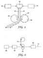
FIG. 5 is a schematic diagram of a portion of one manufacturing process according to the present invention. -
FIG. 6 is a schematic diagram of a system for manufacturing processing devices according to the present invention. -
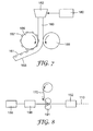
FIG. 7 is a schematic diagram of a portion of another manufacturing process according to the present invention. -
FIG. 8 is a schematic diagram of a system for manufacturing processing devices according to the present invention. - In the following detailed description of illustrative embodiments, reference is made to the accompanying figures of the drawing which form a part hereof, and in which are shown, by way of illustration, specific embodiments in which the invention may be practiced. It is to be understood that other embodiments may be utilized and structural changes may be made without departing from the scope of the present invention.
- The present invention provides a sample processing device that can be used in the processing of liquid sample materials (or sample materials entrained in a liquid) in multiple process chambers to obtain desired reactions, e.g., PCR amplification, ligase chain reaction (LCR), self-sustaining sequence replication, enzyme kinetic studies, homogeneous ligand binding assays, and other chemical, biochemical, or other reactions that may, e.g., require precise and/or rapid thermal variations. More particularly, the present invention provides sample processing devices that include one or more process arrays, each of which include a loading chamber, a plurality of process chambers and a main conduit placing the process chambers in fluid communication with the loading chamber.
- Although various constructions of illustrative embodiments are described below, sample processing devices of the present invention may be similar to those described in, e.g., International Publication Nos.
WO 02/01180 WO 02/00347 (both to Bedingham et al. - One illustrative sample processing device manufactured according to the principles of the present invention is illustrated in
FIGS. 1 & 2 , whereFIG. 1 is a perspective view of onesample processing device 10 andFIG. 2 is an enlarged plan view of a portion of thesample processing device 10. In both views, a cover (described below in connection withFIG. 3 ) has been removed to expose structures formed in thebody 60 of thedevice 10. - The
sample processing device 10 includes at least one, and preferably a plurality of process arrays 20. Each of the depicted process arrays 20 preferably extends from proximate afirst end 12 towards thesecond end 14 of thesample processing device 10. The process arrays 20 are depicted as being substantially parallel in their arrangement on thesample processing device 10. Although this arrangement may be preferred, it will be understood that any arrangement of process arrays 20 may alternatively be preferred. - Alignment of the process arrays 20 as depicted may be useful if the
main conduits 40 of the process arrays are to be closed simultaneously as discussed in, e.g., International Publication No.WO 02/01180 first end 12 of thedevice 10 as discussed in, e.g., International Publication No.WO 02/01180 - Each of the process arrays 20 in the depicted embodiment includes at least one
main conduit 40, and a plurality ofprocess chambers 50 located along eachmain conduit 40. The process arrays 20 may also preferably include a loading structure in fluid communication with amain conduit 40 to facilitate delivery of sample material to theprocess chambers 50 through themain conduit 40. It may be preferred that, as depicted inFIG. 1 , each of the process arrays include only oneloading structure 30 and only onemain conduit 40. - The
loading structure 30 may be designed to mate with an external apparatus (e.g., a pipette, hollow syringe, or other fluid delivery apparatus) to receive the sample material. Theloading structure 30 itself may define a volume or it may define no specific volume, but, instead, be a location at which sample material is to be introduced. For example, the loading structure may be provided in the form of a port through which a pipette or needle is to be inserted. In one embodiment, the loading structure may be, e.g., a designated location along the main conduit that is adapted to receive a pipette, syringe needle, etc. The loading may be performed manually or by an automated system (e.g., robotic, etc.). Further, theprocessing device 10 may be loaded directly from another device (using an automated system or manually). - The loading chamber depicted in
FIG. 1 is only one embodiment of aloading structure 30 in fluid communication with themain conduit 40. It may be preferred that the loading chamber volume, i.e., the volume defined by the loading chamber (if so provided), be equal to or greater than the combined volume of themain conduit 40,process chambers 50, and feeder conduits 42 (if any). - The
process chambers 50 are in fluid communication with themain conduit 40 throughfeeder conduits 42. As a result, theloading structure 30 in each of the process arrays 20 is in fluid communication with each of theprocess chambers 50 located along themain conduit 40 leading to theloading structure 30. If desired, each of the process arrays 20 may also include an optional drain chamber (not shown) located at the end of themain conduit 40 opposite theloading structure 30. -
FIG. 3 is a cross-sectional view of the portion of theprocessing device 10 depicted inFIG. 2 taken along line 3-3 inFIG. 2 . Theprocessing device 10 includes abody 60 that includes atransmissive layer 62 andcontrol layer 64. Thetransmissive layer 62 andcontrol layer 64 are attached by a melt bond. As used herein, a "melt bond" is a bond formed by the melting and/or mixing of materials such as that occurring during, e.g., heat sealing, thermal welding, ultrasonic welding, chemical welding, solvent bonding, coextrusion, extrusion casting, etc. In such a bond, the materials facing each other intransmissive layer 62 andcontrol layer 64 must be compatible with melt bonding so that an attachment of sufficient integrity can be formed to withstand the forces experienced during processing of sample materials in the process chambers. - The
transmissive layer 62 is constructed of one or more polymeric materials such that thetransmissive layer 62 transmits significant portions of selected light. For the purposes of the present invention, significant portions may be, e.g., 50% or more of normal incident selected light, more preferably 75% or more of normal incident selected light. As discussed above, the selected light may be light of one or more particular wavelengths, one or more ranges of wavelengths, one or more polarization states, or combinations thereof. Examples of some suitable materials for thetransmissive layer 62 include, but are not limited to, e.g., polypropylenes, polyesters, polycarbonates, polyethylenes, polypropylene-polyethylene copolymers, cyclo-olefin polymers (e.g., polydicyclopentadiene). - The
control layer 64 is constructed of one or more polymeric materials such that thecontrol layer 64 blocks significant portions of selected light. For the purposes of the present invention, significant portions of blocked light may be, e.g., 50% or more of normal incident selected light, more preferably 75% or more of normal incident selected light, and even more preferably 90% or more of normal incident selected light. As discussed above, the selected light may be one or more particular wavelengths, one or more ranges of wavelengths, one or more polarization states, or combinations thereof. Examples of some suitable materials for thecontrol layer 64 include, but are not limited to, e.g., polypropylenes, polyesters, polycarbonates, polyethylenes, polypropylene-polyethylene copolymers, cyclo-olefin polymers (e.g., polydicyclopentadiene), etc., that have been modified to provide the desired light blocking function. For example, the material used for thecontrol layer 64 may include a light blocking filler (e.g., colorants, carbon black, metallic particles, etc.) to prevent or reduce transmission of selected light through thecontrol layer 64. In other instances, thecontrol layer 64 may include a coating or other treatment that provides the desired light blocking function. - Since a melt bond between
transmissive layer 62 andcontrol layer 64 is to be formed, it may be preferred that thetransmissive layer 62 and thecontrol layer 64 be formed of compatible materials, in some instances, it may be preferred that thetransmissive layer 62 and thecontrol layer 64 be formed of the same polymeric material. - The
processing device 10 includesprocess chambers 50 and amain conduit 40 located between thebody 60 and thecover sheet 70. Coversheet 70 is attached to the surface 65 of thecontrol layer 64 facing away from thetransmissive layer 62 usingadhesive 72. Thecover sheet 70 may, however, be attached to thecontrol layer 64 by any suitable technique or combination of techniques, e.g., adhesives, combinations of melt bonding and adhesives, etc. Examples of some suitable attachment techniques may be described in, e.g., International Publication No.WO 02/01180 - The
process chambers 50 are, in the depicted embodiment, defined by process chamber structures formed in thecontrol layer 64 of thebody 60 and thecover sheet 70 attached to thecontrol layer 64. In the depicted embodiment, the process chamber structures are in the form of voids formed through thecontrol layer 64, the voids including interior side surfaces 52. Aninterior window surface 54 is also formed within theprocess chamber 50 by a portion of thetransmissive layer 62 exposed by the void in thecontrol layer 64. As such, theprocess chambers 50 may be described as having a height measured from thecover sheet 70 to theinterior window surface 54. Furthermore, it may be preferred that thecontrol layer 64 have a thickness between thecover sheet 70 and thetransmissive layer 62 that is less than or equal to the height of eachprocess chamber 50. If the height of theprocess chamber 50 is greater than the thickness of thecontrol layer 64, thetransmissive layer 62 may preferably be thinned or otherwise deformed in the area of thewindow surface 54. - Although the depicted process chamber structure is formed as a void that exposes a portion of the
transmissive layer 62 within theinterior window surface 54, it should be understood that, in some instances, it may be acceptable if a relatively thin portion of thecontrol layer 64 remains in the area occupied by thewindow surface 54. Any such relatively thin portion of thecontrol layer 64 should, however, be sufficiently thin such that transmission of the selected light through thewindow surface 54 is still possible. - The process chamber structure also preferably includes one or more interior side surfaces 52 as depicted that are formed by the
control layer 64. The interior side surfaces 52 may take any suitable shape, although it may be preferred that they extend from one major surface of thecontrol layer 64 to the opposite major surface of thecontrol layer 64. -
FIG. 3 also depicts that theprocess chambers 50 may include areagent 58 located therein. It may be preferred that at least some, and preferably all, of theprocess chambers 50 in thedevices 10 of the present invention contain at least one reagent before thecover sheet 70 is attached to thebody 60. Thereagent 58 may be fixed within theprocess chamber 50 as depicted inFIG. 3 or it may be loose within theprocess chamber 50. Thereagent 58 is optional, i.e.,sample processing devices 10 of the present invention may or may not include anyreagents 58 in theprocess chambers 50. In another variation, some of theprocess chambers 50 may include areagent 58, while others do not. In yet another variation,different process chambers 50 may contain different reagents (in which case it may be desirable to fix the reagents to a surface within each process chamber 50). Further, the interior of the process chamber structures may be coated or otherwise processed to control the adhesion ofreagents 58. Also, in some instances, reagents may be provided on thecover sheet 70. - Although the
cover sheet 70 is depicted as generally flat, it should be understood that thecover sheet 70 may deviate from a flat sheet if so desired. For example, thecover sheet 70 may be formed to increase or decrease the volume of theprocess chamber 50. - The
cover sheet 70 may be provided as, e.g., a sheet of metal foil, polymeric material, multi-layer composite, etc. that is attached to thecontrol layer 64 over theprocess chamber structures 52 to formprocess chambers 50. Although thecover sheet 70 is depicted as a unitary homogenous layer, it should be understood that thecover sheet 70 may include one or materials and those materials may be provided in different layers or they may be intermixed within thecover sheet 70. - If the
cover sheet 70 includes a metallic foil, thecover sheet 70 may preferably include a passivation layer on the surfaces that face the interiors of theprocess chambers 50 andmain conduit 40 to prevent contamination of the sample materials by the metal. As an alternative to a separate passivation layer, anyadhesive layer 72 used to attached thecover sheet 70 to thecontrol layer 64 may also serve as a passivation layer to prevent contact between the sample materials and any metallic layer in thecover sheet 70. Thecover sheet 70 may preferably be deformable such that themain conduits 40 can be closed or sealed as described in, e.g., International Publication No.WO 02/01180 - In some embodiments, it may be preferred that the
cover sheet 70 and adhesive 72 (if present) provide a reflective surface facing the interior of theprocess chambers 50 for the selected light. The reflectivity may be provided by, e.g., a metallic surface of thecover sheet 70, by the adhesive 72 itself, or by a reflective polymeric sheet used to form thecover sheet 70, or any other reflective structure or material. - In other embodiments, it may be preferred that the
cover sheet 70 be transmissive such that it transmits the selected light. In such an embodiment, theprocess chambers 50 may be interrogated by light that may be absorbed by one or more components within theprocess chamber 50. If both thetransmissive layer 62 and thecover 70 are transmissive to the selected light, a detector could be positioned on the side of the processing device opposite from the side at which the selected light is directed into theprocess chamber 50. For example, if the selected light is directed into theprocess chamber 50 through thetransmissive layer 62, the detector may be placed on the same side as thecover 70 such that the selected light is either absorbed within theprocess chamber 50 or transmitted through thetransmissive layer 62,process chamber 50 and cover 70 before reaching the detector. Such absorption may be used to determine the presence or absence of one or more analytes within theprocess chamber 50. Alternatively, signal light from, e.g., chemiluminescence in theprocess chamber 50 may be transmitted out of theprocess chamber 50 through either thetransmissive layer 62 or thetransmissive cover 70. - A variety of
adhesives 72 may be used, although any adhesive selected should be capable of withstanding the forces generated during processing of any sample materials located in theprocess chambers 50, e.g., forces developed during distribution of the sample materials, forces developed during thermal processing of the sample materials, etc. Those forces may be large where, e.g., the processing involves thermal cycling as in, e.g., polymerase chain reaction and similar processes. It may also be preferred that any adhesives used in connection with the sample processing devices exhibit low fluorescence, be compatible with the processes and materials to be used in connection with sample processing devices, e.g. PCR, etc. - It may be preferred to use adhesives that exhibit pressure sensitive properties. Such adhesives may be more amenable to high volume production of sample processing devices since they typically do not involve the high temperature bonding processes used in melt bonding, nor do they present the handling problems inherent in use of liquid adhesives, solvent bonding, ultrasonic bonding, and the like. Techniques for identifying and selecting pressure sensitive adhesives are discussed in, e.g., International Publication No.
WO 02/01180 - It may be preferred that the pressure sensitive adhesives used in connection with the sample processing devices of the present invention include materials which ensure that the properties of the adhesive are not adversely affected by water. For example, the pressure sensitive adhesive will preferably not lose adhesion, lose cohesive strength, soften, swell, or opacify in response to exposure to water during sample loading and processing. Also, the pressure sensitive adhesive should not contain any components which may be extracted into water during sample processing, thus possibly compromising the device performance.
- In view of these considerations, it may be preferred that the pressure sensitive adhesive be composed of hydrophobic materials. As such, it may be preferred that the pressure sensitive adhesive be composed of silicone materials. Some suitable compositions may be described in International Publication
WO 00/68336 - Also depicted in the embodiment of
FIG. 3 is a cross-sectional view of themain conduit 40 that is in fluid communication with theprocess chambers 50. Themain conduit 40, in the depicted embodiment, is defined byconduit structure 44 formed in thecontrol layer 64 of thebody 60 and thecover sheet 70 attached to thecontrol layer 64. In the depicted embodiment, theconduit structure 44 is in the form of a channel formed into the surface of thecontrol layer 64 facing away from thetransmissive layer 62. As such, theconduit structure 44 may be described as having a height measured from thecover sheet 70 towards thetransmissive layer 62. Furthermore, it may be preferred that the height of theconduit structure 44 be less than the thickness of the control layer 64 (as measured between the opposing major surfaces of the control layer 64) such that, e.g., none of thetransmissive layer 62 be exposed within theconduit structure 44. - Although the
cover sheet 70 is depicted as generally flat, it should be understood that thecover sheet 70 may deviate from a flat sheet if so desired. For example, thecover sheet 70 may be formed to increase or decrease the cross-sectional area of the conduit 40 (in the view as seen inFIG. 3 ). - Further, it may be preferred that the shape of the
conduit structure 44 and the materials selected for thecontrol layer 64, thecover sheet 70 and the adhesive 72 be such that theconduit 40 can be sealed or occluded by deforming thecover sheet 70 into theconduit structure 44 as described in, e.g., International Publication No.WO 02/01180 -
FIG. 4 depicts an alternative construction for a sample processing device according to the present invention. The processing device is formed by abody 160 and acover sheet 170. In this embodiment, however, thebody 160 is formed of a material or materials that block the transmission of selected light between theprocess chambers 150. - Transmission of the selected light into and/or out of the
process chambers 150 occurs, instead, through thecover sheet 170 which transmits significant portions of the selected light. For the purposes of the present invention, significant portions may be, e.g., 50% or more of normal incident selected light, more preferably 75% or more of normal incident selected light. As discussed above, the selected light may be one or more particular wavelengths, one or more ranges of wavelengths, one or more polarization states, or combinations thereof. Examples of some suitable materials for thecover sheet 170 include, but are not limited to, e.g., polypropylenes, polyesters, polycarbonates, polyethylenes, polypropylene-polyethylene copolymers, cyclo-olefin polymers (e.g., polydicyclopentadiene), etc. - Although the
cover sheet 170 is depicted as a unitary homogenous layer, it should be understood that thecover sheet 170 may include one or materials and those materials may be provided in different layers or they may be intermixed within thecover sheet 170. - The
body 160 is preferably constructed of one or more materials such that thebody 160 blocks transmission of significant portions of selected light. For the purposes of the present invention, significant portions of blocked light may be, e.g., 50% or more of normal incident selected light, more preferably 75% or more of normal incident select light, and even more preferably 90% or more of normal incident selected light. As discussed above, the selected light may be one or more particular wavelengths, one or more ranges of wavelengths, one or more polarization states, or combinations thereof. - Examples of some suitable materials for the
body 160 include, but are not limited to, e.g., polypropylenes, polyesters, polycarbonates, polyethylenes, polypropylene-polyethylene copolymers, cyclo-olefin polymers (e.g., polydicyclopentadiene), etc., that have been modified to provide the desired light blocking function. For example, the material used for thebody 160 may include a light blocking filler (e.g., colorants, carbon black, metallic particles, etc.) to prevent or reduce transmission of selected light through thebody 160. In other instances, thebody 160 may include a coating or other treatment that provides the desired light blocking function. - The processing device includes
process chambers 150 and amain conduit 140 located between thebody 160 and thecover sheet 170. Theprocess chambers 150 are, in the depicted embodiment, defined by process chamber structures 152 formed in thesurface 161 ofbody 160 and thecover sheet 170 attached to thebody 160. In the depicted embodiment, the process chamber structures 152 are in the form of depressions formed into the body, but not through the entire thickness of thebody 160. Although thecover sheet 170 is depicted as generally flat, it should be understood that thecover sheet 170 may deviate from a flat sheet if so desired. For example, thecover sheet 170 may be formed to increase or decrease the volume of theprocess chamber 150. -
Cover sheet 170 is attached to thesurface 161 of thebody 160 using adhesive 172. Thecover sheet 170 may, however, be attached to thebody 160 by any suitable technique or combination of techniques, e.g., adhesives, combinations of melt bonding and adhesives, etc. Examples of some suitable attachment techniques may be described above with respect to adhesive 72 oncover sheet 70 inFIG. 3 , as well as in, e.g., International Publication No.WO 02/01180 - Also depicted in the embodiment of
FIG. 4 is a cross-sectional view of themain conduit 140 that is in fluid communication with theprocess chambers 150. Themain conduit 140, in the depicted embodiment, is defined byconduit structure 144 formed in thebody 160 and thecover sheet 170 attached to thebody 160. In the depicted embodiment, theconduit structure 144 is in the form of a channel formed into thesurface 161 facing thecover sheet 170. As such, theconduit structure 144 may be described as having a height measured from thecover sheet 170 towards the opposingsurface 163 of thebody 160. Furthermore, it may be preferred that the height of theconduit structure 144 be less than the thickness of thebody 160 as measured between oppositemajor surfaces - The processing devices of the present invention may be manufactured by a variety of methods and techniques. A portion of one exemplary manufacturing method is depicted in
FIG. 5 for manufacturing processing devices including a body having a transmissive layer and control layer as described in connection withFIG. 3 . A melt-processable polymer for thetransmissive layer 62 is delivered from anextruder 80 to multi-layer feedblock and film die 82. At the same time, a melt-processable polymer for thecontrol layer 64 is delivered fromextruder 84 the multi-layer feedblock and film die 82. The two melt-processable polymers streams are delivered to the multi-layer feedblock and film die 82 at or above their melt-processing temperature. The multi-layer feedblock and film die 82 preferably keeps the two polymer melt streams fromextruders discrete layers - The
layers tool 86. It may be preferred that the polymers be drop cast onto the surface of the formingtool 86 at a point near the nip between formingtool 86 andbackup roll 88. - The forming
tool 86 includesprotrusions 87 extending therefrom that correspond to the various features to be formed in the processing devices, e.g., process chambers, conduits, etc. It may be preferred that the thickness of each oflayers layer 64 is less than or equal to the height of theprotrusions 87 that form the process chamber structures in the processing devices of the present invention. Limiting the thickness oflayer 64 in that manner can provide for process chamber structures inlayer 64 that are formed as voids as described above with respect toFIG. 3 . - It may be preferred that at least the
control layer 64 be delivered to the formingtool 86 at a temperature that is at or above its melt processing temperature (i.e., the temperature at which it can be formed or molded). By providing thecontrol layer 64 to the formingtool 86 at or above its melt processing temperature, the polymer in the control layer can adequately form or be replicated to the shape of theprotrusions 87 on the formingtool 86. Although the formingtool 86 is depicted as a roll, it should be understood that it may alternatively be provided as a continuous belt or other structure amenable to continuous web-form processing. - It may also be preferred that the polymer of the
transmissive layer 62 also be delivered to the nip formed by formingtool 86 andbackup roll 88 at a temperature that is at or above its melt processing temperature such that the twolayers tool 86 are being formed into thecontrol layer 64. - The temperatures of both
layers backup roll 88 to retain the structures formed inlayer 64 and provide mechanical stability to the web. - The result of the processing depicted in
FIG. 5 is a web including both atransmissive layer 62 andcontrol layer 64 to form thebody 60 of a processing device according to the present invention. Thecontrol layer 64 includes structures formed therein for, e.g., process chambers, conduits, loading chambers, etc. -
FIG. 6 is a schematic diagram of the larger process for manufacturing processing devices according to the present invention. The system depicted inFIG. 6 includes the components and process ofFIG. 5 asapparatus 89. The web formed by apparatus 89 (including the transmissive layer and the control layer 64) may preferably be fed into areagent station 90 where reagents can be added to, e.g., the process chamber structures as discussed herein. Following the addition of reagents, the web may preferably be fed into alaminating station 91 where acover sheet web 70 is laminated thereto to form a composite web structure includingprocess chambers 50,conduits 40, etc. The composite web may then preferably be delivered to asheeting station 92 where the web is separated by, e.g., die cutting, intoindividual processing devices 10. -
FIGS. 7 & 8 depict an alternative manufacturing process that may be used to, e.g., manufacture processing devices constructed as described inFIG. 4 . The A melt-processable polymer for thebody 160 is delivered from anextruder 180 to die 182. The melt-processable polymer stream is delivered to the die 182 at or above its melt-processing temperature. - The
polymer layer 160 is discharged from thedie 182 onto a formingtool 186. It may be preferred that thelayer 160 be drop cast onto the formingtool 186 just before the nip formed withbackup roll 188. The formingtool 186 includesprotrusions 187 extending therefrom that correspond to the various features to be formed in the processing devices, e.g., process chambers, conduits, etc. It is preferred that the thickness of thepolymer layer 160 be controlled such that the thickness oflayer 160 is greater than the height of theprotrusions 187 that form the process chamber structures in the processing devices of the present invention. - It may be preferred that the
polymer layer 160 be delivered to the formingtool 186 at a temperature that is at or above its melt processing temperature (i.e., the temperature at which it can be formed or molded). By providing thepolymer layer 160 to the formingtool 186 at or above its melt processing temperature, the polymer can adequately form or be replicated to the shape of theprotrusions 187 on the formingtool 186. Although the formingtool 186 is depicted as a roll, it should be understood that it may alternatively be provided as a continuous belt or other structure amenable to continuous web-form processing. - The temperature of the
polymer layer 160 is preferably lowered to below the melt processing temperature at some point after the nip withbackup roll 188 to retain the structures fonned inlayer 160 and provide mechanical stability to the web. The result of the processing depicted inFIG. 7 is aweb 160 that can be used to form the bodies of processing devices according to the present invention. Theweb 160 includes structures formed therein for, e.g., process chambers, conduits, loading chambers, etc. -
FIG. 8 is a schematic diagram of the larger process for manufacturing processing devices according to the present invention. The system depicted inFIG. 8 includes the components and process ofFIG. 7 asapparatus 189. The web formed byapparatus 189 may preferably be fed into areagent station 190 where reagents can be added to, e.g., the process chamber structures as discussed herein. Following the addition of reagents, the web may preferably be fed into alaminating station 191 where acover sheet web 170 is laminated thereto to form a composite web structure including process chambers, conduits, etc. The composite web may then preferably be delivered to asheeting station 192 where the web is separated by, e.g., die cutting, intoindividual processing devices 110. - In an alternative process, the web formed by
apparatus 189 may be sheeted before any reagents are added to the sheeted web. It may also be preferred that in such a process, thecover sheet web 170 be sheeted before it is laminated to the sheets formed from the web ofapparatus 189. - Illustrative embodiments of this invention are discussed and reference has been made to possible variations within the scope of this invention. It should be understood that this invention is not limited to the illustrative embodiments set forth herein. Accordingly, the invention is to be limited only by the claims provided below.
Claims (35)
- A sample processing device (10) comprising:a polymeric body comprising a polymeric transmissive layer (62) that transmits selected light and a polymeric control layer (64) that blocks the selected light, wherein the control layer is melt-bonded to the transmissive layer with a first major surface of the control layer facing the transmissive layer and a second major surface facing away from the transmissive layer;a plurality of process chamber structures (50) formed in the control layer, wherein each of the process chamber structures comprises an interior window surface (54) and an interior side surface (52) formed by the control layer;a cover sheet (70) attached to the second major surface of the control layer, wherein the cover sheet and the plurality of process chamber structures define a plurality of process chambers (50) in the sample processing device, wherein the selected light can be transmitted into or out of each process chamber through the interior window surface; anda conduit (40, 42) in the sample processing device, wherein each process chamber of the plurality of process chambers is in fluid communication with the conduit.
- A device according to claim 1, wherein each of the process chamber structures comprises a void formed through the first major surface and the second major surface of the control layer, wherein the void exposes the interior window surface formed by the transmissive layer.
- A device according to claim 1, wherein the interior window surface within each process chamber is formed by the transmissive layer.
- A device according to any one of claims 1-3, wherein the transmissive layer arid the control layer comprise the same polymeric material, and further wherein the control layer comprises a light blocking filler incorporated therein.
- A device according to any one of claims 1-4, wherein each process chamber of the plurality of process chambers comprises a height measured from the cover sheet to the interior window surface, and wherein the control layer comprises a thickness between the cover sheet and the transmissive layer that is less than or equal to the height of each process chamber of the plurality of process chambers.
- A device according to any one of claims 1-5, wherein the conduit is formed between the cover sheet and the control layer.
- A device according to any one of claims 1-5, wherein the conduit comprises a conduit structure formed in the second major surface of the control layer, wherein the cover sheet and the conduit structure define the conduit in the sample processing device.
- A device according to claim 7, wherein the conduit structure comprises a depth measured from the second major surface of the control layer that is less than a thickness of the control layer as measured between the first major surface and the second major surface of the control layer.
- A device according to any one of claims 1-8, wherein the cover sheet blocks the selected light.
- A device according to any one of claims 1-9, wherein the cover sheet comprises a reflective surface facing the control layer.
- A device according to any one of claims 1-8, wherein the cover sheet transmits the selected light.
- A method of manufacturing a sample processing device, the method comprising:providing a body that comprises:a polymeric transmissive layer that transmits selected light;a polymeric control layer that blocks the selected light, wherein the control layer is melt-bonded to the transmissive layer with a first major surface of the control layer facing the transmissive layer and a second major surface facing away from the transmissive layer;a plurality of process chamber structures formed in the control layer, wherein each of the process chamber structures comprises an interior window surface and an interior side surface formed by the control layer; andattaching a cover sheet to the second major surface of the control layer,wherein the cover sheet and the plurality of process chamber structures define a plurality of process chambers in the sample processing device, and wherein attaching the cover sheet forms a conduit in the sample processing device, wherein each process chamber of the plurality of process chambers is in fluid communication with the conduit.
- A method according to claim 12, wherein providing the body comprises forming a void through the control layer to form each process chamber structure of the plurality of process chamber structures, wherein forming the void exposes the interior window surface of the process chamber.
- A method according to claim 13, wherein, for each process chamber structure, forming the void comprises exposing the transmissive layer to form the interior window surface.
- A method according to any one of claims 12-14, wherein providing the body comprises forming the plurality of process chamber structures into the control layer.
- A method according to claim 15, wherein forming the plurality of process chamber structures comprises:providing the control layer on the transmissive layer, wherein the control layer comprises polymeric material at or above a melt processing temperature of the polymeric material;forming the plurality of process chamber structures into the control layer while the control layer is held at or above the melt processing temperature; andlowering the temperature of the control layer below the melt processing temperature after forming the plurality of process chamber structures.
- A method according to any one of claims 12-16, wherein the conduit is formed between the cover sheet and the control layer.
- A method according to any one of claims 12-16, wherein the conduit comprises a conduit structure formed in the second major surface of the control layer, wherein the cover sheet and the conduit structure define the conduit in the sample processing device.
- A method according to claim 18, wherein forming the conduit structure comprises:providing the control layer on the transmissive layer, wherein the control layer comprises polymeric material at or above a melt processing temperature of the polymeric material;forming the conduit structure in the control layer while the control layer is held at or above the melt processing temperature; andlowering the temperature of the control layer below the melt processing temperature after forming the conduit structure.
- A method according to any one of claims 18-19, wherein the conduit structure comprises a depth measured from the second major surface of the control layer that is less than a thickness of the control layer as measured between the first major surface and the second major surface of the control layer.
- A method according to any one of claims 12-20, further comprising locating one or more reagents in one or more of the process chamber structures before attaching the cover sheet.
- A method according to any one of claims 12-21, wherein each process chamber of the plurality of process chambers comprises a height measured from the cover sheet to the interior window surface, and wherein the control layer comprises a thickness between the cover sheet and the transmissive layer that is less than or equal to the height of each process chamber of the plurality of process chambers.
- A method according to any one of claims 12-22, wherein the interior window surface within each process chamber is formed by the transmissive layer.
- A method according to any one of claims 12-23, wherein the cover sheet blocks the selected light.
- A method according to any one of claims 12-23, wherein the cover sheet comprises a reflective surface facing the control layer.
- A method according to any one of claims 12-23, wherein the cover sheet transmits the selected light.
- A sample processing device comprising:a polymeric body (160) comprising a first major surface and a second major surface, wherein the second major surface is flat, and wherein the polymeric body blocks selected light;a plurality of process chamber structures (150) formed in the body, wherein the process chamber structures are formed into the first major surface of the body;a cover sheet (170) attached to the first major surface of the body, wherein the cover sheet and the plurality of process chamber structures define a plurality of process chambers (150) in the sample processing device, and wherein the cover sheet transmits the selected light; anda conduit (140) located between the body and the cover sheet, wherein each process chamber of the plurality of process chambers is in fluid communication with the conduit.
- A device according to claim 27, wherein the conduit comprises conduit structure formed in the first major surface of the body, wherein the cover sheet and the conduit structure define the conduit in the sample processing device.
- A device according to any one of claims 27-28, wherein the cover sheet is adhesively attached to the first major surface of the body.
- A method of manufacturing a sample processing device, the method comprising:providing a polymeric body that comprises a first major surface and a second major surface, wherein the second major surface is flat, and wherein the body blocks selected light, wherein the body further comprises a plurality of process chamber structures formed in the first major surface of the body; andattaching a cover sheet to the first major surface of the body, wherein the cover sheet and the plurality of process chamber structures define a plurality of process chambers in the sample processing device;and wherein attaching the cover sheet forms a conduit in the sample processing device, wherein each process chamber of the plurality of process chambers is in fluid communication with the conduit.
- A method according to claim 30, wherein the conduit is formed between the cover sheet and the first major surface of the body.
- A method according to any one of claims 30-31, wherein the conduit comprises a conduit structure formed in the first major surface of the body, wherein the cover sheet and the conduit structure define the conduit in the sample processing device.
- A method according to any one of claims 30-32, further comprising forming the conduit structure in the first major surface of the body.
- A method according to any one of claims 30-33, further comprising locating one or more reagents in one or more of the process chamber structures before attaching the cover sheet.
- A method according to any one of claims 30-34, wherein the cover sheet transmits the selected light.
Priority Applications (1)
| Application Number | Priority Date | Filing Date | Title |
|---|---|---|---|
| EP09176090A EP2181766A1 (en) | 2003-10-09 | 2004-08-16 | Multilayer sample processing devices and methods |
Applications Claiming Priority (2)
| Application Number | Priority Date | Filing Date | Title |
|---|---|---|---|
| US10/682,597 US7718133B2 (en) | 2003-10-09 | 2003-10-09 | Multilayer processing devices and methods |
| PCT/US2004/026546 WO2005039769A1 (en) | 2003-10-09 | 2004-08-16 | Multilayer sample processing devices and methods |
Publications (2)
| Publication Number | Publication Date |
|---|---|
| EP1682271A1 EP1682271A1 (en) | 2006-07-26 |
| EP1682271B1 true EP1682271B1 (en) | 2009-11-18 |
Family
ID=34422558
Family Applications (2)
| Application Number | Title | Priority Date | Filing Date |
|---|---|---|---|
| EP09176090A Withdrawn EP2181766A1 (en) | 2003-10-09 | 2004-08-16 | Multilayer sample processing devices and methods |
| EP04781263A Not-in-force EP1682271B1 (en) | 2003-10-09 | 2004-08-16 | Multilayer sample processing devices and methods |
Family Applications Before (1)
| Application Number | Title | Priority Date | Filing Date |
|---|---|---|---|
| EP09176090A Withdrawn EP2181766A1 (en) | 2003-10-09 | 2004-08-16 | Multilayer sample processing devices and methods |
Country Status (9)
| Country | Link |
|---|---|
| US (2) | US7718133B2 (en) |
| EP (2) | EP2181766A1 (en) |
| JP (2) | JP2007508542A (en) |
| CN (1) | CN1867406B (en) |
| AT (1) | ATE448876T1 (en) |
| AU (1) | AU2004283174B2 (en) |
| CA (1) | CA2541900A1 (en) |
| DE (1) | DE602004024229D1 (en) |
| WO (1) | WO2005039769A1 (en) |
Families Citing this family (12)
| Publication number | Priority date | Publication date | Assignee | Title |
|---|---|---|---|---|
| US7718133B2 (en) * | 2003-10-09 | 2010-05-18 | 3M Innovative Properties Company | Multilayer processing devices and methods |
| MX2007008664A (en) * | 2005-01-20 | 2007-09-06 | 3M Innovative Properties Co | Structured polymer films and methods for forming the same. |
| US20060157381A1 (en) * | 2005-01-20 | 2006-07-20 | Adams James T | Component carrier and method for making |
| US20060293438A1 (en) * | 2005-06-23 | 2006-12-28 | 3M Innovative Properties Company | Carrier tapes and compositions thereof |
| US20080087572A1 (en) * | 2006-10-17 | 2008-04-17 | 3M Innovative Properties Company | Component carrier and method for making |
| US10125388B2 (en) | 2007-10-31 | 2018-11-13 | Akonni Biosystems, Inc. | Integrated sample processing system |
| US8828912B2 (en) | 2009-09-21 | 2014-09-09 | Akonni Biosystems, Inc. | Method of making a microarray assembly |
| US8969029B2 (en) | 2008-10-17 | 2015-03-03 | 3M Innovative Properties Company | Biological sterilization indicator, system, and methods of using same |
| EP2504104A1 (en) | 2009-11-23 | 2012-10-03 | 3M Innovative Properties Company | Carrier with flexible microassay device and methods of use |
| WO2011108333A1 (en) * | 2010-03-05 | 2011-09-09 | コニカミノルタオプト株式会社 | Microfluidic detection chip manufacturing method |
| KR20170072188A (en) * | 2014-09-23 | 2017-06-26 | 티어랩 리서치, 인코포레이티드 | Systems and methods for integration of microfluidic tear collection and lateral flow analysis of analytes of interest |
| CN104841500B (en) * | 2015-05-12 | 2016-08-17 | 天津微纳芯科技有限公司 | A kind of chip for sample detection and method for packing thereof |
Family Cites Families (72)
| Publication number | Priority date | Publication date | Assignee | Title |
|---|---|---|---|---|
| US3856470A (en) | 1973-01-10 | 1974-12-24 | Baxter Laboratories Inc | Rotor apparatus |
| US3938958A (en) | 1975-03-24 | 1976-02-17 | Corning Glass Works | Fluid dispensing device |
| US4390499A (en) | 1981-08-13 | 1983-06-28 | International Business Machines Corporation | Chemical analysis system including a test package and rotor combination |
| US4673657A (en) | 1983-08-26 | 1987-06-16 | The Regents Of The University Of California | Multiple assay card and system |
| US4632908A (en) | 1984-05-03 | 1986-12-30 | Abbott Laboratories | Heating system for rotating members |
| US4806316A (en) | 1987-03-17 | 1989-02-21 | Becton, Dickinson And Company | Disposable device for use in chemical, immunochemical and microorganism analysis |
| US5229297A (en) | 1989-02-03 | 1993-07-20 | Eastman Kodak Company | Containment cuvette for PCR and method of use |
| US5089233A (en) | 1989-06-12 | 1992-02-18 | Eastman Kodak Company | Processing apparatus for a chemical reaction pack |
| CA1329698C (en) | 1989-06-12 | 1994-05-24 | Mark Joseph Devaney, Jr. | Temperature control device |
| US5346672A (en) | 1989-11-17 | 1994-09-13 | Gene Tec Corporation | Devices for containing biological specimens for thermal processing |
| US5258163A (en) | 1990-04-14 | 1993-11-02 | Boehringer Mannheim Gmbh | Test carrier for analysis of fluids |
| US5219526A (en) | 1990-04-27 | 1993-06-15 | Pb Diagnostic Systems Inc. | Assay cartridge |
| EP0533801B1 (en) | 1990-06-15 | 1994-08-10 | Chiron Corporation | Self-contained assay assembly and apparatus |
| US5154888A (en) | 1990-10-25 | 1992-10-13 | Eastman Kodak Company | Automatic sealing closure means for closing off a passage in a flexible cuvette |
| US5248479A (en) | 1990-11-16 | 1993-09-28 | Abbott Laboratories | Agglutination reaction device having geometrically modified chambers |
| US5254479A (en) | 1991-12-19 | 1993-10-19 | Eastman Kodak Company | Methods for preventing air injection into a detection chamber supplied with injected liquid |
| US5744366A (en) | 1992-05-01 | 1998-04-28 | Trustees Of The University Of Pennsylvania | Mesoscale devices and methods for analysis of motile cells |
| US5587128A (en) | 1992-05-01 | 1996-12-24 | The Trustees Of The University Of Pennsylvania | Mesoscale polynucleotide amplification devices |
| US5726026A (en) | 1992-05-01 | 1998-03-10 | Trustees Of The University Of Pennsylvania | Mesoscale sample preparation device and systems for determination and processing of analytes |
| US5319436A (en) * | 1992-05-28 | 1994-06-07 | Packard Instrument Company, Inc. | Microplate farming wells with transparent bottom walls for assays using light measurements |
| US5288463A (en) | 1992-10-23 | 1994-02-22 | Eastman Kodak Company | Positive flow control in an unvented container |
| US5422271A (en) | 1992-11-20 | 1995-06-06 | Eastman Kodak Company | Nucleic acid material amplification and detection without washing |
| DE69329424T2 (en) | 1992-11-06 | 2001-04-19 | Biolog Inc | TEST DEVICE FOR LIQUID AND SUSPENSION SAMPLES |
| US5425917A (en) | 1992-11-09 | 1995-06-20 | Schmid; Peter | Apparatus for attaching a labeled probe and/or antibody to macromolecules |
| WO1994026414A1 (en) | 1993-05-17 | 1994-11-24 | Syntex (U.S.A.) Inc. | Reaction container for specific binding assays and method for its use |
| US5639428A (en) | 1994-07-19 | 1997-06-17 | Becton Dickinson And Company | Method and apparatus for fully automated nucleic acid amplification, nucleic acid assay and immunoassay |
| US6001229A (en) | 1994-08-01 | 1999-12-14 | Lockheed Martin Energy Systems, Inc. | Apparatus and method for performing microfluidic manipulations for chemical analysis |
| CA2156226C (en) * | 1994-08-25 | 1999-02-23 | Takayuki Taguchi | Biological fluid analyzing device and method |
| US5585069A (en) | 1994-11-10 | 1996-12-17 | David Sarnoff Research Center, Inc. | Partitioned microelectronic and fluidic device array for clinical diagnostics and chemical synthesis |
| CA2204912C (en) | 1994-11-10 | 2005-01-04 | David Sarnoff Research Center, Inc. | Liquid distribution system |
| ES2178708T3 (en) | 1995-04-25 | 2003-01-01 | Minnesota Mining & Mfg | SEGMENTED COPOLIMEROS OF POLIDIORGANOSILOXANOS AND POLYUREA, AND A PROCEDURE TO OBTAIN THEM. |
| WO1996034028A1 (en) | 1995-04-25 | 1996-10-31 | Minnesota Mining And Manufacturing Company | Tackified polydiorganosiloxane oligourea segmented copolymers and a process for making same |
| US5849208A (en) * | 1995-09-07 | 1998-12-15 | Microfab Technoologies, Inc. | Making apparatus for conducting biochemical analyses |
| US5759494A (en) | 1995-10-05 | 1998-06-02 | Corning Incorporated | Microplates which prevent optical cross-talk between wells |
| KR100306951B1 (en) | 1995-12-05 | 2001-11-15 | 테칸 보스턴, 인코포레이티드 | Devices and method for using centripetal acceleration to drive fluid movement in a microfluidics system with on-board informatics |
| US5833923A (en) | 1995-12-22 | 1998-11-10 | Universal Healthwatch, Inc. | Sampling-assay interface system |
| US5863502A (en) | 1996-01-24 | 1999-01-26 | Sarnoff Corporation | Parallel reaction cassette and associated devices |
| US6399023B1 (en) | 1996-04-16 | 2002-06-04 | Caliper Technologies Corp. | Analytical system and method |
| US5863801A (en) | 1996-06-14 | 1999-01-26 | Sarnoff Corporation | Automated nucleic acid isolation |
| NZ333346A (en) | 1996-06-28 | 2000-03-27 | Caliper Techn Corp | High-throughput screening assay systems in microscale fluidic devices |
| US5804141A (en) | 1996-10-15 | 1998-09-08 | Chianese; David | Reagent strip slide treating apparatus |
| CN1232412A (en) * | 1996-11-06 | 1999-10-20 | 康宁股份有限公司 | Method and device for manufacture of plate of wells, notably for samples of chemical or biological products |
| US5811296A (en) | 1996-12-20 | 1998-09-22 | Johnson & Johnson Clinical Diagnostics, Inc. | Blocked compartments in a PCR reaction vessel |
| US5876675A (en) | 1997-08-05 | 1999-03-02 | Caliper Technologies Corp. | Microfluidic devices and systems |
| GB9804483D0 (en) | 1998-03-02 | 1998-04-29 | Central Research Lab Ltd | Apparatus for and method of controlling the rate of flow of fluid along a pathway |
| DE59905743D1 (en) | 1998-03-11 | 2003-07-03 | Steag Microparts Gmbh | SAMPLE CARRIER |
| US7097974B1 (en) * | 1998-08-28 | 2006-08-29 | Febit Biotech Gmbh | Support for a method for determining an analyte and a method for producing the support |
| JP2002525600A (en) | 1998-09-22 | 2002-08-13 | セロミックス インコーポレイテッド | Miniaturized cell array method and device for cell-based screening |
| US6572830B1 (en) | 1998-10-09 | 2003-06-03 | Motorola, Inc. | Integrated multilayered microfludic devices and methods for making the same |
| JP3511910B2 (en) * | 1998-10-14 | 2004-03-29 | 株式会社島津製作所 | Detector cell |
| WO2000067037A2 (en) * | 1999-04-29 | 2000-11-09 | Dade Microscan Inc. | A combined rapid anti-microbial susceptibility assay and microorganism identification system |
| WO2000068336A1 (en) | 1999-05-05 | 2000-11-16 | 3M Innovative Properties Company | Silicone adhesives, articles, and methods |
| WO2001007892A1 (en) | 1999-07-27 | 2001-02-01 | Esperion Therapeutics, Inc. | Method and device for measurement of cholesterol efflux |
| US6586257B1 (en) * | 1999-10-12 | 2003-07-01 | Vertex Pharmaceuticals Incorporated | Multiwell scanner and scanning method |
| JP4327970B2 (en) * | 1999-12-28 | 2009-09-09 | 浜松ホトニクス株式会社 | Luminescence measuring apparatus and fluorescence measuring apparatus |
| JP3510882B2 (en) * | 2000-06-20 | 2004-03-29 | 三菱レイヨン株式会社 | Biologically related substance microarray and manufacturing method thereof |
| ES2449445T3 (en) | 2000-06-28 | 2014-03-19 | 3M Innovative Properties Co. | Improved devices, systems and methods for the treatment of samples |
| JP4773035B2 (en) * | 2000-06-28 | 2011-09-14 | スリーエム イノベイティブ プロパティズ カンパニー | Enhanced sample processing apparatus, system and method |
| US6734401B2 (en) * | 2000-06-28 | 2004-05-11 | 3M Innovative Properties Company | Enhanced sample processing devices, systems and methods |
| US6627159B1 (en) | 2000-06-28 | 2003-09-30 | 3M Innovative Properties Company | Centrifugal filling of sample processing devices |
| EP1373874A4 (en) | 2001-01-31 | 2004-03-31 | Univ Texas | Method and apparatus for the confinement of materials in a micromachined chemical sensor array |
| WO2003056517A1 (en) | 2001-12-31 | 2003-07-10 | Gyros Ab | Method and arrangement for reducing noise in a microfluid device |
| JP3775305B2 (en) * | 2002-01-31 | 2006-05-17 | コニカミノルタホールディングス株式会社 | Liquid mixing mechanism and liquid mixing method |
| JP2003279471A (en) * | 2002-03-20 | 2003-10-02 | Nippon Sheet Glass Co Ltd | Chip for microchemical system and microchemical system |
| US20030183958A1 (en) | 2002-03-28 | 2003-10-02 | Becton, Dickinson And Company | Multi-well plate fabrication |
| US7198759B2 (en) | 2002-07-26 | 2007-04-03 | Applera Corporation | Microfluidic devices, methods, and systems |
| US7201881B2 (en) | 2002-07-26 | 2007-04-10 | Applera Corporation | Actuator for deformable valves in a microfluidic device, and method |
| US7135147B2 (en) | 2002-07-26 | 2006-11-14 | Applera Corporation | Closing blade for deformable valve in a microfluidic device and method |
| US7507376B2 (en) | 2002-12-19 | 2009-03-24 | 3M Innovative Properties Company | Integrated sample processing devices |
| US7718133B2 (en) * | 2003-10-09 | 2010-05-18 | 3M Innovative Properties Company | Multilayer processing devices and methods |
| AU2008101286A4 (en) * | 2007-05-14 | 2011-12-15 | Erie Scientific Company | Multiwell plate device |
| JOP20210043A1 (en) | 2015-10-01 | 2017-06-16 | Arrowhead Pharmaceuticals Inc | Compositions and Methods for Inhibiting Gene Expression of LPA |
-
2003
- 2003-10-09 US US10/682,597 patent/US7718133B2/en not_active Expired - Fee Related
-
2004
- 2004-08-16 EP EP09176090A patent/EP2181766A1/en not_active Withdrawn
- 2004-08-16 WO PCT/US2004/026546 patent/WO2005039769A1/en active Search and Examination
- 2004-08-16 JP JP2006533851A patent/JP2007508542A/en active Pending
- 2004-08-16 CN CN200480029758.2A patent/CN1867406B/en not_active Expired - Fee Related
- 2004-08-16 AU AU2004283174A patent/AU2004283174B2/en not_active Ceased
- 2004-08-16 DE DE602004024229T patent/DE602004024229D1/en active Active
- 2004-08-16 CA CA002541900A patent/CA2541900A1/en not_active Abandoned
- 2004-08-16 AT AT04781263T patent/ATE448876T1/en not_active IP Right Cessation
- 2004-08-16 EP EP04781263A patent/EP1682271B1/en not_active Not-in-force
-
2010
- 2010-02-04 JP JP2010022869A patent/JP5086381B2/en not_active Expired - Fee Related
- 2010-03-30 US US12/749,763 patent/US8865091B2/en not_active Expired - Fee Related
Also Published As
| Publication number | Publication date |
|---|---|
| AU2004283174A1 (en) | 2005-05-06 |
| US20050079101A1 (en) | 2005-04-14 |
| CN1867406B (en) | 2010-06-16 |
| US20100183479A1 (en) | 2010-07-22 |
| WO2005039769A1 (en) | 2005-05-06 |
| JP2007508542A (en) | 2007-04-05 |
| ATE448876T1 (en) | 2009-12-15 |
| JP5086381B2 (en) | 2012-11-28 |
| AU2004283174B2 (en) | 2010-01-07 |
| EP1682271A1 (en) | 2006-07-26 |
| EP2181766A1 (en) | 2010-05-05 |
| JP2010122237A (en) | 2010-06-03 |
| US7718133B2 (en) | 2010-05-18 |
| CA2541900A1 (en) | 2005-05-06 |
| US8865091B2 (en) | 2014-10-21 |
| CN1867406A (en) | 2006-11-22 |
| DE602004024229D1 (en) | 2009-12-31 |
Similar Documents
| Publication | Publication Date | Title |
|---|---|---|
| US8865091B2 (en) | Multilayer processing devices and methods | |
| US7322254B2 (en) | Variable valve apparatus and methods | |
| CA2527534C (en) | Packaging of microfluidic devices | |
| EP1846159B1 (en) | Microfluidic cartridge with reservoirs for increased shelf life of installed reagents | |
| CN101674888B (en) | Microfluidic device | |
| JP3339836B2 (en) | Method for manufacturing analytical device | |
| US20050129583A1 (en) | Sample mixing on a microfluidic device | |
| WO1999052633A1 (en) | Test cartridge with a single inlet port | |
| KR101149357B1 (en) | Device for measuring reflective absorbance and integrated device for measuring reflective absorbance and lateral flow analysis | |
| WO2004085995A2 (en) | Analyte concentration detection devices and methods | |
| US10486154B2 (en) | Microfluidic device | |
| US10260091B2 (en) | Analysis unit for performing a polymerase chain reaction, method for operating such an analysis unit, and method for producing such an analysis unit | |
| WO2016128843A2 (en) | Disposable cartridge for sample fluid analysis | |
| EP2329883A2 (en) | Structured polymer films and methods for forming the same | |
| US20120200856A1 (en) | Sample analysis apparatus | |
| CN1112972C (en) | Device for capillary transport of liquid | |
| EP4116712A1 (en) | Test strip | |
| WO2024058786A1 (en) | Method of manufacturing a stacked material for a point-of-care testing system | |
| KR20220157269A (en) | Immunoassay biochip with multi-layer structure and immunoassay measuring apparatus using the same | |
| MXPA99003180A (en) | Process for the production of analiti devices |
Legal Events
| Date | Code | Title | Description |
|---|---|---|---|
| PUAI | Public reference made under article 153(3) epc to a published international application that has entered the european phase |
Free format text: ORIGINAL CODE: 0009012 |
|
| 17P | Request for examination filed |
Effective date: 20060508 |
|
| AK | Designated contracting states |
Kind code of ref document: A1 Designated state(s): AT BE BG CH CY CZ DE DK EE ES FI FR GB GR HU IE IT LI LU MC NL PL PT RO SE SI SK TR |
|
| DAX | Request for extension of the european patent (deleted) | ||
| GRAP | Despatch of communication of intention to grant a patent |
Free format text: ORIGINAL CODE: EPIDOSNIGR1 |
|
| GRAS | Grant fee paid |
Free format text: ORIGINAL CODE: EPIDOSNIGR3 |
|
| GRAA | (expected) grant |
Free format text: ORIGINAL CODE: 0009210 |
|
| AK | Designated contracting states |
Kind code of ref document: B1 Designated state(s): AT BE BG CH CY CZ DE DK EE ES FI FR GB GR HU IE IT LI LU MC NL PL PT RO SE SI SK TR |
|
| REG | Reference to a national code |
Ref country code: GB Ref legal event code: FG4D |
|
| REG | Reference to a national code |
Ref country code: CH Ref legal event code: EP |
|
| REG | Reference to a national code |
Ref country code: IE Ref legal event code: FG4D |
|
| REF | Corresponds to: |
Ref document number: 602004024229 Country of ref document: DE Date of ref document: 20091231 Kind code of ref document: P |
|
| REG | Reference to a national code |
Ref country code: NL Ref legal event code: VDEP Effective date: 20091118 |
|
| PG25 | Lapsed in a contracting state [announced via postgrant information from national office to epo] |
Ref country code: SE Free format text: LAPSE BECAUSE OF FAILURE TO SUBMIT A TRANSLATION OF THE DESCRIPTION OR TO PAY THE FEE WITHIN THE PRESCRIBED TIME-LIMIT Effective date: 20091118 Ref country code: ES Free format text: LAPSE BECAUSE OF FAILURE TO SUBMIT A TRANSLATION OF THE DESCRIPTION OR TO PAY THE FEE WITHIN THE PRESCRIBED TIME-LIMIT Effective date: 20100228 Ref country code: PT Free format text: LAPSE BECAUSE OF FAILURE TO SUBMIT A TRANSLATION OF THE DESCRIPTION OR TO PAY THE FEE WITHIN THE PRESCRIBED TIME-LIMIT Effective date: 20100318 Ref country code: FI Free format text: LAPSE BECAUSE OF FAILURE TO SUBMIT A TRANSLATION OF THE DESCRIPTION OR TO PAY THE FEE WITHIN THE PRESCRIBED TIME-LIMIT Effective date: 20091118 |
|
| PG25 | Lapsed in a contracting state [announced via postgrant information from national office to epo] |
Ref country code: CY Free format text: LAPSE BECAUSE OF FAILURE TO SUBMIT A TRANSLATION OF THE DESCRIPTION OR TO PAY THE FEE WITHIN THE PRESCRIBED TIME-LIMIT Effective date: 20091118 Ref country code: SI Free format text: LAPSE BECAUSE OF FAILURE TO SUBMIT A TRANSLATION OF THE DESCRIPTION OR TO PAY THE FEE WITHIN THE PRESCRIBED TIME-LIMIT Effective date: 20091118 Ref country code: PL Free format text: LAPSE BECAUSE OF FAILURE TO SUBMIT A TRANSLATION OF THE DESCRIPTION OR TO PAY THE FEE WITHIN THE PRESCRIBED TIME-LIMIT Effective date: 20091118 |
|
| PG25 | Lapsed in a contracting state [announced via postgrant information from national office to epo] |
Ref country code: BE Free format text: LAPSE BECAUSE OF FAILURE TO SUBMIT A TRANSLATION OF THE DESCRIPTION OR TO PAY THE FEE WITHIN THE PRESCRIBED TIME-LIMIT Effective date: 20091118 Ref country code: AT Free format text: LAPSE BECAUSE OF FAILURE TO SUBMIT A TRANSLATION OF THE DESCRIPTION OR TO PAY THE FEE WITHIN THE PRESCRIBED TIME-LIMIT Effective date: 20091118 |
|
| PG25 | Lapsed in a contracting state [announced via postgrant information from national office to epo] |
Ref country code: DK Free format text: LAPSE BECAUSE OF FAILURE TO SUBMIT A TRANSLATION OF THE DESCRIPTION OR TO PAY THE FEE WITHIN THE PRESCRIBED TIME-LIMIT Effective date: 20091118 Ref country code: RO Free format text: LAPSE BECAUSE OF FAILURE TO SUBMIT A TRANSLATION OF THE DESCRIPTION OR TO PAY THE FEE WITHIN THE PRESCRIBED TIME-LIMIT Effective date: 20091118 Ref country code: BG Free format text: LAPSE BECAUSE OF FAILURE TO SUBMIT A TRANSLATION OF THE DESCRIPTION OR TO PAY THE FEE WITHIN THE PRESCRIBED TIME-LIMIT Effective date: 20100218 Ref country code: NL Free format text: LAPSE BECAUSE OF FAILURE TO SUBMIT A TRANSLATION OF THE DESCRIPTION OR TO PAY THE FEE WITHIN THE PRESCRIBED TIME-LIMIT Effective date: 20091118 Ref country code: EE Free format text: LAPSE BECAUSE OF FAILURE TO SUBMIT A TRANSLATION OF THE DESCRIPTION OR TO PAY THE FEE WITHIN THE PRESCRIBED TIME-LIMIT Effective date: 20091118 |
|
| PG25 | Lapsed in a contracting state [announced via postgrant information from national office to epo] |
Ref country code: SK Free format text: LAPSE BECAUSE OF FAILURE TO SUBMIT A TRANSLATION OF THE DESCRIPTION OR TO PAY THE FEE WITHIN THE PRESCRIBED TIME-LIMIT Effective date: 20091118 Ref country code: CZ Free format text: LAPSE BECAUSE OF FAILURE TO SUBMIT A TRANSLATION OF THE DESCRIPTION OR TO PAY THE FEE WITHIN THE PRESCRIBED TIME-LIMIT Effective date: 20091118 |
|
| PLBE | No opposition filed within time limit |
Free format text: ORIGINAL CODE: 0009261 |
|
| STAA | Information on the status of an ep patent application or granted ep patent |
Free format text: STATUS: NO OPPOSITION FILED WITHIN TIME LIMIT |
|
| 26N | No opposition filed |
Effective date: 20100819 |
|
| PG25 | Lapsed in a contracting state [announced via postgrant information from national office to epo] |
Ref country code: GR Free format text: LAPSE BECAUSE OF FAILURE TO SUBMIT A TRANSLATION OF THE DESCRIPTION OR TO PAY THE FEE WITHIN THE PRESCRIBED TIME-LIMIT Effective date: 20100219 |
|
| PGFP | Annual fee paid to national office [announced via postgrant information from national office to epo] |
Ref country code: CH Payment date: 20100812 Year of fee payment: 7 |
|
| PGFP | Annual fee paid to national office [announced via postgrant information from national office to epo] |
Ref country code: FR Payment date: 20100824 Year of fee payment: 7 |
|
| PG25 | Lapsed in a contracting state [announced via postgrant information from national office to epo] |
Ref country code: MC Free format text: LAPSE BECAUSE OF NON-PAYMENT OF DUE FEES Effective date: 20100831 Ref country code: IT Free format text: LAPSE BECAUSE OF FAILURE TO SUBMIT A TRANSLATION OF THE DESCRIPTION OR TO PAY THE FEE WITHIN THE PRESCRIBED TIME-LIMIT Effective date: 20091118 |
|
| PG25 | Lapsed in a contracting state [announced via postgrant information from national office to epo] |
Ref country code: IE Free format text: LAPSE BECAUSE OF NON-PAYMENT OF DUE FEES Effective date: 20100816 |
|
| REG | Reference to a national code |
Ref country code: CH Ref legal event code: PL |
|
| PG25 | Lapsed in a contracting state [announced via postgrant information from national office to epo] |
Ref country code: LI Free format text: LAPSE BECAUSE OF NON-PAYMENT OF DUE FEES Effective date: 20110831 Ref country code: CH Free format text: LAPSE BECAUSE OF NON-PAYMENT OF DUE FEES Effective date: 20110831 |
|
| REG | Reference to a national code |
Ref country code: FR Ref legal event code: ST Effective date: 20120430 |
|
| PG25 | Lapsed in a contracting state [announced via postgrant information from national office to epo] |
Ref country code: FR Free format text: LAPSE BECAUSE OF NON-PAYMENT OF DUE FEES Effective date: 20110831 |
|
| PG25 | Lapsed in a contracting state [announced via postgrant information from national office to epo] |
Ref country code: HU Free format text: LAPSE BECAUSE OF FAILURE TO SUBMIT A TRANSLATION OF THE DESCRIPTION OR TO PAY THE FEE WITHIN THE PRESCRIBED TIME-LIMIT Effective date: 20100519 Ref country code: LU Free format text: LAPSE BECAUSE OF NON-PAYMENT OF DUE FEES Effective date: 20100816 |
|
| PG25 | Lapsed in a contracting state [announced via postgrant information from national office to epo] |
Ref country code: TR Free format text: LAPSE BECAUSE OF FAILURE TO SUBMIT A TRANSLATION OF THE DESCRIPTION OR TO PAY THE FEE WITHIN THE PRESCRIBED TIME-LIMIT Effective date: 20091118 |
|
| PGFP | Annual fee paid to national office [announced via postgrant information from national office to epo] |
Ref country code: DE Payment date: 20180731 Year of fee payment: 15 |
|
| GBPC | Gb: european patent ceased through non-payment of renewal fee |
Effective date: 20180816 |
|
| PG25 | Lapsed in a contracting state [announced via postgrant information from national office to epo] |
Ref country code: GB Free format text: LAPSE BECAUSE OF NON-PAYMENT OF DUE FEES Effective date: 20180816 |
|
| REG | Reference to a national code |
Ref country code: DE Ref legal event code: R119 Ref document number: 602004024229 Country of ref document: DE |
|
| PG25 | Lapsed in a contracting state [announced via postgrant information from national office to epo] |
Ref country code: DE Free format text: LAPSE BECAUSE OF NON-PAYMENT OF DUE FEES Effective date: 20200303 |