EP1681722A2 - Multilayered semiconductor substrate and image sensor formed thereon for improved infrared response - Google Patents
Multilayered semiconductor substrate and image sensor formed thereon for improved infrared response Download PDFInfo
- Publication number
- EP1681722A2 EP1681722A2 EP05257881A EP05257881A EP1681722A2 EP 1681722 A2 EP1681722 A2 EP 1681722A2 EP 05257881 A EP05257881 A EP 05257881A EP 05257881 A EP05257881 A EP 05257881A EP 1681722 A2 EP1681722 A2 EP 1681722A2
- Authority
- EP
- European Patent Office
- Prior art keywords
- silicon
- germanium
- layer
- germanium alloy
- integrated circuit
- Prior art date
- Legal status (The legal status is an assumption and is not a legal conclusion. Google has not performed a legal analysis and makes no representation as to the accuracy of the status listed.)
- Granted
Links
Images
Classifications
-
- H—ELECTRICITY
- H10—SEMICONDUCTOR DEVICES; ELECTRIC SOLID-STATE DEVICES NOT OTHERWISE PROVIDED FOR
- H10F—INORGANIC SEMICONDUCTOR DEVICES SENSITIVE TO INFRARED RADIATION, LIGHT, ELECTROMAGNETIC RADIATION OF SHORTER WAVELENGTH OR CORPUSCULAR RADIATION
- H10F77/00—Constructional details of devices covered by this subclass
- H10F77/10—Semiconductor bodies
- H10F77/12—Active materials
- H10F77/122—Active materials comprising only Group IV materials
-
- H—ELECTRICITY
- H10—SEMICONDUCTOR DEVICES; ELECTRIC SOLID-STATE DEVICES NOT OTHERWISE PROVIDED FOR
- H10F—INORGANIC SEMICONDUCTOR DEVICES SENSITIVE TO INFRARED RADIATION, LIGHT, ELECTROMAGNETIC RADIATION OF SHORTER WAVELENGTH OR CORPUSCULAR RADIATION
- H10F30/00—Individual radiation-sensitive semiconductor devices in which radiation controls the flow of current through the devices, e.g. photodetectors
- H10F30/20—Individual radiation-sensitive semiconductor devices in which radiation controls the flow of current through the devices, e.g. photodetectors the devices having potential barriers, e.g. phototransistors
- H10F30/21—Individual radiation-sensitive semiconductor devices in which radiation controls the flow of current through the devices, e.g. photodetectors the devices having potential barriers, e.g. phototransistors the devices being sensitive to infrared, visible or ultraviolet radiation
- H10F30/22—Individual radiation-sensitive semiconductor devices in which radiation controls the flow of current through the devices, e.g. photodetectors the devices having potential barriers, e.g. phototransistors the devices being sensitive to infrared, visible or ultraviolet radiation the devices having only one potential barrier, e.g. photodiodes
- H10F30/221—Individual radiation-sensitive semiconductor devices in which radiation controls the flow of current through the devices, e.g. photodetectors the devices having potential barriers, e.g. phototransistors the devices being sensitive to infrared, visible or ultraviolet radiation the devices having only one potential barrier, e.g. photodiodes the potential barrier being a PN homojunction
- H10F30/2218—Individual radiation-sensitive semiconductor devices in which radiation controls the flow of current through the devices, e.g. photodetectors the devices having potential barriers, e.g. phototransistors the devices being sensitive to infrared, visible or ultraviolet radiation the devices having only one potential barrier, e.g. photodiodes the potential barrier being a PN homojunction the devices comprising active layers made of only Group IV-VI materials
-
- H—ELECTRICITY
- H10—SEMICONDUCTOR DEVICES; ELECTRIC SOLID-STATE DEVICES NOT OTHERWISE PROVIDED FOR
- H10F—INORGANIC SEMICONDUCTOR DEVICES SENSITIVE TO INFRARED RADIATION, LIGHT, ELECTROMAGNETIC RADIATION OF SHORTER WAVELENGTH OR CORPUSCULAR RADIATION
- H10F39/00—Integrated devices, or assemblies of multiple devices, comprising at least one element covered by group H10F30/00, e.g. radiation detectors comprising photodiode arrays
- H10F39/10—Integrated devices
- H10F39/12—Image sensors
- H10F39/18—Complementary metal-oxide-semiconductor [CMOS] image sensors; Photodiode array image sensors
- H10F39/184—Infrared image sensors
-
- H—ELECTRICITY
- H10—SEMICONDUCTOR DEVICES; ELECTRIC SOLID-STATE DEVICES NOT OTHERWISE PROVIDED FOR
- H10F—INORGANIC SEMICONDUCTOR DEVICES SENSITIVE TO INFRARED RADIATION, LIGHT, ELECTROMAGNETIC RADIATION OF SHORTER WAVELENGTH OR CORPUSCULAR RADIATION
- H10F39/00—Integrated devices, or assemblies of multiple devices, comprising at least one element covered by group H10F30/00, e.g. radiation detectors comprising photodiode arrays
- H10F39/80—Constructional details of image sensors
- H10F39/803—Pixels having integrated switching, control, storage or amplification elements
-
- Y—GENERAL TAGGING OF NEW TECHNOLOGICAL DEVELOPMENTS; GENERAL TAGGING OF CROSS-SECTIONAL TECHNOLOGIES SPANNING OVER SEVERAL SECTIONS OF THE IPC; TECHNICAL SUBJECTS COVERED BY FORMER USPC CROSS-REFERENCE ART COLLECTIONS [XRACs] AND DIGESTS
- Y02—TECHNOLOGIES OR APPLICATIONS FOR MITIGATION OR ADAPTATION AGAINST CLIMATE CHANGE
- Y02E—REDUCTION OF GREENHOUSE GAS [GHG] EMISSIONS, RELATED TO ENERGY GENERATION, TRANSMISSION OR DISTRIBUTION
- Y02E10/00—Energy generation through renewable energy sources
- Y02E10/50—Photovoltaic [PV] energy
- Y02E10/547—Monocrystalline silicon PV cells
Definitions
- the present invention relates to image sensors, and more particularly, to an image sensor formed on a multilayered semiconductor substrate.
- Image sensors have become ubiquitous. They are widely used in digital still cameras, cellular phones, security cameras, medical, automobile, and other applications. The technology used to manufacture image sensors, and in particular CMOS image sensors, has continued to advance at great pace.
- the absorption coefficient of the light dramatically decreases so that the sensitivity for detecting photons in the wavelength range of 700 nm to 1100 nm dramatically degrades.
- the photons are in fact absorbed too deep in the silicon to be detected by the photosensitive element which is typically located near the surface region of the semiconductor substrate. Even at 700 nm the average photon penetration depth is 5 microns below the surface. This is well below the depletion region of the photodiode. So even at 700 nm it is difficult for the photodiode to collect the electrons generated by photons with a wavelength of 700 nm. Longer wavelengths are even more difficult to collect.
- Automotive image sensors are one example of an application requiring improved performance in the infrared spectrum. For example, in one application, passengers are exposed to infrared radiation in the wavelength range of 850 nm to 950 nm. The image sensor is required to see the passengers under this illumination. This allows the location and size of the passengers to be determined even at night when there is no other illumination on the passengers. This information could then be used to determine the conditions for proper airbag deployment in the case of an accident.
- the present invention provides an integrated circuit according to Claim 1.
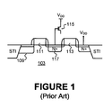
- Figure 1 shows a combination cross-sectional view of a prior art image sensor and active pixel that uses four transistors. This is known in the art as a 4T active pixel.
- the multilayered semiconductor substrate of the present invention can be used with any type of pixel design, including but not limited to 3T, 5T, 6T, and other designs, as well as with CCD or CMOS image sensors..
- Figure 1 shows a cross-section of a four-transistor a pixel 103, which is only one exemplar pixel in the pixel array.
- the pixel includes a photosensitive element 109, which in this embodiment is a pinned photodiode.
- the photosensitive element may be a photogate, photocapacitor, partially pinned photodiode, or unpinned photodiode.
- the term pixel as used herein is meant to encompass all pixel designs, including CCD pixels.
- the photodiode 109 outputs a signal that is used to modulate an amplification transistor 115.
- the amplification transistor 115 is also referred to as a source follower transistor.
- a transfer transistor having a transfer gate 111 is used to transfer the signal output by the photodiode 109 to a floating node 117 (N+ doped) and the gate of the amplification transistor 115.
- the photodiode 109 stores charge (in response to incident light) that is held in the N layer of the photodiode 109.
- the transfer gate 111 is turned on to transfer the charge held in the N- layer to the floating node 117.
- the transfer gate 117 is turned off again for the start of a subsequent integration period.
- the signal on the floating node 117 is then used to modulate the amplification transistor 115.
- a reset transistor having a reset gate 113 resets the floating node 117 to a reference voltage.
- the reference voltage is V dd .
- the present invention uses a multilayered semiconductor substrate (or a single layered silicon-germanium substrate) in order to increase sensitivity in the infrared spectrum.
- a multilayered semiconductor substrate or a single layered silicon-germanium substrate
- particular emphasis is placed upon the particular layers and composition of the semiconductor substrate.
- the steps in the formation of the pixels of the image sensor are not described in detail to avoid obscuring the present invention.
- CMOS and CCD image sensors There are a multitude of various structures and methods used to form CMOS and CCD image sensors and the present invention can be used with each of them.
- the semiconductor substrate is typically either n-type silicon, p-type silicon, or p+ silicon with a surface p-type epitaxial layer.
- the substrate is based on silicon, with dopants that modify the conductivity of the substrate, but do not change its fundamental absorption characteristics.
- a silicon-germanium (SiGe) alloy is used to aid in absorbing near infrared incident photons using the photoelectric effect.
- the energy band gap of silicon is reduced as it is alloyed with germanium, substantially increasing the absorption coefficients, especially at longer wavelengths.
- SiGe alloy would make it difficult to form an oxide of germanium that is stable. Without stable oxide formation, it is difficult to make gate dielectrics so commonly used in CMOS processes.
- the present invention proposes a multilayered structure to take advantage of the properties of silicon and silicon-germanium alloys.
- silicon there is a surface layer of silicon that can be doped for forming transistors, photodiodes, oxides, and diffusions.
- the surface silicon layer should be in the range of thickness from 100 angstroms to 3 microns, and preferably between 500 angstroms and 1 micron.
- the silicon layer is a silicon-germanium layer.
- the buried silicon-germanium layer is very effective in absorbing photons via the photoelectric effect which create electron-hole pairs. These charged particles can be separated through the combination of well known doping profiles and the application of voltage driving forces.
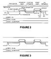
- FIG. 2 For example, turning to Figure 2, there is shown a multilayered semiconductor substrate.
- Figure 2 shows three layers denoted as Layer 1, Layer 2, and Layer 3.
- the bottom most layer, Layer 3, is the base substrate.
- This base substrate may be, as some examples, a p-type substrate, an n-type substrate, or any conventional silicon based substrate.
- Layer 3 may either be a p-type silicon, a p+ silicon substrate, or a p-type epitaxial silicon layer over a p+ silicon substrate.
- Layer 3 may be an n-type silicon, an n+ silicon substrate, or a n-type epitaxial silicon layer over a n+ silicon substrate.
- Layer 2 is a silicon-germanium alloy layer.
- the silicon-germanium alloy layer may be p-type doped.
- the silicon-germanium alloy layer may be n-type doped.
- the silicon-germanium allow may be formed using an epitaxial growth process.
- the SiGe alloy layer (Layer 2) is approximately 1 micron to 20 microns thick.
- the SiGe alloy is doped p-type. This doping can be done insitu during the epitaxial growth or with a subsequent p-type implant.
- the p-type doping concentration in the SiGe alloy may be in the range of 1E14/cm 3 to 1E16/cm 3 , and preferably 3E14/cm 3 to 4E15/cm 3 .
- a silicon layer (Layer 1) formed atop of the silicon-germanium layer is a silicon layer (Layer 1), which may be p-type for pixel arrays using n-channel transistors.
- the silicon layer (Layer 1) may be n-type. Note that the thickness of the silicon layer (Layer 1) is adequate to contain the pixel structures formed on the substrate, including the photodiode, the various N+ and n- doped regions, and the shallow trench isolations (STI) regions.
- the surface silicon layer (Layer 1) may be in the range of 100 A to 3 microns, and preferably 500 A to 1 micron.
- the depletion region of the voltage biased photodiode extends into the SiGe layer and is effective in collecting electrons generated in the SiGe layer.
- the silicon-germanium alloy layer (Layer 1) is formed directly atop of the underlying substrate (Layer 2).
- the top surface is silicon-germanium and not silicon, in contrast to the embodiment shown in Figure 2.
- the structures and doped regions forming the pixel are formed directly in the silicon-germanium layer (Layer 1).
- the silicon-germanium layer (Layer 1) is p-type and the substrate (Layer 2) is also p-type.
- both the silicon-germanium layer (Layer 1) and the substrate (Layer 2) are n-type.
- the concentration of germanium relative to silicon increases with depth, such that there is a relatively low germanium concentration at the surface and a relatively high doping concentration at the bottom of the silicon-germanium layer (Layer 1).
- the SiGe layer While it can be advantageous for the SiGe layer to have a Ge doping gradient, it is also contemplated that a SiGe alloy of a single uniform alloy composition may be used. Still, the doping gradient of germanium may be advantageous in forming an oxide on the surface. By reducing the germanium concentration near the surface, this will enhance oxide formation. However, by using a SiGe alloy with sufficient Ge concentration to provide a useful increase in light absorption and still be able to grow a stable oxide, then a single, uniform SiGe alloy could be realized.
- the SiGe alloy layer (Layer 1 in Fig 3) is approximately 1 micron to 20 micron thick.
- the SiGe alloy is doped p-type. This doping can be done insitu during the epitaxial growth or with a subsequent p-type implant.
- the p-type doping concentration in the SiGe alloy is approximately 1E14/cm 3 to 1E16/cm 3 , and preferably 3E14/cm 3 to 4E15/cm 3 .
- the substrate layer (Layer 2) is formed from silicon-germanium and an epitaxial silicon layer (Layer 1) is grown atop the silicon-germanium substrate.
- the surface silicon layer (Layer 1) may have a thickness in the range of 100 angstroms to 3 microns thick, and preferably between 500 angstroms and 1 micron thick.
- Both the surface silicon layer and the SiGe substrate should be doped p-type for the case of a pixel array formed using n-channel transistors.
- the p-type doping concentration in both the surface silicon layer and the SiGe alloy is approximately 1e14/cm 3 to 1e16/cm 3 , and preferably between 3e14/cm 3 to 4e15/cm 3 .
- the pixel is formed directly onto a silicon-germanium substrate.
- the germanium has a uniform concentration gradient
- the germanium has a concentration gradient where the concentration of germanium at the surface of the silicon-germanium substrate is relatively low compared to that deeper into the substrate. In this embodiment, it is advantageous to have a low germanium doping concentration at the surface.
- the SiGe substrate should be doped p-type for the case of a pixel array formed using n-channel transistors.
- the p-type doping concentration in the SiGe alloy is approximately 1e14/cm 3 to 1e16/cm 3 , and preferably between 3e14/cm 3 to 4e15/cm 3 .
Landscapes
- Solid State Image Pick-Up Elements (AREA)
- Light Receiving Elements (AREA)
- Photometry And Measurement Of Optical Pulse Characteristics (AREA)
Abstract
Description
- The present invention relates to image sensors, and more particularly, to an image sensor formed on a multilayered semiconductor substrate.
- Image sensors have become ubiquitous. They are widely used in digital still cameras, cellular phones, security cameras, medical, automobile, and other applications. The technology used to manufacture image sensors, and in particular CMOS image sensors, has continued to advance at great pace.
- However, current image sensors have very poor sensitivity in the wavelength range of 700 nm to 1000 nm. This wavelength range is loosely referred to as the infrared region of the electromagnetic spectrum. Both CCD and CMOS image sensors suffer from this poor sensitivity. This results from a particular characteristic of silicon semiconductor technology. Specifically, silicon has an energy band gap (EG) of 1.12 eV. Thus, for an electron to be created by the absorption of an incident photon, the photon must have a minimum energy of 1.12 eV to cause an electron in the silicon valence band to be excited to the silicon conduction band. This minimum photon energy is the silicon band gap energy of 1.12 eV. This amount of minimum energy corresponds to a photon wavelength of less than or equal to 1100 nm. Photons having a wavelength of 1100 nm or greater are not absorbed at all and pass through the silicon sensor without being detected.
- Further, as the wavelength of light approaches 1100 nm, the absorption coefficient of the light dramatically decreases so that the sensitivity for detecting photons in the wavelength range of 700 nm to 1100 nm dramatically degrades. The photons are in fact absorbed too deep in the silicon to be detected by the photosensitive element which is typically located near the surface region of the semiconductor substrate. Even at 700 nm the average photon penetration depth is 5 microns below the surface. This is well below the depletion region of the photodiode. So even at 700 nm it is difficult for the photodiode to collect the electrons generated by photons with a wavelength of 700 nm. Longer wavelengths are even more difficult to collect.
- Automotive image sensors are one example of an application requiring improved performance in the infrared spectrum. For example, in one application, passengers are exposed to infrared radiation in the wavelength range of 850 nm to 950 nm. The image sensor is required to see the passengers under this illumination. This allows the location and size of the passengers to be determined even at night when there is no other illumination on the passengers. This information could then be used to determine the conditions for proper airbag deployment in the case of an accident.
- Thus, it would be advantageous to have an image sensor with improved sensitivity in the near infrared wavelengths of 800 nm to 1100 nm.
- In a first aspect, the present invention provides an integrated circuit according to
Claim 1. -
- Figure 1 is a cross-sectional view of a prior art four transistor pixel.
- Figure 2 shows a first embodiment of a multilayered semiconductor substrate formed in accordance with the present invention with a four transistor pixel formed therein.
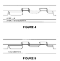
- Figure 3 is a second embodiment of a multilayered semiconductor substrate with a four transistor pixel formed therein.
- Figure 4 is a third embodiment of a multilayered semiconductor substrate with a four transistor pixel formed therein.
- Figure 5 is a fourth embodiment of a multilayered semiconductor substrate with a four transistor pixel formed therein.
- In the following description, numerous specific details are provided in order to give a thorough understanding of embodiments of the invention. One skilled in the relevant art will recognize, however, that the invention may be practiced without one or more of the specific details, or with other methods, components, materials, etc. In other instances, well known structures, materials, or operations are not shown or described in order to avoid obscuring aspects of the invention.
- Reference throughout the specification to "one embodiment" or "an embodiment" means that a particular feature, structure, or characteristic described in connection with the embodiment and included in at least one embodiment of the present invention. Thus, the appearances of the phrase "in one embodiment" or "in an embodiment" in various places throughout the specification are not necessarily all referring to the same embodiment. Furthermore, the particular features, structures, or characteristics may be combined in any suitable manner in one or more embodiments.
- Figure 1 shows a combination cross-sectional view of a prior art image sensor and active pixel that uses four transistors. This is known in the art as a 4T active pixel. However, it can be appreciated that the multilayered semiconductor substrate of the present invention can be used with any type of pixel design, including but not limited to 3T, 5T, 6T, and other designs, as well as with CCD or CMOS image sensors..
- Figure 1 shows a cross-section of a four-transistor a
pixel 103, which is only one exemplar pixel in the pixel array. The pixel includes aphotosensitive element 109, which in this embodiment is a pinned photodiode. However, the photosensitive element may be a photogate, photocapacitor, partially pinned photodiode, or unpinned photodiode. Further, the term pixel as used herein is meant to encompass all pixel designs, including CCD pixels. - The
photodiode 109, outputs a signal that is used to modulate anamplification transistor 115. Theamplification transistor 115 is also referred to as a source follower transistor. A transfer transistor having atransfer gate 111 is used to transfer the signal output by thephotodiode 109 to a floating node 117 (N+ doped) and the gate of theamplification transistor 115. - In operation, during an integration period (also referred to as an exposure or accumulation period), the
photodiode 109 stores charge (in response to incident light) that is held in the N layer of thephotodiode 109. After the integration period, thetransfer gate 111 is turned on to transfer the charge held in the N- layer to thefloating node 117. After the signal has been transferred to thefloating node 117, thetransfer gate 117 is turned off again for the start of a subsequent integration period. The signal on thefloating node 117 is then used to modulate theamplification transistor 115. After readout, a reset transistor having areset gate 113 resets thefloating node 117 to a reference voltage. In one embodiment, the reference voltage is Vdd. - The present invention uses a multilayered semiconductor substrate (or a single layered silicon-germanium substrate) in order to increase sensitivity in the infrared spectrum. In the drawings and description detailed below, particular emphasis is placed upon the particular layers and composition of the semiconductor substrate. The steps in the formation of the pixels of the image sensor are not described in detail to avoid obscuring the present invention. There are a multitude of various structures and methods used to form CMOS and CCD image sensors and the present invention can be used with each of them.
- For a more complete description of image sensor technology, please refer to my copending U.S. Patent Application Serial No. 10/966,137 filed October 15, 2004 entitled "Image Sensor and Pixel that has Positive Transfer Gate Voltage During Integration" and/or U.S. Patent Application Serial No. 11/007,859 filed December 9, 2004 entitled "Local Interconnect Structure and Method for a CMOS Image Sensor," commonly assigned to the assignee of the present invention and herein incorporated by reference in their entireties.
- In current CCD and CMOS image sensors, the semiconductor substrate is typically either n-type silicon, p-type silicon, or p+ silicon with a surface p-type epitaxial layer. In each of these cases, the substrate is based on silicon, with dopants that modify the conductivity of the substrate, but do not change its fundamental absorption characteristics.
- While it is true that a heavily doped p+ silicon substrate will have an increased absorption coefficient due to "free carrier" absorption, this phenomena is not useful in the imaging context because electron-hole pairs are not created. Further, the use of a p+ silicon substrate having an abundance of holes provides very fast recombination that eliminates any generated electrons.
- In accordance with the present invention, a silicon-germanium (SiGe) alloy is used to aid in absorbing near infrared incident photons using the photoelectric effect. The energy band gap of silicon is reduced as it is alloyed with germanium, substantially increasing the absorption coefficients, especially at longer wavelengths. However, it has been recognized that such a SiGe alloy would make it difficult to form an oxide of germanium that is stable. Without stable oxide formation, it is difficult to make gate dielectrics so commonly used in CMOS processes.
- Because the absorption coefficient at shorter wavelengths (i.e., the visible spectrum) is not an issue for an infrared sensor, the present invention, in one embodiment, proposes a multilayered structure to take advantage of the properties of silicon and silicon-germanium alloys. In particular, as detailed below, there is a surface layer of silicon that can be doped for forming transistors, photodiodes, oxides, and diffusions. The surface silicon layer should be in the range of thickness from 100 angstroms to 3 microns, and preferably between 500 angstroms and 1 micron. By using a SiGe alloy, the absorption at all wavelengths is increased and the absorption coefficients in the visible spectrum are also increased. Since the electrons are generated closer to the surface and closer to the photodiode, there is less chance for the generated electron to diffuse to the adjacent pixel's photodiode. This improves crosstalk at all wavelengths, which is a benefit for both visible and IR sensors. Thus, while this invention is of particular benefit to IR sensors, the teachings of the present invention may also be used advantageously for sensors designed to operate in the visible spectrum.
- Underneath the silicon layer is a silicon-germanium layer. In the light sensitive area, e.g. the photodiode region, the buried silicon-germanium layer is very effective in absorbing photons via the photoelectric effect which create electron-hole pairs. These charged particles can be separated through the combination of well known doping profiles and the application of voltage driving forces.
- For example, turning to Figure 2, there is shown a multilayered semiconductor substrate. Figure 2 shows three layers denoted as
Layer 1,Layer 2, andLayer 3. The bottom most layer,Layer 3, is the base substrate. This base substrate may be, as some examples, a p-type substrate, an n-type substrate, or any conventional silicon based substrate. - As further examples, for pixel arrays that use n-channel transistors,
Layer 3 may either be a p-type silicon, a p+ silicon substrate, or a p-type epitaxial silicon layer over a p+ silicon substrate. For pixel arrays that use p-channel transistors,Layer 3 may be an n-type silicon, an n+ silicon substrate, or a n-type epitaxial silicon layer over a n+ silicon substrate. -
Layer 2 is a silicon-germanium alloy layer. For pixel arrays that use n-channel transistors, the silicon-germanium alloy layer may be p-type doped. For pixel arrays that use p-channel transistors, the silicon-germanium alloy layer may be n-type doped. The silicon-germanium allow may be formed using an epitaxial growth process. In one embodiment, the SiGe alloy layer (Layer 2) is approximately 1 micron to 20 microns thick. For the aforementioned case of pixel arrays that use n-channel transistors, the SiGe alloy is doped p-type. This doping can be done insitu during the epitaxial growth or with a subsequent p-type implant. The p-type doping concentration in the SiGe alloy may be in the range of 1E14/cm3 to 1E16/cm3, and preferably 3E14/cm3 to 4E15/cm3. - Finally, formed atop of the silicon-germanium layer is a silicon layer (Layer 1), which may be p-type for pixel arrays using n-channel transistors. For pixel arrays using p-channel transistors, the silicon layer (Layer 1) may be n-type. Note that the thickness of the silicon layer (Layer 1) is adequate to contain the pixel structures formed on the substrate, including the photodiode, the various N+ and n- doped regions, and the shallow trench isolations (STI) regions. The surface silicon layer (Layer 1) may be in the range of 100 A to 3 microns, and preferably 500 A to 1 micron. The depletion region of the voltage biased photodiode extends into the SiGe layer and is effective in collecting electrons generated in the SiGe layer.
- Turning to Figure 3, in an alternative embodiment, the silicon-germanium alloy layer (Layer 1) is formed directly atop of the underlying substrate (Layer 2). The top surface is silicon-germanium and not silicon, in contrast to the embodiment shown in Figure 2. Thus, the structures and doped regions forming the pixel are formed directly in the silicon-germanium layer (Layer 1). For pixel arrays that use n-channel transistors, the silicon-germanium layer (Layer 1) is p-type and the substrate (Layer 2) is also p-type. For pixel arrays using p-channel transistors, both the silicon-germanium layer (Layer 1) and the substrate (Layer 2) are n-type. In this embodiment, where the surface layer is silicon-germanium, the concentration of germanium relative to silicon increases with depth, such that there is a relatively low germanium concentration at the surface and a relatively high doping concentration at the bottom of the silicon-germanium layer (Layer 1).
- While it can be advantageous for the SiGe layer to have a Ge doping gradient, it is also contemplated that a SiGe alloy of a single uniform alloy composition may be used. Still, the doping gradient of germanium may be advantageous in forming an oxide on the surface. By reducing the germanium concentration near the surface, this will enhance oxide formation. However, by using a SiGe alloy with sufficient Ge concentration to provide a useful increase in light absorption and still be able to grow a stable oxide, then a single, uniform SiGe alloy could be realized.
- The SiGe alloy layer (
Layer 1 in Fig 3) is approximately 1 micron to 20 micron thick. For the aforementioned case of pixel arrays that use n-channel transistors the SiGe alloy is doped p-type. This doping can be done insitu during the epitaxial growth or with a subsequent p-type implant. The p-type doping concentration in the SiGe alloy is approximately 1E14/cm3 to 1E16/cm3, and preferably 3E14/cm3 to 4E15/cm3. - Turning to Figure 4, in a third embodiment, the substrate layer (Layer 2) is formed from silicon-germanium and an epitaxial silicon layer (Layer 1) is grown atop the silicon-germanium substrate. This embodiment is similar to that of Figure 2 except that the silicon-germanium layer is also used as the substrate. The surface silicon layer (Layer 1) may have a thickness in the range of 100 angstroms to 3 microns thick, and preferably between 500 angstroms and 1 micron thick. Both the surface silicon layer and the SiGe substrate should be doped p-type for the case of a pixel array formed using n-channel transistors. The p-type doping concentration in both the surface silicon layer and the SiGe alloy is approximately 1e14/cm3 to 1e16/cm3, and preferably between 3e14/cm3 to 4e15/cm3.
- Further, in yet another alternative embodiment, as seen in Figure 5, the pixel is formed directly onto a silicon-germanium substrate. While in one embodiment, the germanium has a uniform concentration gradient, in alternative embodiments, the germanium has a concentration gradient where the concentration of germanium at the surface of the silicon-germanium substrate is relatively low compared to that deeper into the substrate. In this embodiment, it is advantageous to have a low germanium doping concentration at the surface. The SiGe substrate should be doped p-type for the case of a pixel array formed using n-channel transistors. The p-type doping concentration in the SiGe alloy is approximately 1e14/cm3 to 1e16/cm3, and preferably between 3e14/cm3 to 4e15/cm3 .
- Thus, from the foregoing, it will be appreciated that specific embodiments of the invention have been described herein for purposes of illustration, but that various modifications may be made without deviating from the spirit and scope of the invention. Accordingly, the invention is not limited except as by the appended claims.
Claims (13)
- An integrated circuit comprising:a multilayered semiconductor structure, said multilayered semiconductor structure formed from a silicon-germanium alloy layer formed over a silicon substrate; anda pixel formed in said silicon-germanium alloy layer.
- The integrated circuit of Claim 1 wherein said pixel includes a photosensitive element selected from the group of: a photodiode, partially pinned photodiode, pinned photodiode, photogate, or photocapacitor.
- The integrated circuit of Claim 1 wherein said multilayered semiconductor substrate further includes a silicon top layer formed over said silicon-germanium alloy layer and said pixel is formed in said silicon top layer.
- The integrated circuit of Claim 1 wherein said silicon-germanium alloy layer has a thickness of between 1 micron to 20 microns.
- The integrated circuit of Claim 3 wherein said silicon top layer has a thickness of between 100 angstroms to 3 microns.
- The integrated circuit of Claim 1 wherein said silicon-germanium alloy layer has a germanium concentration gradient such that an upper portion of said silicon-germanium alloy layer has a lower germanium concentration than a lower portion of said silicon-germanium alloy layer.
- An integrated circuit comprising:a silicon-germanium alloy substrate; anda pixel formed in said silicon-germanium alloy layer.
- The integrated circuit of Claim 7 wherein said pixel includes a photosensitive element selected from the group of: a photodiode, partially pinned photodiode, pinned photodiode, photogate, or photocapacitor.
- The integrated circuit of Claim 7 further including a silicon top layer formed over said silicon-germanium alloy substrate and said pixel is formed in said silicon top layer.
- The integrated circuit of Claim 9 wherein said silicon top layer has a thickness of between 100 angstroms to 3 microns.
- The integrated circuit of Claim 7 wherein said silicon-germanium alloy substrate has a germanium concentration gradient such that an upper portion of said silicon-germanium alloy substrate has a lower germanium concentration than a lower portion of said silicon-germanium alloy substrate.
- The integrated circuit of Claim 9 wherein said silicon-germanium alloy substrate has a germanium concentration gradient such that an upper portion of said silicon-germanium alloy substrate has a lower germanium concentration than a lower portion of said silicon-germanium alloy substrate.
- The integrated circuit of Claim 7 wherein said silicon-germanium alloy substrate has a uniform germanium concentration.
Applications Claiming Priority (1)
| Application Number | Priority Date | Filing Date | Title |
|---|---|---|---|
| US11/038,594 US20060157806A1 (en) | 2005-01-18 | 2005-01-18 | Multilayered semiconductor susbtrate and image sensor formed thereon for improved infrared response |
Publications (3)
| Publication Number | Publication Date |
|---|---|
| EP1681722A2 true EP1681722A2 (en) | 2006-07-19 |
| EP1681722A3 EP1681722A3 (en) | 2007-05-30 |
| EP1681722B1 EP1681722B1 (en) | 2011-09-28 |
Family
ID=36061375
Family Applications (1)
| Application Number | Title | Priority Date | Filing Date |
|---|---|---|---|
| EP05257881A Expired - Lifetime EP1681722B1 (en) | 2005-01-18 | 2005-12-20 | Multilayered semiconductor substrate and image sensor formed thereon for improved infrared response |
Country Status (5)
| Country | Link |
|---|---|
| US (1) | US20060157806A1 (en) |
| EP (1) | EP1681722B1 (en) |
| CN (1) | CN1828917B (en) |
| AT (1) | ATE526685T1 (en) |
| TW (1) | TWI305414B (en) |
Families Citing this family (26)
| Publication number | Priority date | Publication date | Assignee | Title |
|---|---|---|---|---|
| KR100625944B1 (en) * | 2005-06-30 | 2006-09-18 | 매그나칩 반도체 유한회사 | Photodiode of CMOS image sensor and its manufacturing method |
| JP4984634B2 (en) * | 2005-07-21 | 2012-07-25 | ソニー株式会社 | Physical information acquisition method and physical information acquisition device |
| US7943471B1 (en) * | 2006-05-15 | 2011-05-17 | Globalfoundries Inc. | Diode with asymmetric silicon germanium anode |
| EP2064746A2 (en) | 2006-09-29 | 2009-06-03 | University of Florida Research Foundation, Incorporated | Method and apparatus for infrared detection and display |
| US7825465B2 (en) * | 2007-12-13 | 2010-11-02 | Fairchild Semiconductor Corporation | Structure and method for forming field effect transistor with low resistance channel region |
| CN101459184B (en) * | 2007-12-13 | 2011-03-23 | 中芯国际集成电路制造(上海)有限公司 | System and method for sensing image on CMOS |
| CN100595934C (en) * | 2008-01-23 | 2010-03-24 | 厦门大学 | Silicon-germanium heterojunction phototransistor based on virtual substrate |
| US10636929B2 (en) | 2009-04-30 | 2020-04-28 | Massachusetts Institute Of Technology | Cross-talk suppression in Geiger-mode avalanche photodiodes |
| US20110169991A1 (en) * | 2010-01-08 | 2011-07-14 | Omnivision Technologies, Inc. | Image sensor with epitaxially self-aligned photo sensors |
| JP5778261B2 (en) | 2010-05-24 | 2015-09-16 | ユニバーシティ オブ フロリダ リサーチ ファウンデーション,インク.University Of Florida Reseatch Foundation,Inc. | Method and apparatus for providing a charge blocking layer on an infrared upconversion device |
| RU2014102650A (en) | 2011-06-30 | 2015-08-10 | Юниверсити Оф Флорида Рисеч Фаундэйшн, Инк. | REINFORCING INFRARED PHOTODETECTOR AND ITS APPLICATION FOR DETECTING IR RADIATION |
| JP2013157367A (en) * | 2012-01-27 | 2013-08-15 | Sony Corp | Image sensor, production apparatus and method, and imaging apparatus |
| WO2014178923A2 (en) * | 2013-01-25 | 2014-11-06 | University Of Florida Research Foundation, Inc. | A novel ir image sensor using a solution processed pbs photodetector |
| CN104078472B (en) * | 2013-03-27 | 2017-02-01 | 中芯国际集成电路制造(上海)有限公司 | CMOS (Complementary Metal Oxide Semiconductor) image sensor and manufacturing method thereof |
| US9153717B2 (en) | 2013-08-09 | 2015-10-06 | Taiwan Semiconductor Manufacturing Company, Ltd. | Backside illuminated photo-sensitive device with gradated buffer layer |
| JP6302216B2 (en) * | 2013-11-08 | 2018-03-28 | ルネサスエレクトロニクス株式会社 | Semiconductor device and manufacturing method thereof |
| US9806122B2 (en) | 2014-07-25 | 2017-10-31 | Omnivision Technologies, Inc. | Visible and infrared image sensor |
| KR20170077241A (en) | 2014-11-13 | 2017-07-05 | 아티룩스 인코포레이티드 | Light absorption apparatus |
| US9799689B2 (en) | 2014-11-13 | 2017-10-24 | Artilux Inc. | Light absorption apparatus |
| JP2016126472A (en) * | 2014-12-26 | 2016-07-11 | 株式会社東芝 | Cardiac rate detecting device, and face recognition system using the same |
| CA2988784A1 (en) | 2015-06-11 | 2017-03-09 | University Of Florida Research Foundation, Incorporated | Monodisperse, ir-absorbing nanoparticles and related methods and devices |
| US9859325B2 (en) * | 2015-11-13 | 2018-01-02 | Taiwan Semiconductor Manufacturing Co., Ltd. | Complementary metal-oxide-semiconductor (CMOS) image sensor with silicon and silicon germanium |
| FR3111019B1 (en) * | 2020-05-26 | 2022-07-22 | St Microelectronics Crolles 2 Sas | Integrated optical sensor with pinched photodiodes |
| CN113725242B (en) * | 2020-05-26 | 2025-04-25 | 意法半导体(克洛尔2)公司 | Integrated optical sensor with pinned photodiode |
| US20220252725A1 (en) * | 2021-02-05 | 2022-08-11 | Artilux, Inc. | Lidar Sensor with Dynamic Projection Patterns |
| EP4496010B1 (en) * | 2022-03-16 | 2026-05-06 | Optohub Co., Ltd | Light detection device |
Citations (2)
| Publication number | Priority date | Publication date | Assignee | Title |
|---|---|---|---|---|
| EP0515859A1 (en) | 1991-05-31 | 1992-12-02 | International Business Machines Corporation | Low defect density/arbitrary lattice constant hetero-epitaxial layers |
| US20050006565A1 (en) | 2003-07-07 | 2005-01-13 | Chandra Mouli | Pixel with strained silicon layer for improving carrier mobility and blue response in imagers |
Family Cites Families (10)
| Publication number | Priority date | Publication date | Assignee | Title |
|---|---|---|---|---|
| US4758734A (en) * | 1984-03-13 | 1988-07-19 | Nec Corporation | High resolution image sensor array using amorphous photo-diodes |
| US6403975B1 (en) * | 1996-04-09 | 2002-06-11 | Max-Planck Gesellschaft Zur Forderung Der Wissenschafteneev | Semiconductor components, in particular photodetectors, light emitting diodes, optical modulators and waveguides with multilayer structures grown on silicon substrates |
| KR19990023221A (en) * | 1997-08-20 | 1999-03-25 | 포만 제프리 엘 | Photosensitive Device, Active Pixel Sensor Device, Active Pixel Sensor Photosensitive Device, and Active Pixel Sensor Device |
| JP4376516B2 (en) * | 2000-10-19 | 2009-12-02 | クォンタム セミコンダクター リミテッド ライアビリティ カンパニー | Method for manufacturing heterojunction photodiode integrated with CMOS |
| EP1415331A2 (en) * | 2001-08-06 | 2004-05-06 | Massachusetts Institute Of Technology | Formation of planar strained layers |
| US6980748B2 (en) * | 2001-08-30 | 2005-12-27 | International Business Machines Corporation | SiGe or germanium flip chip optical receiver |
| GB0216075D0 (en) * | 2002-07-11 | 2002-08-21 | Qinetiq Ltd | Photodetector circuits |
| US6919552B2 (en) * | 2002-11-25 | 2005-07-19 | Agilent Technologies, Inc. | Optical detector and method for detecting incident light |
| US6921934B2 (en) * | 2003-03-28 | 2005-07-26 | Micron Technology, Inc. | Double pinned photodiode for CMOS APS and method of formation |
| US7122392B2 (en) * | 2003-06-30 | 2006-10-17 | Intel Corporation | Methods of forming a high germanium concentration silicon germanium alloy by epitaxial lateral overgrowth and structures formed thereby |
-
2005
- 2005-01-18 US US11/038,594 patent/US20060157806A1/en not_active Abandoned
- 2005-12-20 AT AT05257881T patent/ATE526685T1/en not_active IP Right Cessation
- 2005-12-20 EP EP05257881A patent/EP1681722B1/en not_active Expired - Lifetime
- 2005-12-28 TW TW094143731A patent/TWI305414B/en not_active IP Right Cessation
-
2006
- 2006-01-18 CN CN200610005998XA patent/CN1828917B/en not_active Expired - Lifetime
Patent Citations (2)
| Publication number | Priority date | Publication date | Assignee | Title |
|---|---|---|---|---|
| EP0515859A1 (en) | 1991-05-31 | 1992-12-02 | International Business Machines Corporation | Low defect density/arbitrary lattice constant hetero-epitaxial layers |
| US20050006565A1 (en) | 2003-07-07 | 2005-01-13 | Chandra Mouli | Pixel with strained silicon layer for improving carrier mobility and blue response in imagers |
Also Published As
| Publication number | Publication date |
|---|---|
| US20060157806A1 (en) | 2006-07-20 |
| TW200627635A (en) | 2006-08-01 |
| CN1828917A (en) | 2006-09-06 |
| EP1681722A3 (en) | 2007-05-30 |
| TWI305414B (en) | 2009-01-11 |
| EP1681722B1 (en) | 2011-09-28 |
| CN1828917B (en) | 2012-11-21 |
| ATE526685T1 (en) | 2011-10-15 |
Similar Documents
| Publication | Publication Date | Title |
|---|---|---|
| EP1681722B1 (en) | Multilayered semiconductor substrate and image sensor formed thereon for improved infrared response | |
| US8389319B2 (en) | SOI-based CMOS imagers employing flash gate/chemisorption processing | |
| USRE45357E1 (en) | Twin p-well CMOS imager | |
| US11973093B2 (en) | Visible-to-longwave infrared single photon avalanche photodetector on silicon | |
| EP2244296B1 (en) | Multilayer image sensor pixel structure for reducing crosstalk | |
| JP5295105B2 (en) | Low crosstalk PMOS pixel structure | |
| US7939357B2 (en) | Image sensor pixel having photodiode with multi-dopant implantation | |
| US7608874B2 (en) | Fully isolated photodiode stack | |
| US20040262622A1 (en) | Double pinned photodiode for CMOS APS and method of formation | |
| US20050205930A1 (en) | Silicon-on-insulator active pixel sensors | |
| JP2004512686A (en) | Method of manufacturing heterojunction photodiode integrated with CMOS | |
| JPH11317512A (en) | CMOS image sensor and method of manufacturing the same | |
| US20090127643A1 (en) | Photodiode of an image sensor and fabricating method thereof | |
| US20080318358A1 (en) | Image sensor pixel having photodiode with indium pinning layer | |
| US7304338B2 (en) | Solid-state image sensor and method for fabricating the same | |
| US11676987B2 (en) | Semiconductor structure and the manufacturing method thereof | |
| US20120104464A1 (en) | P-pixel cmos imagers using ultra-thin silicon on insulator substrates (utsoi) | |
| US20010019851A1 (en) | Reduced leakage trench isolation | |
| TWI426603B (en) | Hole-based ultra-deep photodiode in a cmos image sensor and a process thereof | |
| KR100326267B1 (en) | Image sensor and method for fabricating the same | |
| US20060124929A1 (en) | Semiconductor substrate for solid-state image pickup device and producing method therefor | |
| Augusto et al. | A new CMOS SiGeC avalanche photo-diode pixel for IR sensing |
Legal Events
| Date | Code | Title | Description |
|---|---|---|---|
| PUAI | Public reference made under article 153(3) epc to a published international application that has entered the european phase |
Free format text: ORIGINAL CODE: 0009012 |
|
| 17P | Request for examination filed |
Effective date: 20060109 |
|
| AK | Designated contracting states |
Kind code of ref document: A2 Designated state(s): AT BE BG CH CY CZ DE DK EE ES FI FR GB GR HU IE IS IT LI LT LU LV MC NL PL PT RO SE SI SK TR |
|
| AX | Request for extension of the european patent |
Extension state: AL BA HR MK YU |
|
| PUAL | Search report despatched |
Free format text: ORIGINAL CODE: 0009013 |
|
| AK | Designated contracting states |
Kind code of ref document: A3 Designated state(s): AT BE BG CH CY CZ DE DK EE ES FI FR GB GR HU IE IS IT LI LT LU LV MC NL PL PT RO SE SI SK TR |
|
| AX | Request for extension of the european patent |
Extension state: AL BA HR MK YU |
|
| 17Q | First examination report despatched |
Effective date: 20071010 |
|
| AKX | Designation fees paid |
Designated state(s): AT BE BG CH CY CZ DE DK EE ES FI FR GB GR HU IE IS IT LI LT LU LV MC NL PL PT RO SE SI SK TR |
|
| GRAP | Despatch of communication of intention to grant a patent |
Free format text: ORIGINAL CODE: EPIDOSNIGR1 |
|
| GRAS | Grant fee paid |
Free format text: ORIGINAL CODE: EPIDOSNIGR3 |
|
| GRAA | (expected) grant |
Free format text: ORIGINAL CODE: 0009210 |
|
| AK | Designated contracting states |
Kind code of ref document: B1 Designated state(s): AT BE BG CH CY CZ DE DK EE ES FI FR GB GR HU IE IS IT LI LT LU LV MC NL PL PT RO SE SI SK TR |
|
| REG | Reference to a national code |
Ref country code: GB Ref legal event code: FG4D |
|
| REG | Reference to a national code |
Ref country code: CH Ref legal event code: EP |
|
| REG | Reference to a national code |
Ref country code: IE Ref legal event code: FG4D |
|
| REG | Reference to a national code |
Ref country code: DE Ref legal event code: R096 Ref document number: 602005030217 Country of ref document: DE Effective date: 20111201 |
|
| REG | Reference to a national code |
Ref country code: NL Ref legal event code: VDEP Effective date: 20110928 |
|
| PG25 | Lapsed in a contracting state [announced via postgrant information from national office to epo] |
Ref country code: FI Free format text: LAPSE BECAUSE OF FAILURE TO SUBMIT A TRANSLATION OF THE DESCRIPTION OR TO PAY THE FEE WITHIN THE PRESCRIBED TIME-LIMIT Effective date: 20110928 Ref country code: SE Free format text: LAPSE BECAUSE OF FAILURE TO SUBMIT A TRANSLATION OF THE DESCRIPTION OR TO PAY THE FEE WITHIN THE PRESCRIBED TIME-LIMIT Effective date: 20110928 Ref country code: LT Free format text: LAPSE BECAUSE OF FAILURE TO SUBMIT A TRANSLATION OF THE DESCRIPTION OR TO PAY THE FEE WITHIN THE PRESCRIBED TIME-LIMIT Effective date: 20110928 |
|
| LTIE | Lt: invalidation of european patent or patent extension |
Effective date: 20110928 |
|
| PG25 | Lapsed in a contracting state [announced via postgrant information from national office to epo] |
Ref country code: SI Free format text: LAPSE BECAUSE OF FAILURE TO SUBMIT A TRANSLATION OF THE DESCRIPTION OR TO PAY THE FEE WITHIN THE PRESCRIBED TIME-LIMIT Effective date: 20110928 Ref country code: LV Free format text: LAPSE BECAUSE OF FAILURE TO SUBMIT A TRANSLATION OF THE DESCRIPTION OR TO PAY THE FEE WITHIN THE PRESCRIBED TIME-LIMIT Effective date: 20110928 Ref country code: CY Free format text: LAPSE BECAUSE OF FAILURE TO SUBMIT A TRANSLATION OF THE DESCRIPTION OR TO PAY THE FEE WITHIN THE PRESCRIBED TIME-LIMIT Effective date: 20110928 Ref country code: AT Free format text: LAPSE BECAUSE OF FAILURE TO SUBMIT A TRANSLATION OF THE DESCRIPTION OR TO PAY THE FEE WITHIN THE PRESCRIBED TIME-LIMIT Effective date: 20110928 Ref country code: GR Free format text: LAPSE BECAUSE OF FAILURE TO SUBMIT A TRANSLATION OF THE DESCRIPTION OR TO PAY THE FEE WITHIN THE PRESCRIBED TIME-LIMIT Effective date: 20111229 |
|
| REG | Reference to a national code |
Ref country code: AT Ref legal event code: MK05 Ref document number: 526685 Country of ref document: AT Kind code of ref document: T Effective date: 20110928 |
|
| PG25 | Lapsed in a contracting state [announced via postgrant information from national office to epo] |
Ref country code: BE Free format text: LAPSE BECAUSE OF FAILURE TO SUBMIT A TRANSLATION OF THE DESCRIPTION OR TO PAY THE FEE WITHIN THE PRESCRIBED TIME-LIMIT Effective date: 20110928 |
|
| PG25 | Lapsed in a contracting state [announced via postgrant information from national office to epo] |
Ref country code: CZ Free format text: LAPSE BECAUSE OF FAILURE TO SUBMIT A TRANSLATION OF THE DESCRIPTION OR TO PAY THE FEE WITHIN THE PRESCRIBED TIME-LIMIT Effective date: 20110928 Ref country code: IS Free format text: LAPSE BECAUSE OF FAILURE TO SUBMIT A TRANSLATION OF THE DESCRIPTION OR TO PAY THE FEE WITHIN THE PRESCRIBED TIME-LIMIT Effective date: 20120128 Ref country code: SK Free format text: LAPSE BECAUSE OF FAILURE TO SUBMIT A TRANSLATION OF THE DESCRIPTION OR TO PAY THE FEE WITHIN THE PRESCRIBED TIME-LIMIT Effective date: 20110928 |
|
| PG25 | Lapsed in a contracting state [announced via postgrant information from national office to epo] |
Ref country code: RO Free format text: LAPSE BECAUSE OF FAILURE TO SUBMIT A TRANSLATION OF THE DESCRIPTION OR TO PAY THE FEE WITHIN THE PRESCRIBED TIME-LIMIT Effective date: 20110928 Ref country code: PT Free format text: LAPSE BECAUSE OF FAILURE TO SUBMIT A TRANSLATION OF THE DESCRIPTION OR TO PAY THE FEE WITHIN THE PRESCRIBED TIME-LIMIT Effective date: 20120130 Ref country code: NL Free format text: LAPSE BECAUSE OF FAILURE TO SUBMIT A TRANSLATION OF THE DESCRIPTION OR TO PAY THE FEE WITHIN THE PRESCRIBED TIME-LIMIT Effective date: 20110928 Ref country code: IT Free format text: LAPSE BECAUSE OF FAILURE TO SUBMIT A TRANSLATION OF THE DESCRIPTION OR TO PAY THE FEE WITHIN THE PRESCRIBED TIME-LIMIT Effective date: 20110928 Ref country code: EE Free format text: LAPSE BECAUSE OF FAILURE TO SUBMIT A TRANSLATION OF THE DESCRIPTION OR TO PAY THE FEE WITHIN THE PRESCRIBED TIME-LIMIT Effective date: 20110928 |
|
| PG25 | Lapsed in a contracting state [announced via postgrant information from national office to epo] |
Ref country code: DK Free format text: LAPSE BECAUSE OF FAILURE TO SUBMIT A TRANSLATION OF THE DESCRIPTION OR TO PAY THE FEE WITHIN THE PRESCRIBED TIME-LIMIT Effective date: 20110928 Ref country code: MC Free format text: LAPSE BECAUSE OF NON-PAYMENT OF DUE FEES Effective date: 20111231 |
|
| REG | Reference to a national code |
Ref country code: CH Ref legal event code: PL |
|
| PLBE | No opposition filed within time limit |
Free format text: ORIGINAL CODE: 0009261 |
|
| STAA | Information on the status of an ep patent application or granted ep patent |
Free format text: STATUS: NO OPPOSITION FILED WITHIN TIME LIMIT |
|
| PG25 | Lapsed in a contracting state [announced via postgrant information from national office to epo] |
Ref country code: PL Free format text: LAPSE BECAUSE OF FAILURE TO SUBMIT A TRANSLATION OF THE DESCRIPTION OR TO PAY THE FEE WITHIN THE PRESCRIBED TIME-LIMIT Effective date: 20110928 |
|
| 26N | No opposition filed |
Effective date: 20120629 |
|
| REG | Reference to a national code |
Ref country code: IE Ref legal event code: MM4A |
|
| REG | Reference to a national code |
Ref country code: DE Ref legal event code: R097 Ref document number: 602005030217 Country of ref document: DE Effective date: 20120629 |
|
| PG25 | Lapsed in a contracting state [announced via postgrant information from national office to epo] |
Ref country code: CH Free format text: LAPSE BECAUSE OF NON-PAYMENT OF DUE FEES Effective date: 20111231 Ref country code: IE Free format text: LAPSE BECAUSE OF NON-PAYMENT OF DUE FEES Effective date: 20111220 Ref country code: LI Free format text: LAPSE BECAUSE OF NON-PAYMENT OF DUE FEES Effective date: 20111231 |
|
| PG25 | Lapsed in a contracting state [announced via postgrant information from national office to epo] |
Ref country code: ES Free format text: LAPSE BECAUSE OF FAILURE TO SUBMIT A TRANSLATION OF THE DESCRIPTION OR TO PAY THE FEE WITHIN THE PRESCRIBED TIME-LIMIT Effective date: 20120108 |
|
| PG25 | Lapsed in a contracting state [announced via postgrant information from national office to epo] |
Ref country code: LU Free format text: LAPSE BECAUSE OF NON-PAYMENT OF DUE FEES Effective date: 20111220 |
|
| PG25 | Lapsed in a contracting state [announced via postgrant information from national office to epo] |
Ref country code: BG Free format text: LAPSE BECAUSE OF FAILURE TO SUBMIT A TRANSLATION OF THE DESCRIPTION OR TO PAY THE FEE WITHIN THE PRESCRIBED TIME-LIMIT Effective date: 20111228 |
|
| PG25 | Lapsed in a contracting state [announced via postgrant information from national office to epo] |
Ref country code: TR Free format text: LAPSE BECAUSE OF FAILURE TO SUBMIT A TRANSLATION OF THE DESCRIPTION OR TO PAY THE FEE WITHIN THE PRESCRIBED TIME-LIMIT Effective date: 20110928 |
|
| PG25 | Lapsed in a contracting state [announced via postgrant information from national office to epo] |
Ref country code: HU Free format text: LAPSE BECAUSE OF FAILURE TO SUBMIT A TRANSLATION OF THE DESCRIPTION OR TO PAY THE FEE WITHIN THE PRESCRIBED TIME-LIMIT Effective date: 20110928 |
|
| REG | Reference to a national code |
Ref country code: FR Ref legal event code: PLFP Year of fee payment: 11 |
|
| REG | Reference to a national code |
Ref country code: FR Ref legal event code: PLFP Year of fee payment: 12 |
|
| REG | Reference to a national code |
Ref country code: FR Ref legal event code: PLFP Year of fee payment: 13 |
|
| REG | Reference to a national code |
Ref country code: DE Ref legal event code: R079 Ref document number: 602005030217 Country of ref document: DE Free format text: PREVIOUS MAIN CLASS: H01L0027146000 Ipc: H10F0039180000 |
|
| PGFP | Annual fee paid to national office [announced via postgrant information from national office to epo] |
Ref country code: DE Payment date: 20241111 Year of fee payment: 20 |
|
| PGFP | Annual fee paid to national office [announced via postgrant information from national office to epo] |
Ref country code: GB Payment date: 20241114 Year of fee payment: 20 |
|
| PGFP | Annual fee paid to national office [announced via postgrant information from national office to epo] |
Ref country code: FR Payment date: 20241111 Year of fee payment: 20 |
|
| REG | Reference to a national code |
Ref country code: DE Ref legal event code: R071 Ref document number: 602005030217 Country of ref document: DE |
|
| REG | Reference to a national code |
Ref country code: GB Ref legal event code: PE20 Expiry date: 20251219 |