KR20170077241A - Light absorption apparatus - Google Patents
Light absorption apparatus Download PDFInfo
- Publication number
- KR20170077241A KR20170077241A KR1020177015424A KR20177015424A KR20170077241A KR 20170077241 A KR20170077241 A KR 20170077241A KR 1020177015424 A KR1020177015424 A KR 1020177015424A KR 20177015424 A KR20177015424 A KR 20177015424A KR 20170077241 A KR20170077241 A KR 20170077241A
- Authority
- KR
- South Korea
- Prior art keywords
- layer
- light absorbing
- forming
- absorbing device
- region
- Prior art date
Links
- 230000031700 light absorption Effects 0.000 title description 4
- 239000000758 substrate Substances 0.000 claims abstract description 97
- 229910052710 silicon Inorganic materials 0.000 claims abstract description 38
- 125000006850 spacer group Chemical group 0.000 claims abstract description 30
- XUIMIQQOPSSXEZ-UHFFFAOYSA-N Silicon Chemical compound [Si] XUIMIQQOPSSXEZ-UHFFFAOYSA-N 0.000 claims abstract description 26
- 239000010703 silicon Substances 0.000 claims abstract description 26
- 238000002955 isolation Methods 0.000 claims abstract description 23
- 238000000034 method Methods 0.000 claims description 99
- 238000002161 passivation Methods 0.000 claims description 62
- 239000000463 material Substances 0.000 claims description 55
- 239000002019 doping agent Substances 0.000 claims description 52
- 229910052732 germanium Inorganic materials 0.000 claims description 29
- 150000004767 nitrides Chemical class 0.000 claims description 16
- 230000003287 optical effect Effects 0.000 claims description 15
- GNPVGFCGXDBREM-UHFFFAOYSA-N germanium atom Chemical compound [Ge] GNPVGFCGXDBREM-UHFFFAOYSA-N 0.000 claims description 14
- 238000010521 absorption reaction Methods 0.000 claims description 10
- 238000000151 deposition Methods 0.000 claims description 9
- 239000006096 absorbing agent Substances 0.000 claims description 8
- 238000002310 reflectometry Methods 0.000 claims description 5
- 229910021332 silicide Inorganic materials 0.000 claims description 5
- FVBUAEGBCNSCDD-UHFFFAOYSA-N silicide(4-) Chemical compound [Si-4] FVBUAEGBCNSCDD-UHFFFAOYSA-N 0.000 claims description 5
- 230000035945 sensitivity Effects 0.000 claims description 2
- 230000002745 absorbent Effects 0.000 claims 1
- 239000002250 absorbent Substances 0.000 claims 1
- 239000010410 layer Substances 0.000 description 446
- 230000008569 process Effects 0.000 description 60
- 239000004065 semiconductor Substances 0.000 description 36
- 238000009792 diffusion process Methods 0.000 description 27
- 230000012010 growth Effects 0.000 description 22
- 229910000577 Silicon-germanium Inorganic materials 0.000 description 19
- 238000005530 etching Methods 0.000 description 16
- 238000004519 manufacturing process Methods 0.000 description 13
- 238000005498 polishing Methods 0.000 description 11
- VYPSYNLAJGMNEJ-UHFFFAOYSA-N silicon dioxide Inorganic materials O=[Si]=O VYPSYNLAJGMNEJ-UHFFFAOYSA-N 0.000 description 9
- 238000013459 approach Methods 0.000 description 8
- 230000007547 defect Effects 0.000 description 8
- 230000015572 biosynthetic process Effects 0.000 description 7
- 229910052751 metal Inorganic materials 0.000 description 7
- 239000002184 metal Substances 0.000 description 7
- 238000005468 ion implantation Methods 0.000 description 6
- 239000000203 mixture Substances 0.000 description 6
- 238000001020 plasma etching Methods 0.000 description 6
- 230000008021 deposition Effects 0.000 description 5
- NBIIXXVUZAFLBC-UHFFFAOYSA-N Phosphoric acid Chemical compound OP(O)(O)=O NBIIXXVUZAFLBC-UHFFFAOYSA-N 0.000 description 4
- 238000010586 diagram Methods 0.000 description 4
- 238000011065 in-situ storage Methods 0.000 description 4
- 239000011229 interlayer Substances 0.000 description 4
- 238000010849 ion bombardment Methods 0.000 description 4
- 238000001459 lithography Methods 0.000 description 4
- 230000004048 modification Effects 0.000 description 4
- 238000012986 modification Methods 0.000 description 4
- 238000000926 separation method Methods 0.000 description 4
- 229910052782 aluminium Inorganic materials 0.000 description 3
- XAGFODPZIPBFFR-UHFFFAOYSA-N aluminium Chemical compound [Al] XAGFODPZIPBFFR-UHFFFAOYSA-N 0.000 description 3
- 229910052785 arsenic Inorganic materials 0.000 description 3
- 230000015556 catabolic process Effects 0.000 description 3
- 239000011248 coating agent Substances 0.000 description 3
- 238000000576 coating method Methods 0.000 description 3
- 238000006731 degradation reaction Methods 0.000 description 3
- 238000006386 neutralization reaction Methods 0.000 description 3
- 238000007254 oxidation reaction Methods 0.000 description 3
- 229910052698 phosphorus Inorganic materials 0.000 description 3
- 238000000206 photolithography Methods 0.000 description 3
- 238000007517 polishing process Methods 0.000 description 3
- 229910052814 silicon oxide Inorganic materials 0.000 description 3
- 239000000126 substance Substances 0.000 description 3
- 229910001218 Gallium arsenide Inorganic materials 0.000 description 2
- 229910000673 Indium arsenide Inorganic materials 0.000 description 2
- 229910003811 SiGeC Inorganic materials 0.000 description 2
- LEVVHYCKPQWKOP-UHFFFAOYSA-N [Si].[Ge] Chemical compound [Si].[Ge] LEVVHYCKPQWKOP-UHFFFAOYSA-N 0.000 description 2
- 239000011358 absorbing material Substances 0.000 description 2
- 230000004913 activation Effects 0.000 description 2
- 229910000147 aluminium phosphate Inorganic materials 0.000 description 2
- 229910021417 amorphous silicon Inorganic materials 0.000 description 2
- 229910052796 boron Inorganic materials 0.000 description 2
- 238000006243 chemical reaction Methods 0.000 description 2
- 239000002178 crystalline material Substances 0.000 description 2
- 230000002950 deficient Effects 0.000 description 2
- BHEPBYXIRTUNPN-UHFFFAOYSA-N hydridophosphorus(.) (triplet) Chemical compound [PH] BHEPBYXIRTUNPN-UHFFFAOYSA-N 0.000 description 2
- RPQDHPTXJYYUPQ-UHFFFAOYSA-N indium arsenide Chemical compound [In]#[As] RPQDHPTXJYYUPQ-UHFFFAOYSA-N 0.000 description 2
- 229910003465 moissanite Inorganic materials 0.000 description 2
- 230000003647 oxidation Effects 0.000 description 2
- 238000000059 patterning Methods 0.000 description 2
- 229910021420 polycrystalline silicon Inorganic materials 0.000 description 2
- 238000012545 processing Methods 0.000 description 2
- 229910010271 silicon carbide Inorganic materials 0.000 description 2
- 239000002356 single layer Substances 0.000 description 2
- WFKWXMTUELFFGS-UHFFFAOYSA-N tungsten Chemical compound [W] WFKWXMTUELFFGS-UHFFFAOYSA-N 0.000 description 2
- 229910052721 tungsten Inorganic materials 0.000 description 2
- 239000010937 tungsten Substances 0.000 description 2
- 229910018072 Al 2 O 3 Inorganic materials 0.000 description 1
- VHUUQVKOLVNVRT-UHFFFAOYSA-N Ammonium hydroxide Chemical compound [NH4+].[OH-] VHUUQVKOLVNVRT-UHFFFAOYSA-N 0.000 description 1
- ZOXJGFHDIHLPTG-UHFFFAOYSA-N Boron Chemical compound [B] ZOXJGFHDIHLPTG-UHFFFAOYSA-N 0.000 description 1
- WKBOTKDWSSQWDR-UHFFFAOYSA-N Bromine atom Chemical compound [Br] WKBOTKDWSSQWDR-UHFFFAOYSA-N 0.000 description 1
- ZAMOUSCENKQFHK-UHFFFAOYSA-N Chlorine atom Chemical compound [Cl] ZAMOUSCENKQFHK-UHFFFAOYSA-N 0.000 description 1
- PXGOKWXKJXAPGV-UHFFFAOYSA-N Fluorine Chemical compound FF PXGOKWXKJXAPGV-UHFFFAOYSA-N 0.000 description 1
- 229910052581 Si3N4 Inorganic materials 0.000 description 1
- 230000006978 adaptation Effects 0.000 description 1
- 229910045601 alloy Inorganic materials 0.000 description 1
- 239000000956 alloy Substances 0.000 description 1
- 235000011114 ammonium hydroxide Nutrition 0.000 description 1
- 230000009286 beneficial effect Effects 0.000 description 1
- 230000008901 benefit Effects 0.000 description 1
- GDTBXPJZTBHREO-UHFFFAOYSA-N bromine Substances BrBr GDTBXPJZTBHREO-UHFFFAOYSA-N 0.000 description 1
- 229910052794 bromium Inorganic materials 0.000 description 1
- 238000005266 casting Methods 0.000 description 1
- 229910052801 chlorine Inorganic materials 0.000 description 1
- 239000000460 chlorine Substances 0.000 description 1
- 238000004140 cleaning Methods 0.000 description 1
- 150000001875 compounds Chemical class 0.000 description 1
- 239000000470 constituent Substances 0.000 description 1
- 238000011109 contamination Methods 0.000 description 1
- 238000009795 derivation Methods 0.000 description 1
- 238000013461 design Methods 0.000 description 1
- 239000003989 dielectric material Substances 0.000 description 1
- 238000010790 dilution Methods 0.000 description 1
- 239000012895 dilution Substances 0.000 description 1
- 238000004090 dissolution Methods 0.000 description 1
- 238000000407 epitaxy Methods 0.000 description 1
- 238000011049 filling Methods 0.000 description 1
- 229910052731 fluorine Inorganic materials 0.000 description 1
- 239000011737 fluorine Substances 0.000 description 1
- 238000001534 heteroepitaxy Methods 0.000 description 1
- 239000012535 impurity Substances 0.000 description 1
- 238000009616 inductively coupled plasma Methods 0.000 description 1
- 239000012212 insulator Substances 0.000 description 1
- 230000007246 mechanism Effects 0.000 description 1
- 229910021421 monocrystalline silicon Inorganic materials 0.000 description 1
- 229910052759 nickel Inorganic materials 0.000 description 1
- 239000007800 oxidant agent Substances 0.000 description 1
- 230000002165 photosensitisation Effects 0.000 description 1
- 239000003504 photosensitizing agent Substances 0.000 description 1
- 229910052697 platinum Inorganic materials 0.000 description 1
- 230000004043 responsiveness Effects 0.000 description 1
- 229910052594 sapphire Inorganic materials 0.000 description 1
- 239000010980 sapphire Substances 0.000 description 1
- HQVNEWCFYHHQES-UHFFFAOYSA-N silicon nitride Chemical compound N12[Si]34N5[Si]62N3[Si]51N64 HQVNEWCFYHHQES-UHFFFAOYSA-N 0.000 description 1
- 239000002210 silicon-based material Substances 0.000 description 1
- 238000001228 spectrum Methods 0.000 description 1
- 238000000992 sputter etching Methods 0.000 description 1
- 239000002344 surface layer Substances 0.000 description 1
- 238000012876 topography Methods 0.000 description 1
- 238000003631 wet chemical etching Methods 0.000 description 1
- 238000007704 wet chemistry method Methods 0.000 description 1
Images


Classifications
-
- H—ELECTRICITY
- H01—ELECTRIC ELEMENTS
- H01L—SEMICONDUCTOR DEVICES NOT COVERED BY CLASS H10
- H01L27/00—Devices consisting of a plurality of semiconductor or other solid-state components formed in or on a common substrate
- H01L27/14—Devices consisting of a plurality of semiconductor or other solid-state components formed in or on a common substrate including semiconductor components sensitive to infrared radiation, light, electromagnetic radiation of shorter wavelength or corpuscular radiation and specially adapted either for the conversion of the energy of such radiation into electrical energy or for the control of electrical energy by such radiation
- H01L27/144—Devices controlled by radiation
- H01L27/146—Imager structures
- H01L27/14683—Processes or apparatus peculiar to the manufacture or treatment of these devices or parts thereof
- H01L27/14685—Process for coatings or optical elements
-
- H—ELECTRICITY
- H01—ELECTRIC ELEMENTS
- H01L—SEMICONDUCTOR DEVICES NOT COVERED BY CLASS H10
- H01L27/00—Devices consisting of a plurality of semiconductor or other solid-state components formed in or on a common substrate
- H01L27/14—Devices consisting of a plurality of semiconductor or other solid-state components formed in or on a common substrate including semiconductor components sensitive to infrared radiation, light, electromagnetic radiation of shorter wavelength or corpuscular radiation and specially adapted either for the conversion of the energy of such radiation into electrical energy or for the control of electrical energy by such radiation
- H01L27/144—Devices controlled by radiation
- H01L27/146—Imager structures
- H01L27/14601—Structural or functional details thereof
- H01L27/14609—Pixel-elements with integrated switching, control, storage or amplification elements
- H01L27/1461—Pixel-elements with integrated switching, control, storage or amplification elements characterised by the photosensitive area
-
- H—ELECTRICITY
- H01—ELECTRIC ELEMENTS
- H01L—SEMICONDUCTOR DEVICES NOT COVERED BY CLASS H10
- H01L27/00—Devices consisting of a plurality of semiconductor or other solid-state components formed in or on a common substrate
- H01L27/14—Devices consisting of a plurality of semiconductor or other solid-state components formed in or on a common substrate including semiconductor components sensitive to infrared radiation, light, electromagnetic radiation of shorter wavelength or corpuscular radiation and specially adapted either for the conversion of the energy of such radiation into electrical energy or for the control of electrical energy by such radiation
- H01L27/144—Devices controlled by radiation
- H01L27/146—Imager structures
- H01L27/14601—Structural or functional details thereof
- H01L27/14609—Pixel-elements with integrated switching, control, storage or amplification elements
- H01L27/14612—Pixel-elements with integrated switching, control, storage or amplification elements involving a transistor
-
- H—ELECTRICITY
- H01—ELECTRIC ELEMENTS
- H01L—SEMICONDUCTOR DEVICES NOT COVERED BY CLASS H10
- H01L27/00—Devices consisting of a plurality of semiconductor or other solid-state components formed in or on a common substrate
- H01L27/14—Devices consisting of a plurality of semiconductor or other solid-state components formed in or on a common substrate including semiconductor components sensitive to infrared radiation, light, electromagnetic radiation of shorter wavelength or corpuscular radiation and specially adapted either for the conversion of the energy of such radiation into electrical energy or for the control of electrical energy by such radiation
- H01L27/144—Devices controlled by radiation
- H01L27/146—Imager structures
- H01L27/14601—Structural or functional details thereof
- H01L27/1463—Pixel isolation structures
-
- H—ELECTRICITY
- H01—ELECTRIC ELEMENTS
- H01L—SEMICONDUCTOR DEVICES NOT COVERED BY CLASS H10
- H01L27/00—Devices consisting of a plurality of semiconductor or other solid-state components formed in or on a common substrate
- H01L27/14—Devices consisting of a plurality of semiconductor or other solid-state components formed in or on a common substrate including semiconductor components sensitive to infrared radiation, light, electromagnetic radiation of shorter wavelength or corpuscular radiation and specially adapted either for the conversion of the energy of such radiation into electrical energy or for the control of electrical energy by such radiation
- H01L27/144—Devices controlled by radiation
- H01L27/146—Imager structures
- H01L27/14683—Processes or apparatus peculiar to the manufacture or treatment of these devices or parts thereof
- H01L27/1469—Assemblies, i.e. hybrid integration
-
- H—ELECTRICITY
- H01—ELECTRIC ELEMENTS
- H01L—SEMICONDUCTOR DEVICES NOT COVERED BY CLASS H10
- H01L27/00—Devices consisting of a plurality of semiconductor or other solid-state components formed in or on a common substrate
- H01L27/14—Devices consisting of a plurality of semiconductor or other solid-state components formed in or on a common substrate including semiconductor components sensitive to infrared radiation, light, electromagnetic radiation of shorter wavelength or corpuscular radiation and specially adapted either for the conversion of the energy of such radiation into electrical energy or for the control of electrical energy by such radiation
- H01L27/144—Devices controlled by radiation
- H01L27/146—Imager structures
- H01L27/14683—Processes or apparatus peculiar to the manufacture or treatment of these devices or parts thereof
- H01L27/14692—Thin film technologies, e.g. amorphous, poly, micro- or nanocrystalline silicon
-
- H—ELECTRICITY
- H01—ELECTRIC ELEMENTS
- H01L—SEMICONDUCTOR DEVICES NOT COVERED BY CLASS H10
- H01L31/00—Semiconductor devices sensitive to infrared radiation, light, electromagnetic radiation of shorter wavelength or corpuscular radiation and specially adapted either for the conversion of the energy of such radiation into electrical energy or for the control of electrical energy by such radiation; Processes or apparatus specially adapted for the manufacture or treatment thereof or of parts thereof; Details thereof
- H01L31/02—Details
- H01L31/0216—Coatings
- H01L31/02161—Coatings for devices characterised by at least one potential jump barrier or surface barrier
-
- H—ELECTRICITY
- H01—ELECTRIC ELEMENTS
- H01L—SEMICONDUCTOR DEVICES NOT COVERED BY CLASS H10
- H01L31/00—Semiconductor devices sensitive to infrared radiation, light, electromagnetic radiation of shorter wavelength or corpuscular radiation and specially adapted either for the conversion of the energy of such radiation into electrical energy or for the control of electrical energy by such radiation; Processes or apparatus specially adapted for the manufacture or treatment thereof or of parts thereof; Details thereof
- H01L31/02—Details
- H01L31/0224—Electrodes
- H01L31/022408—Electrodes for devices characterised by at least one potential jump barrier or surface barrier
-
- H—ELECTRICITY
- H01—ELECTRIC ELEMENTS
- H01L—SEMICONDUCTOR DEVICES NOT COVERED BY CLASS H10
- H01L31/00—Semiconductor devices sensitive to infrared radiation, light, electromagnetic radiation of shorter wavelength or corpuscular radiation and specially adapted either for the conversion of the energy of such radiation into electrical energy or for the control of electrical energy by such radiation; Processes or apparatus specially adapted for the manufacture or treatment thereof or of parts thereof; Details thereof
- H01L31/0248—Semiconductor devices sensitive to infrared radiation, light, electromagnetic radiation of shorter wavelength or corpuscular radiation and specially adapted either for the conversion of the energy of such radiation into electrical energy or for the control of electrical energy by such radiation; Processes or apparatus specially adapted for the manufacture or treatment thereof or of parts thereof; Details thereof characterised by their semiconductor bodies
- H01L31/0256—Semiconductor devices sensitive to infrared radiation, light, electromagnetic radiation of shorter wavelength or corpuscular radiation and specially adapted either for the conversion of the energy of such radiation into electrical energy or for the control of electrical energy by such radiation; Processes or apparatus specially adapted for the manufacture or treatment thereof or of parts thereof; Details thereof characterised by their semiconductor bodies characterised by the material
- H01L31/0264—Inorganic materials
- H01L31/028—Inorganic materials including, apart from doping material or other impurities, only elements of Group IV of the Periodic System
-
- H—ELECTRICITY
- H01—ELECTRIC ELEMENTS
- H01L—SEMICONDUCTOR DEVICES NOT COVERED BY CLASS H10
- H01L31/00—Semiconductor devices sensitive to infrared radiation, light, electromagnetic radiation of shorter wavelength or corpuscular radiation and specially adapted either for the conversion of the energy of such radiation into electrical energy or for the control of electrical energy by such radiation; Processes or apparatus specially adapted for the manufacture or treatment thereof or of parts thereof; Details thereof
- H01L31/0248—Semiconductor devices sensitive to infrared radiation, light, electromagnetic radiation of shorter wavelength or corpuscular radiation and specially adapted either for the conversion of the energy of such radiation into electrical energy or for the control of electrical energy by such radiation; Processes or apparatus specially adapted for the manufacture or treatment thereof or of parts thereof; Details thereof characterised by their semiconductor bodies
- H01L31/036—Semiconductor devices sensitive to infrared radiation, light, electromagnetic radiation of shorter wavelength or corpuscular radiation and specially adapted either for the conversion of the energy of such radiation into electrical energy or for the control of electrical energy by such radiation; Processes or apparatus specially adapted for the manufacture or treatment thereof or of parts thereof; Details thereof characterised by their semiconductor bodies characterised by their crystalline structure or particular orientation of the crystalline planes
-
- H—ELECTRICITY
- H01—ELECTRIC ELEMENTS
- H01L—SEMICONDUCTOR DEVICES NOT COVERED BY CLASS H10
- H01L31/00—Semiconductor devices sensitive to infrared radiation, light, electromagnetic radiation of shorter wavelength or corpuscular radiation and specially adapted either for the conversion of the energy of such radiation into electrical energy or for the control of electrical energy by such radiation; Processes or apparatus specially adapted for the manufacture or treatment thereof or of parts thereof; Details thereof
- H01L31/08—Semiconductor devices sensitive to infrared radiation, light, electromagnetic radiation of shorter wavelength or corpuscular radiation and specially adapted either for the conversion of the energy of such radiation into electrical energy or for the control of electrical energy by such radiation; Processes or apparatus specially adapted for the manufacture or treatment thereof or of parts thereof; Details thereof in which radiation controls flow of current through the device, e.g. photoresistors
- H01L31/10—Semiconductor devices sensitive to infrared radiation, light, electromagnetic radiation of shorter wavelength or corpuscular radiation and specially adapted either for the conversion of the energy of such radiation into electrical energy or for the control of electrical energy by such radiation; Processes or apparatus specially adapted for the manufacture or treatment thereof or of parts thereof; Details thereof in which radiation controls flow of current through the device, e.g. photoresistors characterised by at least one potential-jump barrier or surface barrier, e.g. phototransistors
- H01L31/101—Devices sensitive to infrared, visible or ultraviolet radiation
- H01L31/102—Devices sensitive to infrared, visible or ultraviolet radiation characterised by only one potential barrier or surface barrier
- H01L31/105—Devices sensitive to infrared, visible or ultraviolet radiation characterised by only one potential barrier or surface barrier the potential barrier being of the PIN type
-
- H—ELECTRICITY
- H01—ELECTRIC ELEMENTS
- H01L—SEMICONDUCTOR DEVICES NOT COVERED BY CLASS H10
- H01L31/00—Semiconductor devices sensitive to infrared radiation, light, electromagnetic radiation of shorter wavelength or corpuscular radiation and specially adapted either for the conversion of the energy of such radiation into electrical energy or for the control of electrical energy by such radiation; Processes or apparatus specially adapted for the manufacture or treatment thereof or of parts thereof; Details thereof
- H01L31/18—Processes or apparatus specially adapted for the manufacture or treatment of these devices or of parts thereof
- H01L31/1804—Processes or apparatus specially adapted for the manufacture or treatment of these devices or of parts thereof comprising only elements of Group IV of the Periodic System
- H01L31/1808—Processes or apparatus specially adapted for the manufacture or treatment of these devices or of parts thereof comprising only elements of Group IV of the Periodic System including only Ge
-
- H—ELECTRICITY
- H01—ELECTRIC ELEMENTS
- H01L—SEMICONDUCTOR DEVICES NOT COVERED BY CLASS H10
- H01L31/00—Semiconductor devices sensitive to infrared radiation, light, electromagnetic radiation of shorter wavelength or corpuscular radiation and specially adapted either for the conversion of the energy of such radiation into electrical energy or for the control of electrical energy by such radiation; Processes or apparatus specially adapted for the manufacture or treatment thereof or of parts thereof; Details thereof
- H01L31/18—Processes or apparatus specially adapted for the manufacture or treatment of these devices or of parts thereof
- H01L31/186—Particular post-treatment for the devices, e.g. annealing, impurity gettering, short-circuit elimination, recrystallisation
- H01L31/1868—Passivation
-
- Y—GENERAL TAGGING OF NEW TECHNOLOGICAL DEVELOPMENTS; GENERAL TAGGING OF CROSS-SECTIONAL TECHNOLOGIES SPANNING OVER SEVERAL SECTIONS OF THE IPC; TECHNICAL SUBJECTS COVERED BY FORMER USPC CROSS-REFERENCE ART COLLECTIONS [XRACs] AND DIGESTS
- Y02—TECHNOLOGIES OR APPLICATIONS FOR MITIGATION OR ADAPTATION AGAINST CLIMATE CHANGE
- Y02E—REDUCTION OF GREENHOUSE GAS [GHG] EMISSIONS, RELATED TO ENERGY GENERATION, TRANSMISSION OR DISTRIBUTION
- Y02E10/00—Energy generation through renewable energy sources
- Y02E10/50—Photovoltaic [PV] energy
-
- Y—GENERAL TAGGING OF NEW TECHNOLOGICAL DEVELOPMENTS; GENERAL TAGGING OF CROSS-SECTIONAL TECHNOLOGIES SPANNING OVER SEVERAL SECTIONS OF THE IPC; TECHNICAL SUBJECTS COVERED BY FORMER USPC CROSS-REFERENCE ART COLLECTIONS [XRACs] AND DIGESTS
- Y02—TECHNOLOGIES OR APPLICATIONS FOR MITIGATION OR ADAPTATION AGAINST CLIMATE CHANGE
- Y02P—CLIMATE CHANGE MITIGATION TECHNOLOGIES IN THE PRODUCTION OR PROCESSING OF GOODS
- Y02P70/00—Climate change mitigation technologies in the production process for final industrial or consumer products
- Y02P70/50—Manufacturing or production processes characterised by the final manufactured product
Abstract
광 흡수 장치는 기판, 제1 선택된 구역 상의 기판 위의 광 흡수 층, 광 흡수 층 위의 실리콘 층, 광 흡수 층의 측벽의 적어도 일부분을 둘러싸는 스페이서, 스페이서의 적어도 일부분을 둘러싸는 격리 층을 포함하되, 광 흡수 장치는 높은 대역폭 및 낮은 암전류를 달성할 수 있다.The light absorbing device includes a substrate, a light absorbing layer on the substrate over the first selected area, a silicon layer over the light absorbing layer, a spacer surrounding at least a portion of the sidewalls of the light absorbing layer, an isolation layer surrounding at least a portion of the spacer However, the light absorbing device can achieve high bandwidth and low dark current.
Description
관련 출원에 대한 상호-참조Cross-reference to related application
본 출원은 2014년 11월 13일자로 제출된 미국 가특허출원 제62/078,986호, 2014년 11월 19일자로 제출된 미국 가특허출원 제62/081,574호, 2015년 2월 26일자로 제출된 미국 가특허출원 제62/121,448호, 2015년 3월 1일자로 제출된 미국 가특허출원 제62/126,698호, 및 2015년 7월 26일자로 제출된 미국 가특허출원 제62/197,098호의 이익을 주장하며, 여기에서 참조에 의해 편입된다.This application claims the benefit of US Provisional Patent Application No. 62 / 078,986, filed November 13, 2014, US Provisional Patent Application No. 62 / 081,574, filed November 19, 2014, filed February 26, 2015 U.S. Provisional Patent Application No. 62 / 121,448, U.S. Provisional Patent Application No. 62 / 126,698, filed March 1, 2015, and U.S. Provisional Patent Application No. 62 / 197,098, filed July 26, 2015, , Incorporated herein by reference.
발명의 분야Field of invention
본 발명은 광 흡수 장치, 특히 반도체 기반 광 다이오드(semiconductor based photodiode)에 관한 것이다.The present invention relates to a light absorbing device, and more particularly to a semiconductor based photodiode.
종래기술의 설명Description of the Prior Art
반도체 기반 광 다이오드는 전형적으로는 P-형 반도체와 N-형 반도체 도핑 영역 사이에 진성(intrinsic) 반도체 영역을 포함한다. 진성 영역의 존재는 보통의 PN 다이오드와는 대조적인 것이고, 광자(photon)는 진성 영역에서 흡수될 수 있고, 발생된 광-캐리어는 P-형 및 N-형 영역으로부터 수집될 수 있다.Semiconductor-based photodiodes typically include an intrinsic semiconductor region between the P-type semiconductor and the N-type semiconductor doping region. The presence of the intrinsic region is in contrast to a normal PN diode, a photon can be absorbed in the intrinsic region, and the generated photo-carrier can be collected from the P-type and N- type regions.
본 발명의 목적은 더 낮은 암전류(dark current) 및 높은 흡수를 갖는 반도체 기반 광 다이오드를 제공하는 것이다. 더 구체적으로, 광 다이오드는 실리콘 기판에 기반하는 광 흡수 재료로서 게르마늄을 포함한다.It is an object of the present invention to provide a semiconductor-based photodiode with lower dark current and higher absorption. More specifically, the photodiode comprises germanium as a light absorbing material based on a silicon substrate.
본 발명의 일 태양에 의하면, 광 흡수 장치를 형성하기 위한 방법은 (1) 기판 위에 격리 층을 형성하는 단계, (2) 선택된 구역을 노출시키도록 격리 층의 일부분을 제거하는 단계, (3) 선택된 구역의 측벽의 적어도 일부분을 덮는 스페이서를 형성하는 단계, (4) 선택된 구역 내에 게르마늄을 포함하는 제1 흡수 층을 에피택셜 성장시키는 단계, (5) 제1 흡수 층 위에 실리콘을 포함하는 패시베이션 층을 형성하는 단계를 포함하되, 표면 누설 전류는 제1 흡수 층을 패시베이팅함으로써 감축될 수 있고, 낮은 누설 및 높은 감도 광 흡수 장치가 형성될 수 있다.According to an aspect of the present invention, a method for forming a light absorbing device includes the steps of (1) forming an isolation layer on a substrate, (2) removing a portion of the isolation layer to expose a selected region, (3) (4) epitaxially growing a first absorber layer comprising germanium in the selected region, (5) epitaxially growing a first absorber layer over the first absorber layer, the passivation layer comprising silicon Wherein the surface leakage current can be reduced by passivating the first absorption layer and a low leakage and high sensitivity light absorbing device can be formed.
본 발명의 다른 태양에 의하면, 광 흡수 장치를 형성하기 위한 방법은 (1) 기판에 적어도 부분적으로 매립된 제1 도핑 영역을 형성하는 단계, (2) 제1 도핑 영역 위에 제1 층을 형성하는 단계, (3) 제1 층 위에 게르마늄을 포함하는 제2 층을 형성하는 단계, (4) 제2 층을 덮는 제3 층을 형성하는 단계, (5) 제3 층 위에 산화물을 포함하는 제4 층을 형성하는 단계, (6) 제4 층 위에 질화물을 포함하는 제5 층을 형성하는 단계, (7) 제5 층을 제거하고, 제4 층 상에서 정지하는 단계, (8) 제4 층 위에 제6 층을 형성하는 단계를 포함하되, 제2 층은 기판의 표면과의 격자 불일치를 갖고, 제6 층은 광학 신호가 지나가 제6 층에 의해 반사될 때 소정 반사율이 달성될 수 있도록 소정 두께를 갖고, 광학 신호의 적어도 일부분은 제2 층에 의해 흡수된다.According to another aspect of the present invention, a method for forming a light absorbing device includes the steps of (1) forming a first doped region at least partially buried in a substrate, (2) forming a first layer over the first doped region (3) forming a second layer comprising germanium on the first layer, (4) forming a third layer covering the second layer, (5) forming a fourth layer containing oxide on the third layer, (6) forming a fifth layer comprising nitride on the fourth layer, (7) removing the fifth layer and stopping on the fourth layer, (8) Forming a sixth layer, wherein the second layer has a lattice mismatch with the surface of the substrate, and the sixth layer has a predetermined thickness such that a certain reflectivity can be achieved as the optical signal passes and is reflected by the sixth layer And at least a portion of the optical signal is absorbed by the second layer.
본 발명의 또 다른 태양에 의하면, 광 흡수 장치는 기판, 제1 선택된 구역 상의 기판 위의 광 흡수 층, 광 흡수 층 위의 실리콘을 포함하는 패시베이션 층, 광 흡수 층의 측벽의 적어도 일부분을 둘러싸는 스페이서, 스페이서의 적어도 일부분을 둘러싸는 격리 층을 포함하되, 광 흡수 장치는 높은 대역폭 및 낮은 누설 전류를 달성할 수 있다.According to another aspect of the present invention, a light absorbing device includes a substrate, a light absorbing layer over the substrate on the first selected area, a passivation layer comprising silicon over the light absorbing layer, a light absorbing layer surrounding at least a portion of the sidewalls of the light absorbing layer Spacers, and an isolation layer surrounding at least a portion of the spacers, wherein the light absorbing device is capable of achieving high bandwidth and low leakage current.
본 발명의 또 다른 태양에 의하면, 광 흡수 장치는 기판, 기판 위에 형성되고, 제1 개구부 내의 상부 부분 및 제1 개구부와 적어도 부분적으로 겹치는 제2 개구부 내의 하부 부분을 포함하는 광 흡수 층, 광 흡수 층의 상부 부분 위의 실리콘을 포함하는 패시베이션 층, 광 흡수 층의 상부 부분의 측벽의 적어도 일부분을 둘러싸는 스페이서, 광 흡수 층의 하부 부분 및 스페이서의 적어도 일부분을 둘러싸는 격리 층을 포함하되, 광 흡수 장치는 높은 대역폭 및 낮은 누설 전류를 달성할 수 있다.According to another aspect of the present invention, a light absorbing device comprises a substrate, a light absorbing layer formed on the substrate, the light absorbing layer including a top portion in the first opening and a bottom portion in the second opening at least partially overlapping the first opening, A passivation layer comprising silicon over the upper portion of the layer, a spacer surrounding at least a portion of the sidewalls of the upper portion of the light absorbing layer, a lower portion of the light absorbing layer, and an isolation layer surrounding at least a portion of the spacer, The absorber can achieve high bandwidth and low leakage current.
본 발명의 하나 이상의 실시형태는, 유사한 참조가 유사한 요소를 표시하는, 수반 도면의 도면들에서 제한이 아닌 예로서 예시된다. 이들 도면은 반드시 축척대로 그려진 것은 아니다.
도 1은 PIN 광 다이오드 구조도를 도시하고,
도 2a 내지 도 2h는 광 다이오드 구조를 형성하기 위한 구현도를 도시하고,
도 3a 내지 도 3c는 광 다이오드 구조에서 반대(counter) 도핑 층을 형성하기 위한 구현도를 도시하고,
도 4a 내지 도 4c는 광 다이오드 구조에서 확산 제어 층 또는/및 반대 도핑 층을 형성하기 위한 구현도를 도시하고,
도 5a 내지 도 5b는 도 4a에서 도시된 구조의 구현도를 도시하고,
도 6a 내지 도 6e는 본 발명의 다른 구현에 따라 식각/폴리싱 스토퍼를 갖는 광 다이오드를 형성하는 제조 단계를 예시하는 단면도이고,
도 7a 내지 도 7e는 본 발명의 또 다른 구현에 따라 식각/폴리싱 스토퍼를 갖는 광 다이오드를 형성하는 제조 단계를 예시하는 단면도이고,
도 8a 내지 도 8f는 본 발명의 또 다른 구현에 따라 식각/폴리싱 스토퍼를 갖는 광 다이오드를 형성하는 제조 단계를 예시하는 단면도를 도시하고,
도 9a 내지 도 9d는 본 발명의 일 구현에 따라 격리로서 컨포멀(conformal) 선택적 Ge 식각 공정으로 광 다이오드를 형성하는 제조 단계를 예시하는 단면도, 그리고 도 9e는 격리로서 식각 공정 대신에 도핑 영역을 갖는 광 다이오드를 도시하는 단면도이고,
도 10a 내지 도 10l은 측벽 패시베이션, 또는/및 계면 층, 또는/및 다수 층 형성 단계로 광 다이오드를 형성하는 것을 예시하는 단면도이고,
도 11a 내지 도 11k는 측벽 패시베이션, 또는/및 계면 층을 갖는 광 다이오드를 형성하는 것을 예시하는 단면도이고,
도 12a 내지 도 12k는 계면 층, 또는/및 측벽 패시베이션, 또는/및 다수 층 형성 단계로 광 다이오드를 형성하는 것을 예시하는 단면도이고,
도 13은 트랜지스터와 집적된 본 발명의 하나의 광 다이오드를 도시하는 단면도이다.One or more embodiments of the invention are illustrated by way of example and not limitation in the figures of the accompanying drawings, in which like references denote similar elements. These drawings are not necessarily drawn to scale.
1 shows a structure of a PIN photodiode,
Figures 2A-2H illustrate an implementation diagram for forming a photodiode structure,
Figures 3A-3C illustrate an implementation diagram for forming a counter doped layer in a photodiode structure,
4A to 4C show an implementation diagram for forming a diffusion control layer and / or an opposite doped layer in a photodiode structure,
Figures 5A-5B show an implementation diagram of the structure shown in Figure 4A,
Figures 6A-6E are cross-sectional views illustrating fabrication steps for forming photodiodes having etch / polishing stoppers in accordance with another embodiment of the present invention,
7A-7E are cross-sectional views illustrating fabrication steps for forming photodiodes having etch / polishing stoppers in accordance with another embodiment of the present invention,
8A-8F illustrate cross-sectional views illustrating fabrication steps for forming photodiodes having etch / polishing stoppers in accordance with another embodiment of the present invention,
Figures 9a-9d are cross-sectional views illustrating a fabrication step of forming a photodiode with a conformal selective Ge etch process as isolation in accordance with an embodiment of the present invention, and Figure 9e shows a doped region instead of an etch process as isolation Sectional view showing a photodiode having a photodiode,
Figures 10a-l are cross-sectional views illustrating forming a photodiode with sidewall passivation, and / or an interface layer, and / or multiple layer formation steps,
11A-11K are cross-sectional views illustrating forming a photodiode with sidewall passivation, or / and an interfacial layer,
12A-12K are cross-sectional views illustrating forming a photodiode in an interface layer, / or sidewall passivation, and / or multiple layer formation steps,
13 is a cross-sectional view showing one photodiode of the present invention integrated with a transistor.
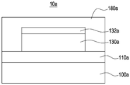
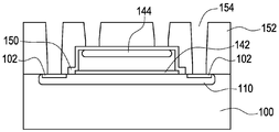
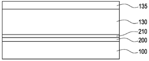
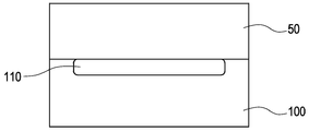
도 1은, 실리콘(Si) 기판(100a), Si 기판(100a)의 상부 표면 가까이에 위치하는 Si 기판(100a) 내 n-형 도핑된 영역(110a), Si 기판(100a)의 상부 표면 상에 배열된 진성 게르마늄(Ge) 영역(130a), 진성 Ge 영역(130a)의 상부 표면 상에 배열된 p-형 Ge 영역(132a), 및 진성 Ge 영역(130a) 및 p-형 Ge 영역(132a)을 둘러싸는 것은 물론 또한 Si 기판(100a)의 상부 표면을 덮는 산화물 패시베이션(180a)을 포함하는, 광 다이오드(10a)를 도시한다.Figure 1 shows a
도 1에 도시된 바와 같은 구조에 대해서는, Ge 영역(130a)과 기저 Si 기판(100a) 사이에 이질적 계면이 존재한다. 이질적 계면은, 성장되는 결정성 기판과는 다른 원소 구성의 결정성 재료를 성장시킴으로써 수행되는 에피택시의 유형인 헤테로에피택시를 사용함으로써 구현될 수 있다. 예는, 국한되는 것은 아니지만, 사파이어 상의 GaN, Si 상의 GaN, Si 상의 Ge을 포함한다. 결정성 재료는 원소 또는 화합물 반도체일 수 있다.1, there is a heterogeneous interface between the
일부 응용에 대해서는, 더 양호한 디바이스 성능을 위해 성장된 막 상에든 기판 상에든 전기적 진성 재료 속성이 필요하다. 진성 반도체는 전기적 중성 속성을 나타내 보이는 반도체이다. 여기에서는 10x17 cm-3 아래의 캐리어 농도를 갖는 영역이 진성이라고 생각된다. 그렇지만, 진성 재료는 때로는 이질적 계면을 획득하기가 어렵다. 격자-불일치된 결함 형성, 2개의 재료 간 상호-확산(또는 교차 확산)(하나의 재료의 성분은 때로는 다른 재료의 활성 도판트가 될 수 있음), 막 성장 동안 오염, 또는 에너지대 정렬 유발된 페르미 준위 핀잉(Fermi level pinning)에 기인하여 의도치 않게 전기적으로 분극된 층이 계면 가까이에 흔히 형성된다. 예컨대, Si 상의 Ge 시스템의 계면에는 일반적으로 p-형 Ge 층이 형성된다.For some applications, electrical intrinsic material properties are required on the grown film or on the substrate for better device performance. Inherent semiconductors are semiconductors that exhibit electrical neutrality. In this case, a region having a carrier concentration below 10 x 17 cm -3 is considered to be intrinsic. However, intrinsic materials are sometimes difficult to obtain a heterogeneous interface. Lattice-mismatched defect formation, inter-diffusion (or cross diffusion) between two materials (a component of one material can sometimes be an active dopant of another material), contamination during film growth, Due to Fermi level pinning, an unintentionally electrically polarized layer is often formed near the interface. For example, a p-type Ge layer is generally formed at the interface of the Ge system of Si.
더욱, 격자 불일치에 기인하여 이질적 계면에 형성된 그러한 전위 및 다른 유형의 결함이 반도체 공핍(depletion) 영역 내에 위치하면, 그것은 트랩-조력 캐리어 발생에 기인하여 광 다이오드의 암전류, 즉, 암조건 하에서의 누설 전류를 증가시키고 그래서 성능을 저하시킴은 물론 또한 설계 윈도우(window)를 좁힐 수 있다. 트랩-조력 발생 메커니즘은 결함 트랩 상태가 외인성 도판트 조력 캐리어로 채워져 캐리어 발생 레이트를 중화하게 되도록 고도의 도핑 농도로 이러한 결함 있는 영역을 패시베이팅함으로써 효과적으로 감축될 수 있음이 관찰된다. 이러한 도핑 패시베이션 기술을 달성하기 위해, 고도로-결함 있는 구역에서의 정밀한 도판트 제어는 때로는 결함 조력 도판트 확산의 본성에 기인하여 어렵다. 제어되지 않은 도판트 확산은, 디바이스 반응도 저하 및 수율 감소와 같은, 원치 않는 성능 및 신뢰도 페널티를 야기할 수 있다.Furthermore, if such dislocations and other types of defects formed at the heterogeneous interface due to lattice mismatch are located within the semiconductor depletion region, then it is likely that the dark current of the photodiode due to trap-assist carrier generation, Thereby reducing the performance and also narrowing the design window. It is observed that the trap-assist generation mechanism can be effectively reduced by passivating this defective area at a high doping concentration such that the defect trap state is filled with an exogenous dopant tidal carrier to neutralize the carrier generation rate. In order to achieve this doping passivation technique, precise dopant control in highly-defective regions is sometimes difficult due to the nature of defective assisted dopant diffusion. Uncontrolled dopant diffusion can cause unwanted performance and reliability penalties, such as device degradation and reduced yield.
도 1에 도시된 바와 같은 Si 상의 Ge 광 다이오드를 제조하는 구현 중 일부에서, 블랭킷 유형 에피택셜 성장이 사용되면 광학 흡수 구역(즉, 도 1에서는 진성 Ge 영역(130a))을 획정하도록 Ge 메사(mesa) 패터닝이 필요로 된다. 블랭킷 유형 에피택셜 성장은 전체 기판 웨이퍼 표면 상에 수행되는 에피택셜 성장이다. 반응성 이온 식각(RIE) 및 유도성 결합 플라스마(ICP) 식각은 블랭킷 에피택셜 성장 후에 Ge 메사를 패터닝하기 위한 공통적 방법으로서 이 경우 소망의 메사 측벽 각도는 주의 깊게 엔지니어링된 이방성 식각 레시피로 달성된다. 그렇지만, 이방성 식각은 보통은 패터닝된 구조 상의 이온 폭격을 수반하고, 흔히 Ge 측벽 표면 손상을 초래한다. 손상된 측벽 표면은 광 다이오드 암전류를 증가시키는 댕글링 본드 및 결함을 초래한다. 그러한 디바이스 저하를 회피하기 위해, 컨포멀 손상-없는 선택적 Ge 식각 접근법(Si 위에 선택적)이 이방성 식각 유발된 손상된 표면 층을 제거하도록 제시된다. 예컨대, 선택적 식각은 5 대 1 비보다 더 큰 Ge과 Si 간 식각 레이트 차이로서 정의될 수 있다.In some of the implementations for fabricating Si-phase Ge photodiodes as shown in FIG. 1, if blanket-type epitaxial growth is used, a Ge mesa (e.g., an
더 높은 동작 속도 광 다이오드 또는 광 검출기를 위해, 감광 층, 즉, 도 1에 도시된 진성 Ge 영역(130a)의 두께는 더 낮은 광-반응도의 희생으로 캐리어 주행 시간을 최소화하기에 충분히 얇을 필요가 있다. 반응도를 개선하고 여전히 고속을 유지하기 위해, 광학 반사체가 감광 층의 정상에 놓일 수 있다. 반사체 재료는 하나의 유전체 층(예컨대, 산화물 또는 질화물), 다수의 유전체 층, 금속(예컨대, 알루미늄), 또는 위에서 열거된 재료들의 어느 조합이라도 포함할 수 있다. 그러한 반사체를 형성하는 것은 목표로 하는 반사율이 소망 스펙트럼 내에 있음을 보장하도록 엄격한 두께 공차(< 5%)를 필요로 하는데, 관용적 주조 공장에는 비교적 어려울 수 있다. 본 발명에서는 소망 반사체 구조에 대한 두께 균일도 제어를 개선하도록 식각 또는 폴리싱 정지 층이 제시된다. 이하, 광 흡수 장치는 PIN 광 다이오드로서 예를 들 것이다. 그렇지만, 이러한 특정 예는 본 발명의 범위에 대한 제한은 아니다. 예컨대, NIP 구조가 또한 본 발명의 특정 구현에 의해 구현될 수 있다. 더욱, 다양한 Ge 함량을 갖는 SiGe과 같은 다른 광 흡수 재료가 사용될 수 있다.For higher operating speed photodiodes or photodetectors, the thickness of the photosensitive layer, i. E. The
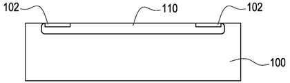
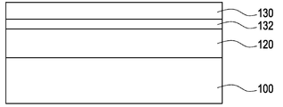
도 2a 내지 도 2f는, 이질적 계면에서 누설 전류를 감축하고 또는/그리고 동작 바이어스를 감축하도록 반대 도핑 층이 제시되는, 본 발명의 제1 실시형태에 따른 광 흡수 장치의 제조 단계를 예시하는 단면도이다. 도 2a(단계(S100))에서 도시된 바와 같이, 반도체 기판(100)이 제공되고, 기판(100)의 상부면 가까이에 n+ 도핑된 층(102)이 형성된다. n+ 도핑된 층(110)은, 국한되는 것은 아니지만, 도판트 확산 및 활성화를 위해 선택사항인 열 처리 절차와 조합된 동시 인-시츄 도핑을 갖는 에피택셜 층 성장, 기상 확산, 및 이온 주입과 같은 방법으로 형성될 수 있다. 감축된 저항 콘택트용 2개의 고도의 도핑 영역(102)은 n+ 도핑된 층(110)의 그것보다 더 고도의 도핑 레벨로 형성된다. 예컨대, 도핑 농도는 n+ 도핑된 층(110)에 대해서는 1x1019cm-3보다 더 크고, 콘택트(102)에 대해서는 1x1020cm-3보다 더 크다.2A to 2F are cross-sectional views illustrating steps of fabricating a light absorbing device according to a first embodiment of the present invention, wherein an opposite doping layer is presented to reduce leakage current and / or reduce operating bias at a heterogeneous interface . As shown in FIG. 2A (step S100), a
본 발명의 일부 실시형태에서 그리고 도 2a에서 도시된 바와 같이, 반도체 기판(100)은 벌크 반도체 기판이다. 벌크 반도체 기판이 채용될 때, 벌크 반도체 기판은, 국한되는 것은 아니지만, Si, Ge, SiGe, SiC, SiGeC, InAs, GaAs, InP 또는 다른 유사한 III/V 화합물 반도체를 포함하는 어느 반도체 재료로라도 이루어질 수 있다. 이들 반도체 재료의 다층이 또한 벌크 반도체 기판의 일부분으로서 사용될 수 있다. 일 실시형태에서, 반도체 기판(100)은, 예컨대, 단일 결정성 실리콘과 같은 단일 결정성 반도체 재료를 포함한다. 다른 실시형태에서는, SOI(semiconductor-on-insulator) 기판(구체적으로 도시되지는 않음)이 반도체 기판(100)으로서 채용된다. 채용될 때, SOI 기판은 핸들 기판, 핸들 기판의 상부 표면 상에 위치하는 매립된 절연 층, 및 매립된 절연 층의 상부 표면 상에 위치하는 반도체 층을 포함한다. SOI 기판의 핸들 기판 및 반도체 층은 동일한, 또는 다른, 반도체 재료를 포함할 수 있다. 용어 "반도체"는 핸들 기판 및 반도체 층의 반도체 재료와 연관하여 여기에서 사용될 때, 예컨대, Si, Ge, SiGe, SiC, SiGeC, InAs, GaAs, InP 또는 다른 유사한 III/V 화합물 반도체를 포함하는 어느 반도체 재료라도 나타낸다. 이들 반도체 재료의 다층이 또한 핸들 기판 및 반도체 층의 반도체 재료로서 사용될 수 있다. 일 실시형태에서, 핸들 기판 및 반도체 층 양자는 실리콘으로 이루어질 수 있다. 다른 실시형태에서는, 다른 결정학적 정향의 다른 표면 영역을 갖는 하이브리드 SOI 기판이 채용된다. 이러한 예에서, 반도체 기판(100)은 실리콘 기판(100)으로서 예를 든다.In some embodiments of the present invention and as shown in Figure 2A, the
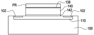
도 2b(단계(S102))에서 도시된 바와 같이, (Ge 에피택셜 층과 같은) 에피택셜-퇴적된 광 흡수 에피택셜 층(130)은 도핑된 층(110)의 정상에 형성되고, 도핑된 층(110)과 Ge 에피택셜 층(130) 사이에 반대 도핑 층(132)을 더 포함한다. 일부 구현에서, 반대 도핑 층(132)의 두께는, 계면 가까이의 도핑 프로파일에 종속하여, 1 nm 내지 150 nm 범위이다. 반대 도핑 층(132) 내부의 도판트는 전기적 중화를 위해 반대 전하 극성을 제공함으로써 계면에서 빌트인 전위/캐리어를 보상하도록 그리고 빌트인 전위 및 그리하여 동작 바이어스 및/또는 누설 전류를 감축하도록 유사한 자유 캐리어 농도를 제공할 수 있어야 한다. Si 상의 Ge 시스템에 대해, 계면은 자연적으로 p-형이고, 그래서 반대 도핑 층(132) 내부의 도판트는 바람직하게는 n-형 도판트, 예컨대, As, P 또는 그들 조합이다. 반대 도핑 층(132)은 Ge 에피택셜 층을 에피택셜 성장시키는 동안 인-시츄 도핑에 의해 형성될 수 있다. 인-시츄 도핑 공정에서, 도판트는 결정성 반도체 재료의 퇴적 동안 도입된다. 대안으로, 반대 도핑 층(132)은, 국한되는 것은 아니지만, n-형 도판트로 이온 주입과 같은 다른 접근법으로 형성될 수 있다. 반대 도핑 층은 다양한 Ge 함량을 갖는 SiGe과 같은 다른 재료 또는 층(130)과 동일한 재료일 수 있다. 일부 구현에서는, 층(130)으로 향한 확산으로부터 층(132) 도핑을 감축하도록 층(132)과 층(130) 사이에 부가적 층이 부가될 수 있다. 예컨대, 이러한 선택사항인 층은 다양한 Ge 함량을 갖는 SiGe 재료일 수 있다. Ge 에피택셜 층(130) 및 반대 도핑 층(132)이 형성된 후에, 산화물 캡(138)은 Ge 표면을 보호하도록 Ge 에피택셜 층(130) 정상에 형성된다.As shown in FIG. 2B (step S102), an epitaxially-deposited light absorption epitaxial layer 130 (such as a Ge epitaxial layer) is formed on top of the doped
도 2c(단계(S104))에서 도시된 바와 같이, 산화물 캡(138)이 형성된 후에, 리소그래피 및 식각 공정이 Ge 메사 영역(140) 및 반대 도핑 메사 영역(142)을 획정하도록 수행되어, 실리콘 기판(100)의 상부 표면 부분을 노출시킨다.After the
도 2d(단계(S106))에서 도시된 바와 같이, Ge 에피택셜 메사 영역(140) 또는/및 반대 도핑 메사 영역(142)을 측방에서 오목하게 하도록 적합한 부식제가 사용된다.As shown in FIG. 2d (step S106), a suitable etchant is used to concave the Ge
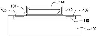
도 2e(단계(S108))에서 도시된 바와 같이, 패시베이션 층(150)은 Ge 표면을 패시베이팅하도록 결과적 구조 정상에 형성되고, p-형 도핑된 영역(144)은 이온 주입과 같은 반도체 제조 공정에 의해 Ge 메사 영역(140)의 상부 표면 가까이에 형성된다. 일부 구현에서, 패시베이션 층(150)은 비정질 실리콘(a-Si) 또는 다-결정성 실리콘(poly-Si)일 수 있다. 다른 구현에서, 영역(144)의 도핑 공정 동안, 패시베이션 층(150)은 동시에 도핑되고 살리사이드를 포함하는 콘택트 형성에 사용될 수 있다. 일부 구현에서, 도핑된 영역(144)의 구역은 상부로부터 볼 때 메사 영역(140)과는 다른 형상을 가질 수 있다. 예컨대, 메사 영역(140)의 형상은 직사각형일 수 있고, 도핑된 영역(144)의 형상은 원형일 수 있다. 일부 구현에서, 도핑된 영역(144)의 구역은 상부로부터 볼 때 메사 영역(140)과 유사한 형상을 가질 수 있다. 예컨대, 메사 영역(140)과 도핑된 영역(144)의 형상은 둘 다 직사각형 또는 원형일 수 있다.The
도 2f(단계(S110))에서 도시된 바와 같이, 층간 유전체(ILD) 층(152)은 Ge 메사에 기인하는 토포그래피로 결과적 구조의 정상에 형성되고, CMP(화학적 기계적 폴리싱) 공정은 표면 토포그래피를 감축하도록 수행된다. 층간 유전체(ILD)는 소망의 두께를 얻도록 수회 퇴적될 수 있다. 이후에, 콘택트 개구부(154)가 리소그래피 및 식각 공정을 통해 획정되어 고도로 도핑된 실리콘 표면(102) 및 패시베이션 층(150)의 일부분을 노출시킨다.As shown in Figure 2f (step S110), the interlayer dielectric (ILD)
도 2g(단계(S112))에서 도시된 바와 같이, 살리사이드(158)는 Ni, Co, Ti, Pt와 같은 금속을 도입하고 그 다음에 열 형성 가공이 따르고 그 후 미-반응 부분을 제거함으로써 실리콘 기판(102) 표면 정상에 형성된다. 그 후, 텅스텐 플러그(W 플러그)(156)는 실리사이드(158) 정상에 콘택트 개구부(154) 내에 형성된다.As shown in FIG. 2g (step S112),
도 2h(단계(S114))에서 도시된 바와 같이, 금속 상호접속부(M1 층)(160)는 외부 회로로의 전기적 접속을 제공하도록 형성된다. 일부 구현에서, 광학 신호가 도 2h의 상부로부터 입사하면, ARC 코팅은 Ge 메사 영역(140)의 상부 상에서 ILD(152)로부터 개구부를 우선 식각함으로써 광 다이오드의 상부 상에 부가될 수 있다. 일부 구현에서, 광학 신호가 도 2h의 저부로부터 입사하면, ARC 코팅은 기판을 우선 씬잉함으로써 광 다이오드의 저부 상부 상에 부가될 수 있다.As shown in Figure 2h (step S114), the metal interconnect (M1 layer) 160 is formed to provide electrical connection to external circuitry. 2h, an ARC coating may be added on top of the photodiode by first etching the opening from the
이러한 구현에서, n-형 도판트 및 적합한 두께(1 nm 내지 150 nm)를 갖는 Ge 메사 영역(140) 아래 반대 도핑 메사 영역(142)은 p-형 이질적 계면을 보상하여 빌트인 전위 및 그리하여 동작 바이어스 및/또는 누설 전류를 감축하도록 형성된다. 도 2a 내지 도 2h에서, 상부 흡수 영역 콘택트 및 기판 콘택트 양자에 대해 도시된 2개의 콘택트 지점은 2D 단면도에서 예시적 목적을 위한 것임을 주목한다. 일부 구현에서는, 기판 및 흡수 영역에 대한 단일의 연속적 콘택트 비아 또는 링이 또한 광 흡수 영역으로부터 광-발생된 캐리어를 추출하도록 형성될 수 있다. 또한, 도 2e 내지 도 2h에서, 광 흡수 영역을 덮는 것을 도시된 패시베이션 층(150)은 예시적 목적을 위한 것이고, 이러한 패시베이션 층(150)은 또한 그것이 텅스텐 플러그(W 플러그)(156) 또는 다른 형태의 콘택트 비아가 도핑된 영역(102, 144)에 전기적으로 접속하는 것을 금지하지 않는 한 다른 영역으로 확장할 수 있음을 주목한다. 더욱, 도 2e 내지 도 2h에서 세그먼팅된 도핑된 층(110)은 예시적 목적을 위한 것이고, 일부 구현에서, 그것은 다른 영역으로 확장할 수 있다. 도 2a 내지 도 2h에서 P 도핑된 층(144)은 예시적 목적을 위한 것이고, 일부 구현에서, 그것은 다른 실시형태에서 층(140)의 측벽까지 확장할 수 있다.In this implementation, the opposite doped
도 3a 내지 도 3c는 이질적 계면 가까이에 진성 영역을 형성하기 위한 다른 구현을 도시한다. 도 3a에서 도시된 바와 같이, 도 2b에 대응하는 단계(S102)는 다음의 부-단계를 갖는 단계(S102a)에 의해 더 설명될 수 있다: 반대 도핑 층(122)은 Si 기판(100)의 상부 표면 상에 형성되고, 여기서 반대 도핑 층(122)은 이온 주입에 의해 형성될 수 있다. 이후에, 층(130)이 형성된다. 도 3b에서 도시된 바와 같이, 도 2b에 대응하는 단계(S102)는 다음의 부-단계를 갖는 단계(S102b)에 의해 교체될 수 있다: 제1 반대 도핑 층(122a)은 Si 기판(100)의 상부 표면 상에 형성되고, 여기서 제1 반대 도핑 층(122a)은 이온 주입에 의해 형성될 수 있다. 이후에 에피택셜-성장된 Ge 층(130)이 기판(100)의 정상에 형성되고, Ge 에피택셜 층(130)은 제2 반대 도핑 층(132a)을 갖는다. 이질적 계면은 제1 반대 도핑 층(122a)(Si-계 재료)과 제2 반대 도핑 층(132a)(Ge-계 재료) 사이에 존재한다. 일부 구현에서, 제1 반대 도핑 층(122a)의 두께는, 계면 가까이의 도핑 프로파일에 종속하여, 1 nm 내지 150 nm 범위이다. 더욱, 제1 반대 도핑 층(122a) 내부의 도판트는 전기적 중화를 위해 반대 전하 극성으로 Ge 에피택셜 층(130)에서의 그들 빌트인 전위/캐리어와 유사한 자유 캐리어 농도를 제공할 수 있어야 한다. 일부 구현에서, 제2 반대 도핑 층(132a)의 두께는 1 nm 내지 150 nm 범위이다. 더욱, 제2 반대 도핑 층(132a) 내부의 도판트는 p-형 계면 결함 및 헤테로접합 정공 가둠에 의해 야기된 Ge과 Si 간 P-형 계면에 기인하여 전기적 중화를 위해 반대 전하 극성으로 Si/Ge 계면에서의 그들 빌트인 전위/캐리어와 유사한 자유 캐리어 농도를 제공할 수 있어야 한다.Figures 3A-3C illustrate another implementation for forming an intrinsic region near a heterogeneous interface. 3A, step S102 corresponding to FIG. 2B can be further illustrated by step S102a having the following sub-steps: the
도 3c에서 도시된 바와 같이, 도 2b에 대응하는 단계(S102)는 다음의 부-단계를 갖는 단계(S102c)에 의해 교체될 수 있다. Si 에피택셜 층(120)은 Si 기판(100) 상에 형성된다. Si 기판(100)은 에피택셜 층(120) 가까이의 계면에서 도핑될 수 있다. 에피택셜-성장된 Ge 층(130)은 Si 에피택셜 층(120)의 정상에 형성되고, Ge 층(130)은 반대 도핑 층(132)을 더 포함한다. 반대 도핑 층(132)의 두께는 1 nm 내지 150 nm 범위이고 바람직하게는 p-형 계면을 보상하도록 n-형 도판트, 예컨대, As, P 또는 그들 조합에 의해 도핑된다. 반대 도핑 층(132)은 n-형 불순물로 이온 주입에 의해 또는 Ge 층을 에피택셜 성장시키는 동안 인-시츄 도핑에 의해 형성될 수 있다. 일부 구현에서, Si 에피택셜 층(120)은 도핑된 기판으로부터의 도판트 확산을 감축하는 것, 또는/및 Ge보다 더 작은 그 유전율에 기인하는 접합 커패시턴스를 감축하는 것을 포함하는 다수의 목적을 제공할 수 있다.As shown in FIG. 3C, step S102 corresponding to FIG. 2B may be replaced by step S102c having the following sub-steps.
도 2b 내지 도 2h에서 도시된 예에서, 반대 도핑 층 또는 반대 도핑 메사는 실리콘 층과 게르마늄을 포함하는 다른 에피택셜 층 간 계면 층이라고 넓게 지칭될 수 있다. 반대 도핑 층의 주요 조성은 실리콘 또는 게르마늄 또는 그들 합금 중 어느 것일 수 있다. 도 3a에서 도시된 예에서, 반대 도핑 층(122)은 실리콘 기판(100)과 Ge 에피택셜 층(130) 간 계면 층이라고 넓게 지칭될 수 있다. 도 3b에서 도시된 예에서, 제1 반대 도핑 층(122a) 및 제2 반대 도핑 층(132a)은 이러한 예에서 2개의 층이 수반되더라도 실리콘 기판(100)과 Ge 에피택셜 층(130) 간 계면 층이라고 넓게 지칭될 수 있다. 도 3c에서 도시된 예에서, 반대 도핑 층(132)은 Si 에피택셜 층(120)이 실리콘 기판(100)과 반대 도핑 층(132) 사이에 샌드위치되더라도 실리콘 기판(100)과 Ge 에피택셜 층(130) 간 계면 층이라고 넓게 지칭될 수 있다. 본 발명에서, 계면 반대 도핑 층은 층(A)과 층(B) 간 단일 층 또는 다수 층일 수 있고, 층(A)과 층(B) 간 진성 영역을 제공한다. 더욱, 계면 층은 층(A) 및 층(B) 중 하나와 직접 접촉하고 있을 필요는 없고, 층(A)과 층(B) 사이에 실질적 진성 영역이 존재할 수 있는 한 계면 층과 층(A) 사이에 또는 계면 층과 층(B) 사이에 다른 층이 개재될 수 있다.In the example shown in Figures 2b-2h, the opposite doped layer or opposite doped mesa can be broadly referred to as an interfacial layer between the silicon layer and another epitaxial layer comprising germanium. The major composition of the opposite doping layer may be silicon or germanium or alloys thereof. In the example shown in FIG. 3A, the opposite doped
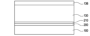
도 4a 내지 도 4c는 본 발명의 일 구현에 따라 결함 조력 도판트 확산이 감축된 광 다이오드를 형성하는 제조 단계를 예시하는 단면도이다. 도 4a에서 도시된 바와 같이, 도핑 층(200)은 에피택셜 성장에 의해서든 이온 주입에 의해서든 기판 재료(100)의 정상에 형성된다. 그 후, 도판트 제어 층(210)이 도핑 층(200) 위에 형성된다. 일부 구현에서, 도판트 제어 층(210)은 실리콘 게르마늄을 포함하고, 도핑 층(200)은 게르마늄 또는 실리콘 게르마늄을 포함하고, 도핑 층(200) 내부의 도판트는 인(P)을 포함한다. Ge을 포함하는 에피택셜 층(130)은 감광 영역으로서 도판트 제어 층(210)의 정상에 형성되고, 상부 도핑된 층(135)은 에피택셜 층(130)의 정상에 형성된다. 일부 구현에서, 상부 도핑된 층(135)에서의 도판트는 붕소(B)를 포함한다.Figures 4A-4C are cross-sectional views illustrating a fabrication step for forming a photodiode with reduced defibrillator dopant diffusion in accordance with an embodiment of the present invention. As shown in FIG. 4A, the
일부 구현에서, 도핑 층(200)은 기판 재료(100)로부터의 도판트를 최초에 도핑되지 않은 (200) 층 영역으로 추진함으로써 형성될 수 있다. 추진 공정은 도판트 제어 층(210) 및 에피택셜 층(130)의 적어도 일부분이 형성된 후에 행해질 수 있다. 에피택셜 층(130)의 재료는, 국한되는 것은 아니지만, Si, 1% 내지 100%의 Ge 함량을 갖는 SiGe일 수 있다. 도판트 제어 층(210)의 재료는, 국한되는 것은 아니지만, 에피택셜 층(130)으로부터의 그것보다 더 적은 Ge 함량을 갖는 SiGe, 탄소-도핑된 SiGe, 또는 탄소-도핑된 Ge일 수 있다. 도핑 층(200)의 재료는, 국한되는 것은 아니지만, 고도로-도핑된 Ge, 에피택셜 층(130)보다 더 높지 않고 도판트 제어 층(200)보다 더 적지 않은 Ge 함량을 갖는 고도로-도핑된 SiGe일 수 있다.In some implementations, the
도핑된 층(200)은 Si 기판(100)의 그것과 동일한 전기적 극성을 갖는다(예컨대, n-형 도핑). Si 기판(100)이 격자 불일치로 Ge 에피택셜 층(130)과 직접 접촉하고 있으면, 그것은 결함을 유발하고 더 높은 암전류 및 더 빠른 도판트 확산을 초래할 것이다. 결과로서, 도판트 제어 층(210)은 에피택셜(130) 영역으로 더 깊이 가서 디바이스 저하를 초래함이 없이 결함 상태를 패시베이팅함으로써 암전류 발생을 감축하기 위해서 기판(100)으로부터의 도판트가 도핑 층(200)으로만 추진될 수 있게 하도록 도판트 블록으로서 Si/Ge 계면 가까이에 놓도록 설계된다. 일부 구현에서, 도핑된 층(200)은 동작 바이어스 및/또는 누설 전류를 감축하도록 앞서 설명된 바와 같은 반대 도핑 층으로서 기능할 수 있다.The doped
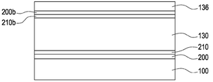
도 4b에서 도시된 바와 같이, 그것은 상부 도핑된 층(135)이 아래 감광 재료와는 다른 재료 조성을 갖는 이질적 상부 도핑된 층(136)으로 교체되어 있다는 것을 제외하고는 도 4a와 유사하다. 이질적 도핑된 층(136)은 Ge 에피택셜 층(130)과 이질적 상부 도핑된 층(136) 간 경미한 또는 영 격자 불일치가 도입되도록 Si 또는 SiGe로 제작된다.As shown in FIG. 4B, it is similar to FIG. 4A except that the top
도 4c에서 도시된 바와 같이, 그것은 이질적 계면 품질을 개선하도록 감광 재료와 상부 도핑된 층(136) 사이에 다른 세트의 도핑 층(200b)과 도판트 제어 층(210b)이 도입되어 있다는 것을 제외하고는 도 4b와 유사하다. 도판트 제어 층(210b)은 상부 도핑된 층(136)으로부터 감광 영역(130)으로 도판트 확산을 감축하도록 도입된다. 상부 도핑된 층(136)은 Si, Ge, 또는 그들 조합을 포함할 수 있다. 상부 도핑된 층(136)에서의 도판트는 B, P, As, 및 그들 조합을 포함할 수 있다. 일부 구현에서, 도핑 층(200b)은 상부 도핑된 층(136)과 동일한 도핑 극성을 가질 수 있다. 일부 구현에서, 도핑 층(200b)은 계면 빌트인 전위를 감축하고, 동작 바이어스를 감축하도록 앞서 설명된 바와 같은 반대 도핑 층으로서 기능할 수 있다.As shown in FIG. 4C, except that another set of doped
도 4a 내지 도 4b에서 도시된 예에서, 도핑된 층(200) 및 도판트 제어 층(210)은 그들 예에서 Si 기판(100)과 에피택셜 층(130) 사이에 2개의 층이 있더라도 Si 기판(100)과 에피택셜 층(130) 간 계면 층이라고 지칭될 수 있다. 유사하게, 도 4c에서 도시된 예에서, 도핑 층(200b) 및 상부 도판트 제어 층(210b)은 상부 도핑된 층(136)과 에피택셜 층(130) 간 계면 층이라고 지칭될 수 있다. 본 발명에서, 계면 층은 층(A)과 층(B) 간 단일 층 또는 다수 층이고, 층(A)과 층(B) 간 도판트 확산을 제어할 수 있다. 더욱, 계면 층은 층(A) 및 층(B) 중 하나와 직접 접촉하고 있을 필요는 없고, 도판트 확산이 층(A)과 층(B) 간 계면 층 내에서 제어될 수 있는 한 계면 층과 층(A) 사이에 또는 계면 층과 층(B) 사이에 다른 층이 개재될 수 있다. 일부 구현에서, 도판트 제어 층과 도핑 층의 상대적 위치는 교환될 수 있다, 즉, 도판트 제어 층은 도핑 층 위에든 아래에든 있을 수 있다. 일부 구현에서, 도핑 층은 앞서 설명된 바와 같은 반대 도핑 층으로서 기능할 수 있다.4A-4B, the doped
도 5a 내지 도 5b는 도 4a에서 도시된 구조의 일 구현을 도시한다. 진성-Ge를 포함하는 에피택셜 층(130)은 에피택셜 층(130)과 유사한 재료 조성을 갖는 시드 층(200)을 우선 성장시키고, 그 후 빠르게 확산하고 소망 진성 속성을 발휘하지 못하게 할 수 있는 에피택셜 Ge 층으로의 인 확산을 감축하도록 Si 또는 SiGe 기능을 포함하는 도판트 제어 층(210)을 성장시킴으로써 N-형 인-도핑된 Si 기판(100) 상에 성장된다. 시드 층(200) 및 도판트 제어 층(210)의 두께 및 위치는 성장 동안 잘 제어될 수 있다. 일부 구현에서, 도판트 제어 층(210)은 50 nm 내지 150 nm 범위이고 SiGe를 포함한다. 도 5b에서 도시된 바와 같이, Si 기판(100)의 상부 층과는 반대의 전기적 극성을 갖는, 상부 도핑된 층(135)은 p-i-n 광 다이오드/광 검출기 구조를 내놓도록 형성된다.Figures 5A-5B illustrate one implementation of the structure shown in Figure 4A. The
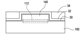
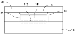
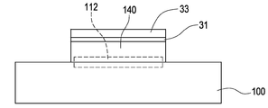
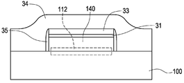
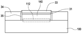
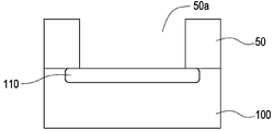
도 6a 내지 도 6e는 본 발명의 다른 구현에 따라 식각/폴리싱 스토퍼를 갖는 광 다이오드를 형성하는 제조 단계를 예시하는 단면도이다. 도 6a에서 도시된 바와 같이, 공정은 도 2d에서 도시된 단계(S106)를 계승할 수 있다. 도핑된 영역(102, 110)은 단순 예시 목적을 위해 여기에서는 생략된다. 제1 계면 층(112)은 Si 기판(100)의 정상에 형성되고, Ge를 포함하는 제2 층(140)은 제1 계면 층(112)의 정상에 형성된다. (파선 박스로서 도시된) 제1 계면 층(112)은 도 2a 내지 도 3c를 참조하여 설명된 바와 같은 반대 도핑에 사용되거나, 또는 도 4a 내지 도 4c를 참조하여 설명된 바와 같은 확산 제어에 사용되거나, 또는 대역폭 조절을 위해 제2 층(140)의 그것보다 더 큰 유전율을 갖는 재료일 수 있다. 또한, 도 6a에서 도시된 바와 같이, 국한되는 것은 아니지만, Si(비정질 또는 다-결정성), 실리콘 산화물, 질화물, 하이-k 유전체, 또는 그들 조합과 같은 재료를 갖는 패시베이션 층(30)이 제2 층(140)을 패시베이팅하여 보호하도록 형성된다.Figures 6A-6E are cross-sectional views illustrating fabrication steps for forming photodiodes having etch / polishing stoppers in accordance with another embodiment of the present invention. As shown in Fig. 6A, the process can inherit the step S106 shown in Fig. 2D. The doped
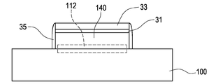
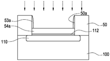
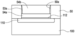
도 6b에서 도시된 바와 같이, 국한되는 것은 아니지만, 질화물과 같은 재료를 갖는 정지 층(32)이 패시베이션 층(30)의 정상에 블랭킷 층으로서 형성된다. 일부 구현에서, 정지 층은 또한 산화물 및 질화물을 포함하는 다수의 층을 포함할 수 있다. 일부 구현에서, 정지 층(32)의 두께는 전형적으로, 국한되는 것은 아니지만, 10A 내지 2000A의 범위이며, 100A 내지 500A의 두께가 더 전형적이다. 이후에, 층간 유전체(ILD) 층(34)은 그 후 전체 메사 구조를 덮도록 퇴적되고, 선택사항으로서는 도 6c에서 도시된 바와 같이 리플로우 또는 화학적 기계적 폴리싱(CMP) 공정 중 어느 것에 의해 우선 예비-평탄화될 수 있다. ILD 층(34)은, 국한되는 것은 아니지만, 정지 층(32)과는 다른 재료 조성을 갖는 실리콘 산화물과 같은 재료를 사용한다. 도 6d에서 도시된 바와 같이, ILD 층(34)은 정지 층(32)의 정상의 ILD 층(34)의 부분이 실질적으로 제거될 때까지 CMP 공정에 의해 가공된다. 도 6c에서의 예비-평탄화 공정이 수행되지 않으면, 그때는 CMP와 같은 단일 평탄화 공정이 도 6d에서의 구조를 형성하도록 사용될 수 있다. 더 구체적으로, 제거 공정은 최소 두께 손실로 메사 정지 층(32)의 상부 상에서 완전히 종단하도록 설계된다. 즉, ILD 층(34)에 대한 제거 공정은 정지 층(32)에 대해 고도로 선택적일 필요가 있다. 예컨대, 선택도는 1:5보다 더 클 수 있다. 이후에, 도 6e에서 도시된 바와 같이, 반사체(36)가 그 후 정지 층(32)의 상부 상에 균일하게 퇴적된다. 이러한 접근법으로, 상부 반사체(36)의 두께 균일도는 폴리싱 공정 대신에 막 퇴적 단계에 의해 잘 제어될 수 있으며, 관용적 평탄화 공정보다 더 양호한 균일도 제어를 의미한다. 반사체(36)는 광학 캐비티 경로 길이 튜닝 또는 반사 또는 양 조합 중 어느 것에 사용된다. 일부 구현에서, 유전체 층의 상부 상의 금속 층을 포함하는 반사체는 >95% 반사율을 달성할 수 있되, 도 6e의 저부로부터 입사하는 광학 신호는 제2 층(140)의 추가적 흡수를 위해 반사될 수 있다. 일부 구현에서, 산화물 또는 질화물을 포함하는 반사체는 50%보다 더 작은 반사율을 달성하도록 형성될 수 있고, 광학 신호는 도 6e의 상부로부터 입사할 수 있다. 일부 구현에서는, 반사-방지-코팅(ARC) 층이 외부 광학 소스와 제2 층(140) 사이에 부가될 수 있다. 반사체는 하나의 유전체 층(예컨대, 산화물 또는 질화물), 다수의 유전체 층, 금속(예컨대, 알루미늄), 또는 위에서 열거된 재료들의 어느 조합이라도 포함할 수 있다. 일부 구현에서, 반사체(36)는 산화물과 같은 유전체, 또는 알루미늄과 같은 금속 층, 또는 유전체 층의 상부 상의 금속 층을 포함할 수 있으며 그 두께는 입사 광의 사분의 일-실효-파장에 가까울 수 있다. 반사체는 일반적으로 높은 광학 수율을 보장하도록 고유한 그리고 엄격한 두께 공차(< 5%)를 가지고, 이러한 구현에서, 정지(식각 또는 폴리싱 정지) 층(32)은 광 다이오드/광 검출기 구조에 제공되어 반사체 구조의 두께 균일도 제어를 개선할 것이다. 위에서 제공된 공정 흐름은 특별한 순서로 서술된 것은 아니고 어느 순서로라도 재배열될 수 있음을 주목한다. 예컨대, 정지 층(32) 상의 CMP 공정 유발된 두께 변동이 더 감축될 수 있도록 정지 층(32)을 더 제거하기 위한 다른 식각 공정이 반사체를 퇴적시키기 전에 부가될 수 있다. 일부 구현에서, 정지 층(32)은 질화물이고, 인산을 포함하는 습식 식각 공정이 반사체(36)를 퇴적시키기 전에 질화물을 제거하도록 사용된다. 더욱, 위의 예에서, Ge 에피택셜 메사 영역을 형성하는 제2 층(140)은 Si 기판(100)의 표면과의 격자 불일치를 갖고, 반사체(36)는 광학 신호가 지나가 반사체(36)에 의해 반사될 때 소정 반사율이 달성될 수 있도록 소정 두께를 갖고, 광학 신호의 적어도 일부분은 제2 층(140)에 의해 흡수된다.As shown in FIG. 6B, but not limited to, a
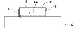
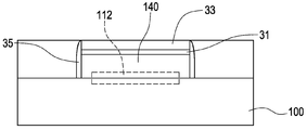
도 7a 내지 도 7e는 본 발명의 또 다른 구현에 따라 식각/폴리싱 스토퍼를 갖는 광 다이오드/광 검출기를 형성하는 제조 단계를 예시하는 단면도이다. 도 7a에서 도시된 바와 같이, 공정은 도 2b에서 도시된 단계(S102)를 계승할 수 있다. 계면 층(112)은 도 2a 내지 도 3c를 참조하여 설명된 바와 같은 반대 도핑에 사용되거나, 또는 도 4a 내지 도 4c를 참조하여 설명된 바와 같은 확산 제어에 사용되거나, 또는 대역폭 조절을 위해 제2 층(140)의 그것보다 더 큰 유전율로 형성될 수 있다. 국한되는 것은 아니지만, Si(비정질 또는 다-결정성) 또는 실리콘 산화물 또는 질화물 또는 그들 조합과 같은 재료를 갖는 패시베이션 층(31)이 결과적 구조 상에 형성된다. 이후에, 국한되는 것은 아니지만, 질화물과 같은 재료를 갖는 정지 층(33)이 패시베이션 층의 정상에 형성된다. 정지 층(33)의 두께는 전형적으로는 10A 내지 2000A이며, 100A 내지 500A의 두께가 더 전형적이다. 패시베이션 층(31), 정지 층(33) 및 기저 Ge 에피택셜 층(140)은 그 후 도 7a에서 도시된 메사 구조를 형성하도록 동시에 패터닝된다. 그 후, 도 7b에서, 패시베이션 스페이서(35)는 (패시베이션 층(31), 정지 층(33) 및 Ge 에피택셜 메사 영역(140)을 포함하는) 메사 측벽 상에 형성된다. 일부 구현에서, 패시베이션 스페이서는 측벽 가까이에 비교적 더 두꺼운 영역을 초래하도록 메사 상에 패시베이션 막을 우선 컨포멀 퇴적시킴으로써 형성된다. 그 후, 방향성(이방성) 식각이 필드 상의 스페이서 재료를 제거하도록 적용되어, 비교적 더 두꺼운 층을 갖는 측벽 영역만을 여전히 스페이서로서 있게 남긴다. 이후에, 층간 유전체(ILD) 층(34)은 그 후 전체 메사 구조를 완전히 덮도록 퇴적되고, 선택사항으로서는 도 7c에서 도시된 바와 같이 리플로우 또는 화학적 기계적 폴리싱(CMP) 공정 중 어느 것에 의해 예비-평탄화될 수 있다. 도 7d에서 도시된 바와 같이, ILD 층(34)은, 예비-평탄화 공정이 도 7c에서 처리되든 아니든, 정지 층 영역(33)의 정상의 ILD 층(34)의 부분이 실질적으로 제거될 때까지 CMP 공정에 의해 가공된다. 도 7c에서의 예비-평탄화 공정이 수행되지 않으면, 그때는 단일 폴리싱 공정이 도 7d에서의 구조를 형성하도록 사용될 수 있다. 이후에, 도 7e에서 도시된 바와 같이, 반사체(36)는 그 후, 도 6e에서 설명된 것과 유사하게, 정지 층 영역(33)의 상부 상에 균일하게 퇴적된다.7A-7E are cross-sectional views illustrating fabrication steps for forming a photodiode / photodetector with an etch / polishing stopper in accordance with another embodiment of the present invention. As shown in Fig. 7A, the process may inherit the step S102 shown in Fig. 2B. The
도 8a 내지 도 8f는 본 발명의 또 다른 구현에 따라 식각/폴리싱 스토퍼를 갖는 광 다이오드/광 검출기를 형성하는 제조 단계를 예시하는 단면도이다. 도 8a 내지 도 8c에 의해 예시된 초기 단계는 도 7a 내지 도 7c의 설명과 유사하고, 도 8d에서, ILD 층(34)은 CMP 공정 또는 에치 백 공정에 의해 더 가공되고, 공정은 ILD(34) 또는 정지 층(33) 중 어느 것 상의 다소의 초과-폴리싱 또는 초과-식각으로 정지 층 영역(33) 가까이에서 정지한다. 도 7에 비해, 이러한 구현에서, 정지 층(33)은 그것이 추후 공정에서 제거되기 때문에 더미 정지 층이라고 지칭될 수 있고, 그래서, 제거 공정은 앞서 설명된 바와 같이 정지 층에 선택적일 필요가 없고, 그리하여 공정 융통성을 더 개선한다. 도 8e에서 도시된 바와 같이, 더미 정지 층(33)은 그 후 습식 화학적 공정 또는 습식과 건식 식각 공정의 조합에 의해 제거된다. 선택된 화학물질은 정지 층(33)과만 반응하고 ILD(34)와 같은 노출된 재료의 나머지에 고도로 선택적일 수 있다. 예컨대, 정지 층이 질화물이면, 인산계 습식 식각 공정이 사용될 수 있다. 이후에, 도 8f에서 도시된 바와 같이, 반사체(36)는 그 후 도 6e 및 도 7e에서 설명된 바와 같이 결과적 구조의 상부 상에 균일하게 퇴적된다. 이러한 접근법으로, 상부 반사체(36)의 두께 균일도는 폴리싱 공정 대신에 막 퇴적 단계에 의해 잘 제어될 수 있으며, 관용적 평탄화 공정보다 더 양호한 균일도 제어를 의미한다.8A-8F are cross-sectional views illustrating fabrication steps for forming a photodiode / photodetector having an etch / polishing stopper in accordance with another embodiment of the present invention. 8A to 8C, the
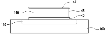
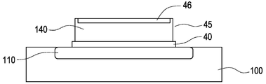
도 9a 내지 도 9d는 본 발명의 다른 구현에 따라 컨포멀 선택적 Ge 식각으로 광 다이오드/광 검출기를 형성하는 제조 단계를 예시하는 단면도이다. 도 9a에서 도시된 바와 같이, 공정은 도 2b에서 도시된 단계(S102)를 계승할 수 있으며 계면 층(40)이 에피택셜 층(130)과 기저 Si 기판(100) 사이에 놓인다. 일부 구현에서, 에피택셜 층(130)은 Ge을 포함하고, 계면 층(40)은 반대 도핑 층, 도판트 확산 층 또는 양자로서 기능하는 진성 Si 층일 수 있고, 유전체 재료로 제작된 패시베이션 층(42)은 에피택셜 층(130) 상에 형성된다. 이후에, 도 9b에서 도시된 바와 같이, 패시베이션 층(42), 기저 에피택셜 층(130) 및 계면 층(40)은 메사 구조(140)를 형성하도록 전적으로 또는 부분적으로 RIE에 의해 패터닝된다. 방향성 이온 식각(예컨대, RIE)의 수반으로, 그것은 도 9b에서 도시된 바와 같이 메사 측벽 가까이에 에피택셜 층에 대한 손상 구역(43)을 야기한다. 도 9c에서 도시된 바와 같이, 선택적 Ge 식각이 손상된 구역(43)을 제거하도록 수행된다. 이러한 공정은 도 9c에서 도시된 바와 같은 측방 오목부(45)를 야기할 것이다. 에피택셜 층(130)의 상부 표면이 유전체 패시베이션 층(42)에 의해 덮여 있므로, 식각 공정은 대부분 메사 측벽 상에서 활성이다. 이러한 컨포멀 선택적 Ge 식각을 수행하는 방법은 이하의 설명에서 더 논의될 것이다. 마지막으로, 도 9d에서 도시된 바와 같이, p-i-n 또는 n-i-p 구조를 형성하기 위해, 상부 표면 가까이의 에피택셜 층의 얇은 층(46)은 기판 도핑된 영역(110)과는 반대의 그 전기적 극성을 갖는 고도로-도핑된 층으로 변환된다. 위에서 서술된 공정은 특정 순서로 한정되지 않음을 주목한다.9A-9D are cross-sectional views illustrating fabrication steps for forming a photodiode / photodetector in a conformal selective Ge etch in accordance with another embodiment of the present invention. As shown in FIG. 9A, the process can inherit step S102 shown in FIG. 2B and an
재차 도 9c를 참조하면, 컨포멀 선택적 Ge 식각을 달성하기 위한 3개의 가능한 방법이 더 설명될 수 있다. 제1 접근법은 Si에 대한 선택도를 갖는 컨포멀(등방성) Ge 식각을 달성하도록 습식 화학적 식각을 사용하는 것이다. 전형적 Ge 식각은 보통은 2개의 단계로 수행된다. 제1 단계는 식각된 재료가 더 높은 산화 상태로 변환되는 산화 반응이다. 제2 단계는 산화 생성물의 용해를 초래한다. 일 구현에서, 습식 식각 화학 반응은 국한되는 것은 아니지만 NH4OH(용해) 및 H2O2(산화제)를 포함한다. 식각 레이트는 H2O 희석 레벨에 의해 제어될 수 있다. 더욱, 이러한 식각 화학 반응은 Si에 대한 식각 선택도를 갖는다. 혼합된 NH4OH 및 H2O2는 웨이퍼 세정을 위해 Si 산업에서 사용되고 매우 낮은 Si 식각 레이트로 알려져 있다. 제2 접근법은 하류 플라스마 구성으로 불소, 염소, 및 브롬-계 RIE 공정을 사용하는 것이다. Ge은 이온 폭격의 조력 없이 위의 화학 반응에 대해 더 반응성 있음이 관찰된다. 하류 플라스마 구성은 방향성 이온 폭격으로부터의 추가적 측벽 손상을 야기하지 않고 거의 손상 없는 컨포멀 식각을 제공할 수 있다. RIE 조건을 적절히 튜닝함으로써, 40 대 1보다 더 큰 Ge과 Si 간 식각 레이트 차이가 이러한 접근법을 사용하여 달성될 수 있다. 제3 접근법에 대해, 고온 기상 HCl 식각이 감축된 또는 낮은 압력 진공 시스템 하에서 수행된다. HCl은 Si 및 Ge을 식각할 수 있는 기체 화학 반응을 갖는다. 이것은 어느 방향성 이온 폭격으로부터의 조력도 없는 기상 식각이므로, 반응이 컨포멀이다. 더욱, Ge 및 Si를 식각하는 활성화 온도가 (100C 이상) 매우 다르고, 그리하여 600C 가까이에서 식각 공정을 동작시킬 때, Ge만이 이러한 온도 범위에서 식각될 것이고, 그리하여 Si와 Ge 간 식각 선택도를 생성한다. 더욱, 위에서 언급된 공정은 본 개시의 다른 곳에서, 예컨대, 도 6 내지 도 8에서 도시된 도면에서 언급된 다른 광 다이오드 구현에 적용될 수 있다. 예컨대, 도 7a 및 도 8a에서, 메사 형성 후에, 컨포멀 선택적 Ge 식각 공정이 도입되어 제2 층(140)의 손상된 측벽의 일부분을 제거하여, 손상되지 않은 제2 층만을 선택된 구역 내에 남기고, 그 후 제2 층(140)의 노출된 측벽의 적어도 일부분을 덮는 앞서 언급된 바와 같은 스페이서 층(35)을 형성한다.Referring again to Figure 9c, three possible ways to achieve conformal selective Ge etching can be further described. The first approach is to use wet chemical etching to achieve a conformal (isotropic) Ge etch with selectivity to Si. A typical Ge etch is usually performed in two steps. The first step is an oxidation reaction in which the etched material is converted to a higher oxidation state. The second step results in the dissolution of the oxidation product. In one embodiment, the wet etch chemistry includes, but is not limited to, NH 4 OH (dissolved) and H 2 O 2 (oxidizing agent). The etch rate can be controlled by the H 2 O dilution level. Moreover, this etch chemistry has etch selectivity to Si. Mixed NH4OH and H2O2 are used in the Si industry for wafer cleaning and are known for a very low Si etch rate. A second approach is to use fluorine, chlorine, and bromine-based RIE processes in a downstream plasma configuration. Ge is observed to be more reactive to the above chemical reactions without the aid of ion bombardment. The downstream plasma configuration can provide nearly intact conformal etching without causing additional sidewall damage from the directional ion bombardment. By properly tuning the RIE conditions, a Ge-Si etch rate difference greater than 40 to 1 can be achieved using this approach. For the third approach, hot gaseous HCl etching is performed under a reduced or low pressure vacuum system. HCl has a gas chemistry that can etch Si and Ge. This is a gas phase etch with no assist from any directional ion bombardment, so the reaction is conformal. Furthermore, when the activation temperature for etching Ge and Si is very different (above 100C), and thus when operating the etch process near 600C, only Ge will be etched in this temperature range, thus creating etch selectivity between Si and Ge . Moreover, the above-mentioned process can be applied elsewhere in this disclosure, for example, to other photodiode implementations mentioned in the drawings shown in Figs. For example, in Figures 7A and 8A, after forming the mesa, a conformal selective Ge etch process is introduced to remove a portion of the damaged side wall of the
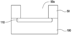
도 9e는 도핑 격리가 있는 광 다이오드를 도시하는 단면도이다. 이러한 구현에서, 2개의 흡수 요소는 흡수 요소의 2개의 인접하는 부분들 사이에 반대 도핑 영역을 생성함으로써 획정되고, 각각의 요소는 그 자신의 상부 도핑 영역 및 그 기판 도핑 영역을 갖는다. 예컨대, 기판 도핑이 양 요소에 대해 N-형이면, 그때 도핑 분리 영역은 P-형이다. 일부 구현에서, 광 흡수 영역이 약간 P-형이면, 그때 도핑 분리 영역은 N-형이다. 일부 구현에서, 흡수 영역이 Ge을 포함하고, 기판이 Si이면, 그들 계면 층은 SiGe 계면 가까이의 표면 트랩 상태에 기인하여 P-형일 수 있고, 그때 도핑 분리는 N-형이다. 여기에서의 계면 층(40)은 앞서 설명된 바와 같이 의도적으로 도판트 확산 제어 층 또는 반대 도핑 층으로서 도입될 수 있거나; 또는 그것은 Ge 에피택셜 성장 열 공정 동안 상부 Ge 층과 Si 기판 간 상호-확산 영역을 표시할 수 있다.9E is a cross-sectional view showing a photodiode with doping isolation. In this implementation, the two absorption elements are defined by creating opposite doped regions between two adjacent portions of the absorbing element, each having its own top doped region and its substrate doped region. For example, if the substrate doping is N-type for both elements, then the doped isolation region is P-type. In some implementations, if the light absorbing region is slightly P-type, then the doping separation region is N-type. In some implementations, if the absorption region comprises Ge and the substrate is Si, the interface layers may be P-type due to surface trap states near the SiGe interface, where the doping separation is N-type. The
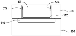
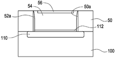
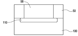
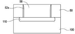
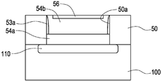
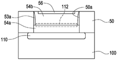
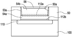
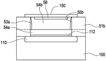
도 10a 내지 도 10f는 본 발명의 일 구현에 따라 측벽 패시베이션을 갖는 광 다이오드를 형성하는 제조 단계를 예시하는 단면도이다. 도 10a에서 도시된 바와 같이, 공정은 도 2a에서 도시된 단계(S100), 즉, 도핑된 층(110)을 갖는 Si 기판(100)을 계승할 수 있다. 그 후, (필드 유전체 층과 같은) 격리 층(50)이 Si 기판(100)의 상부 표면 상에 퇴적된다. 도 10b에서 도시된 바와 같이, 선택적 구역 개구부(50a)는 포토리소그래피 및 식각에 의해 필드 유전체 층(50)에 획정되되, 선택적 구역 개구부(50a)는 도핑된 층(110)의 표면의 일부분(제1 선택된 구역)을 노출시켰다. 이후에, 도 10c에서 도시된 바와 같이, 패시베이션 층(52)은 선택적 구역 개구부(50a)를 갖는 필드 유전체 층(50)의 상부면 상에 퇴적된다. 일부 구현에서, 패시베이션 층(52)은 Si(비정질 또는 다-결정성), 질화물, 또는 하이-k 유전체이다. 도 10d에서 도시된 바와 같이, 방향성 식각은 패시베이션 층(52)의 일부분을 제거하도록 수행되고, 패시베이션 스페이서(52a)만이 선택적 구역 개구부(50a)의 측벽(즉, 필드 유전체 층(50)의 내측 표면) 상에 남는다. 도 10e에서 도시된 바와 같이, (Ge을 포함하는 감광 재료 층과 같은) 제1 광 흡수 층은 선택적으로 성장되고, 선택적 구역 개구부(50a)를 채우고, 그 후 그것은 감광 영역(54)을 형성하도록 CMP 공정에 의해 평탄화된다. 제1 광 흡수 층을 선택적으로 성장시키기 전에, 선택사항으로서 계면 층(112)이 제1 선택된 구역의 정상에 형성될 수 있다. 계면 층(112)은 도 2a 내지 도 3c를 참조하여 설명된 바와 같은 반대 도핑 층이거나, 또는 도 4a 내지 도 4c를 참조하여 설명된 바와 같은 도판트 확산 제어 층이거나, 또는 감광 영역(54)의 그것보다 더 작은 유전율을 갖는 대역폭 조절 층일 수 있다. 마지막으로, 도 10f에서 도시된 바와 같이, 도핑된 영역(56)이 표면 가까이에 감광 영역(54) 내에 형성된다. 일부 구현에서, 도핑된 영역(56)의 구역은 상부로부터 볼 때 감광 영역(54)과는 다른 형상을 가질 수 있다. 예컨대, 감광 영역(54)의 형상은 직사각형일 수 있고, 도핑된 영역(56)의 형상은 원형일 수 있다. 일부 구현에서, 선택적 구역 개구부(50a)는 직사각형이고 (110) 평면에 의해 둘러싸이되 Ge을 포함하는 감광 영역에 의해 채워질 때 양호한 표면 패시베이션을 초래할 수 있다. 특정 실시형태에서는, (110) 이외의 다른 평면이 또한 직사각형을 형성하도록 사용될 수 있다. 접합 커패시턴스를 감축하기 위해, 도핑된 층(56)은 직사각형 개구부(50b)보다 더 작고, 입력 광학 빔 프로파일과 실질적으로 일치하도록 원형 형상일 수 있다. 일부 구현에서, 도핑된 영역(56)의 구역은 상부로부터 볼 때 감광 영역(54)과 유사한 형상을 가질 수 있다. 예컨대, 감광 영역(54)과 도핑된 영역(56)의 형상은 둘 다 직사각형 또는 원형일 수 있다. 일부 구현에서, 감광 영역(54b)과 도핑된 영역(56)의 형상은 둘 다 둥근 코너를 갖는 직사각형일 수 있다.10A-10F are cross-sectional views illustrating fabrication steps to form a photodiode with sidewall passivation in accordance with an embodiment of the invention. As shown in FIG. 10A, the process can inherit the
대안으로, 도 10g에서 도시된 바와 같이, 공정은 도 10b 후 단계로부터 분기될 수 있고, 시드 층(58)은 선택적 구역 개구부(50a)(시드 구역) 내에 우선 성장된다. 시드 층의 성장 후에 CMP 공정이 수행될 수 있다. 후속하여, 제2 격리 층(501)이 제2 선택된 구역을 노출시키도록 부분적으로 제거된 결과적 구조 상에 퇴적된다. 도 10h에서 도시된 바와 같이, 스페이서(520)는 제2 선택된 구역에 대응하는 측벽 상에 형성된다. 도 10i에서 도시된 바와 같이, 노출된 제2 선택된 구역은 그 후 감광 영역(54)에 의해 채워지고, 패시베이션 층은 감광 영역(54)의 정상에 퇴적된다. 도 10h 및 도 10i에서 설명된 단계는 스페이서를 형성하기 위한 단계를 수행하기 전에 시드 구역 내에 시드 층이 우선 성장된다는 것을 제외하고는 도 10b 내지 도 10f에서 설명된 단계와 유사하다.Alternatively, as shown in FIG. 10G, the process may be branched off from the step after FIG. 10B and the
대안으로, 도 10j에서 도시된 바와 같이, 공정은 단계 도 10g 전으로부터 분기될 수 있다. 선택적 구역 개구부(50a)(시드 구역)의 시드 층 채우기 이전에, 저부 스페이서(52a)가 측벽 상에 형성될 수 있다. 도 10k에서 도시된 바와 같이, 시드 층(58)이 선택적 구역 개구부(50a)(시드 구역) 내에 성장되고, 시드 층의 성장 후에 CMP 공정이 수행될 수 있다. 이 시점에서, 도 10h 내지 도 10i에서 설명된 단계가 감광 영역(54)의 상부 층을 형성하도록 수행될 수 있다. 후속하여, 도 2f 내지 도 2h에서 설명된 것들과 유사한 공정 또는 다른 변형이 광 다이오드의 전기적 콘택트를 형성하도록 적용될 수 있다. 일부 구현에서, 시드 층은 Si, Ge, 또는 다양한 Ge 함량을 갖는 SiGe일 수 있다. 감광 영역은 Si, Ge, 또는 다양한 Ge 함량을 갖는 SiGe일 수 있다. 일부 구현에서, 감광 영역은 시드 층보다 더 높은 Ge 함량을 나타내 보인다. 더욱, 계면 층은 시드 층과 기판 사이에, 또는/그리고 감광 영역과 기판 사이에, 또는/그리고 시드 층과 감광 영역 사이에 삽입될 수 있다. 일부 구현에서, 계면 층은 반대 도핑 층, 또는/그리고 도판트 확산 층, 또는/그리고 대역폭 조절 층으로서 기능할 수 있다. 일부 구현에서, 시드 층은 기판으로부터 감광 영역으로 도판트 확산을 감축하도록 도판트 확산 제어 층으로서 기능하는 Si 재료로 된다. 일부 구현에서, 시드 층은 Ge과 같은 감광 영역과 실질적으로 동일한 재료 함량을 갖는다. 일부 구현에서, 실리사이드를 형성하는 것과 같은 다른 공정 단계가 2개의 성장 사이에 수행될 수 있으므로 열 처리량을 감축하도록 시드 층은 시드 층 위의 감광 영역과는 별개로 성장될 수 있다. 그러한 2-단계 성장 방법은 실질적으로 동일한 재료 조성의 감광 영역에 대한 더 높은 전반적 달성가능한 두께를 가능하게 한다. 일부 구현에서, 다수의 리소그래피 단계의 수반에 기인하여 시드 구역과 제2 선택적 구역 간 의도적 또는 의도적이지 않은 측벽 오정렬이 존재한다. 도 10에서 도시된 도면은 예시적 목적을 위한 것이고 제한적 의미로 보여서는 아니됨을 주목한다. 예컨대, 도 10h 및 도 10i에서, 스페이서 형성은 또한 이러한 2-단계 퇴적/성장 시나리오에서 선택사항일 수 있다, 즉, 시드 영역(58)을 우선 형성하고, 그 후 스페이서(520)를 도입함이 없이 제2 감광 영역(54)을 형성한다. 다른 예로서, 감광 영역(54)의 두께는 시드 영역(58)의 두께보다 더 두꺼울 수 있고, 감광 영역(54)용 개구부 구역은 시드 영역(58)보다 더 크거나, 같거나, 더 작을 수 있다.Alternatively, as shown in FIG. 10J, the process may be branched from step 10g before. Prior to filling the seed layer in the
도 11a 내지 도 11g는 본 발명의 다른 구현에 따라 측벽 패시베이션을 갖는 광 다이오드를 형성하는 제조 단계를 예시하는 단면도이다. 유사하게, 도 11a에서 도시된 바와 같이, 공정은 도 2a에서 도시된 단계(S100), 즉, 도핑된 층(110)을 갖는 Si 기판(100) 및 Si 기판(100)의 표면 상에 퇴적된 필드 유전체 층(50)을 계승할 수 있다. 도 11b에서, 선택적 구역 개구부(50a)는 포토리소그래피 및 식각에 의해 필드 유전체 층(50)에 획정되되, 선택적 구역 개구부(50a)는 Si 기판(100)의 표면의 일부분을 노출시켰다.11A-11G are cross-sectional views illustrating fabrication steps for forming a photodiode with sidewall passivation in accordance with another embodiment of the present invention. Similarly, as shown in FIG. 11A, the process is performed on the
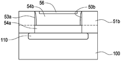
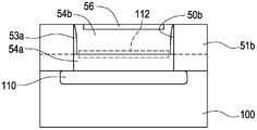
후속하여, 도 11c에서 도시된 바와 같이, Ge 또는 다양한 Ge 함량의 SiGe과 같은 감광 재료는, 시드 층으로서 기능하고 더 상세히 설명될, 제1 감광 영역(54a)을 형성하기 위해 선택적 구역 개구부(50a)를 적어도 부분적으로 채우도록 선택적으로 성장된다. 다른 구현에서는, 제1 감광 영역(54a)을 선택적으로 성장시키기 이전에, 계면 층(112)이 도 2a 내지 도 3c를 참조하여 설명된 바와 같은 반대 도핑 층으로서, 또는 도 4a 내지 도 4c를 참조하여 설명된 바와 같은 확산 제어 층으로서 형성될 수 있다.Subsequently, as shown in FIG. 11C, a photosensitive material such as Ge or SiGe of various Ge contents is deposited on the
도 11d에서 도시된 바와 같이, 패시베이션 층(53)은 필드 유전체 층(50)의 상부 표면 및 제1 감광 영역(54a)의 상부 표면 상에 퇴적된다. 패시베이션 층(53)의 재료는 Si(비정질 또는 다-결정성), 산화물, 질화물, 하이-k 유전체 또는 그들 조합을 포함할 수 있다. 도 11e에서 도시된 바와 같이, 방향성 식각은 패시베이션 층(53)의 일부분을 제거하도록 수행되고, 패시베이션 스페이서(53a)만이 선택적 구역 개구부(50a)의 측벽 상에 남는다. 도 11f에서 도시된 바와 같이, Ge과 같은 감광 재료는 제2 감광 영역(54b)을 형성하기 위해 선택적 구역 개구부(50a)의 나머지 부분을 채우도록 선택적으로 성장되고, 제2 감광 영역(54b)은 그 후 CMP 공정에 의해 평탄화된다. 마지막으로, 도 11g에서 도시된 바와 같이, 도핑된 층(56)은 제2 감광 영역(54b) 내에 그리고 제2 감광 영역(54b)의 상부 표면 가까이에 형성된다. 일부 구현에서, 도핑된 층(56)의 도핑 유형은 p-형이고, 도핑된 영역(110)의 도핑 유형은 n-형이다. 일부 구현에서, 도핑된 층(56)의 도핑 유형은 n-형이고, 도핑된 영역(110)의 도핑 유형은 p-형이다. 일부 구현에서, 도핑된 층(56)의 구역은 상부로부터 볼 때 감광 영역(54b)과는 다른 형상을 가질 수 있다. 예컨대, 감광 영역(54b)의 형상은 직사각형일 수 있고, 도핑된 층(56)의 형상은 원형일 수 있다. 일부 구현에서, 선택적 구역 개구부(50a)는 직사각형이고 (110) 평면에 의해 둘러싸이되 Ge을 포함하는 감광 영역에 의해 채워질 때 양호한 표면 패시베이션을 초래할 수 있다. 특정 실시형태에서는, (110) 이외의 다른 평면이 또한 직사각형을 형성하도록 사용될 수 있다. 접합 커패시턴스를 감축하기 위해, 도핑된 층(56)은 직사각형 개구부(50b)보다 더 작고, 입력 광학 빔 프로파일과 실질적으로 일치하도록 원형 형상일 수 있다. 일부 구현에서, 도핑된 층(56)의 구역은 상부로부터 볼 때 감광 영역(54b)과 유사한 형상을 가질 수 있다. 예컨대, 감광 영역(54b)과 도핑된 층(56)의 형상은 둘 다 직사각형 또는 원형일 수 있다. 일부 구현에서, 감광 영역(54b)과 도핑된 영역(56)의 형상은 둘 다 둥근 코너를 갖는 직사각형일 수 있다. 도 11g에서 도시된 공정 단계의 완료시, 도 2f 내지 도 2h에서 도시된 것들과 유사한 후속 공정 또는 다른 변형이 광 다이오드의 전기적 콘택트를 형성하도록 수행될 수 있다.As shown in FIG. 11D, a
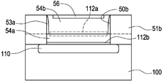
도 11h는 본 발명의 또 다른 구현에 따라 측벽 패시베이션을 갖는 광 다이오드를 도시하는 단면도이다. 도 11h에서 도시된 광 다이오드는 패시베이션 층(150)이 제2 감광 영역(54b) 및 도핑된 층(56)의 정상에 형성된다는 것을 제외하고는 도 11g에서 도시된 것과 유사하다. 도 11i는 본 발명의 또 다른 구현에 따라 측벽 패시베이션을 갖는 광 다이오드를 도시하는 단면도이다. 도 11i에서 도시된 광 다이오드는 이러한 구현에서는 계면 층(112)이 생략될 수 있다는 것을 제외하고는 도 11g에서 도시된 것과 유사하다. 도 11j는 본 발명의 또 다른 구현에 따라 측벽 패시베이션을 갖는 광 다이오드를 도시하는 단면도이다. 도 11j에서 도시된 광 다이오드는 계면 층(112)이 제1 감광 영역(54a)과 제2 감광 영역(54b)의 사이에 놓인다는 것을 제외하고는 도 11g에서 도시된 것과 유사하다. 도 11k는 본 발명의 또 다른 구현에 따라 측벽 패시베이션을 갖는 광 다이오드를 도시하는 단면도이다. 도 11k에서 도시된 광 다이오드는 이러한 구현에서는 2개의 계면 층(112a, 112b)이 채용된다는 것을 제외하고는 도 11g에서 도시된 것과 유사하다. 즉, 제1 계면 층(112a)은 제1 감광 영역(54a)과 제2 감광 영역(54b) 사이에 놓이고, 제2 제1 계면 층(112b)은 도핑된 층(110)과 제2 감광 영역(54b) 사이에 놓인다. 도 11에서, 완전 층 영역 및 파선 박스 영역의 예시는 둘 다 계면 층(112)의 존재를 표시함을 주목한다. 전술한 "Si 기판(100)의 표면"은 특정 구현에서는 "도핑된 층(110)의 표면"과 호환가능하다.11H is a cross-sectional view illustrating a photodiode with sidewall passivation in accordance with another embodiment of the present invention. The photodiode shown in Fig. 11H is similar to that shown in Fig. 11G except that the
도 12a 내지 도 12g는 본 발명의 다른 구현에 따라 측벽 패시베이션을 갖는 광 다이오드를 형성하는 제조 단계를 예시하는 단면도이다. 유사하게, 공정은 도 2a에서 도시된 단계(S100)를 계승할 수 있다. 도 12a에서, Si 기판(100)은 도핑된 층(110)을 갖고, 필드 유전체 층(51a)은 Si 기판(100)의 표면 상에 퇴적된다. 선택적 구역 개구부(50a)는 포토리소그래피 및 식각에 의해 필드 유전체 층(51a)에 획정되되, 선택적 구역 개구부(50a)는 Si 기판(100)의 표면의 일부분을 노출시켰다. 후속하여, 시드 층(54a)은 선택적 구역 개구부(50a)를 채우도록 선택적으로 성장된다. 일부 구현에서는, 제1 감광 영역(54a)을 선택적으로 성장시키기 전에, 계면 층(112)이 도 2a 내지 도 3c를 참조하여 설명된 바와 같은 반대 도핑으로서, 또는 도 4a 내지 도 4c를 참조하여 설명된 바와 같은 확산 제어로서 형성될 수 있다. 일부 구현에서는, 시드 층(54a)의 성장 후에 선택사항인 CMP 공정이 수행될 수 있다. 도 12b에서, 제2 격리 층(51b)이 퇴적되고, 제2 격리 층(51b)의 일부분은 도 12c에서 도시된 바와 같이 제2 선택된 구역(50b)을 노출시키도록 제거된다. 특정 실제 공정 구현에서는 수반된 2개의 별개의 리소그래피 단계에 기인하여 선택적 개구부(50a)와 제2 선택된 구역(50b) 간 측벽 오정렬이 존재할 수 있음을 주목한다.12A-12G are cross-sectional views illustrating fabrication steps to form a photodiode with sidewall passivation in accordance with another embodiment of the present invention. Similarly, the process can inherit step S100 shown in FIG. 2A. In Fig. 12A, the
도 12d에서는, 패시베이션 층(53)이 퇴적된다. 일부 구현에서, 패시베이션 층(53)의 재료는 Si(비정질 또는 다-결정성), 산화물, 질화물, 하이-k 유전체(예컨대, Al2O3, HfO2) 또는 그들 조합일 수 있다. 도 12e에서 도시된 바와 같이, 방향성 식각은 패시베이션 층(53)을 부분적으로 제거하도록 수행되고, 패시베이션 스페이서(53a)만이 선택적 구역 개구부(50b)의 측벽(즉, 필드 유전체 층(51b)의 내측 표면) 상에 남는다.In Fig. 12D, a
도 12f에서 도시된 바와 같이, Ge과 같은 감광 재료는 제2 감광 영역(54b)을 형성하기 위해 선택적 구역 개구부(50b)의 나머지 부분을 채우도록 선택적으로 성장되고, 제2 감광 영역(54b)은 그 후 CMP 공정에 의해 평탄화된다. 마지막으로, 도 12g에서 도시된 바와 같이, 도핑된 층(56)은 제2 감광 영역(54b) 내에 그리고 제2 감광 영역(54b)의 상부 표면 가까이에 형성된다. 일부 구현에서, 도핑된 층(56)의 도핑 유형은 P-형이고, 도핑된 영역(110)의 도핑 유형은 n-형이다. 일부 구현에서, 도핑된 층(56)의 도핑 유형은 n-형이고, 도핑된 영역(110)의 도핑 유형은 p-형이다. 일부 구현에서, 도핑된 층(56)의 구역은 상부로부터 볼 때 감광 영역(54b)과는 다른 형상을 가질 수 있다. 예컨대, 감광 영역(54b)의 형상은 직사각형일 수 있고, 도핑된 층(56)의 형상은 원형일 수 있다. 일부 구현에서, 선택적 구역 개구부(50b)는 직사각형이고 (110) 평면에 의해 둘러싸이되 Ge을 포함하는 감광 영역에 의해 채워질 때 양호한 표면 패시베이션을 초래할 수 있다. 특정 실시형태에서는, (110) 이외의 다른 평면이 또한 직사각형을 형성하도록 사용될 수 있다. 접합 커패시턴스를 감축하기 위해, 도핑된 층(56)은 직사각형 개구부(50b)보다 더 작고, 입력 광학 빔 프로파일과 실질적으로 일치하도록 원형 형상일 수 있다. 일부 구현에서, 도핑된 층(56)의 구역은 상부로부터 볼 때 감광 영역(54)과 유사한 형상을 가질 수 있다. 예컨대, 감광 영역(54)과 도핑된 층(56)의 형상은 둘 다 직사각형 또는 원형일 수 있다. 예컨대, 감광 영역(54)과 도핑된 영역(56)의 형상은 둘 다 둥근 코너를 갖는 직사각형일 수 있다. 도 12g에서 도시된 공정 단계의 완료시, 도 2f 내지 도 2h에서 도시된 것과 유사한 후속 공정 또는 다른 변형이 광 다이오드의 전기적 콘택트를 형성하도록 수행될 수 있다.As shown in Fig. 12F, a photosensitive material such as Ge is selectively grown to fill the remaining portion of the
도 12h는 본 발명의 또 다른 구현에 따라 측벽 패시베이션을 갖는 광 다이오드를 도시하는 단면도이다. 도 12h에서 도시된 광 다이오드는 패시베이션 층(150)이 제2 감광 영역(54b) 및 도핑된 층(56)의 정상에 형성된다는 것을 제외하고는 도 12g에서 도시된 것과 유사하다. 도 12i는 본 발명의 또 다른 구현에 따라 측벽 패시베이션을 갖는 광 다이오드를 도시하는 단면도이다. 도 12i에서 도시된 광 다이오드는 이러한 구현에서는 계면 층(112)이 생략될 수 있다는 것을 제외하고는 도 12g에서 도시된 것과 유사하다. 도 12j는 본 발명의 또 다른 구현에 따라 측벽 패시베이션을 갖는 광 다이오드를 도시하는 단면도이다. 도 12j에서 도시된 광 다이오드는 계면 층(112)이 제1 감광 영역(54a)과 제2 감광 영역(54b)의 사이에 놓인다는 것을 제외하고는 도 12g에서 도시된 것과 유사하다. 도 12k는 본 발명의 또 다른 구현에 따라 측벽 패시베이션을 갖는 광 다이오드를 도시하는 단면도이다. 도 12k에서 도시된 광 다이오드는 이러한 구현에서는 2개의 계면 층(112a, 112b)이 채용된다는 것을 제외하고는 도 12g에서 도시된 것과 유사하다. 즉, 제1 계면 층(112a)은 제1 감광 영역(54a)과 제2 감광 영역(54b) 사이에 놓이고, 제2 계면 층(112b)은 도핑된 층(110)과 제2 감광 영역(54b) 사이에 놓인다. 도 12에서, 완전 층 영역 및 파선 박스 영역의 예시는 둘 다 계면 층(112)의 존재를 표시함을 주목한다. 또한, 도 12에서 도시된 도면은 예시적 목적을 위한 것이고 제한적 의미로 보여서는 아니됨을 주목한다. 예컨대, 도 12d 내지 도 12k에서, 스페이서 형성은 또한 이러한 2-단계 퇴적/성장 시나리오에서 선택사항일 수 있다, 즉, 시드 영역(54a)을 우선 형성하고, 그 후 스페이서(53a)를 도입함이 없이 제2 감광 영역(54b)을 형성한다. 다른 예로서, 감광 영역(54b)의 두께는 시드 영역(54a)의 두께보다 더 얇거나 더 두꺼울 수 있고, 감광 영역(54b)용 개구부 구역은 시드 영역(54a)보다 더 크거나, 같거나, 더 작을 수 있다. 전술한 "Si 기판(100)의 표면"은 특정 실시형태에서는 "N 도핑된 층(110)의 표면"과 호환가능하다.12H is a cross-sectional view illustrating a photodiode with sidewall passivation in accordance with another embodiment of the present invention. The photodiode shown in Figure 12h is similar to that shown in Figure 12G except that the
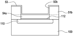
도 13은 트랜지스터와 집적된 본 발명의 광 다이오드를 도시하는 단면도이다. 고도의 도핑 영역은 트랜지스터(70)의 소스(72) 및 드레인(74) 영역에 대해 기판(100)에서 제공된다. 광 다이오드와 트랜지스터 간 격리는 얕은 트렌치 격리, P-N 접합 격리, 열 산화물 또는 다른 형태의 격리에 의해 행해질 수 있다.13 is a cross-sectional view showing a photodiode of the present invention integrated with a transistor. A highly doped region is provided in the
본 발명이 특정 예시적 실시형태를 참조하여 설명되었기는 하지만, 위에서 설명된 구현 중 전부 및 어느 것이라도 서로 조합될 수 있고, 본 발명은 설명된 구현으로 한정되지 않고, 본 발명의 취지 및 범위 내에서의 수정 및 개조로 실시될 수 있음을 인식할 것이다. 따라서, 명세서 및 도면은 제한적 의미보다는 예시적 의미로 간주되어야 한다.Although the present invention has been described with reference to specific exemplary embodiments, all and any of the implementations described above can be combined with one another, and the present invention is not limited to the described implementations, It will be appreciated that the invention may be practiced with modification and adaptation within the spirit and scope of the appended claims. Accordingly, the specification and drawings are to be regarded in an illustrative rather than a restrictive sense.
일부 구현에서, 계면 층, 시드 층 및 감광 영역의 재료는 Si, Ge, 또는 다양한 Ge 함량을 갖는 SiGe일 수 있다. 일부 구현에서, 감광 영역은 시드 층보다 더 높은 Ge 함량을 갖는다. 더욱, 계면 층은 시드 층과 기판 사이에, 또는/그리고 감광 영역과 기판 사이에, 또는/그리고 시드 층과 감광 영역 사이에 삽입될 수 있다. 일부 구현에서, 계면 층은 반대 도핑 층, 또는/그리고 도판트 확산 층, 또는/그리고 대역폭 조절 층으로서 기능할 수 있다. 일부 구현에서, 시드 층은 Si를 포함하고, 기판으로부터 감광 영역으로 도판트 확산을 감축하도록 도판트 확산 제어 층으로서 기능한다.In some implementations, the material of the interface layer, the seed layer, and the light-sensitive region may be Si, Ge, or SiGe with various Ge contents. In some implementations, the light sensitive region has a higher Ge content than the seed layer. Furthermore, an interfacial layer may be interposed between the seed layer and the substrate, and / or between the light-sensitive region and the substrate, and / or between the seed layer and the light-sensitive region. In some implementations, the interface layer may function as an opposite doping layer, and / or as a dopant diffusion layer, and / or as a bandwidth tuning layer. In some implementations, the seed layer comprises Si and functions as a dopant diffusion control layer to reduce dopant diffusion from the substrate to the photosensitive region.
일부 구현에서, 시드 층은 Ge과 같은 감광 영역과 실질적으로 동일한 재료 함량을 갖는다. 특정 실시형태에서, 실리사이드를 형성하는 것과 같은 다른 공정 단계가 2개의 성장 사이에 수행될 수 있으므로 열 처리량을 감축하도록 시드 층은 시드 층 위의 감광 영역과는 별개로 성장될 수 있다. 그러한 2-단계 성장 방법은 실질적으로 동일한 재료 조성의 감광 영역에 대한 더 높은 전반적 달성가능한 두께를 가능하게 한다. 일부 구현에서, 수반된 다수의 리소그래피 단계에 기인하여 시드 구역과 제2 선택적 구역 간 의도적 또는 의도적이지 않은 측벽 오정렬이 존재한다. 선택적 성장이 수행되는 일부 구현에서, 경사진 형상이 성장 단계 동안 형성되고, 본 개시에서 언급된 바와 같이 CMP 단계에 의해 추후 폴리싱될 수 있다. 예컨대, Ge이 표면 상에 선택적으로 에피택셜 성장되면 (311) 평면이 형성될 수 있다. 일부 구현에서는, 오목하게 된 구조가 기판 도핑 및 계면 층을 형성하기 전에 포함될 수 있다. 일부 구현에서는, 또한 앞서 설명된 스페이서 형성 공정에 따라 오목 구역의 측벽을 덮도록 스페이서가 형성될 수 있다. 특정 실제 구현 유발된 결함은 또한 그 개념이 본 개시를 따르는 한 본 개시에서 다루어져야 함을 주목한다. 위 설명으로부터의 어느 변형, 파생이라도 또한 본 발명에 포함된다고 보아야 한다.In some implementations, the seed layer has substantially the same material content as the light-sensitive region, such as Ge. In certain embodiments, other process steps, such as forming a silicide, may be performed between the two growths, so that the seed layer may be grown separately from the light sensitive region on the seed layer to reduce thermal throughput. Such a two-step growth method enables a higher overall achievable thickness for the light-sensitive area of substantially the same material composition. In some implementations, intentional or unintentional sidewall misalignment exists between the seed zone and the second selective zone due to the multiple lithography steps involved. In some implementations where selective growth is performed, a tapered shape is formed during the growth step and may be subsequently polished by a CMP step as described in this disclosure. For example, if Ge is selectively epitaxially grown on the surface (311), a plane can be formed. In some implementations, the recessed structure may be included prior to forming the substrate doping and interface layers. In some implementations, spacers may also be formed to cover the sidewalls of the recessed areas in accordance with the spacer forming process described above. It is noted that certain actual implementation-induced defects must also be addressed in this disclosure as long as the concepts are consistent with this disclosure. Any variation or derivation from the above description is to be considered as including the present invention.
본 명세서가 많은 상세를 포함하고 있기는 하지만, 이것들은 제한으로서가 아니라, 그보다는 특정 실시형태에 특정한 특징의 설명으로서 해석되어야 한다. 별개의 실시형태 또는 구현의 맥락에서 본 명세서에 설명되어 있는 특정 특징은 또한 단일 실시형태로 조합하여 구현될 수 있다. 반대로, 단일 실시형태의 맥락에서 설명되어 있는 다양한 특징은 또한 다수의 실시형태로 별개로 또는 어느 적합한 부-조합으로라도 구현될 수 있다. 더욱, 특징이 특정 조합으로 작용하는 것으로 위에서 설명되고, 심지어 최초에는 그와 같이 청구될 수 있기는 하지만, 청구된 조합으로부터의 하나 이상의 특징은 일부 경우에서는 그 조합으로부터 삭제될 수 있고, 청구된 조합은 부-조합 또는 부-조합의 변형으로 지향될 수 있다.While this specification contains many specifics, these should not be construed as limitations, but rather as a description of features that are specific to a particular embodiment. Certain features described herein in the context of separate embodiments or implementations may also be implemented in combination in a single embodiment. Conversely, various features described in the context of a single embodiment may also be implemented separately or in any suitable sub-combination in any number of embodiments. Furthermore, although one or more of the features from the claimed combination may be deleted from the combination in some cases, and the claimed combination may be removed from the combination, Sub-combination or sub-combination.
유사하게, 동작은 도면에서는 특정 순서로 묘사되어 있기는 하지만, 이것은, 바람직한 결과를 달성하기 위해, 그러한 동작이 도시된 특정 순서로 또는 순차적 순서로 수행되어야 함, 또는 모든 예시된 동작이 수행되어야 함을 필요로 하는 것으로 이해되어서는 안 된다. 특정 상황에서는, 멀티태스킹 및 병렬 처리가 유익할 수 있다. 더욱, 위에서 설명된 실시형태에서의 다양한 시스템 컴포넌트의 분리는 모든 실시형태에서 그러한 분리를 필요로 하는 것으로 이해되어서는 안 된다.Similarly, although the operations are depicted in a particular order in the figures, it should be understood that such operations must be performed in the specific order shown or in sequential order, or that all illustrated acts be performed to achieve the desired result Should not be understood as requiring. In certain situations, multitasking and parallel processing may be beneficial. Moreover, the separation of various system components in the embodiments described above should not be understood as requiring such separation in all embodiments.
그렇게, 특정 실시형태가 설명되었다. 다른 실시형태가 이하의 청구항들의 범위 내에 있다. 예컨대, 청구범위에서 나열된 동작은 다른 순서로 수행될 수 있고 역시 바람직한 결과를 달성할 수 있다.As such, certain embodiments have been described. Other embodiments are within the scope of the following claims. For example, the operations listed in the claims may be performed in a different order and may also achieve desirable results.
Claims (20)
(1) 기판 위에 격리 층을 형성하는 단계,
(2) 선택된 구역을 노출시키도록 상기 격리 층의 일부분을 제거하는 단계,
(3) 상기 선택된 구역의 측벽의 적어도 일부분을 덮는 스페이서를 형성하는 단계,
(4) 상기 선택된 구역 내에 게르마늄을 포함하는 제1 흡수 층을 에피택셜 성장시키는 단계,
(5) 상기 제1 흡수 층 위에 실리콘을 포함하는 패시베이션 층을 형성하는 단계를 포함하되,
표면 누설 전류는 상기 제1 흡수 층을 패시베이팅함으로써 감축될 수 있고, 낮은 암전류 및 높은 감도 광 흡수 장치가 형성될 수 있는,
광 흡수 장치를 형성하기 위한 방법.
A method for forming a light absorbing device,
(1) forming an isolation layer on a substrate,
(2) removing a portion of the isolation layer to expose a selected region,
(3) forming a spacer covering at least a portion of a sidewall of the selected area,
(4) epitaxially growing a first absorber layer comprising germanium in the selected zone,
(5) forming a passivation layer comprising silicon on the first absorber layer,
The surface leakage current can be reduced by passivating the first absorber layer, and a low dark current and high sensitivity light absorber can be formed,
A method for forming a light absorbing device.
단계(2) 전에, 시드 구역을 노출시키도록 상기 격리 층의 일부분을 제거하는 단계, 상기 시드 구역 내에 시드 층을 형성하는 단계, 및 다른 격리 층을 퇴적시키는 단계를 더 포함하되,
상기 시드 구역은 상기 선택된 구역과 적어도 부분적으로 겹치고 있는,
광 흡수 장치를 형성하기 위한 방법.
The method according to claim 1,
Further comprising the step of removing a portion of the isolation layer to expose the seed region prior to step (2), forming a seed layer within the seed region, and depositing another isolation layer,
Wherein the seed zone is at least partially overlapping the selected zone,
A method for forming a light absorbing device.
시드 재료를 형성하기 전에 상기 시드 구역 내에 스페이서를 형성하는 단계를 더 포함하는,
광 흡수 장치를 형성하기 위한 방법.
3. The method of claim 2,
Further comprising forming a spacer in the seed zone prior to forming the seed material,
A method for forming a light absorbing device.
상기 기판과 상기 제1 흡수 층 사이에 실리콘을 포함하는 제1 계면 층을 형성하는 단계를 더 포함하되,
상기 계면 층은 상기 제1 흡수 층에 비해 더 낮은 유전율을 갖는,
광 흡수 장치를 형성하기 위한 방법.
The method according to claim 1,
Further comprising forming a first interfacial layer comprising silicon between the substrate and the first absorbent layer,
Wherein the interface layer has a lower dielectric constant than the first absorption layer,
A method for forming a light absorbing device.
상기 시드 층과 상기 제1 흡수 층 사이에 실리콘을 포함하는 제2 계면 층을 형성하는 단계를 더 포함하되,
상기 계면 층은 상기 제1 흡수 층에 비해 더 낮은 유전율을 갖는,
광 흡수 장치를 형성하기 위한 방법.
3. The method of claim 2,
Forming a second interface layer including silicon between the seed layer and the first absorption layer,
Wherein the interface layer has a lower dielectric constant than the first absorption layer,
A method for forming a light absorbing device.
단계(4) 전에, 트랜지스터의 소스 및 드레인 영역에 대해 상기 기판에서 고도의 도핑 영역을 형성하는 단계를 더 포함하는,
광 흡수 장치를 형성하기 위한 방법.
The method according to claim 1,
Further comprising forming a highly doped region in the substrate relative to the source and drain regions of the transistor prior to step (4)
A method for forming a light absorbing device.
(1) 기판에 적어도 부분적으로 매립된 제1 도핑 영역을 형성하는 단계,
(2) 상기 제1 도핑 영역 위에 제1 층을 형성하는 단계,
(3) 상기 제1 층 위에 게르마늄을 포함하는 제2 층을 형성하는 단계,
(4) 상기 제2 층을 덮는 제3 층을 형성하는 단계,
(5) 상기 제3 층 위에 산화물을 포함하는 제4 층을 형성하는 단계,
(6) 상기 제4 층 위에 질화물을 포함하는 제5 층을 형성하는 단계,
(7) 상기 제5 층을 제거하고, 상기 제4 층 상에서 정지하는 단계,
(8) 상기 제4 층 위에 제6 층을 형성하는 단계를 포함하되,
상기 제2 층은 상기 기판의 표면과의 격자 불일치를 갖고, 상기 제6 층은 광학 신호가 지나가 상기 제6 층에 의해 반사될 때 소정 반사율이 달성될 수 있도록 소정 두께를 갖고, 상기 광학 신호의 적어도 일부분은 상기 제2 층에 의해 흡수되는,
광 흡수 장치를 형성하기 위한 방법.
A method for forming a light absorbing device,
(1) forming a first doped region at least partially buried in the substrate,
(2) forming a first layer over the first doped region,
(3) forming a second layer comprising germanium on the first layer,
(4) forming a third layer covering the second layer,
(5) forming a fourth layer comprising oxide on the third layer,
(6) forming a fifth layer comprising nitride over the fourth layer,
(7) removing the fifth layer and stopping on the fourth layer,
(8) forming a sixth layer on the fourth layer,
Wherein the second layer has a lattice mismatch with the surface of the substrate and the sixth layer has a thickness such that a predetermined reflectivity can be achieved when the optical signal passes and is reflected by the sixth layer, At least a portion of which is absorbed by the second layer,
A method for forming a light absorbing device.
상기 제3 층은 산화물, 또는 질화물, 또는 실리콘, 또는 하이-k 유전체 또는 당해 조합을 포함하는,
광 흡수 장치를 형성하기 위한 방법.
8. The method of claim 7,
The third layer may comprise an oxide, or nitride, or silicon, or a high-k dielectric, or a combination thereof.
A method for forming a light absorbing device.
단계(3) 후에, 상기 제2 층을 수 개의 단위 구역으로 분리하는 도판트를 주입하는 단계를 더 포함하는,
광 흡수 장치를 형성하기 위한 방법.
8. The method of claim 7,
Further comprising, after step (3), implanting a dopant separating said second layer into several unit areas.
A method for forming a light absorbing device.
기판,
제1 선택된 구역 상의 상기 기판 위의 광 흡수 층,
상기 광 흡수 층 위의 실리콘을 포함하는 패시베이션 층,
상기 광 흡수 층의 측벽의 적어도 일부분을 둘러싸는 스페이서,
상기 스페이서의 적어도 일부분을 둘러싸는 격리 층을 포함하되,
상기 광 흡수 장치는 높은 대역폭 및 낮은 암전류를 달성할 수 있는,
광 흡수 장치.
As a light absorbing device,
Board,
A light absorbing layer on said substrate on a first selected area,
A passivation layer including silicon on the light absorbing layer,
A spacer surrounding at least a portion of the side wall of the light absorbing layer,
And an isolation layer surrounding at least a portion of the spacer,
The light absorbing device is capable of achieving high bandwidth and low dark current,
Light absorbing device.
상기 광 흡수 층은 하부 층 및 상부 층을 더 포함하되,
상기 상부 층은 상기 하부 층보다 더 높은 게르마늄 농도를 갖는,
광 흡수 장치.
11. The method of claim 10,
Wherein the light absorbing layer further comprises a lower layer and an upper layer,
Wherein the upper layer has a higher germanium concentration than the lower layer,
Light absorbing device.
상기 기판과 상기 광 흡수 층 사이의 계면 층을 더 포함하되,
상기 계면 층은 상기 광 흡수 층보다 더 높은 실리콘 농도를 갖는,
광 흡수 장치.
11. The method of claim 10,
Further comprising an interface layer between the substrate and the light absorbing layer,
Wherein the interface layer has a higher silicon concentration than the light absorbing layer,
Light absorbing device.
실리콘을 포함하는 상기 패시베이션 층은 실리사이드 콘택트를 형성하도록 더 사용될 수 있는,
광 흡수 장치.
11. The method of claim 10,
The passivation layer comprising silicon may be further used to form a silicide contact,
Light absorbing device.
상기 광 흡수 층의 상부 표면 가까이의 원형 형상 구역을 갖는 표면 도핑 영역을 더 포함하되,
상기 원형 형상 구역은 상기 제1 선택된 구역보다 더 작고, 게르마늄을 포함하는 상기 광 흡수 층은 게르마늄의 효과적 표면 패시베이션을 위해 (110) 평면에 의해 둘러싸인 직사각형 형상을 갖는 상기 제1 선택된 구역 내에 형성되는,
광 흡수 장치.
11. The method of claim 10,
Further comprising a surface doped region having a circular shaped area near the top surface of the light absorbing layer,
Wherein the circular shaped zone is smaller than the first selected zone and the light absorbing layer comprising germanium is formed in the first selected zone having a rectangular shape surrounded by a (110) plane for effective surface passivation of germanium.
Light absorbing device.
기판,
상기 기판 위에 형성되고, 제1 개구부 내의 상부 부분 및 상기 제1 개구부와 적어도 부분적으로 겹치는 제2 개구부 내의 하부 부분을 포함하는 광 흡수 층,
상기 광 흡수 층의 상기 상부 부분 위의 실리콘을 포함하는 패시베이션 층,
상기 광 흡수 층의 상기 상부 부분의 측벽의 적어도 일부분을 둘러싸는 스페이서,
상기 광 흡수 층의 상기 하부 부분 및 상기 스페이서의 적어도 일부분을 둘러싸는 격리 층을 포함하되,
광 흡수 장치는 높은 대역폭 및 낮은 암전류를 달성할 수 있는,
광 흡수 장치.
As a light absorbing device,
Board,
A light absorbing layer formed on the substrate and including a top portion in the first opening and a bottom portion in the second opening at least partially overlapping the first opening,
A passivation layer comprising silicon on the upper portion of the light absorbing layer,
A spacer surrounding at least a portion of a sidewall of the upper portion of the light absorbing layer,
And an isolation layer surrounding at least a portion of the lower portion of the light absorbing layer and the spacer,
The light-absorbing device is capable of achieving high bandwidth and low dark current,
Light absorbing device.
상기 상부 부분은 상기 하부 부분보다 더 높은 게르마늄 농도를 갖는,
광 흡수 장치.
16. The method of claim 15,
Said upper portion having a higher germanium concentration than said lower portion,
Light absorbing device.
상기 광 흡수 층보다 더 높은 실리콘 농도를 갖는, 상기 기판과 상기 광 흡수 층 사이의 계면 층을 더 포함하되, 상기 계면 층은 암전류를 더 감축하도록 계면 표면 트랩 상태를 패시베이팅하는,
광 흡수 장치.
16. The method of claim 15,
Further comprising an interfacial layer between the substrate and the light absorbing layer, the interfacial layer having a higher silicon concentration than the light absorbing layer, wherein the interface layer passivates the interfacial surface trap state to further reduce dark current,
Light absorbing device.
실리콘을 포함하는 상기 패시베이션 층은 실리사이드 콘택트를 형성하도록 더 사용될 수 있는,
광 흡수 장치.
16. The method of claim 15,
The passivation layer comprising silicon may be further used to form a silicide contact,
Light absorbing device.
상기 광 흡수 층의 상기 하부 부분의 측벽을 둘러싸는 스페이서를 더 포함하는,
광 흡수 장치.
16. The method of claim 15,
And a spacer surrounding the side wall of the lower portion of the light absorbing layer.
Light absorbing device.
상기 광 흡수 층의 상기 상부 부분의 상부 표면 가까이의 원형 형상 구역을 갖는 표면 도핑 영역을 더 포함하되,
상기 원형 형상 구역은 상기 제1 개구부보다 더 작고, 게르마늄을 포함하는 상기 광 흡수 층은 게르마늄의 효과적 표면 패시베이션을 위해 (110) 평면에 의해 둘러싸인 직사각형 형상을 갖는 상기 제1 개구부 내에 형성되는,
광 흡수 장치.
16. The method of claim 15,
Further comprising a surface doped region having a circular shaped area near the upper surface of the upper portion of the light absorbing layer,
Wherein the circular shaped region is smaller than the first opening and the light absorbing layer comprising germanium is formed in the first opening having a rectangular shape surrounded by a (110) plane for effective surface passivation of germanium.
Light absorbing device.
Applications Claiming Priority (11)
| Application Number | Priority Date | Filing Date | Title |
|---|---|---|---|
| US201462078986P | 2014-11-13 | 2014-11-13 | |
| US62/078,986 | 2014-11-13 | ||
| US201462081574P | 2014-11-19 | 2014-11-19 | |
| US62/081,574 | 2014-11-19 | ||
| US201562121448P | 2015-02-26 | 2015-02-26 | |
| US62/121,448 | 2015-02-26 | ||
| US201562126698P | 2015-03-01 | 2015-03-01 | |
| US62/126,698 | 2015-03-01 | ||
| US201562197098P | 2015-07-26 | 2015-07-26 | |
| US62/197,098 | 2015-07-26 | ||
| PCT/US2015/060735 WO2016077791A1 (en) | 2014-11-13 | 2015-11-13 | Light absorption apparatus |
Publications (1)
| Publication Number | Publication Date |
|---|---|
| KR20170077241A true KR20170077241A (en) | 2017-07-05 |
Family
ID=55955171
Family Applications (1)
| Application Number | Title | Priority Date | Filing Date |
|---|---|---|---|
| KR1020177015424A KR20170077241A (en) | 2014-11-13 | 2015-11-13 | Light absorption apparatus |
Country Status (7)
| Country | Link |
|---|---|
| US (2) | US9748307B2 (en) |
| EP (1) | EP3218933A4 (en) |
| JP (1) | JP6302143B2 (en) |
| KR (1) | KR20170077241A (en) |
| CN (1) | CN107210308B (en) |
| TW (1) | TWI621253B (en) |
| WO (1) | WO2016077791A1 (en) |
Families Citing this family (35)
| Publication number | Priority date | Publication date | Assignee | Title |
|---|---|---|---|---|
| US10383520B2 (en) * | 2014-09-18 | 2019-08-20 | Masimo Semiconductor, Inc. | Enhanced visible near-infrared photodiode and non-invasive physiological sensor |
| US9799689B2 (en) | 2014-11-13 | 2017-10-24 | Artilux Inc. | Light absorption apparatus |
| WO2016077791A1 (en) | 2014-11-13 | 2016-05-19 | Artilux Inc. | Light absorption apparatus |
| WO2016085880A1 (en) | 2014-11-24 | 2016-06-02 | Artilux, Inc. | Monolithic integration techniques for fabricating photodetectors with transistors on same substrate |
| JP2017022175A (en) * | 2015-07-07 | 2017-01-26 | ルネサスエレクトロニクス株式会社 | Semiconductor device and manufacturing method of the same |
| TWI694604B (en) | 2015-07-23 | 2020-05-21 | 光澄科技股份有限公司 | Optical sensor |
| US10861888B2 (en) | 2015-08-04 | 2020-12-08 | Artilux, Inc. | Silicon germanium imager with photodiode in trench |
| US10707260B2 (en) | 2015-08-04 | 2020-07-07 | Artilux, Inc. | Circuit for operating a multi-gate VIS/IR photodiode |
| US10761599B2 (en) | 2015-08-04 | 2020-09-01 | Artilux, Inc. | Eye gesture tracking |
| EP3332426B1 (en) | 2015-08-04 | 2019-10-09 | Artilux Inc. | Germanium-silicon light sensing apparatus |
| CN115824395B (en) | 2015-08-27 | 2023-08-15 | 光程研创股份有限公司 | Wide-spectrum optical sensor |
| US10254389B2 (en) | 2015-11-06 | 2019-04-09 | Artilux Corporation | High-speed light sensing apparatus |
| US10886309B2 (en) | 2015-11-06 | 2021-01-05 | Artilux, Inc. | High-speed light sensing apparatus II |
| US10739443B2 (en) | 2015-11-06 | 2020-08-11 | Artilux, Inc. | High-speed light sensing apparatus II |
| US10418407B2 (en) | 2015-11-06 | 2019-09-17 | Artilux, Inc. | High-speed light sensing apparatus III |
| US10741598B2 (en) | 2015-11-06 | 2020-08-11 | Atrilux, Inc. | High-speed light sensing apparatus II |
| US10147829B2 (en) | 2016-09-23 | 2018-12-04 | Taiwan Semiconductor Manufacturing Co., Ltd. | Dielectric sidewall structure for quality improvement in Ge and SiGe devices |
| FR3061354B1 (en) * | 2016-12-22 | 2021-06-11 | Commissariat Energie Atomique | COMPONENT REALIZATION PROCESS INCLUDING III-V MATERIALS AND COMPATIBLE SILICON INDUSTRY CONTACTS |
| TWI741157B (en) * | 2017-02-28 | 2021-10-01 | 美商光程研創股份有限公司 | High-speed light sensing apparatus ii |
| TWI767862B (en) * | 2017-04-13 | 2022-06-11 | 美商光程研創股份有限公司 | Circuit coupled to photodetector |
| US11482553B2 (en) | 2018-02-23 | 2022-10-25 | Artilux, Inc. | Photo-detecting apparatus with subpixels |
| JP6975341B2 (en) | 2018-02-23 | 2021-12-01 | アーティラックス・インコーポレイテッド | Photodetector and its light detection method |
| US11105928B2 (en) | 2018-02-23 | 2021-08-31 | Artilux, Inc. | Light-sensing apparatus and light-sensing method thereof |
| CN114335030A (en) | 2018-04-08 | 2022-04-12 | 奥特逻科公司 | Optical detection device |
| FR3080948A1 (en) | 2018-05-02 | 2019-11-08 | Stmicroelectronics (Rousset) Sas | INTEGRATED CIRCUIT COMPRISING A CAPACITIVE ELEMENT, AND MANUFACTURING METHOD |
| US10854770B2 (en) | 2018-05-07 | 2020-12-01 | Artilux, Inc. | Avalanche photo-transistor |
| US10969877B2 (en) | 2018-05-08 | 2021-04-06 | Artilux, Inc. | Display apparatus |
| US11114489B2 (en) * | 2018-06-18 | 2021-09-07 | Kla-Tencor Corporation | Back-illuminated sensor and a method of manufacturing a sensor |
| US11574942B2 (en) | 2018-12-12 | 2023-02-07 | Artilux, Inc. | Semiconductor device with low dark noise |
| US11448830B2 (en) | 2018-12-12 | 2022-09-20 | Artilux, Inc. | Photo-detecting apparatus with multi-reset mechanism |
| TW202104927A (en) | 2019-06-19 | 2021-02-01 | 美商光程研創股份有限公司 | Photo-detecting apparatus and current reuse method |
| JP7310010B2 (en) | 2019-08-28 | 2023-07-18 | アーティラックス・インコーポレイテッド | Photodetector with low dark current |
| US20210391370A1 (en) * | 2019-08-28 | 2021-12-16 | Artilux, Inc. | Photo-detecting apparatus with low dark current |
| CN110943145B (en) * | 2019-12-13 | 2022-03-25 | 京东方科技集团股份有限公司 | Photodiode, preparation method, display substrate and display device |
| US11777043B1 (en) | 2022-06-21 | 2023-10-03 | Globalfoundries U.S. Inc. | Photodetectors with substrate extensions adjacent photodiodes |
Family Cites Families (41)
| Publication number | Priority date | Publication date | Assignee | Title |
|---|---|---|---|---|
| JPS61187267A (en) | 1985-02-14 | 1986-08-20 | Matsushita Electric Ind Co Ltd | Solid-state image pickup device |
| JPH04125977A (en) * | 1990-09-17 | 1992-04-27 | Nec Corp | Heteromultiple structure avalanche photodiode |
| JPH06132558A (en) * | 1992-10-16 | 1994-05-13 | Mitsubishi Electric Corp | Infrared detector |
| JPH09307133A (en) * | 1996-05-10 | 1997-11-28 | Victor Co Of Japan Ltd | Photodiode and its manufacture |
| JP2001284630A (en) | 2000-03-29 | 2001-10-12 | Minolta Co Ltd | Semiconductor photoelectric converter element, its use method and manufacturing method |
| JP2003163361A (en) * | 2001-11-29 | 2003-06-06 | Mitsubishi Electric Corp | Photodetecting element and optical communication device |
| US7348607B2 (en) | 2002-02-01 | 2008-03-25 | Picometrix, Llc | Planar avalanche photodiode |
| US7022544B2 (en) | 2002-12-18 | 2006-04-04 | International Business Machines Corporation | High speed photodiode with a barrier layer for blocking or eliminating slow photonic carriers and method for forming same |
| US7012314B2 (en) * | 2002-12-18 | 2006-03-14 | Agere Systems Inc. | Semiconductor devices with reduced active region defects and unique contacting schemes |
| EP1620899B1 (en) | 2003-05-02 | 2014-03-12 | Picometrix, LLC | Pin photodetector |
| US7148463B2 (en) * | 2003-07-16 | 2006-12-12 | Triquint Semiconductor, Inc. | Increased responsivity photodetector |
| US8093633B2 (en) | 2004-02-17 | 2012-01-10 | Nanyang Technological University | Method and device for wavelength-sensitive photo-sensing |
| WO2006046276A1 (en) | 2004-10-25 | 2006-05-04 | Mitsubishi Denki Kabushiki Kaisha | Avalanche photodiode |
| US20060157806A1 (en) | 2005-01-18 | 2006-07-20 | Omnivision Technologies, Inc. | Multilayered semiconductor susbtrate and image sensor formed thereon for improved infrared response |
| US7220632B2 (en) | 2005-02-24 | 2007-05-22 | Freescale Semiconductor, Inc. | Method of forming a semiconductor device and an optical device and structure thereof |
| US20070262296A1 (en) * | 2006-05-11 | 2007-11-15 | Matthias Bauer | Photodetectors employing germanium layers |
| US7683397B2 (en) * | 2006-07-20 | 2010-03-23 | Intel Corporation | Semi-planar avalanche photodiode |
| US7651880B2 (en) * | 2006-11-04 | 2010-01-26 | Sharp Laboratories Of America, Inc. | Ge short wavelength infrared imager |
| JP5400280B2 (en) * | 2007-06-07 | 2014-01-29 | パナソニック株式会社 | Solid-state imaging device |
| US20110084308A1 (en) * | 2007-08-08 | 2011-04-14 | Ter-Hoe Loh | Semiconductor arrangement and a method for manufacturing the same |
| US7795064B2 (en) | 2007-11-14 | 2010-09-14 | Jds Uniphase Corporation | Front-illuminated avalanche photodiode |
| JP5522503B2 (en) * | 2008-07-28 | 2014-06-18 | 国立大学法人 東京大学 | Optical semiconductor device, photoelectric conversion device, and light modulation device |
| US8253211B2 (en) | 2008-09-24 | 2012-08-28 | Taiwan Semiconductor Manufacturing Company, Ltd. | Semiconductor sensor structures with reduced dislocation defect densities |
| KR101106480B1 (en) | 2009-06-12 | 2012-01-20 | 한국철강 주식회사 | Method for Manufacturing Photovoltaic Device |
| US8278741B2 (en) | 2009-06-30 | 2012-10-02 | Intel Corporation | Sidewall photodetector |
| JP5414415B2 (en) * | 2009-08-06 | 2014-02-12 | 株式会社日立製作所 | Semiconductor light receiving element and manufacturing method thereof |
| TWI528532B (en) | 2009-08-17 | 2016-04-01 | 聯華電子股份有限公司 | Semiconductor photodetector structure and the fabrication method thereof |
| JP5405545B2 (en) * | 2011-09-13 | 2014-02-05 | シャープ株式会社 | Photoelectric conversion element |
| KR20130052986A (en) * | 2011-11-14 | 2013-05-23 | 삼성전자주식회사 | Unit pixel of three dimensional image sensor and three dimensional image sensor including the same |
| US9171996B2 (en) * | 2012-08-20 | 2015-10-27 | Electronics And Telecommunications Research Institute | Low-voltage high-gain high-speed germanium photo detector and method of fabricating the same |
| US8872294B2 (en) | 2012-08-21 | 2014-10-28 | Micron Technology, Inc. | Method and apparatus for reducing signal loss in a photo detector |
| US20140077210A1 (en) * | 2012-09-20 | 2014-03-20 | International Business Machines Corporation | Amorphous silicon photodetector with low dark current |
| SG2013075379A (en) * | 2012-10-08 | 2014-05-29 | Agency Science Tech & Res | P-i-n photodiode |
| US20140159183A1 (en) | 2012-12-10 | 2014-06-12 | National Tsing Hua University | High-efficiency bandwidth product germanium photodetector |
| JP2014127545A (en) * | 2012-12-26 | 2014-07-07 | Sony Corp | Solid-state imaging element and solid-state imaging device including the same |
| US9614026B2 (en) * | 2013-03-13 | 2017-04-04 | The United States Of America As Represented By The Administrator Of The National Aeronautics And Space Administration | High mobility transport layer structures for rhombohedral Si/Ge/SiGe devices |
| US9698296B2 (en) * | 2013-07-08 | 2017-07-04 | Sifotonics Technologies Co., Ltd. | Compensated photonic device structure and fabrication method thereof |
| US9876127B2 (en) | 2013-11-22 | 2018-01-23 | Taiwan Semiconductor Manufacturing Company, Ltd. | Backside-illuminated photodetector structure and method of making the same |
| JP2015144163A (en) * | 2014-01-31 | 2015-08-06 | 技術研究組合光電子融合基盤技術研究所 | SiGe photodiode |
| WO2016077791A1 (en) | 2014-11-13 | 2016-05-19 | Artilux Inc. | Light absorption apparatus |
| US9799689B2 (en) | 2014-11-13 | 2017-10-24 | Artilux Inc. | Light absorption apparatus |
-
2015
- 2015-11-13 WO PCT/US2015/060735 patent/WO2016077791A1/en active Application Filing
- 2015-11-13 US US14/940,572 patent/US9748307B2/en active Active
- 2015-11-13 KR KR1020177015424A patent/KR20170077241A/en active Search and Examination
- 2015-11-13 TW TW104137635A patent/TWI621253B/en active
- 2015-11-13 CN CN201580060584.4A patent/CN107210308B/en active Active
- 2015-11-13 JP JP2017530346A patent/JP6302143B2/en active Active
- 2015-11-13 EP EP15858667.7A patent/EP3218933A4/en active Pending
-
2017
- 2017-07-17 US US15/652,187 patent/US10128303B2/en active Active
Also Published As
| Publication number | Publication date |
|---|---|
| US10128303B2 (en) | 2018-11-13 |
| CN107210308B (en) | 2018-06-29 |
| CN107210308A (en) | 2017-09-26 |
| JP6302143B2 (en) | 2018-03-28 |
| EP3218933A4 (en) | 2018-07-11 |
| TW201633517A (en) | 2016-09-16 |
| JP2017534182A (en) | 2017-11-16 |
| US9748307B2 (en) | 2017-08-29 |
| US20160141329A1 (en) | 2016-05-19 |
| TWI621253B (en) | 2018-04-11 |
| WO2016077791A1 (en) | 2016-05-19 |
| EP3218933A1 (en) | 2017-09-20 |
| US20170317135A1 (en) | 2017-11-02 |
| WO2016077791A8 (en) | 2016-12-01 |
Similar Documents
| Publication | Publication Date | Title |
|---|---|---|
| US10128303B2 (en) | Light absorption apparatus | |
| US10861884B2 (en) | Light absorption apparatus | |
| US11393940B2 (en) | Photodetector and method for forming the same | |
| EP3224866B1 (en) | Monolithic integration techniques for fabricating photodetectors with transistors on same substrate | |
| US8399949B2 (en) | Photonic systems and methods of forming photonic systems | |
| US9356163B1 (en) | Structure and method of integrating waveguides, photodetectors and logic devices | |
| US9748098B2 (en) | Controlled confined lateral III-V epitaxy | |
| US20170373064A1 (en) | Heterogeneously integrated semiconductor device and manucacturing method thereof | |
| US9412744B1 (en) | III-V CMOS integration on silicon substrate via embedded germanium-containing layer | |
| US11749763B2 (en) | Dielectric sidewall structure for quality improvement in Ge and SiGe devices | |
| CN112186075B (en) | Waveguide type photoelectric detector and manufacturing method thereof | |
| TW202230823A (en) | Optoelectronic device and method of forming the same | |
| CN115050764A (en) | Photodetector for broadband signals |
Legal Events
| Date | Code | Title | Description |
|---|---|---|---|
| A201 | Request for examination | ||
| A302 | Request for accelerated examination | ||
| AMND | Amendment | ||
| E902 | Notification of reason for refusal | ||
| AMND | Amendment | ||
| E902 | Notification of reason for refusal | ||
| AMND | Amendment | ||
| E601 | Decision to refuse application | ||
| AMND | Amendment | ||
| J201 | Request for trial against refusal decision | ||
| J301 | Trial decision |
Free format text: TRIAL NUMBER: 2018101003735; TRIAL DECISION FOR APPEAL AGAINST DECISION TO DECLINE REFUSAL REQUESTED 20180907 Effective date: 20190110 |