EP1681712A1 - Method of producing substrates for optoelectronic applications - Google Patents
Method of producing substrates for optoelectronic applications Download PDFInfo
- Publication number
- EP1681712A1 EP1681712A1 EP05290082A EP05290082A EP1681712A1 EP 1681712 A1 EP1681712 A1 EP 1681712A1 EP 05290082 A EP05290082 A EP 05290082A EP 05290082 A EP05290082 A EP 05290082A EP 1681712 A1 EP1681712 A1 EP 1681712A1
- Authority
- EP
- European Patent Office
- Prior art keywords
- substrate
- layer
- auxiliary
- carrier
- nitride
- Prior art date
- Legal status (The legal status is an assumption and is not a legal conclusion. Google has not performed a legal analysis and makes no representation as to the accuracy of the status listed.)
- Ceased
Links
Images


Classifications
-
- H—ELECTRICITY
- H10—SEMICONDUCTOR DEVICES; ELECTRIC SOLID-STATE DEVICES NOT OTHERWISE PROVIDED FOR
- H10F—INORGANIC SEMICONDUCTOR DEVICES SENSITIVE TO INFRARED RADIATION, LIGHT, ELECTROMAGNETIC RADIATION OF SHORTER WAVELENGTH OR CORPUSCULAR RADIATION
- H10F71/00—Manufacture or treatment of devices covered by this subclass
- H10F71/139—Manufacture or treatment of devices covered by this subclass using temporary substrates
-
- H—ELECTRICITY
- H10—SEMICONDUCTOR DEVICES; ELECTRIC SOLID-STATE DEVICES NOT OTHERWISE PROVIDED FOR
- H10P—GENERIC PROCESSES OR APPARATUS FOR THE MANUFACTURE OR TREATMENT OF DEVICES COVERED BY CLASS H10
- H10P90/00—Preparation of wafers not covered by a single main group of this subclass, e.g. wafer reinforcement
- H10P90/19—Preparing inhomogeneous wafers
- H10P90/1904—Preparing vertically inhomogeneous wafers
- H10P90/1906—Preparing SOI wafers
- H10P90/1914—Preparing SOI wafers using bonding
-
- H—ELECTRICITY
- H10—SEMICONDUCTOR DEVICES; ELECTRIC SOLID-STATE DEVICES NOT OTHERWISE PROVIDED FOR
- H10P—GENERIC PROCESSES OR APPARATUS FOR THE MANUFACTURE OR TREATMENT OF DEVICES COVERED BY CLASS H10
- H10P90/00—Preparation of wafers not covered by a single main group of this subclass, e.g. wafer reinforcement
- H10P90/19—Preparing inhomogeneous wafers
- H10P90/1904—Preparing vertically inhomogeneous wafers
- H10P90/1906—Preparing SOI wafers
- H10P90/1914—Preparing SOI wafers using bonding
- H10P90/1916—Preparing SOI wafers using bonding with separation or delamination along an ion implanted layer, e.g. Smart-cut
-
- H—ELECTRICITY
- H10—SEMICONDUCTOR DEVICES; ELECTRIC SOLID-STATE DEVICES NOT OTHERWISE PROVIDED FOR
- H10W—GENERIC PACKAGES, INTERCONNECTIONS, CONNECTORS OR OTHER CONSTRUCTIONAL DETAILS OF DEVICES COVERED BY CLASS H10
- H10W10/00—Isolation regions in semiconductor bodies between components of integrated devices
- H10W10/10—Isolation regions comprising dielectric materials
- H10W10/181—Semiconductor-on-insulator [SOI] isolation regions, e.g. buried oxide regions of SOI wafers
-
- H—ELECTRICITY
- H10—SEMICONDUCTOR DEVICES; ELECTRIC SOLID-STATE DEVICES NOT OTHERWISE PROVIDED FOR
- H10H—INORGANIC LIGHT-EMITTING SEMICONDUCTOR DEVICES HAVING POTENTIAL BARRIERS
- H10H20/00—Individual inorganic light-emitting semiconductor devices having potential barriers, e.g. light-emitting diodes [LED]
- H10H20/01—Manufacture or treatment
- H10H20/011—Manufacture or treatment of bodies, e.g. forming semiconductor layers
- H10H20/018—Bonding of wafers
-
- Y—GENERAL TAGGING OF NEW TECHNOLOGICAL DEVELOPMENTS; GENERAL TAGGING OF CROSS-SECTIONAL TECHNOLOGIES SPANNING OVER SEVERAL SECTIONS OF THE IPC; TECHNICAL SUBJECTS COVERED BY FORMER USPC CROSS-REFERENCE ART COLLECTIONS [XRACs] AND DIGESTS
- Y02—TECHNOLOGIES OR APPLICATIONS FOR MITIGATION OR ADAPTATION AGAINST CLIMATE CHANGE
- Y02E—REDUCTION OF GREENHOUSE GAS [GHG] EMISSIONS, RELATED TO ENERGY GENERATION, TRANSMISSION OR DISTRIBUTION
- Y02E10/00—Energy generation through renewable energy sources
- Y02E10/50—Photovoltaic [PV] energy
Definitions
- the present invention relates to a method of producing a substrate for an optoelectronic application, the substrate having at least one active nitride layer on a final carrier and a metallic intermediate layer therebetween, wherein the method comprises: preparing of an auxiliary substrate wherein one semi-conducting nitride layer is placed on an auxiliary carrier; metallising the auxiliary substrate on the side of the nitride layer; bonding of the metallised carrier substrate with the final carrier; and removing of the auxiliary carrier after the bonding step.
- GaN based light emitting devices including light emitting diodes (LEDs) and laser diodes attracted great attention in recent years. Because these devices are capable of the generation of short wavelength emissions in UV and blue regions that can have many practical applications such as high density storage, high speed data processing, solid state lighting, flat panel colour display, and quantum computing.
- LEDs light emitting diodes
- quantum computing quantum computing.
- the realisation of GaN based layers is relatively recent in comparison to GaAs based layers. Therefore, the technology of GaN based layers is still in the development stage, and many technical issues remain to be addressed and resolved before those applications can be realised.
- GaN-on-sapphire templates for blue LED mass production.
- a GaN nucleation layer is grown on a sapphire substrate.
- a two to four microns thick GaN buffer layer is grown on the nucleation layer. This growth step is very time-consuming and takes typically from two to four hours.
- an InGaN/AlGaN/GaN-LED structure including cladding layers, multiple quantum valves and p-type layers with a total thickness of the LED structure of about 1 ⁇ m is grown on the GaN buffer layer.
- the resulting structures have some disadvantages. While the sapphire substrate is less expensive, and a more popular choice than a high cost GaN-substrate, it is non-conductive, requiring two wire bonds on top of each chip. With the electrical current travelling laterally between these two contacts the packaging efficiency is greatly reduced. While sapphire is transparent, enabling more light to escape from the chip, it unfortunately acts as a thermal insulator that traps heat, dramatically reducing the high operating current efficiency and ultimately limiting the available applications.
- the GaN device structures grown on a sapphire substrate are known to have many defects that tend to effect the device performance.
- Other factors such as the insulating property and non-cleavage of sapphire material make manufacture of a GaN light emitting device with the conventional technology difficult.
- SiC substrates can be used to grow thereon a GaN-layer.
- SiC traps a substantial portion of the light being emitted since massive absorption occurs only in the UV range.
- a sapphire substrate is used as the initial GaN growth substrate followed by bonding a thermally and electrically conductive metal layer on top of the GaN.
- the sapphire substrate is lifted off the GaN, leaving it and the reflective base ready for the fabrication of vertical devices.
- the object is solved by a method of the above mentioned type wherein the step of preparing the auxiliary substrate comprises: detaching a part from a massive semi-conducting nitride substrate; and transferring said part onto the auxiliary carrier to form the semi-conducting nitride layer thereon.
- substrates for optoelectronic applications having active layer(s) with a low density of crystalline defects can be fabricated.
- the dislocation density of the active layer(s) can be brought to below 10 8 /cm 2 although the active layer(s) can be made with a low thickness. This has the effect that optoelectronic devices fabricated by using these substrates can achieve a high efficiency and lifetime at low dimensions and weight.
- the intermediate metal layer can assure good electrical conduction between the active nitride layer(s) and the carrier substrate and can serve an additional purpose as a thermal drain between the active layer(s) and the carrier substrate. This way, the final substrate can be well electrically contacted and the thermal stress during operation can be kept to a low value.
- the semi-conducting nitride substrate is a GaN-substrate or an AIN substrate.
- GaN and AIN have the advantage that the growth of these materials as well as their properties are relatively well known so that these materials can be provided with a high crystal quality.
- the massive semi-conducting nitride substrate is produced with a dislocation density of less than 10 6 /cm 2 . Because of the very low dislocation density of the semi-conducting nitride substrate from which the semi-conducting nitride layer is detached, the nitride layer formed on the auxiliary carrier has also a very low dislocation density resulting in a low dislocation density of layer(s) grown subsequently on the transferred semi-conducting nitride layer. With this method, the active part of the resulting substrate has a very good crystallinity independent from the properties of the final carrier.
- the step of detaching and transferring comprises: depositing of a dielectric layer on the semi-conducting nitride substrate; implanting species through the dielectric layer into a certain depth of the nitride substrate to form therein a predetermined splitting area; bonding of the nitride substrate on the implanted side with the auxiliary carrier; and thermal and/or mechanical treating of the nitride substrate to split said substrate along the predetermined splitting area.
- the auxiliary carrier is a substrate selected from a group of materials comprising silicon, GaAs and ZnO. These substrates can provide a high mechanical strength which is explicitly favourable during the step of detaching and transferring in which the auxiliary carrier is under relatively high mechanical stress. Furthermore, the coefficient of thermal dilatation of GaAs and ZnO is slightly higher than the coefficient of thermal dilatation of typical semi-conducting nitride layers such as GaN or AIN, resulting in an active layer of the final substrate having only slight compression which prevents occurrence of cracking effects in the active layer.
- the auxiliary substrate is annealed after the detaching and transferring step.
- the annealing step reinforces connection at the interface between the transferred nitride layer and the auxiliary carrier.
- a protective layer is brought onto the transferred nitride layer before the annealing step and is removed thereafter. This way, the transferred nitride layer can be protected from chemical influences in the annealing environment which could otherwise lead to chemical reaction(s) with the nitride layer or to other unintentional changes of crystallinity or purity of the nitride layer.
- the surface of the transferred nitride layer is smoothed after the detaching and transferring step or after the annealing step.
- the removal of a certain degree of roughness of the transferred nitride layer surface is favourable for its utilisation as a basis for subsequent layers which can be better deposited on a smooth subsurface.
- This smoothing step can be implemented before or after the annealing step.
- the additional epitaxial layer(s) are well suited to form the active layer(s) of an optoelectronic structure.
- the metallic intermediate layer is deposited on the at least one epitaxial nitride layer.
- the metallic intermediate layer can form an Ohmic contact for the at least one epitaxial nitride layer.
- the method further comprises providing a final carrier and bonding of said final carrier on the metallised side of the auxiliary substrate.
- the final carrier provides a good mechanical support for the transferred nitride layer and the deposited at least one epitaxial layer from the side opposite to the auxiliary carrier.
- the material of the final carrier is selected from a group comprising silicon, silicon carbide and copper. These materials provide good electrical and thermal conductivity which is particularly relevant for a later optoelectronic application of the produced substrate wherein the electrical conductivity can be used to form an Ohmic contact on the final carrier and the thermal conductivity serves to provide a good thermal drainage for an optoelectronic device with the final carrier.
- At least one reflection layer is deposited onto the final carrier before the bonding step of the final carrier with the auxiliary substrate.
- the reflection layer serves as a mirror between the active layer(s) and the final carrier so that the light emitted from the active layer(s) will not be absorbed by the final carrier.
- the auxiliary carrier is removed mechanically and/or chemically after the bonding step, wherein the nitride layer is used as a stop layer for the removal step.
- the active layer(s) of the final substrate can be excavated.
- the transferred nitride layer is removed from the substrate after the removal step of the auxiliary carrier.
- the removal of non-essential layer(s), such as the transferred nitride layer improves the efficiency of the whole structure since non-essential layer(s) would lead to an unwanted absorption of photons emitted from the active layer(s).
- an efficient method of producing substrates for optoelectronic applications is provided which may be used to fabricate optoelectronic devices such as LED structures or laser diodes.
- FIGS. 1 to 16 show an illustrative process flow of an embodiment of the present invention.
- the massive semi-conducting nitride substrate is a GaN-substrate 8 having a nitrogen face 18 on top and on its bottom a gallium face 19.
- the massive GaN-substrate has a hexagonal crystal structure with a dislocation density of lower than 10 6 /cm 2 .
- the planarity of the substrate 8 is in the range of 20 ⁇ m.
- the nitride substrate 8 has a thickness of about 150 to 750 ⁇ m.
- the nitrogen face 18 of the nitride substrate 8 is polished and has a surface roughness of lower than 0.3 nm RMS measured with an atomic force microscope (AFM) over a field of some 1x1 ⁇ m 2 .
- AFM atomic force microscope
- the above described technology can also be realised using a semi-conducting nitride substrate of GaN with a cubic crystal structure or with a cubic or hexagonal monocrystalline AIN substrate instead of the hexagonal GaN-substrate 8.
- the dislocation density of the substrate 8 should be between 10 5 to 10 6 /cm 2 or even lower.
- Figure 2 schematically shows a deposition step of a dielectric layer 9 on the massive semi-conducting nitride substrate 8. This deposition step is performed on the nitrogen face 18 of the nitride substrate 8.
- the dielectric layer 9 can be a material selected from a group comprising silicon dioxide, silicon nitride, a combination of these materials or other dielectric materials which have a good adhesion to the nitrogen face 18 of the GaN-substrate 8.
- the dielectric layer(s) 9 are favourably deposited by chemical vapour deposition.
- the structure shown in Figure 2 can be thermally annealed to densify the dielectric layer(s) 9.
- the structure shown in Figure 2 is implanted with species 10 in an implantation step.
- the species 10 can be of hydrogen, helium or other elements alone or in combination.
- the species 10 are implanted with energies between 20 and 200 keV and with doses between 10 15 and 10 18 at/cm 2 .
- the species 10 are implanted in a certain depth d of the nitride substrate 8 forming there a predetermined splitting area 11, at and around the implantation depth d.
- the implanted structure of Figure 3 is bonded on its implanted side with an auxiliary carrier 6.
- the auxiliary carrier 6 is preferably a silicon substrate, GaAs substrate or a ZnO substrate but can also be of another material which has relatively high mechanical stability since this material will be highly stressed during a following Smart CutTM process in which the nitride substrate 8 is split.
- the thermal dilatation coefficient of the auxiliary carrier 6 is chosen or adapted in such a way that it is slowly higher than the thermal dilatation coefficient of GaN, resulting in a structure having a GaN-layer with a slight compression preventing an appearance of cracking in this layer.
- the structure of Figure 4 is split into two parts with thermal and/or mechanical treatment.
- the stress applied due to that treatment leads to the splitting of the structure of Figure 4 along the predetermined splitting area 11.
- the splitting step results in two structures, a residual part of the former semi-conductive nitride substrate 8 and an auxiliary substrate 5 consisting of the auxiliary carrier 6, the dielectric layer 9 and a semi-conducting nitride layer 2 being a part of the former semi-conducting nitride substrate 8.
- the split structures have split surfaces 14 and 22 with an increased roughness after the splitting step.
- the auxiliary substrate 5 is smoothed in a polishing step applied on the split surface 14 of the nitride layer 2. After this polishing step, the surface roughness of the GaN-layer 2 is of an atomic level which is only several Angstroms when measured with an AFM.
- a protective layer 13 is deposited on the surface 14 of the GaN-layer 2.
- the protective layer 13 is preferably a dielectric layer.
- the structure of Figure 7 is thermally annealed in an annealing equipment 20.
- the structure is thermally treated in a temperature region between 500 and 1100 °C in a gaseous atmosphere which permits preservation of the crystal quality of the GaN-layer 2.
- the annealing step shown in Figure 8 can also be applied before the polishing step shown in Figure 6 and can also be applied directly onto the auxiliary substrate 5 without the deposition of the protective layer 13 before the annealing step.
- the thermal annealing step leads to an enforcement of the bonding forces at the interface between the auxiliary carrier 6 and the dielectric layer 9.
- the protective layer 13 which can be deposited before the annealing step shown in Figure 8, is removed in a removal step.
- the protective layer 13 can be removed with a chemical treatment, for instance with HF.
- the removal step results in the auxiliary substrate 5 having a smooth and clean gallium face 14 on top of the GaN-layer 2.
- the GaN-layer 2 is monocrystalline with a crystal quality equivalent to the crystal quality of the massive semi-conducting nitride substrate 8 as shown in Figure 1.
- the surface of the GaN-layer 2 is nearly free from particles.
- the thickness of the GaN-layer 2 is, in one favourable example of the invention, about 200nm.
- an epitaxial layer 15 is deposited on the gallium face 14 of the GaN-layer 2.
- the epitaxial layer 15 can be deposited with a known epitaxy method like MOCVD, MBE or HVPE.
- the temperature applied during the epitaxial deposition step is in the range between 700 and 1100°C.
- the epitaxial layer(s) deposited in the step shown in Figure 10 can be: of n-type GaN doped with Si and having a thickness of about 0.2 ⁇ m, of InGaN, of AlGaN and/or of p-type GaN doped with Mg.
- the total thickness of the epitaxial layer(s) 15 is, in a favourable example of the invention, about 0.5 ⁇ m.
- the composition of the epitaxial layer(s) depends on the efficiency and the wavelength of the optoelectronic structure which shall be fabricated with the resulting substrate.
- the dislocation density of the epitaxial layer(s) 15 is nearly equivalent to the dislocation density of the original GaN-substrate 8, that means lower than 10 6 /cm 2 . It is generally advantageous to have epitaxial layer(s) with an increased thickness to advance current propagation in the active layer(s) of the resulting structure.
- a metal layer 4 is deposited on the epitaxial layer(s) 15.
- the metal layer 4 serves later as an Ohmic contact to contact the resulting structure electrically.
- the metal layer 4 can be of Ni/Au, Pt, rhodium or another conductive material.
- a final carrier 7 is provided on which a reflection layer 17 is deposited.
- the final carrier 7 serves as a support substrate which is electrically conductive with a low electrical resistivity and a good thermal conductivity.
- the final carrier 7 can be of silicon, SiC, copper or another conductive or semi-conducting material.
- the reflection layer 17 can be for instance of gold, aluminium or silver which materials have good reflectivity.
- the reflection layer 17 acts later as a mirror layer arranged between the final carrier 7 and the epitaxial layer(s) 15. Said mirror is chosen depending on the emitted wavelength(s) of the resulting structure.
- the structures of Figures 11 and 12 are connected on the metal layer 4 and the reflection layer 17 in a bonding step.
- the bonding step leads to a molecular adhesion between the structures of Figures 11 and 12 to provide a contact therebetween using mechanical pressure and a certain temperature.
- the auxiliary carrier 6 and the dielectric layer 9 are removed from the bonded structure in a removal step.
- the removal step can comprise mechanical lapping and/or polishing as well as a chemical attack using the gallium nitride layer 2 as an etch stop layer.
- the removal can be realised using mechanical treatment followed by chemical treatment based on a TMAH or HF/HNO3 solution.
- Said chemical attack can be realised by immersing the structure in a bath of said solution using an equipment with which the structure can be held in rotation and in which the auxiliary carrier can be exposed to the chemical solution.
- the removal of the auxiliary carrier can also be realised by using only chemical treatment.
- the gallium nitride layer 2 is removed from the structure shown in Figure 14.
- a removal of non-doped GaN-layer 2 can result in an enhancement of efficiency of the resulting structure since such layers would only lead to an unfortunate absorption of photons.
- GaN absorbs, for instance, UV radiation.
- an electrical contact 21 is provided on the epitaxial layer(s) 15.
- the resulting structure consists of the final carrier 7, the reflection layer 17, the metal layer 4, the epitaxial layer(s) 15 and the electrical contact 21.
- the metal layer 4 and the reflection layer 17 form together a metallic junction or metallic intermediate layer between the carrier substrate 7 and the epitaxial layer(s) 15.
- the metallic intermediate layer can include or not include the reflection layer 17.
- the structure shown in Figure 16 is further processed by using lithographic and etch steps for chip fabrication, deposition steps of dielectric layers for preservation of the structure and deposition steps of metal layers to realise contacts on both sides of the structure.
- the fabricated structures are separated into chips which are packaged finally.
- a substrate with an active layer of very good crystal quality and with eliminated non-electronic applications can be realised for optoelectronic applications.
- the good crystal quality is very important for a high efficiency and long life span of the structures, in particular for LED structures of laser diodes.
- Due to the elimination of GaN non layers in the inventive method allows minimisation of photon absorption in the active layer(s) resulting in a high efficiency of light radiation.
- the inventive technology uses the very good crystallinity of the massive nitride substrate in a direct transfer of a part of said substrate to the final substrate. This way, the final active epitaxial layer(s) can be grown directly on the high quality transferred part with the same good crystallinity leading to high quality final structures.
Landscapes
- Led Devices (AREA)
- Semiconductor Lasers (AREA)
- Recrystallisation Techniques (AREA)
- Crystals, And After-Treatments Of Crystals (AREA)
Abstract
Description
- The present invention relates to a method of producing a substrate for an optoelectronic application, the substrate having at least one active nitride layer on a final carrier and a metallic intermediate layer therebetween, wherein the method comprises: preparing of an auxiliary substrate wherein one semi-conducting nitride layer is placed on an auxiliary carrier; metallising the auxiliary substrate on the side of the nitride layer; bonding of the metallised carrier substrate with the final carrier; and removing of the auxiliary carrier after the bonding step.
- In the field of optical applications, GaN based light emitting devices including light emitting diodes (LEDs) and laser diodes attracted great attention in recent years. Because these devices are capable of the generation of short wavelength emissions in UV and blue regions that can have many practical applications such as high density storage, high speed data processing, solid state lighting, flat panel colour display, and quantum computing. However, the realisation of GaN based layers is relatively recent in comparison to GaAs based layers. Therefore, the technology of GaN based layers is still in the development stage, and many technical issues remain to be addressed and resolved before those applications can be realised.
- Considering the state of the art, it is known to produce GaN-on-sapphire templates for blue LED mass production. In a first step of a conventional approach, a GaN nucleation layer is grown on a sapphire substrate. In a second step, a two to four microns thick GaN buffer layer is grown on the nucleation layer. This growth step is very time-consuming and takes typically from two to four hours. In a last step, an InGaN/AlGaN/GaN-LED structure including cladding layers, multiple quantum valves and p-type layers with a total thickness of the LED structure of about 1 µm is grown on the GaN buffer layer.
- Despite the fact that with this known technology a high device yield can be achieved, the resulting structures have some disadvantages. While the sapphire substrate is less expensive, and a more popular choice than a high cost GaN-substrate, it is non-conductive, requiring two wire bonds on top of each chip. With the electrical current travelling laterally between these two contacts the packaging efficiency is greatly reduced. While sapphire is transparent, enabling more light to escape from the chip, it unfortunately acts as a thermal insulator that traps heat, dramatically reducing the high operating current efficiency and ultimately limiting the available applications.
- Furthermore, due to the lattice mismatch and temperature expansion co-efficient difference between sapphire and GaN, the GaN device structures grown on a sapphire substrate are known to have many defects that tend to effect the device performance. Other factors such as the insulating property and non-cleavage of sapphire material make manufacture of a GaN light emitting device with the conventional technology difficult.
- Instead of sapphire substrates, SiC substrates can be used to grow thereon a GaN-layer. However, although conductive, SiC traps a substantial portion of the light being emitted since massive absorption occurs only in the UV range.
- Therefore, in another known approach for producing vertical GaN-LEDs, under consideration of the above mentioned advantages and disadvantages of sapphire and SiC substrates, a sapphire substrate is used as the initial GaN growth substrate followed by bonding a thermally and electrically conductive metal layer on top of the GaN. By then employing an appropriate lift-off technique, the sapphire substrate is lifted off the GaN, leaving it and the reflective base ready for the fabrication of vertical devices.
- The result of a vertical device being bonded to a reflective metal layer that exhibits low thermal resistance, and high electrical conductivity, leads to efficient devices that lend themselves to thinner LED packaging while remaining rugged enough to retain comfortability with traditional die-mount techniques. Due to a high brightness, this approach is especially advantageous for back light applications such as cellular phones, where a thinner die saves precious space, as well as for high power / super bright applications such as solid state white lighting.
- Nevertheless, even this approach cannot prevent the disadvantages leading from the difference of material properties between the sapphire substrate and the GaN-layer grown thereon. In particular, the dislocation density of the active nitride layer(s) of such substrates which is usually in the order of 108/cm2 strongly restrains the efficiency of optical devices fabricated with such substrates.
- It is therefore the object of the present invention to provide a method of the above mentioned type in which the crystalline quality of the active nitride layer(s) can be improved.
- The object is solved by a method of the above mentioned type wherein the step of preparing the auxiliary substrate comprises: detaching a part from a massive semi-conducting nitride substrate; and transferring said part onto the auxiliary carrier to form the semi-conducting nitride layer thereon.
- With the inventive method, substrates for optoelectronic applications having active layer(s) with a low density of crystalline defects can be fabricated. In particular, the dislocation density of the active layer(s) can be brought to below 108/cm2 although the active layer(s) can be made with a low thickness. This has the effect that optoelectronic devices fabricated by using these substrates can achieve a high efficiency and lifetime at low dimensions and weight.
- Furthermore, the intermediate metal layer can assure good electrical conduction between the active nitride layer(s) and the carrier substrate and can serve an additional purpose as a thermal drain between the active layer(s) and the carrier substrate. This way, the final substrate can be well electrically contacted and the thermal stress during operation can be kept to a low value.
- According to a beneficial embodiment of the present invention, the semi-conducting nitride substrate is a GaN-substrate or an AIN substrate. GaN and AIN have the advantage that the growth of these materials as well as their properties are relatively well known so that these materials can be provided with a high crystal quality.
- In a favourable example of the present invention, the massive semi-conducting nitride substrate is produced with a dislocation density of less than 106/cm2. Because of the very low dislocation density of the semi-conducting nitride substrate from which the semi-conducting nitride layer is detached, the nitride layer formed on the auxiliary carrier has also a very low dislocation density resulting in a low dislocation density of layer(s) grown subsequently on the transferred semi-conducting nitride layer. With this method, the active part of the resulting substrate has a very good crystallinity independent from the properties of the final carrier.
- In a favourable example of the present invention, the step of detaching and transferring comprises: depositing of a dielectric layer on the semi-conducting nitride substrate; implanting species through the dielectric layer into a certain depth of the nitride substrate to form therein a predetermined splitting area; bonding of the nitride substrate on the implanted side with the auxiliary carrier; and thermal and/or mechanical treating of the nitride substrate to split said substrate along the predetermined splitting area. These steps are taken from the known Smart Cut™ technology and lead to a smooth and highly accurate transfer of a high quality nitride layer with a defined thickness onto the auxiliary carrier.
- In an advantageous embodiment of the present invention, the auxiliary carrier is a substrate selected from a group of materials comprising silicon, GaAs and ZnO. These substrates can provide a high mechanical strength which is explicitly favourable during the step of detaching and transferring in which the auxiliary carrier is under relatively high mechanical stress. Furthermore, the coefficient of thermal dilatation of GaAs and ZnO is slightly higher than the coefficient of thermal dilatation of typical semi-conducting nitride layers such as GaN or AIN, resulting in an active layer of the final substrate having only slight compression which prevents occurrence of cracking effects in the active layer.
- According to another beneficial variant of the present invention, the auxiliary substrate is annealed after the detaching and transferring step. The annealing step reinforces connection at the interface between the transferred nitride layer and the auxiliary carrier.
- In a further example of the present invention, a protective layer is brought onto the transferred nitride layer before the annealing step and is removed thereafter. This way, the transferred nitride layer can be protected from chemical influences in the annealing environment which could otherwise lead to chemical reaction(s) with the nitride layer or to other unintentional changes of crystallinity or purity of the nitride layer.
- In another preferred embodiment of the present invention, the surface of the transferred nitride layer is smoothed after the detaching and transferring step or after the annealing step. The removal of a certain degree of roughness of the transferred nitride layer surface is favourable for its utilisation as a basis for subsequent layers which can be better deposited on a smooth subsurface. This smoothing step can be implemented before or after the annealing step.
- It is furthermore advantageous to deposit at least one epitaxial nitride layer of a material of a group comprising N-doped GaN, InGaN, AlGaN, undoped GaN and P-doped GaN on the transferred nitride layer of the auxiliary substrate. The additional epitaxial layer(s) are well suited to form the active layer(s) of an optoelectronic structure.
- In a further favourable embodiment of the present invention, the metallic intermediate layer is deposited on the at least one epitaxial nitride layer. This way, the metallic intermediate layer can form an Ohmic contact for the at least one epitaxial nitride layer. Depending on the metal species chosen to form the intermediate layer, it could be useful to apply an annealing step in order to create an alloy between the nitride material and the metals used. This allows to shift from a Schottky contact behaviour to an Ohmic contact behaviour.
- In another example of the present invention, the method further comprises providing a final carrier and bonding of said final carrier on the metallised side of the auxiliary substrate. The final carrier provides a good mechanical support for the transferred nitride layer and the deposited at least one epitaxial layer from the side opposite to the auxiliary carrier.
- In a beneficial variant of the present invention, the material of the final carrier is selected from a group comprising silicon, silicon carbide and copper. These materials provide good electrical and thermal conductivity which is particularly relevant for a later optoelectronic application of the produced substrate wherein the electrical conductivity can be used to form an Ohmic contact on the final carrier and the thermal conductivity serves to provide a good thermal drainage for an optoelectronic device with the final carrier.
- In a yet further advantageous embodiment of the present invention, at least one reflection layer is deposited onto the final carrier before the bonding step of the final carrier with the auxiliary substrate. The reflection layer serves as a mirror between the active layer(s) and the final carrier so that the light emitted from the active layer(s) will not be absorbed by the final carrier.
- According to another convenient embodiment of the present invention, the auxiliary carrier is removed mechanically and/or chemically after the bonding step, wherein the nitride layer is used as a stop layer for the removal step. In this step, the active layer(s) of the final substrate can be excavated.
- In yet another advantageous example of the present invention, the transferred nitride layer is removed from the substrate after the removal step of the auxiliary carrier. The removal of non-essential layer(s), such as the transferred nitride layer, improves the efficiency of the whole structure since inutile layer(s) would lead to an unwanted absorption of photons emitted from the active layer(s).
- Further advantageous objects of the present invention will become more apparent with the following detailed description when taken with reference to the accompanying drawings in which:
- Figure 1 schematically shows a step of providing a massive semi-conductive nitride substrate according to an embodiment of the present invention;
- Figure 2 schematically shows a deposition step of a dielectric layer on the substrate of Figure 1;
- Figure 3 schematically shows an implantation step in the structure of Figure 2;
- Figure 4 schematically shows a bonding step of the structure of Figure 3 with an auxiliary carrier;
- Figure 5 schematically shows a splitting step of the structure of Figure 4;
- Figure 6 schematically shows a polishing step of a split structure of Figure 5;
- Figure 7 schematically shows a deposition step of a protective layer on the structure of Figure 6;
- Figure 8 schematically shows an annealing step of the structure of Figure 7;
- Figure 9 schematically shows a removal step of the protective layer of the structure of Figure 7 after the annealing step of Figure 8;
- Figure 10 schematically shows a growth step of an epitaxial layer on the structure of Figure 9;
- Figure 11 schematically shows a deposition step of a metal layer on the structure of Figure 10;
- Figure 12 schematically shows a final carrier with a reflection layer;
- Figure 13 schematically shows a bonding step between the structures of Figure 11 and 12;
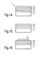
- Figure 14 schematically shows the structure of Figure 13 after a removal step of the auxiliary carrier and the dielectric layer;
- Figure 15 schematically shows the structure of Figure 14 after the removal of a semi-conducting nitride layer; and
- Figure 16 schematically shows a preparation of an electrical contact on the structure of Figure 15.
- It should be noted that the dimensions shown in the Figures are not true to scale.
- While the present invention is described with reference to the embodiments as illustrated in the following detailed description as well as in the drawings, it should be understood that the following detailed description as well as the drawings are not intended to limit the present invention to the particular illustrative embodiments disclosed, but rather to describe the illustrative embodiments merely exemplifying the various aspects of the present invention, the scope of which is defined by the appended claims.
- According to the present invention, an efficient method of producing substrates for optoelectronic applications is provided which may be used to fabricate optoelectronic devices such as LED structures or laser diodes.
- The Figures 1 to 16 show an illustrative process flow of an embodiment of the present invention.
- With reference to Figure 1, a step of providing a massive semi-conducting nitride substrate is shown. In the embodiment shown, the massive semi-conducting nitride substrate is a GaN-
substrate 8 having anitrogen face 18 on top and on its bottom agallium face 19. The massive GaN-substrate has a hexagonal crystal structure with a dislocation density of lower than 106/cm2. The planarity of thesubstrate 8 is in the range of 20 µm. Thenitride substrate 8 has a thickness of about 150 to 750 µm. Thenitrogen face 18 of thenitride substrate 8 is polished and has a surface roughness of lower than 0.3 nm RMS measured with an atomic force microscope (AFM) over a field of some 1x1 µm2. - The above described technology can also be realised using a semi-conducting nitride substrate of GaN with a cubic crystal structure or with a cubic or hexagonal monocrystalline AIN substrate instead of the hexagonal GaN-
substrate 8. In all of these cases, the dislocation density of thesubstrate 8 should be between 105 to 106/cm2 or even lower. - Figure 2 schematically shows a deposition step of a
dielectric layer 9 on the massivesemi-conducting nitride substrate 8. This deposition step is performed on thenitrogen face 18 of thenitride substrate 8. Thedielectric layer 9 can be a material selected from a group comprising silicon dioxide, silicon nitride, a combination of these materials or other dielectric materials which have a good adhesion to thenitrogen face 18 of the GaN-substrate 8. The dielectric layer(s) 9 are favourably deposited by chemical vapour deposition. Although not absolutely necessary, the structure shown in Figure 2 can be thermally annealed to densify the dielectric layer(s) 9. - As illustrated in Figure 3, the structure shown in Figure 2 is implanted with
species 10 in an implantation step. Thespecies 10 can be of hydrogen, helium or other elements alone or in combination. In the embodiment shown, thespecies 10 are implanted with energies between 20 and 200 keV and with doses between 1015 and 1018 at/cm2. Thespecies 10 are implanted in a certain depth d of thenitride substrate 8 forming there apredetermined splitting area 11, at and around the implantation depth d. - According to Figure 4, the implanted structure of Figure 3 is bonded on its implanted side with an
auxiliary carrier 6. Theauxiliary carrier 6 is preferably a silicon substrate, GaAs substrate or a ZnO substrate but can also be of another material which has relatively high mechanical stability since this material will be highly stressed during a following Smart Cut™ process in which thenitride substrate 8 is split. In the case of GaAs or ZnO asauxiliary substrate 6, the thermal dilatation coefficient of theauxiliary carrier 6 is chosen or adapted in such a way that it is slowly higher than the thermal dilatation coefficient of GaN, resulting in a structure having a GaN-layer with a slight compression preventing an appearance of cracking in this layer. - As shown in Figure 5, the structure of Figure 4 is split into two parts with thermal and/or mechanical treatment. The stress applied due to that treatment leads to the splitting of the structure of Figure 4 along the
predetermined splitting area 11. The splitting step results in two structures, a residual part of the formersemi-conductive nitride substrate 8 and an auxiliary substrate 5 consisting of theauxiliary carrier 6, thedielectric layer 9 and asemi-conducting nitride layer 2 being a part of the formersemi-conducting nitride substrate 8. The split structures have splitsurfaces 14 and 22 with an increased roughness after the splitting step. - With reference to Figure 6, the auxiliary substrate 5 is smoothed in a polishing step applied on the
split surface 14 of thenitride layer 2. After this polishing step, the surface roughness of the GaN-layer 2 is of an atomic level which is only several Angstroms when measured with an AFM. - In the next step, shown in Figure 7, a
protective layer 13 is deposited on thesurface 14 of the GaN-layer 2. Theprotective layer 13 is preferably a dielectric layer. - As shown in Figure 8, the structure of Figure 7 is thermally annealed in an
annealing equipment 20. The structure is thermally treated in a temperature region between 500 and 1100 °C in a gaseous atmosphere which permits preservation of the crystal quality of the GaN-layer 2. The annealing step shown in Figure 8 can also be applied before the polishing step shown in Figure 6 and can also be applied directly onto the auxiliary substrate 5 without the deposition of theprotective layer 13 before the annealing step. The thermal annealing step leads to an enforcement of the bonding forces at the interface between theauxiliary carrier 6 and thedielectric layer 9. - As shown in Figure 9, the
protective layer 13 which can be deposited before the annealing step shown in Figure 8, is removed in a removal step. In a favourable example of the invention, theprotective layer 13 can be removed with a chemical treatment, for instance with HF. The removal step results in the auxiliary substrate 5 having a smooth andclean gallium face 14 on top of the GaN-layer 2. The GaN-layer 2 is monocrystalline with a crystal quality equivalent to the crystal quality of the massivesemi-conducting nitride substrate 8 as shown in Figure 1. The surface of the GaN-layer 2 is nearly free from particles. The thickness of the GaN-layer 2 is, in one favourable example of the invention, about 200nm. - With reference to Figure 10, in a further step an
epitaxial layer 15 is deposited on thegallium face 14 of the GaN-layer 2. Theepitaxial layer 15 can be deposited with a known epitaxy method like MOCVD, MBE or HVPE. The temperature applied during the epitaxial deposition step is in the range between 700 and 1100°C. - For example, the epitaxial layer(s) deposited in the step shown in Figure 10 can be: of n-type GaN doped with Si and having a thickness of about 0.2 µm, of InGaN, of AlGaN and/or of p-type GaN doped with Mg. The total thickness of the epitaxial layer(s) 15 is, in a favourable example of the invention, about 0.5 µm. The composition of the epitaxial layer(s) depends on the efficiency and the wavelength of the optoelectronic structure which shall be fabricated with the resulting substrate. The dislocation density of the epitaxial layer(s) 15 is nearly equivalent to the dislocation density of the original GaN-
substrate 8, that means lower than 106/cm2. It is generally advantageous to have epitaxial layer(s) with an increased thickness to advance current propagation in the active layer(s) of the resulting structure. - In a next step, shown in Figure 11, a metal layer 4 is deposited on the epitaxial layer(s) 15. The metal layer 4 serves later as an Ohmic contact to contact the resulting structure electrically. The metal layer 4 can be of Ni/Au, Pt, rhodium or another conductive material.
- With reference to Figure 12, a
final carrier 7 is provided on which areflection layer 17 is deposited. Thefinal carrier 7 serves as a support substrate which is electrically conductive with a low electrical resistivity and a good thermal conductivity. Thefinal carrier 7 can be of silicon, SiC, copper or another conductive or semi-conducting material. Thereflection layer 17 can be for instance of gold, aluminium or silver which materials have good reflectivity. Thereflection layer 17 acts later as a mirror layer arranged between thefinal carrier 7 and the epitaxial layer(s) 15. Said mirror is chosen depending on the emitted wavelength(s) of the resulting structure. - As illustrated in Figure 13, the structures of Figures 11 and 12 are connected on the metal layer 4 and the
reflection layer 17 in a bonding step. The bonding step leads to a molecular adhesion between the structures of Figures 11 and 12 to provide a contact therebetween using mechanical pressure and a certain temperature. - As shown in Figure 14, in a further step the
auxiliary carrier 6 and thedielectric layer 9 are removed from the bonded structure in a removal step. The removal step can comprise mechanical lapping and/or polishing as well as a chemical attack using thegallium nitride layer 2 as an etch stop layer. If thefinal carrier 7 is of silicon, the removal can be realised using mechanical treatment followed by chemical treatment based on a TMAH or HF/HNO3 solution. Said chemical attack can be realised by immersing the structure in a bath of said solution using an equipment with which the structure can be held in rotation and in which the auxiliary carrier can be exposed to the chemical solution. The removal of the auxiliary carrier can also be realised by using only chemical treatment. - In a next step shown in Figure 15, the
gallium nitride layer 2 is removed from the structure shown in Figure 14. A removal of inutile layers, such as the non-doped GaN-layer 2 can result in an enhancement of efficiency of the resulting structure since such layers would only lead to an unfortunate absorption of photons. GaN absorbs, for instance, UV radiation. - With reference to Figure 16, an
electrical contact 21 is provided on the epitaxial layer(s) 15. - The resulting structure consists of the
final carrier 7, thereflection layer 17, the metal layer 4, the epitaxial layer(s) 15 and theelectrical contact 21. The metal layer 4 and thereflection layer 17 form together a metallic junction or metallic intermediate layer between thecarrier substrate 7 and the epitaxial layer(s) 15. The metallic intermediate layer can include or not include thereflection layer 17. - In following steps which are not shown, the structure shown in Figure 16 is further processed by using lithographic and etch steps for chip fabrication, deposition steps of dielectric layers for preservation of the structure and deposition steps of metal layers to realise contacts on both sides of the structure. As last steps, the fabricated structures are separated into chips which are packaged finally.
- With the inventive method, a substrate with an active layer of very good crystal quality and with eliminated inutile layers can be realised for optoelectronic applications. The good crystal quality is very important for a high efficiency and long life span of the structures, in particular for LED structures of laser diodes. Furthermore, due to the elimination of GaN inutile layers in the inventive method allows minimisation of photon absorption in the active layer(s) resulting in a high efficiency of light radiation.
The inventive technology uses the very good crystallinity of the massive nitride substrate in a direct transfer of a part of said substrate to the final substrate. This way, the final active epitaxial layer(s) can be grown directly on the high quality transferred part with the same good crystallinity leading to high quality final structures.
Claims (15)
- A method of producing a substrate (1) for an optoelectronic application, the substrate (1) having at least one active nitride layer (2, 15) on a final carrier (7) and a metallic intermediate layer (4) therebetween, wherein the method comprises: preparing of an auxiliary substrate (5) wherein one semi-conducting nitride layer (2) is placed on an auxiliary carrier (6);
metallising the auxiliary substrate (5) on the side of the nitride layer (2);
bonding of the metallised auxiliary substrate (5) with the final carrier (7); and
removing of the auxiliary carrier (6) after the bonding step
characterised in that
the step of preparing the auxiliary substrate (5) comprises:detaching of a part from a massive semi-conducting nitride substrate (8); andtransferring said part onto the auxiliary carrier (6) to form thereon the semi-conducting nitride layer (2). - The method of claim 1, characterised in that the semi-conducting nitride substrate (8) is a GaN-substrate or an AlN substrate.
- The method of one of the claims 1 or 2, characterised in that the massive semi-conducting nitride substrate (8) is produced with a dislocation density of less than 10^6/cm2.
- The method of one of the preceding claims, characterised in that the step of detaching and transferring comprises:depositing of a dielectric layer (9) on the semi-conducting nitride substrate (8); implanting species (10) through the dielectric layer (9) into a certain depth (d) of the nitride substrate (8) to form therein a predetermined splitting area (11);bonding of the nitride substrate (8) on the implanted side (12) with the auxiliary carrier (6); andthermal and/or mechanical treating of the nitride substrate (8) to split said substrate (8) along the predetermined splitting area (11).
- The method of one of the preceding claims, characterised in that the auxiliary carrier (6) is a substrate selected from a group of materials comprising silicon, GaAs and ZnO.
- The method of one of the preceding claims, characterised in that the auxiliary substrate (5) is annealed after the detaching and transferring step.
- The method of claim 6, characterised in that a protective layer (13) is deposited onto the transferred nitride layer (2) before the annealing step and is removed after the annealing step.
- The method of one of the preceding claims, characterised in that the surface (14) of the transferred nitride layer (2) is smoothed after the detaching and transferring step or after the annealing step.
- The method of one of the preceding claims, characterised in that at least one epitaxial nitride layer (15) of a material of a group comprising n-type GaN, InGaN, AlGaN, undoped GaN and p-type GaN is deposited on the transferred nitride layer (2) of the auxiliary substrate (5).
- The method of claim 9, characterised in that the metallic intermediate layer (4) is deposited on the at least one epitaxial nitride layer (15).
- The method of claim 10, characterised in that the method further comprises providing the final carrier (7) and bonding of said final carrier (7) on the metallised side (16) of the auxiliary substrate (5).
- The method of claim 11, characterised in that the material of the final carrier (7) is selected from a group comprising silicon, silicon carbide and copper.
- The method of one of the claims 11 or 12, characterised in that at least one reflection layer (17) is deposited onto the final carrier (7) before the bonding step of the final carrier (7) with the auxiliary substrate (5).
- The method of one of the claims 11 to 13, characterised in that the auxiliary carrier (6) is mechanically and/or chemically removed after the bonding step, wherein the nitride layer (2) is used as a stop layer for the removal step.
- The method of claim 14, characterised therein that the transferred nitride layer (2) is removed from the substrate (1) after the removal step of the auxiliary carrier (6).
Priority Applications (8)
| Application Number | Priority Date | Filing Date | Title |
|---|---|---|---|
| EP05290082A EP1681712A1 (en) | 2005-01-13 | 2005-01-13 | Method of producing substrates for optoelectronic applications |
| US11/084,747 US7537949B2 (en) | 2005-01-13 | 2005-03-21 | Optoelectronic substrate and methods of making same |
| CN200680001546A CN100580880C (en) | 2005-01-13 | 2006-01-12 | Method for producing a substrate for optoelectronic applications |
| PCT/EP2006/000230 WO2006074933A1 (en) | 2005-01-13 | 2006-01-12 | Method of producing a substrate for an optoelectronic application |
| JP2007550755A JP5312797B2 (en) | 2005-01-13 | 2006-01-12 | Method for producing optoelectronic substrate |
| KR1020077014329A KR100905977B1 (en) | 2005-01-13 | 2006-01-12 | Method of Producing a Substrate for an Optoelectronic Application |
| US12/424,868 US20090200569A1 (en) | 2005-01-13 | 2009-04-16 | Optoelectronic substrate and methods of making same |
| US13/154,510 US8541290B2 (en) | 2005-01-13 | 2011-06-07 | Optoelectronic substrate and methods of making same |
Applications Claiming Priority (1)
| Application Number | Priority Date | Filing Date | Title |
|---|---|---|---|
| EP05290082A EP1681712A1 (en) | 2005-01-13 | 2005-01-13 | Method of producing substrates for optoelectronic applications |
Publications (1)
| Publication Number | Publication Date |
|---|---|
| EP1681712A1 true EP1681712A1 (en) | 2006-07-19 |
Family
ID=34941890
Family Applications (1)
| Application Number | Title | Priority Date | Filing Date |
|---|---|---|---|
| EP05290082A Ceased EP1681712A1 (en) | 2005-01-13 | 2005-01-13 | Method of producing substrates for optoelectronic applications |
Country Status (6)
| Country | Link |
|---|---|
| US (3) | US7537949B2 (en) |
| EP (1) | EP1681712A1 (en) |
| JP (1) | JP5312797B2 (en) |
| KR (1) | KR100905977B1 (en) |
| CN (1) | CN100580880C (en) |
| WO (1) | WO2006074933A1 (en) |
Cited By (2)
| Publication number | Priority date | Publication date | Assignee | Title |
|---|---|---|---|---|
| FR2914494A1 (en) * | 2007-03-28 | 2008-10-03 | Soitec Silicon On Insulator | METHOD FOR DEFERING A THIN LAYER OF MATERIAL |
| EP2105972A3 (en) * | 2008-03-28 | 2015-06-10 | Semiconductor Energy Laboratory Co, Ltd. | Photoelectric conversion device and method for manufacturing the same |
Families Citing this family (44)
| Publication number | Priority date | Publication date | Assignee | Title |
|---|---|---|---|---|
| US10374120B2 (en) * | 2005-02-18 | 2019-08-06 | Koninklijke Philips N.V. | High efficiency solar cells utilizing wafer bonding and layer transfer to integrate non-lattice matched materials |
| TW200707799A (en) * | 2005-04-21 | 2007-02-16 | Aonex Technologies Inc | Bonded intermediate substrate and method of making same |
| TWI267946B (en) * | 2005-08-22 | 2006-12-01 | Univ Nat Chiao Tung | Interconnection of group III-V semiconductor device and fabrication method for making the same |
| CN100474642C (en) * | 2005-10-27 | 2009-04-01 | 晶能光电(江西)有限公司 | Indium gallium aluminium nitrogen semi-conductor luminous element containing metallic chromium substrate and manufacturing method thereof |
| US20070243703A1 (en) * | 2006-04-14 | 2007-10-18 | Aonex Technololgies, Inc. | Processes and structures for epitaxial growth on laminate substrates |
| US7732301B1 (en) | 2007-04-20 | 2010-06-08 | Pinnington Thomas Henry | Bonded intermediate substrate and method of making same |
| US20080303033A1 (en) * | 2007-06-05 | 2008-12-11 | Cree, Inc. | Formation of nitride-based optoelectronic and electronic device structures on lattice-matched substrates |
| WO2009015337A1 (en) * | 2007-07-26 | 2009-01-29 | S.O.I.Tec Silicon On Insulator Technologies | Methods for producing improved epitaxial materials |
| KR101374090B1 (en) * | 2007-07-26 | 2014-03-17 | 아리조나 보드 오브 리젠츠 퍼 앤 온 비하프 오브 아리조나 스테이트 유니버시티 | Epitaxial methods and templates grown by the methods |
| US20090278233A1 (en) * | 2007-07-26 | 2009-11-12 | Pinnington Thomas Henry | Bonded intermediate substrate and method of making same |
| US7781780B2 (en) | 2008-03-31 | 2010-08-24 | Bridgelux, Inc. | Light emitting diodes with smooth surface for reflective electrode |
| US20100295088A1 (en) * | 2008-10-02 | 2010-11-25 | Soraa, Inc. | Textured-surface light emitting diode and method of manufacture |
| FR2936903B1 (en) * | 2008-10-07 | 2011-01-14 | Soitec Silicon On Insulator | RELAXING A LAYER OF CONTAMINATED MATERIAL WITH APPLICATION OF A STIFFENER |
| KR101408475B1 (en) | 2008-10-30 | 2014-06-19 | 소이텍 | Methods of forming layers of semiconductor material having reduced lattice strain, semiconductor structures, devices and engineered substrates including same |
| US8637383B2 (en) | 2010-12-23 | 2014-01-28 | Soitec | Strain relaxation using metal materials and related structures |
| US8247886B1 (en) | 2009-03-09 | 2012-08-21 | Soraa, Inc. | Polarization direction of optical devices using selected spatial configurations |
| US8791499B1 (en) | 2009-05-27 | 2014-07-29 | Soraa, Inc. | GaN containing optical devices and method with ESD stability |
| US8409366B2 (en) * | 2009-06-23 | 2013-04-02 | Oki Data Corporation | Separation method of nitride semiconductor layer, semiconductor device, manufacturing method thereof, semiconductor wafer, and manufacturing method thereof |
| US9000466B1 (en) | 2010-08-23 | 2015-04-07 | Soraa, Inc. | Methods and devices for light extraction from a group III-nitride volumetric LED using surface and sidewall roughening |
| US9293644B2 (en) | 2009-09-18 | 2016-03-22 | Soraa, Inc. | Power light emitting diode and method with uniform current density operation |
| DE112010003700T5 (en) | 2009-09-18 | 2013-02-28 | Soraa, Inc. | POWER LIGHT DIODE AND METHOD WITH POWER DENSITY OPERATION |
| US9583678B2 (en) | 2009-09-18 | 2017-02-28 | Soraa, Inc. | High-performance LED fabrication |
| US8933644B2 (en) | 2009-09-18 | 2015-01-13 | Soraa, Inc. | LED lamps with improved quality of light |
| US8648387B2 (en) * | 2009-12-30 | 2014-02-11 | Industrial Technology Research Institute | Nitride semiconductor template and method of manufacturing the same |
| US8905588B2 (en) | 2010-02-03 | 2014-12-09 | Sorra, Inc. | System and method for providing color light sources in proximity to predetermined wavelength conversion structures |
| US8740413B1 (en) | 2010-02-03 | 2014-06-03 | Soraa, Inc. | System and method for providing color light sources in proximity to predetermined wavelength conversion structures |
| US10147850B1 (en) | 2010-02-03 | 2018-12-04 | Soraa, Inc. | System and method for providing color light sources in proximity to predetermined wavelength conversion structures |
| US9450143B2 (en) | 2010-06-18 | 2016-09-20 | Soraa, Inc. | Gallium and nitrogen containing triangular or diamond-shaped configuration for optical devices |
| US8786053B2 (en) | 2011-01-24 | 2014-07-22 | Soraa, Inc. | Gallium-nitride-on-handle substrate materials and devices and method of manufacture |
| FR2977069B1 (en) | 2011-06-23 | 2014-02-07 | Soitec Silicon On Insulator | METHOD FOR MANUFACTURING A SEMICONDUCTOR STRUCTURE USING TEMPORARY COLLAGE |
| US8686431B2 (en) | 2011-08-22 | 2014-04-01 | Soraa, Inc. | Gallium and nitrogen containing trilateral configuration for optical devices |
| KR101254716B1 (en) * | 2011-11-07 | 2013-04-15 | 삼성코닝정밀소재 주식회사 | Manufacturing method of layer transferred substrate having pattern |
| US8912025B2 (en) | 2011-11-23 | 2014-12-16 | Soraa, Inc. | Method for manufacture of bright GaN LEDs using a selective removal process |
| JP5879964B2 (en) * | 2011-11-25 | 2016-03-08 | 住友電気工業株式会社 | Composite substrate manufacturing method and semiconductor device manufacturing method |
| US9269876B2 (en) | 2012-03-06 | 2016-02-23 | Soraa, Inc. | Light emitting diodes with low refractive index material layers to reduce light guiding effects |
| JP2013247362A (en) * | 2012-05-29 | 2013-12-09 | Samsung Corning Precision Materials Co Ltd | Method for manufacturing thin film bonded substrate for semiconductor element |
| US8971368B1 (en) | 2012-08-16 | 2015-03-03 | Soraa Laser Diode, Inc. | Laser devices having a gallium and nitrogen containing semipolar surface orientation |
| US9978904B2 (en) | 2012-10-16 | 2018-05-22 | Soraa, Inc. | Indium gallium nitride light emitting devices |
| US8802471B1 (en) | 2012-12-21 | 2014-08-12 | Soraa, Inc. | Contacts for an n-type gallium and nitrogen substrate for optical devices |
| US11721547B2 (en) * | 2013-03-14 | 2023-08-08 | Infineon Technologies Ag | Method for manufacturing a silicon carbide substrate for an electrical silicon carbide device, a silicon carbide substrate and an electrical silicon carbide device |
| US8994033B2 (en) | 2013-07-09 | 2015-03-31 | Soraa, Inc. | Contacts for an n-type gallium and nitrogen substrate for optical devices |
| US9548247B2 (en) * | 2013-07-22 | 2017-01-17 | Infineon Technologies Austria Ag | Methods for producing semiconductor devices |
| US9419189B1 (en) | 2013-11-04 | 2016-08-16 | Soraa, Inc. | Small LED source with high brightness and high efficiency |
| JP6803232B2 (en) * | 2014-11-11 | 2020-12-23 | 出光興産株式会社 | New laminate |
Citations (4)
| Publication number | Priority date | Publication date | Assignee | Title |
|---|---|---|---|---|
| US20010042866A1 (en) * | 1999-02-05 | 2001-11-22 | Carrie Carter Coman | Inxalygazn optical emitters fabricated via substrate removal |
| US20030232487A1 (en) * | 2002-06-11 | 2003-12-18 | Fabrice Letertre | Fabrication of substrates with a useful layer of monocrystalline semiconductor material |
| US20040014299A1 (en) * | 2000-11-06 | 2004-01-22 | Hubert Moriceau | Method for making a stacked structure comprising a thin film adhering to a target substrate |
| US20040029359A1 (en) * | 2000-11-27 | 2004-02-12 | Fabrice Letertre | Methods for fabricating a substrate |
Family Cites Families (18)
| Publication number | Priority date | Publication date | Assignee | Title |
|---|---|---|---|---|
| JP2540791B2 (en) * | 1991-11-08 | 1996-10-09 | 日亜化学工業株式会社 | A method for manufacturing a p-type gallium nitride-based compound semiconductor. |
| JP3325713B2 (en) * | 1994-08-22 | 2002-09-17 | ローム株式会社 | Manufacturing method of semiconductor light emitting device |
| JP4024994B2 (en) * | 2000-06-30 | 2007-12-19 | 株式会社東芝 | Semiconductor light emitting device |
| JP2002284600A (en) | 2001-03-26 | 2002-10-03 | Hitachi Cable Ltd | Gallium nitride crystal substrate manufacturing method and gallium nitride crystal substrate |
| JP3886341B2 (en) * | 2001-05-21 | 2007-02-28 | 日本電気株式会社 | Method for manufacturing gallium nitride crystal substrate and gallium nitride crystal substrate |
| US6936357B2 (en) * | 2001-07-06 | 2005-08-30 | Technologies And Devices International, Inc. | Bulk GaN and ALGaN single crystals |
| CN100403543C (en) * | 2001-12-04 | 2008-07-16 | 信越半导体株式会社 | Bonded wafer and method for manufacturing bonded wafer |
| FR2834123B1 (en) * | 2001-12-21 | 2005-02-04 | Soitec Silicon On Insulator | SEMICONDUCTOR THIN FILM DELIVERY METHOD AND METHOD FOR OBTAINING A DONOR WAFER FOR SUCH A DELAYING METHOD |
| FR2835095B1 (en) | 2002-01-22 | 2005-03-18 | PROCESS FOR PREPARING SEPARABLE SEMICONDUCTOR ASSEMBLIES, IN PARTICULAR FOR FORMING SUBSTRATES FOR ELECTRONICS, OPTOELECTRIC, AND OPTICS | |
| TW577178B (en) | 2002-03-04 | 2004-02-21 | United Epitaxy Co Ltd | High efficient reflective metal layer of light emitting diode |
| US6791120B2 (en) | 2002-03-26 | 2004-09-14 | Sanyo Electric Co., Ltd. | Nitride-based semiconductor device and method of fabricating the same |
| US20030189215A1 (en) * | 2002-04-09 | 2003-10-09 | Jong-Lam Lee | Method of fabricating vertical structure leds |
| JP5142523B2 (en) * | 2003-06-04 | 2013-02-13 | チェオル ユー,ミュング | Vertical structure composite semiconductor device |
| TWI240434B (en) | 2003-06-24 | 2005-09-21 | Osram Opto Semiconductors Gmbh | Method to produce semiconductor-chips |
| JP4232605B2 (en) * | 2003-10-30 | 2009-03-04 | 住友電気工業株式会社 | Nitride semiconductor substrate manufacturing method and nitride semiconductor substrate |
| US7118813B2 (en) * | 2003-11-14 | 2006-10-10 | Cree, Inc. | Vicinal gallium nitride substrate for high quality homoepitaxy |
| US7148124B1 (en) * | 2004-11-18 | 2006-12-12 | Alexander Yuri Usenko | Method for forming a fragile layer inside of a single crystalline substrate preferably for making silicon-on-insulator wafers |
| US20060124956A1 (en) * | 2004-12-13 | 2006-06-15 | Hui Peng | Quasi group III-nitride substrates and methods of mass production of the same |
-
2005
- 2005-01-13 EP EP05290082A patent/EP1681712A1/en not_active Ceased
- 2005-03-21 US US11/084,747 patent/US7537949B2/en not_active Expired - Lifetime
-
2006
- 2006-01-12 KR KR1020077014329A patent/KR100905977B1/en not_active Expired - Lifetime
- 2006-01-12 CN CN200680001546A patent/CN100580880C/en not_active Expired - Lifetime
- 2006-01-12 JP JP2007550755A patent/JP5312797B2/en not_active Expired - Lifetime
- 2006-01-12 WO PCT/EP2006/000230 patent/WO2006074933A1/en not_active Ceased
-
2009
- 2009-04-16 US US12/424,868 patent/US20090200569A1/en not_active Abandoned
-
2011
- 2011-06-07 US US13/154,510 patent/US8541290B2/en not_active Expired - Fee Related
Patent Citations (4)
| Publication number | Priority date | Publication date | Assignee | Title |
|---|---|---|---|---|
| US20010042866A1 (en) * | 1999-02-05 | 2001-11-22 | Carrie Carter Coman | Inxalygazn optical emitters fabricated via substrate removal |
| US20040014299A1 (en) * | 2000-11-06 | 2004-01-22 | Hubert Moriceau | Method for making a stacked structure comprising a thin film adhering to a target substrate |
| US20040029359A1 (en) * | 2000-11-27 | 2004-02-12 | Fabrice Letertre | Methods for fabricating a substrate |
| US20030232487A1 (en) * | 2002-06-11 | 2003-12-18 | Fabrice Letertre | Fabrication of substrates with a useful layer of monocrystalline semiconductor material |
Non-Patent Citations (2)
| Title |
|---|
| LUO Z S ET AL: "ENHANCEMENT OF (IN,GAN)N LIGHT-EMITTING DIODE PERFORMANCE BY LASE LIFTOFF AND TRANSFER FROM SAPPHIRE TO SILICON", IEEE PHOTONICS TECHNOLOGY LETTERS, IEEE INC. NEW YORK, US, vol. 14, no. 10, October 2002 (2002-10-01), pages 1400 - 1402, XP001175396, ISSN: 1041-1135 * |
| NORTHRUP J ET AL: "Strong affinity of hydrogen for the GaN(000-1) surface: Implications for molecular beam epitaxy and metalorganic chemical vapor deposition", 1 January 2004, APPLIED PHYSICS LETTERS, A I P PUBLISHING LLC, US, PAGE(S) 3429 - 3431, ISSN: 0003-6951, XP012062977 * |
Cited By (2)
| Publication number | Priority date | Publication date | Assignee | Title |
|---|---|---|---|---|
| FR2914494A1 (en) * | 2007-03-28 | 2008-10-03 | Soitec Silicon On Insulator | METHOD FOR DEFERING A THIN LAYER OF MATERIAL |
| EP2105972A3 (en) * | 2008-03-28 | 2015-06-10 | Semiconductor Energy Laboratory Co, Ltd. | Photoelectric conversion device and method for manufacturing the same |
Also Published As
| Publication number | Publication date |
|---|---|
| JP5312797B2 (en) | 2013-10-09 |
| CN100580880C (en) | 2010-01-13 |
| US7537949B2 (en) | 2009-05-26 |
| US20090200569A1 (en) | 2009-08-13 |
| KR100905977B1 (en) | 2009-07-06 |
| US20110237008A1 (en) | 2011-09-29 |
| JP2008527731A (en) | 2008-07-24 |
| US8541290B2 (en) | 2013-09-24 |
| CN101091234A (en) | 2007-12-19 |
| US20060166390A1 (en) | 2006-07-27 |
| WO2006074933A1 (en) | 2006-07-20 |
| KR20070089821A (en) | 2007-09-03 |
Similar Documents
| Publication | Publication Date | Title |
|---|---|---|
| US7537949B2 (en) | Optoelectronic substrate and methods of making same | |
| US8101498B2 (en) | Bonded intermediate substrate and method of making same | |
| JP4677065B2 (en) | Light emitting diode and manufacturing method thereof | |
| US7732301B1 (en) | Bonded intermediate substrate and method of making same | |
| US5502316A (en) | Wafer bonding of light emitting diode layers | |
| KR100773997B1 (en) | Gallium nitride-based devices and manufacturing process | |
| US6611004B2 (en) | Gallium nitride based light emitting element | |
| TWI240434B (en) | Method to produce semiconductor-chips | |
| US8884306B2 (en) | Semiconductor device and method for manufacturing the same | |
| US20090278233A1 (en) | Bonded intermediate substrate and method of making same | |
| TWI532209B (en) | Method for forming a buried metal layer structure | |
| US8502264B2 (en) | Composite substrate, and method for the production of a composite substrate | |
| TWI407491B (en) | Method of separating semiconductor and its substrate | |
| US9647174B2 (en) | Optoelectronic semiconductor chip | |
| JP2006521984A (en) | Method for fabricating a group III nitride device and the device so fabricated | |
| TWI803485B (en) | Vertical gallium nitride schottky diode methods | |
| JPH10321911A (en) | Method for producing compound semiconductor epitaxy layer on single crystal silicon and light emitting diode produced thereby | |
| CN104576861A (en) | Semiconductor buffer structure, semiconductor device, and method of manufacturing the semiconductor device | |
| US20060124956A1 (en) | Quasi group III-nitride substrates and methods of mass production of the same | |
| KR20090018451A (en) | Method for manufacturing vertical gallium-based LED device | |
| KR101428066B1 (en) | vertical structured group 3 nitride-based light emitting diode and its fabrication methods | |
| KR101480551B1 (en) | vertical structured group 3 nitride-based light emitting diode and its fabrication methods | |
| US7446346B2 (en) | Semiconductor substrate for optoelectronic components and method for fabricating it | |
| US8658446B2 (en) | Method for fabricating semiconductor substrate for optoelectronic components | |
| KR100814920B1 (en) | Vertical structure nitride semiconductor light emitting device and manufacturing method thereof |
Legal Events
| Date | Code | Title | Description |
|---|---|---|---|
| PUAI | Public reference made under article 153(3) epc to a published international application that has entered the european phase |
Free format text: ORIGINAL CODE: 0009012 |
|
| 17P | Request for examination filed |
Effective date: 20060118 |
|
| AK | Designated contracting states |
Kind code of ref document: A1 Designated state(s): AT BE BG CH CY CZ DE DK EE ES FI FR GB GR HU IE IS IT LI LT LU MC NL PL PT RO SE SI SK TR |
|
| AX | Request for extension of the european patent |
Extension state: AL BA HR LV MK YU |
|
| AKX | Designation fees paid |
Designated state(s): AT BE BG CH CY CZ DE DK EE ES FI FR GB GR HU IE IS IT LI LT LU MC NL PL PT RO SE SI SK TR |
|
| RAP1 | Party data changed (applicant data changed or rights of an application transferred) |
Owner name: SOITEC |
|
| STAA | Information on the status of an ep patent application or granted ep patent |
Free format text: STATUS: THE APPLICATION HAS BEEN REFUSED |
|
| 18R | Application refused |
Effective date: 20190409 |