EP1681610A2 - System clock distributing apparatus and system clock distributing method - Google Patents
System clock distributing apparatus and system clock distributing method Download PDFInfo
- Publication number
- EP1681610A2 EP1681610A2 EP05252671A EP05252671A EP1681610A2 EP 1681610 A2 EP1681610 A2 EP 1681610A2 EP 05252671 A EP05252671 A EP 05252671A EP 05252671 A EP05252671 A EP 05252671A EP 1681610 A2 EP1681610 A2 EP 1681610A2
- Authority
- EP
- European Patent Office
- Prior art keywords
- synchronizing signal
- clock
- internal clock
- frequency
- generates
- Prior art date
- Legal status (The legal status is an assumption and is not a legal conclusion. Google has not performed a legal analysis and makes no representation as to the accuracy of the status listed.)
- Withdrawn
Links
Images



Classifications
-
- G—PHYSICS
- G06—COMPUTING OR CALCULATING; COUNTING
- G06F—ELECTRIC DIGITAL DATA PROCESSING
- G06F1/00—Details not covered by groups G06F3/00 - G06F13/00 and G06F21/00
- G06F1/04—Generating or distributing clock signals or signals derived directly therefrom
- G06F1/12—Synchronisation of different clock signals provided by a plurality of clock generators
-
- G—PHYSICS
- G06—COMPUTING OR CALCULATING; COUNTING
- G06F—ELECTRIC DIGITAL DATA PROCESSING
- G06F1/00—Details not covered by groups G06F3/00 - G06F13/00 and G06F21/00
- G06F1/04—Generating or distributing clock signals or signals derived directly therefrom
-
- G—PHYSICS
- G06—COMPUTING OR CALCULATING; COUNTING
- G06F—ELECTRIC DIGITAL DATA PROCESSING
- G06F1/00—Details not covered by groups G06F3/00 - G06F13/00 and G06F21/00
- G06F1/04—Generating or distributing clock signals or signals derived directly therefrom
- G06F1/06—Clock generators producing several clock signals
-
- G—PHYSICS
- G06—COMPUTING OR CALCULATING; COUNTING
- G06F—ELECTRIC DIGITAL DATA PROCESSING
- G06F1/00—Details not covered by groups G06F3/00 - G06F13/00 and G06F21/00
- G06F1/04—Generating or distributing clock signals or signals derived directly therefrom
- G06F1/10—Distribution of clock signals, e.g. skew
Definitions
- the present invention relates to a system clock distributing apparatus and a system clock distributing method for controlling a clock generation for a data transmission in a multiprocessor system.
- Multiprocessor server systems have been developed is advanced in recent server systems, and there is a trend toward the further larger scale systems.
- a data transmission except an IO system is required to be a high throughput and low latency in order to speed up a computing process.
- FIG. 4 is a block diagram showing an example of a construction of the inter-chip data transmission unit.
- the inter-chip data transmission unit has a transmission side chip 130 and a reception side chip 140.
- the reception side chip 140 has a data writing unit 141, a ring buffer 142, and a data reading unit 143.
- the same system clock and synchronizing signal are supplied from an external unit to the transmission side chip 130 and the reception side chip 140.
- the transmission side chip 130 transmits an inputted system clock as a writing clock to the reception side chip 140, latches the inputted synchronizing signal and the transmitting data with respect to the system clock, and transmits the inputted synchronizing signal and the transmitting data to the reception side chip 140.
- the data writing unit 141 writes the data from the transmission side chip 130 to the ring buffer 142 at the timing of the writing clock.
- the data writing unit 141 resets a writing pointer for designating a writing position according to the synchronizing signal from the transmission side chip 130 latched by the writing clock, and instructs the ring buffer 142.
- the data reading unit 143 reads out the data of the ring buffer 142 at the timing of the system clock.
- the data reading unit 143 resets the reading pointer for designating a reading position according to the synchronizing signal from an external unit latched by the system clock, and instructs the ring buffer 142.
- accurate writing can be performed by sending, from the transmission side chip 130 to the reception side chip 140, the writing clock with the synchronizing signal and the data, and accurate reading can be performed by sending the system clock and the synchronizing signal from the external unit to the transmission side chip 130 and the reception side chip 140.
- FIG. 5 is a block diagram showing an example of a construction of a system clock distributing apparatus in a previously considered multiprocessor system.
- FIG. 5 shows only a connection relating to the clock and the synchronizing signal.
- This system clock distributing apparatus has an oscillator 1, a PLL (Phase Locked Loop) 102, a clock distributor 103, a plurality of system boards 104, a crossbar board 105, and a back plane 6.
- PLL Phase Locked Loop
- the system clock (period T) and the synchronizing signal (period nT) are generated by the PLL 102 on the basis of the signal generated from the oscillator 1, and distributed from the clock distributor 103 to the system board 104 and the crossbar board 105 through the back plane 6.
- FIG. 6 is a block diagram showing an example of a construction of a previously considered system board.
- FIG. 6 shows only a connection relating to the clock and the synchronizing signal.
- the system board 104 has a clock regulator 111, an NB (north bridge) 112, a plurality of CPUs (Central Processing Unit) 113, and a plurality of MACs (Memory Access Controller) 114.
- the clock regulator 111 receives the system clock and the synchronizing signal from the clock distributor 103, regulates a delay time of the system clock by using the synchronizing signal, and distributes the system clock and the synchronizing signal to the NB 112 and the plurality of MACs 114.
- the NB 112 controls communication with the CPUs 113, the MACs 114, and other NBs, and distributes the system clock and the synchronizing signal received from the clock regulator 111 to the CPU 113.
- the CPU 113 accesses to a memory (not shown) connected to each MAC 114, and conducts a computing process.
- the MAC 114 controls an access from the CPU 113 to the memory.
- FIG. 7 is a block diagram showing an example of a construction of a previously considered crossbar board.
- FIG. 7 shows only a connection relating to the clock and the synchronizing signal.
- the crossbar board 105 has a clock regulator 121, and a plurality of XBs (Cross Bar) 122.
- the clock regulator 121 receives the system clock and the synchronizing signal from the clock distributor 103, regulates a delay time of the system clock by using the synchronizing signal, and distributes the system clock and the synchronizing signal to the plurality of XBs 122.
- the XB 122 connects between the NB 112.
- Japanese Patent Application Laid-Open Publication No. 9-233060 (Pages 3-5, FIG. 1) is known.
- This clock supply system operates an LSI in a substrate by using a global clock supplied from an outside source instead of the local clock in the substrate.
- the substrate can be operated even when the global clock is cut off due to an accident, or at the time of a test of a single substrate,.
- the clock regulators 111, 121 are required to operate as fast as other chips and are a special purpose chip, manufacturing cost of the apparatus becomes very high. Further, since it is necessary to externally adjust the delay time for each route, man-hour becomes very large. Therefore, even if the skew is suppressed to certain degree, its cost demerit is large. Furthermore, even if the adjustment is executed, it might not fall always within an adjustable range, resulting in a lowering of the go-through rate.
- a system clock distributing apparatus for matching a timing of data by using a synchronizing signal, comprises: a synchronizing signal generator that generates a periodical synchronizing signal; a memory that stores the data; at least one processor that conducts a computing process using the data stored in the memory; at least one memory access controller that controls an access from the processor to the memory; and at least one controller that generates an internal clock having a frequency that is an integral multiple of the synchronizing signal based on the synchronizing signal and controls the processor and the memory access controller based on an operation by the internal clock.
- the controller further outputs the synchronizing signal to the processor, and the processor generates an internal clock having a frequency that is an integral multiple of the synchronizing signal based on the synchronizing signal from the controller, and performs the operation by the internal clock.
- the memory access controller generates an internal clock having a frequency that is an integral multiple of the synchronizing signal based on the synchronizing signal, and performs the operation by the internal clock.
- An embodiment of the system clock distributing apparatus further includes at least one crossbar that generates an internal clock having a frequency that is an integral multiple of the synchronizing signal based on the synchronizing signal, and controls a communication among a plurality of the controllers based on an operation by the internal clock.
- a multiprocessor system controller comprises an internal clock generator that generates an internal clock having a frequency that is an integral multiple of an external clock based on the external clock, and a multiprocessor system controller that controls an external processor and an external memory access controller based on an operation by the internal clock.
- a processor comprises an internal clock generator that generates an internal clock having a frequency that is an integral multiple of an external clock based on the external clock; and a processor that conducts a computing process using data stored in an external memory based on an operation by the internal clock.
- a memory access controller comprises an internal clock generator that generates an internal clock having a frequency that is an integral multiple of an external clock based on the external clock; and a memory access processor that controls an access to an external memory based on an operation by the internal clock.
- a crossbar comprises: an internal clock generator that generates an internal clock having a frequency that is an integral multiple of an external clock based on the external clock; and a crossbar processor that controls a communication among a plurality of multiprocessor system controllers based on an operation by the internal clock.
- control step is adapted to output the synchronizing signal to the processing step
- processing step is adapted to generate an internal clock having a frequency that is an integral multiple of the synchronizing signal based on the synchronizing signal from the control step, and perform the operation by the internal clock.
- the memory access control step is adapted to generate an internal clock having a frequency that is an integral multiple of the synchronizing signal based on the synchronizing signal, and perform the operation by the internal clock.
- system clock distributing method further comprises: at least one communication control step that generates the internal clock having a frequency that is an integral multiple of the synchronizing signal based on the synchronizing signal, and controls a communication among a plurality of multiprocessor system controllers based on the operation by the internal clock.
- the processing unit can be a CPU in the above embodiments.
- the controller and the multiprocessor system controller can be an NB in the above embodiments.
- the internal clock generator can be a PLL in the above embodiments.
- the external clock can be a synchronizing signal in the above embodiments.
- the internal clock can be a system clock in the above embodiments.
- the present invention since it is not necessary to use the clock distributor and the clock regulator that operate at high speed and are a special purpose chip, cost reduction can be achieved. A process of externally setting an amount of delay for each route can be omitted, and a lowering of the go-through rate due to not falling within the adjustable range can be prevented. Further, according to the invention, only the synchronizing signal is distributed, thus the number of signals can be reduced. In addition, since the high speed system clock is not distributed, a bottle neck of a transmission speed due to the transmission characteristics of the high speed system clock can be eradicated.
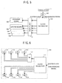
- FIG. 1 is a block diagram showing an example of a construction of a system clock distributing apparatus in a multiprocessor system according to an embodiment of the present invention.
- the same reference numerals as those in FIG. 5 designate the same as or equivalent to those shown in FIG. 5, and the description will be omitted.
- the system clock distributing apparatus of FIG. 1 has, as compared with FIG.
- a synchronizing signal (period nT) is generated by the PLL 2 based on a signal generated from an oscillator 1, and distributed from the clock distributor 3 to the system board 4 and the crossbar board 5 through a back plane 6.
- FIG. 2 is a block diagram showing an example of a construction of a system board according to an embodiment of the present invention.
- the system board 4 has, as compared with FIG. 6, a clock distributor 11 instead of a clock regulator 111, an NB 12 instead of an NB 112, CPUs 13 instead of a CPUs 113, and MACs 14 instead of MACs 114.
- the clock distributor 11 distributes the synchronizing signal inputted from the clock distributor 3 to the plurality of MACs 14.
- the NB 12 is different, as compared with the NB 112, at a point of distributing the synchronizing signal inputted from the clock distributor 3 to the plurality of CPUs 13.
- FIG. 3 is a block diagram showing an example of a construction of the crossbar board according to an embodiment of the present invention.
- the crossbar board 5 has, as compared with FIG. 7, a clock distributor 21 instead of a clock regulator 121, and XBs 22 instead of XBs 122.
- the clock distributor 21 distributes the synchronizing signal inputted from the clock distributor 3 to the plurality of XBs 22.
- the NB 12, the CPU 13, the MAC 14 and the XB 22 each have a PLL for dividing the inputted signal by n times, generate a system clock of period T from the inputted synchronizing signal of period nT, and operate by using the synchronizing signal and the system clock.
- This PLL has characteristics which can assure the phase of the outputted system clock if the phase of the synchronizing signal of the reference clock matched between the chips.
- the system clock distributing apparatus does not distribute the system clock to each chip, but distributes only the synchronizing signal to each chip. Since the skew between the synchronizing signals is not critical, and the synchronizing signals have lower frequency as compared with that of the system clock, problems of the transmission characteristics are little. Therefore, as compared with the conventional system clock distributing apparatus for transmitting the system clock through a long transmission line having large variation between individuals, the system clock distributing apparatus according to embodiments of the present invention can easily match the phase of the system clock with the phase of the synchronizing signal.
Landscapes
- Engineering & Computer Science (AREA)
- Theoretical Computer Science (AREA)
- Physics & Mathematics (AREA)
- General Engineering & Computer Science (AREA)
- General Physics & Mathematics (AREA)
- Multi Processors (AREA)
- Synchronisation In Digital Transmission Systems (AREA)
- Memory System (AREA)
- Manipulation Of Pulses (AREA)
- Stabilization Of Oscillater, Synchronisation, Frequency Synthesizers (AREA)
Abstract
Description
- The present invention relates to a system clock distributing apparatus and a system clock distributing method for controlling a clock generation for a data transmission in a multiprocessor system.
- Multiprocessor server systems have been developed is advanced in recent server systems, and there is a trend toward the further larger scale systems. In such a multiprocessing system, a data transmission except an IO system is required to be a high throughput and low latency in order to speed up a computing process. In view of this demand, it is a key not to use a serial transmission that is generally used in a recent high speed IO, but to transmit a large amount of units of data in a line and to make a transmission side chip and a reception side chip synchronously transmit data in a certain range.
- Here, an inter-chip data transmission unit for performing a data transmission between chips will be described. FIG. 4 is a block diagram showing an example of a construction of the inter-chip data transmission unit. The inter-chip data transmission unit has a
transmission side chip 130 and areception side chip 140. Thereception side chip 140 has adata writing unit 141, aring buffer 142, and adata reading unit 143. The same system clock and synchronizing signal are supplied from an external unit to thetransmission side chip 130 and thereception side chip 140. - The
transmission side chip 130 transmits an inputted system clock as a writing clock to thereception side chip 140, latches the inputted synchronizing signal and the transmitting data with respect to the system clock, and transmits the inputted synchronizing signal and the transmitting data to thereception side chip 140. Thedata writing unit 141 writes the data from thetransmission side chip 130 to thering buffer 142 at the timing of the writing clock. Thedata writing unit 141 resets a writing pointer for designating a writing position according to the synchronizing signal from thetransmission side chip 130 latched by the writing clock, and instructs thering buffer 142. Thedata reading unit 143 reads out the data of thering buffer 142 at the timing of the system clock. Thedata reading unit 143 resets the reading pointer for designating a reading position according to the synchronizing signal from an external unit latched by the system clock, and instructs thering buffer 142. - According to the above-mentioned inter-chip data transmission unit, accurate writing can be performed by sending, from the
transmission side chip 130 to thereception side chip 140, the writing clock with the synchronizing signal and the data, and accurate reading can be performed by sending the system clock and the synchronizing signal from the external unit to thetransmission side chip 130 and thereception side chip 140. - Next, in the case where the above-mentioned inter-chip data transmission unit is applied to a multiprocessor system, a distribution of the system clock and the synchronizing signal to the respective chips on each substrate will specifically be described. FIG. 5 is a block diagram showing an example of a construction of a system clock distributing apparatus in a previously considered multiprocessor system. FIG. 5 shows only a connection relating to the clock and the synchronizing signal. This system clock distributing apparatus has an
oscillator 1, a PLL (Phase Locked Loop) 102, aclock distributor 103, a plurality ofsystem boards 104, acrossbar board 105, and aback plane 6. The system clock (period T) and the synchronizing signal (period nT) are generated by thePLL 102 on the basis of the signal generated from theoscillator 1, and distributed from theclock distributor 103 to thesystem board 104 and thecrossbar board 105 through theback plane 6. - FIG. 6 is a block diagram showing an example of a construction of a previously considered system board. FIG. 6 shows only a connection relating to the clock and the synchronizing signal. The
system board 104 has aclock regulator 111, an NB (north bridge) 112, a plurality of CPUs (Central Processing Unit) 113, and a plurality of MACs (Memory Access Controller) 114. Theclock regulator 111 receives the system clock and the synchronizing signal from theclock distributor 103, regulates a delay time of the system clock by using the synchronizing signal, and distributes the system clock and the synchronizing signal to theNB 112 and the plurality ofMACs 114. The NB 112 controls communication with theCPUs 113, theMACs 114, and other NBs, and distributes the system clock and the synchronizing signal received from theclock regulator 111 to theCPU 113. TheCPU 113 accesses to a memory (not shown) connected to eachMAC 114, and conducts a computing process. TheMAC 114 controls an access from theCPU 113 to the memory. - FIG. 7 is a block diagram showing an example of a construction of a previously considered crossbar board. FIG. 7 shows only a connection relating to the clock and the synchronizing signal. The
crossbar board 105 has aclock regulator 121, and a plurality of XBs (Cross Bar) 122. Theclock regulator 121 receives the system clock and the synchronizing signal from theclock distributor 103, regulates a delay time of the system clock by using the synchronizing signal, and distributes the system clock and the synchronizing signal to the plurality ofXBs 122. The XB 122 connects between the NB 112. - In a system for sending simultaneously the system clock and the synchronizing signal from the
clock distributor 103 as described above, when a skew, that is a deviation of the delay time in the system clock and the synchronizing signal increases, a normal operation cannot be conducted. Therefore, firstly, lengths of wirings are equalized from theclock distributor 103 to each chip. Since unevenness of an element, a substrate, or the like exists, it is difficult to suppress the skew of the clock of high frequency only by the equalization of the lengths. If the frequency of the system clock is low, the reduction in the skew is easy, however the system clock is a central clock of a server, and hence a high frequency is required. Then, to further reduce the skew, theclock regulators - As a conventional art relating to the present invention, for example, Japanese Patent Application Laid-Open Publication No. 9-233060 (Pages 3-5, FIG. 1) is known. This clock supply system operates an LSI in a substrate by using a global clock supplied from an outside source instead of the local clock in the substrate. The substrate can be operated even when the global clock is cut off due to an accident, or at the time of a test of a single substrate,.
- However, since the
clock regulators - It is desirable to overcome the above-mentioned problems, and to provide a system clock distributing apparatus and a system clock distributing method for reducing a skew of a system clock and a synchronizing signal at low cost.
- A system clock distributing apparatus according to one embodiment of an aspect of the present invention for matching a timing of data by using a synchronizing signal, comprises: a synchronizing signal generator that generates a periodical synchronizing signal; a memory that stores the data; at least one processor that conducts a computing process using the data stored in the memory; at least one memory access controller that controls an access from the processor to the memory; and at least one controller that generates an internal clock having a frequency that is an integral multiple of the synchronizing signal based on the synchronizing signal and controls the processor and the memory access controller based on an operation by the internal clock.
- In an embodiment of the system clock distributing apparatus according to this aspect of the invention, the controller further outputs the synchronizing signal to the processor, and the processor generates an internal clock having a frequency that is an integral multiple of the synchronizing signal based on the synchronizing signal from the controller, and performs the operation by the internal clock.
- In an embodiment of the system clock distributing apparatus according to this aspect of the invention, the memory access controller generates an internal clock having a frequency that is an integral multiple of the synchronizing signal based on the synchronizing signal, and performs the operation by the internal clock.
- An embodiment of the system clock distributing apparatus according to this aspect of the present invention further includes at least one crossbar that generates an internal clock having a frequency that is an integral multiple of the synchronizing signal based on the synchronizing signal, and controls a communication among a plurality of the controllers based on an operation by the internal clock.
- A multiprocessor system controller according to one embodiment of another aspect of the present invention comprises an internal clock generator that generates an internal clock having a frequency that is an integral multiple of an external clock based on the external clock, and a multiprocessor system controller that controls an external processor and an external memory access controller based on an operation by the internal clock.
- A processor according to one embodiment of another aspect of the present invention comprises an internal clock generator that generates an internal clock having a frequency that is an integral multiple of an external clock based on the external clock; and a processor that conducts a computing process using data stored in an external memory based on an operation by the internal clock.
- A memory access controller according to one embodiment of another aspect of the present invention comprises an internal clock generator that generates an internal clock having a frequency that is an integral multiple of an external clock based on the external clock; and a memory access processor that controls an access to an external memory based on an operation by the internal clock.
- A crossbar according to one embodiment of another aspect of the present invention comprises: an internal clock generator that generates an internal clock having a frequency that is an integral multiple of an external clock based on the external clock; and a crossbar processor that controls a communication among a plurality of multiprocessor system controllers based on an operation by the internal clock.
- A system clock distributing method according to one embodiment of still another aspect of the present invention for matching a timing of data using a synchronizing signal comprises: a synchronizing signal generating step that generates a periodical synchronizing signal; a memory step that stores the data; at least one processing step that conducts a computing process using the data stored in the memory; at least one memory access control step that controls an access from the processing step to the memory step; and a plurality of control steps that generates an internal clock having a frequency that is an integral multiple of the synchronizing signal based on the synchronizing signal and control the processing step and the memory access control step based on an operation by the internal clock.
- In an embodiment of the system clock distributing method according to this aspect of the invention, the control step is adapted to output the synchronizing signal to the processing step, the processing step is adapted to generate an internal clock having a frequency that is an integral multiple of the synchronizing signal based on the synchronizing signal from the control step, and perform the operation by the internal clock.
- In another embodiment of the system clock distributing method according to this aspect of the invention, the memory access control step is adapted to generate an internal clock having a frequency that is an integral multiple of the synchronizing signal based on the synchronizing signal, and perform the operation by the internal clock.
- In another embodiment, the system clock distributing method according to this aspect of the present invention further comprises: at least one communication control step that generates the internal clock having a frequency that is an integral multiple of the synchronizing signal based on the synchronizing signal, and controls a communication among a plurality of multiprocessor system controllers based on the operation by the internal clock.
- Note that, the processing unit can be a CPU in the above embodiments. The controller and the multiprocessor system controller can be an NB in the above embodiments. The internal clock generator can be a PLL in the above embodiments. The external clock can be a synchronizing signal in the above embodiments. The internal clock can be a system clock in the above embodiments.
- According to the present invention, since it is not necessary to use the clock distributor and the clock regulator that operate at high speed and are a special purpose chip, cost reduction can be achieved. A process of externally setting an amount of delay for each route can be omitted, and a lowering of the go-through rate due to not falling within the adjustable range can be prevented. Further, according to the invention, only the synchronizing signal is distributed, thus the number of signals can be reduced. In addition, since the high speed system clock is not distributed, a bottle neck of a transmission speed due to the transmission characteristics of the high speed system clock can be eradicated.
- The present invention will now be described below by way of example with reference to the accompanying drawings, in which:
- FIG. 1 is a block diagram showing an example of a construction of a system clock distributing apparatus in a multiprocessor system according to an embodiment of the present invention;
- FIG. 2 is a block diagram showing an example of a construction of a system board according to an embodiment of the present invention;
- FIG. 3 is a block diagram showing an example of a construction of a crossbar board according to an embodiment of the present invention;
- FIG. 4 is a block diagram showing an example of a construction of an inter-chip data transmission unit;
- FIG. 5 is a block diagram showing an example of a construction of a system clock distributing apparatus in a previously considered multiprocessor system;
- FIG. 6 is a block diagram showing an example of a previously considered construction of a system board; and
- FIG. 7 is a block diagram showing an example of a previously considered construction of a crossbar board.
- In the case that an inter-chip data transmission unit as shown in FIG. 4 is applied to a multiprocessor system, a distribution of a system clock and a synchronizing signal to each chip on each substrate will be particularly described. FIG. 1 is a block diagram showing an example of a construction of a system clock distributing apparatus in a multiprocessor system according to an embodiment of the present invention. In FIG. 1, the same reference numerals as those in FIG. 5 designate the same as or equivalent to those shown in FIG. 5, and the description will be omitted. The system clock distributing apparatus of FIG. 1 has, as compared with FIG. 5, a
PLL 2 instead of aPLL 102, aclock distributor 3 instead of aclock distributor 103, asystem boards 4 instead ofsystem boards 104, and acrossbar board 5 instead of acrossbar board 105. A synchronizing signal (period nT) is generated by thePLL 2 based on a signal generated from anoscillator 1, and distributed from theclock distributor 3 to thesystem board 4 and thecrossbar board 5 through aback plane 6. - FIG. 2 is a block diagram showing an example of a construction of a system board according to an embodiment of the present invention. The
system board 4 has, as compared with FIG. 6, aclock distributor 11 instead of aclock regulator 111, anNB 12 instead of anNB 112,CPUs 13 instead of aCPUs 113, andMACs 14 instead ofMACs 114. Theclock distributor 11 distributes the synchronizing signal inputted from theclock distributor 3 to the plurality ofMACs 14. TheNB 12 is different, as compared with theNB 112, at a point of distributing the synchronizing signal inputted from theclock distributor 3 to the plurality ofCPUs 13. - FIG. 3 is a block diagram showing an example of a construction of the crossbar board according to an embodiment of the present invention. The
crossbar board 5 has, as compared with FIG. 7, aclock distributor 21 instead of aclock regulator 121, andXBs 22 instead ofXBs 122. Theclock distributor 21 distributes the synchronizing signal inputted from theclock distributor 3 to the plurality ofXBs 22. - Here, the
NB 12, theCPU 13, theMAC 14 and theXB 22 each have a PLL for dividing the inputted signal by n times, generate a system clock of period T from the inputted synchronizing signal of period nT, and operate by using the synchronizing signal and the system clock. This PLL has characteristics which can assure the phase of the outputted system clock if the phase of the synchronizing signal of the reference clock matched between the chips. - As has been described above, the system clock distributing apparatus according to embodiments of the present invention does not distribute the system clock to each chip, but distributes only the synchronizing signal to each chip. Since the skew between the synchronizing signals is not critical, and the synchronizing signals have lower frequency as compared with that of the system clock, problems of the transmission characteristics are little. Therefore, as compared with the conventional system clock distributing apparatus for transmitting the system clock through a long transmission line having large variation between individuals, the system clock distributing apparatus according to embodiments of the present invention can easily match the phase of the system clock with the phase of the synchronizing signal.
- It will be appreciated by those skilled in the art that the invention has been described by way of example only, and that a variety of alternative approaches may be adopted without departing from the scope of the invention, as defined by the appended claims.
Claims (12)
- A system clock distributing apparatus for matching a timing of data by using a synchronizing signal, comprising:a synchronizing signal generator that generates a periodical synchronizing signal;a memory that stores the data;at least one processor that conducts a computing process using the data stored in the memory;at least one memory access controller that controls an access from the processor to the memory; andat least one controller that generates an internal clock having a frequency that is an integral multiple of the synchronizing signal based on the synchronizing signal and controls the processor and the memory access controller based on an operation by the internal clock.
- The system clock distributing apparatus according claim 1, wherein
the controller further outputs the synchronizing signal to the processor, and
the processor generates an internal clock having a frequency that is an integral multiple of the synchronizing signal based on the synchronizing signal from the controller, and performs the operation by the internal clock. - The system clock distributing apparatus according claim 1, wherein the memory access controller generates an internal clock having a frequency that is an integral multiple of the synchronizing signal based on the synchronizing signal, and performs the operation by the internal clock.
- The system clock distributing apparatus according claim 1, further comprising:at least one crossbar that generates an internal clock having a frequency that is an integral multiple of the synchronizing signal based on the synchronizing signal, and controls a communication among a plurality of the controllers based on an operation by the internal clock.
- A multiprocessor system controller comprising:an internal clock generator that generates an internal clock having a frequency that is an integral multiple of an external clock based on the external clock, anda multiprocessor system controller that controls an external processor and an external memory access controller based on an operation by the internal clock.
- A CPU comprising:an internal clock generator that generates an internal clock having a frequency that is an integral multiple of an external clock based on the external clock; anda processor that conducts a computing process using data stored in an external memory based on an operation by the internal clock.
- A memory access controller comprising:an internal clock generator that generates an internal clock having a frequency that is an integral multiple of an external clock based on the external clock; anda memory access processor that controls an access to an external memory based on an operation by the internal clock.
- A crossbar comprising:an internal clock generator that generates an internal clock having a frequency that is an integral multiple of an external clock based on the external clock; anda crossbar processor that controls a communication among a plurality of multiprocessor system controllers based on an operation by the internal clock.
- A system clock distributing method for matching a timing of data using a synchronizing signal comprising:a synchronizing signal generating step that generates a periodical synchronizing signal;a memory step that stores the data;at least one processing step that conducts a computing process using the data stored in the memory;at least one memory access control step that controls an access from the processing step to the memory step; anda plurality of control step that generate an internal clock having a frequency that is an integral multiple of the synchronizing signal based on the synchronizing signal and control the processing step and the memory access control step based on an operation by the internal clock.
- The system clock distributing method according to claim 9, wherein
the control step is adapted to output the synchronizing signal to the processing step,
the processing step is adapted to generate an internal clock having a frequency that is an integral multiple of the synchronizing signal based on the synchronizing signal from the control step, and perform the operation by the internal clock. - The system clock distributing method according to claim 9, wherein
the memory access control step is adapted to generate an internal clock having a frequency that is an integral multiple of the synchronizing signal based on the synchronizing signal, and perform the operation by the internal clock. - The system clock distributing method according to claim 9, further comprising:at least one communication control step that generates an internal clock having a frequency that is an integral multiple of the synchronizing signal based on the synchronizing signal, and controls a communication among a plurality of multiprocessor system controllers based on the operation by the internal clock.
Applications Claiming Priority (1)
| Application Number | Priority Date | Filing Date | Title |
|---|---|---|---|
| JP2005004662A JP2006195602A (en) | 2005-01-12 | 2005-01-12 | System clock distribution apparatus and system clock distribution method |
Publications (2)
| Publication Number | Publication Date |
|---|---|
| EP1681610A2 true EP1681610A2 (en) | 2006-07-19 |
| EP1681610A3 EP1681610A3 (en) | 2009-02-04 |
Family
ID=35094322
Family Applications (1)
| Application Number | Title | Priority Date | Filing Date |
|---|---|---|---|
| EP05252671A Withdrawn EP1681610A3 (en) | 2005-01-12 | 2005-04-28 | System clock distributing apparatus and system clock distributing method |
Country Status (5)
| Country | Link |
|---|---|
| US (1) | US7486754B2 (en) |
| EP (1) | EP1681610A3 (en) |
| JP (1) | JP2006195602A (en) |
| KR (1) | KR100681287B1 (en) |
| CN (1) | CN1804752A (en) |
Families Citing this family (10)
| Publication number | Priority date | Publication date | Assignee | Title |
|---|---|---|---|---|
| US7778814B2 (en) * | 2004-03-30 | 2010-08-17 | Siemens Aktiengesellschaft | Method and device for simulating an automation system |
| US7512201B2 (en) * | 2005-06-14 | 2009-03-31 | International Business Machines Corporation | Multi-channel synchronization architecture |
| JP4555888B2 (en) * | 2007-03-15 | 2010-10-06 | 富士通株式会社 | Electronic device and clock control device |
| US8161314B2 (en) * | 2007-04-12 | 2012-04-17 | International Business Machines Corporation | Method and system for analog frequency clocking in processor cores |
| US7945804B2 (en) * | 2007-10-17 | 2011-05-17 | International Business Machines Corporation | Methods and systems for digitally controlled multi-frequency clocking of multi-core processors |
| JP6389188B2 (en) * | 2012-12-13 | 2018-09-12 | コーヒレント・ロジックス・インコーポレーテッド | Multi-frequency clock skew control for chip-to-chip communication in synchronous digital systems |
| KR101363798B1 (en) * | 2013-02-01 | 2014-02-21 | 홍익대학교 산학협력단 | Fractional ratio frequency synthesizer with zero-skew capability |
| CN111726189B (en) * | 2020-06-15 | 2022-11-11 | 合肥哈工轩辕智能科技有限公司 | Dual-core system clock synchronization method and device based on timestamp marking circuit |
| CN111726188B (en) * | 2020-06-15 | 2022-11-04 | 合肥哈工轩辕智能科技有限公司 | Method and device for synchronizing clocks of AIRT-ROS real-time system and non-real-time system |
| CN111913522A (en) * | 2020-08-07 | 2020-11-10 | 杭州长川科技股份有限公司 | Digital test circuit and digital integrated circuit test system of multi-clock domain |
Family Cites Families (19)
| Publication number | Priority date | Publication date | Assignee | Title |
|---|---|---|---|---|
| JPS63293620A (en) | 1987-05-27 | 1988-11-30 | Hitachi Ltd | digital information processing system |
| US5058132A (en) * | 1989-10-26 | 1991-10-15 | National Semiconductor Corporation | Clock distribution system and technique |
| JP2719226B2 (en) * | 1990-10-01 | 1998-02-25 | 株式会社日立製作所 | Information processing system |
| US5307381A (en) * | 1991-12-27 | 1994-04-26 | Intel Corporation | Skew-free clock signal distribution network in a microprocessor |
| US5812832A (en) * | 1993-01-29 | 1998-09-22 | Advanced Micro Devices, Inc. | Digital clock waveform generator and method for generating a clock signal |
| JPH07281785A (en) * | 1994-04-05 | 1995-10-27 | Toshiba Corp | Processor system |
| JPH09233060A (en) | 1996-02-23 | 1997-09-05 | Toshiba Corp | Clock supply method |
| US5862373A (en) * | 1996-09-06 | 1999-01-19 | Intel Corporation | Pad cells for a 2/N mode clocking scheme |
| JPH10161769A (en) | 1996-12-02 | 1998-06-19 | Hitachi Ltd | Semiconductor device |
| KR200148682Y1 (en) * | 1996-12-31 | 1999-06-15 | 이종수 | Apparatus of tension control for escalator |
| JP2000244309A (en) * | 1999-02-18 | 2000-09-08 | Mitsubishi Electric Corp | Clock generating circuit and semiconductor device |
| US6477657B1 (en) * | 1999-04-29 | 2002-11-05 | Intel Corporation | Circuit for I/O clock generation |
| US6289067B1 (en) * | 1999-05-28 | 2001-09-11 | Dot Wireless, Inc. | Device and method for generating clock signals from a single reference frequency signal and for synchronizing data signals with a generated clock |
| KR100331562B1 (en) | 1999-11-29 | 2002-04-06 | 윤종용 | Delay locked loop circuit and method for generating internal clock signal |
| KR20010048662A (en) | 1999-11-29 | 2001-06-15 | 이계안 | An intake and exhaust apparatus of diesel engines for increasing torque in low r.p.m area |
| JP3764015B2 (en) * | 1999-12-13 | 2006-04-05 | 富士通株式会社 | Memory access method and multiprocessor system |
| US6813721B1 (en) * | 2000-09-20 | 2004-11-02 | Stratus Computer Systems, S.A.R.L. | Methods and apparatus for generating high-frequency clocks deterministically from a low-frequency system reference clock |
| US7003062B1 (en) * | 2001-02-14 | 2006-02-21 | Cisco Systems Canada Co. | Method and system for distribution of clock and frame synchronization information |
| JP3542973B2 (en) * | 2001-03-06 | 2004-07-14 | エヌイーシーシステムテクノロジー株式会社 | High-speed signal circuit |
-
2005
- 2005-01-12 JP JP2005004662A patent/JP2006195602A/en active Pending
- 2005-04-28 US US11/116,392 patent/US7486754B2/en not_active Expired - Fee Related
- 2005-04-28 EP EP05252671A patent/EP1681610A3/en not_active Withdrawn
- 2005-05-09 KR KR1020050038583A patent/KR100681287B1/en not_active Expired - Fee Related
- 2005-05-20 CN CNA2005100721148A patent/CN1804752A/en active Pending
Also Published As
| Publication number | Publication date |
|---|---|
| US7486754B2 (en) | 2009-02-03 |
| CN1804752A (en) | 2006-07-19 |
| KR100681287B1 (en) | 2007-02-12 |
| EP1681610A3 (en) | 2009-02-04 |
| JP2006195602A (en) | 2006-07-27 |
| KR20060082385A (en) | 2006-07-18 |
| US20060153325A1 (en) | 2006-07-13 |
Similar Documents
| Publication | Publication Date | Title |
|---|---|---|
| JP4662536B2 (en) | Timing adjustment method and apparatus | |
| US5572557A (en) | Semiconductor integrated circuit device including PLL circuit | |
| US7486754B2 (en) | System clock distributing apparatus and system clock distributing method | |
| US5712882A (en) | Signal distribution system | |
| KR100322721B1 (en) | System and method for alleviating skew in a bus | |
| JP3810739B2 (en) | Semiconductor integrated circuit and data processing system | |
| US6912680B1 (en) | Memory system with dynamic timing correction | |
| JP2008165790A (en) | Modular memory controller clocking architecture | |
| US7370170B2 (en) | Data mask as write-training feedback flag | |
| EP1686488B1 (en) | Synchronous data transfer circuit, computer system and memory system | |
| US5881271A (en) | System and method for clock management | |
| TWI323471B (en) | Apparatus, method and system for distributing a clock signal | |
| KR20130032505A (en) | Semiconductor system | |
| US6724850B1 (en) | Deterministic hardware behavior between multiple asynchronous clock domains through the novel use of a PLL | |
| CN100380352C (en) | Bus receiver and bus signal phase synchronization method | |
| US7327180B2 (en) | Information processing apparatus with adjustable system clock | |
| US7107476B2 (en) | Memory system using non-distributed command/address clock signals | |
| US20020159326A1 (en) | Semiconductor integrated circuit device | |
| JP4956713B2 (en) | Circuits with circuit modules that are not synchronized with each other | |
| US8710892B2 (en) | Clock distribution circuit | |
| US7277969B2 (en) | Bus system design method, bus system, and device unit | |
| KR100546097B1 (en) | Control and Address Clock Non-Distributed Memory System |
Legal Events
| Date | Code | Title | Description |
|---|---|---|---|
| PUAI | Public reference made under article 153(3) epc to a published international application that has entered the european phase |
Free format text: ORIGINAL CODE: 0009012 |
|
| AK | Designated contracting states |
Kind code of ref document: A2 Designated state(s): AT BE BG CH CY CZ DE DK EE ES FI FR GB GR HU IE IS IT LI LT LU MC NL PL PT RO SE SI SK TR |
|
| AX | Request for extension of the european patent |
Extension state: AL BA HR LV MK YU |
|
| PUAL | Search report despatched |
Free format text: ORIGINAL CODE: 0009013 |
|
| AK | Designated contracting states |
Kind code of ref document: A3 Designated state(s): AT BE BG CH CY CZ DE DK EE ES FI FR GB GR HU IE IS IT LI LT LU MC NL PL PT RO SE SI SK TR |
|
| AX | Request for extension of the european patent |
Extension state: AL BA HR LV MK YU |
|
| 17P | Request for examination filed |
Effective date: 20090803 |
|
| AKX | Designation fees paid |
Designated state(s): DE FR GB |
|
| STAA | Information on the status of an ep patent application or granted ep patent |
Free format text: STATUS: THE APPLICATION HAS BEEN WITHDRAWN |
|
| 18W | Application withdrawn |
Effective date: 20100310 |