EP1676320B1 - Semiconductor apparatus - Google Patents
Semiconductor apparatus Download PDFInfo
- Publication number
- EP1676320B1 EP1676320B1 EP04773779.6A EP04773779A EP1676320B1 EP 1676320 B1 EP1676320 B1 EP 1676320B1 EP 04773779 A EP04773779 A EP 04773779A EP 1676320 B1 EP1676320 B1 EP 1676320B1
- Authority
- EP
- European Patent Office
- Prior art keywords
- region
- reference circuit
- potential reference
- withstand voltage
- low
- Prior art date
- Legal status (The legal status is an assumption and is not a legal conclusion. Google has not performed a legal analysis and makes no representation as to the accuracy of the status listed.)
- Expired - Lifetime
Links
Images






Classifications
-
- H—ELECTRICITY
- H10—SEMICONDUCTOR DEVICES; ELECTRIC SOLID-STATE DEVICES NOT OTHERWISE PROVIDED FOR
- H10D—INORGANIC ELECTRIC SEMICONDUCTOR DEVICES
- H10D30/00—Field-effect transistors [FET]
- H10D30/60—Insulated-gate field-effect transistors [IGFET]
- H10D30/64—Double-diffused metal-oxide semiconductor [DMOS] FETs
- H10D30/65—Lateral DMOS [LDMOS] FETs
-
- H—ELECTRICITY
- H10—SEMICONDUCTOR DEVICES; ELECTRIC SOLID-STATE DEVICES NOT OTHERWISE PROVIDED FOR
- H10W—GENERIC PACKAGES, INTERCONNECTIONS, CONNECTORS OR OTHER CONSTRUCTIONAL DETAILS OF DEVICES COVERED BY CLASS H10
- H10W10/00—Isolation regions in semiconductor bodies between components of integrated devices
- H10W10/01—Manufacture or treatment
- H10W10/011—Manufacture or treatment of isolation regions comprising dielectric materials
- H10W10/014—Manufacture or treatment of isolation regions comprising dielectric materials using trench refilling with dielectric materials, e.g. shallow trench isolations
-
- H—ELECTRICITY
- H10—SEMICONDUCTOR DEVICES; ELECTRIC SOLID-STATE DEVICES NOT OTHERWISE PROVIDED FOR
- H10D—INORGANIC ELECTRIC SEMICONDUCTOR DEVICES
- H10D30/00—Field-effect transistors [FET]
- H10D30/60—Insulated-gate field-effect transistors [IGFET]
- H10D30/601—Insulated-gate field-effect transistors [IGFET] having lightly-doped drain or source extensions, e.g. LDD IGFETs or DDD IGFETs
- H10D30/603—Insulated-gate field-effect transistors [IGFET] having lightly-doped drain or source extensions, e.g. LDD IGFETs or DDD IGFETs having asymmetry in the channel direction, e.g. lateral high-voltage MISFETs having drain offset region or extended drain IGFETs [EDMOS]
-
- H—ELECTRICITY
- H10—SEMICONDUCTOR DEVICES; ELECTRIC SOLID-STATE DEVICES NOT OTHERWISE PROVIDED FOR
- H10D—INORGANIC ELECTRIC SEMICONDUCTOR DEVICES
- H10D30/00—Field-effect transistors [FET]
- H10D30/60—Insulated-gate field-effect transistors [IGFET]
- H10D30/64—Double-diffused metal-oxide semiconductor [DMOS] FETs
-
- H—ELECTRICITY
- H10—SEMICONDUCTOR DEVICES; ELECTRIC SOLID-STATE DEVICES NOT OTHERWISE PROVIDED FOR
- H10D—INORGANIC ELECTRIC SEMICONDUCTOR DEVICES
- H10D30/00—Field-effect transistors [FET]
- H10D30/60—Insulated-gate field-effect transistors [IGFET]
- H10D30/64—Double-diffused metal-oxide semiconductor [DMOS] FETs
- H10D30/65—Lateral DMOS [LDMOS] FETs
- H10D30/655—Lateral DMOS [LDMOS] FETs having edge termination structures
-
- H—ELECTRICITY
- H10—SEMICONDUCTOR DEVICES; ELECTRIC SOLID-STATE DEVICES NOT OTHERWISE PROVIDED FOR
- H10D—INORGANIC ELECTRIC SEMICONDUCTOR DEVICES
- H10D30/00—Field-effect transistors [FET]
- H10D30/60—Insulated-gate field-effect transistors [IGFET]
- H10D30/64—Double-diffused metal-oxide semiconductor [DMOS] FETs
- H10D30/65—Lateral DMOS [LDMOS] FETs
- H10D30/657—Lateral DMOS [LDMOS] FETs having substrates comprising insulating layers, e.g. SOI-LDMOS transistors
-
- H—ELECTRICITY
- H10—SEMICONDUCTOR DEVICES; ELECTRIC SOLID-STATE DEVICES NOT OTHERWISE PROVIDED FOR
- H10D—INORGANIC ELECTRIC SEMICONDUCTOR DEVICES
- H10D62/00—Semiconductor bodies, or regions thereof, of devices having potential barriers
- H10D62/10—Shapes, relative sizes or dispositions of the regions of the semiconductor bodies; Shapes of the semiconductor bodies
- H10D62/102—Constructional design considerations for preventing surface leakage or controlling electric field concentration
- H10D62/103—Constructional design considerations for preventing surface leakage or controlling electric field concentration for increasing or controlling the breakdown voltage of reverse-biased devices
- H10D62/105—Constructional design considerations for preventing surface leakage or controlling electric field concentration for increasing or controlling the breakdown voltage of reverse-biased devices by having particular doping profiles, shapes or arrangements of PN junctions; by having supplementary regions, e.g. junction termination extension [JTE]
-
- H—ELECTRICITY
- H10—SEMICONDUCTOR DEVICES; ELECTRIC SOLID-STATE DEVICES NOT OTHERWISE PROVIDED FOR
- H10D—INORGANIC ELECTRIC SEMICONDUCTOR DEVICES
- H10D62/00—Semiconductor bodies, or regions thereof, of devices having potential barriers
- H10D62/10—Shapes, relative sizes or dispositions of the regions of the semiconductor bodies; Shapes of the semiconductor bodies
- H10D62/113—Isolations within a component, i.e. internal isolations
- H10D62/115—Dielectric isolations, e.g. air gaps
-
- H—ELECTRICITY
- H10—SEMICONDUCTOR DEVICES; ELECTRIC SOLID-STATE DEVICES NOT OTHERWISE PROVIDED FOR
- H10D—INORGANIC ELECTRIC SEMICONDUCTOR DEVICES
- H10D62/00—Semiconductor bodies, or regions thereof, of devices having potential barriers
- H10D62/10—Shapes, relative sizes or dispositions of the regions of the semiconductor bodies; Shapes of the semiconductor bodies
- H10D62/113—Isolations within a component, i.e. internal isolations
- H10D62/115—Dielectric isolations, e.g. air gaps
- H10D62/116—Dielectric isolations, e.g. air gaps adjoining the input or output regions of field-effect devices, e.g. adjoining source or drain regions
-
- H—ELECTRICITY
- H10—SEMICONDUCTOR DEVICES; ELECTRIC SOLID-STATE DEVICES NOT OTHERWISE PROVIDED FOR
- H10D—INORGANIC ELECTRIC SEMICONDUCTOR DEVICES
- H10D64/00—Electrodes of devices having potential barriers
- H10D64/118—Electrodes comprising insulating layers having particular dielectric or electrostatic properties, e.g. having static charges
-
- H—ELECTRICITY
- H10—SEMICONDUCTOR DEVICES; ELECTRIC SOLID-STATE DEVICES NOT OTHERWISE PROVIDED FOR
- H10D—INORGANIC ELECTRIC SEMICONDUCTOR DEVICES
- H10D84/00—Integrated devices formed in or on semiconductor substrates that comprise only semiconducting layers, e.g. on Si wafers or on GaAs-on-Si wafers
- H10D84/80—Integrated devices formed in or on semiconductor substrates that comprise only semiconducting layers, e.g. on Si wafers or on GaAs-on-Si wafers characterised by the integration of at least one component covered by groups H10D12/00 or H10D30/00, e.g. integration of IGFETs
- H10D84/82—Integrated devices formed in or on semiconductor substrates that comprise only semiconducting layers, e.g. on Si wafers or on GaAs-on-Si wafers characterised by the integration of at least one component covered by groups H10D12/00 or H10D30/00, e.g. integration of IGFETs of only field-effect components
- H10D84/83—Integrated devices formed in or on semiconductor substrates that comprise only semiconducting layers, e.g. on Si wafers or on GaAs-on-Si wafers characterised by the integration of at least one component covered by groups H10D12/00 or H10D30/00, e.g. integration of IGFETs of only field-effect components of only insulated-gate FETs [IGFET]
- H10D84/85—Complementary IGFETs, e.g. CMOS
-
- H—ELECTRICITY
- H10—SEMICONDUCTOR DEVICES; ELECTRIC SOLID-STATE DEVICES NOT OTHERWISE PROVIDED FOR
- H10W—GENERIC PACKAGES, INTERCONNECTIONS, CONNECTORS OR OTHER CONSTRUCTIONAL DETAILS OF DEVICES COVERED BY CLASS H10
- H10W10/00—Isolation regions in semiconductor bodies between components of integrated devices
- H10W10/10—Isolation regions comprising dielectric materials
- H10W10/17—Isolation regions comprising dielectric materials formed using trench refilling with dielectric materials, e.g. shallow trench isolations
Definitions
- the present invention relates to a semiconductor apparatus in which both a low potential reference circuit and a high potential reference circuit are incorporated. More particularly, it relates to a semiconductor apparatus equipped with high withstand voltage MOS which transmits signals between a low potential reference circuit and a high potential reference circuit.
- a semiconductor apparatus of this kind is generally structured such as shown in FIG. 16 . That is, the semiconductor apparatus has a low potential reference circuit region 1 and a high potential reference circuit region 2, and the high potential reference circuit region 2 is surrounded by a high withstand voltage separating region 3 formed with resurf structure or the like. Furthermore, there are arranged high withstand voltage NMOS 5 and high withstand voltage PMOS 6 for signal transmission (level shift) between the low potential reference circuit region 1 and the high potential reference circuit region 2.
- the high withstand voltage NMOS 5 arranged in the low potential reference circuit region 1 is used for level shift from the low potential reference circuit region 1 to the high potential reference circuit region 2.
- the high withstand voltage PMOS 6 arranged in the high potential reference circuit region 2 is used for level shift from the high potential reference circuit region 2 to low potential reference circuit region 1. Drain wirings of the high withstand voltage NMOS 5 and the high withstand voltage PMOS 6 are drawn out to a region of output side from its input side crossing over the high withstand voltage separating region 3.
- FIG. 17 shows an example of a circuit which conducts level shift from the low potential reference circuit region 1 to the high potential reference circuit region 2.
- This circuit has a high withstand NMOS 5, a pull-up resistor 101, and a Zener diode 102.
- a potential difference at the drain which corresponds to power voltage in a high potential reference circuit region 2.
- level shift is conducted between the low potential reference circuit region 1 and the high potential reference circuit region 2. For example, suppose that power voltages of both the low potential reference circuit region 1 and the high potential reference circuit region 2 are 15V and potential difference between the low potential reference circuit region 1 and the high potential reference circuit region 2 is 1000V.
- a signal voltage of which is swung between 0V and 15V in the low potential reference circuit region 1 is converted to a signal swinging between 1000V and 1015V through the circuit of FIG. 17 .
- a signal transmitted from the low potential reference circuit region 1 is usable within the high potential reference circuit region 2.
- drain wirings In a semiconductor apparatus which thus conducts level shift between the low potential reference circuit region 1 and the high potential reference circuit region 2, a signal is transmitted through metal wirings (drain wirings) formed on its surface. Drain wirings cross over the low potential reference circuit region 1, high withstand voltage separating region 3 and the like, and there is an interlayer dielectric in between. In this case, potential difference between drain wirings (high potential) and the surface of the semiconductor device (lowpotential) is large. As a result, withstand-ability against voltage lowers due to drain wirings. Usually, interlayer dielectric between drain wirings and the surface of the semiconductor device is formed thick for resolving the above-mentioned problem. However, in case of a semiconductor apparatus of which potential difference between a high potential reference circuit region and a low potential reference circuit region exceeds 600V, it leads complication of wiring process due to thickened interlayer dielectric, cost-up, and the like.
- Patent Document 1 discloses a semiconductor apparatus in which a high withstand voltage separating region and drift layer of a high withstand MOS for level shift are formed as a package and a drain is formed in a circuit region at output side.
- level shift can be done without causing a problem regarding withstand-ability of voltage, since drain wirings are wired without crossing over a high withstand voltage separating region or a low potential reference circuit region.
- Patent Document 2 discloses a semiconductor apparatus in which a portion of an N type high withstand voltage separating region is partitioned with a P type slit region and a high withstand voltage NMOS for level shift is formed at the partitioned portion. That is, N type drain region of a high withstand voltage NMOS and N type layer within a high potential reference circuit region are made to face each other sandwiching a P type slit region. Furthermore, drain wirings of high potential are arranged above the slit region. In this semiconductor apparatus, the slit region is pinched off (depletion regions formed with both of N type layers are incorporated into one). By pinching off the slit region, a surface of the P type slit region has potential almost same as N type layers at its both sides. It is stated that influence of drain wirings is restrained thereby.
- Patent Document 3 discloses a semiconductor apparatus of SOI structure. This semiconductor apparatus is provided with an insulating region which extends from the main surface of semiconductor apparatus to the buried insulating layer and with a drain wiring above the insulating region. It is stated that influence of drain wirings is restrained because intervals of drain wirings (high potential) and semiconductor layer can be made large.
- parasitic resistance is made large by making a distance between the N drain layer of the high withstand voltage NMOS and the N type layer in the high potential reference circuit region long.
- bending the high withstand voltage separating region leads to increase of chip area, which is obstacle to miniaturization of a substrate, as entirety.
- leak current is inevitable. Therefore, excessive power consumption occurs.
- N drain layer of the high withstand voltage NMOS and N type layer in the high potential reference circuit region is intended to generate depletion layer between those N type layers.
- punch-through breakdown occurs between N drain layer of the high withstand voltage NMOS and N type layer in the high potential reference circuit region. That is, distance between the two N type layers must be determined taking trade-off relation of voltage withstand-ability and punch-through breakdown into consideration. Therefore, the trade-off relation is not always satisfied depending on required specification voltage and specification voltage restricts the trade-off balance.
- Patent Document 3 describes that the insulating region is formed by means of LOCOS method (localized oxidation of silicon method).
- LOCOS method localized oxidation of silicon method
- thickness of oxidation film feasible with LOCOS method is of about 1 to 2 ⁇ m. Accordingly, the LOCOS method is not applicable to high withstand voltage type devices.
- other than LOCOS method there can be conceived of another method that a trench is formed at semiconductor layer and oxide film or poly crystal silicon layer is embedded inside the trench.
- thickening the insulating region is not sufficient for enhancing voltage withstand-ability between drain wiring and the semiconductor layer, and width of the insulating layer must be taken wide to some extent.
- the present invention has been made to resolve problems the above-mentioned conventional semiconductor apparatuses have had. That is, the present invention intends to provide a semiconductor apparatus incorporating both low potential reference circuits and high potential reference circuits, capable of conducting level shift between 7 the low potential reference circuits and high potential reference circuits and excellent in compact design and voltage withstand-ability.
- level shift devices are formed in the high voltage termination region of an integrated circuit.
- the level shift devices provide a connection between the higher voltage, floating circuit and a ground referenced lower voltage circuit.
- the structure of the level shift devices eliminates the need for a high voltage connector to cross over the low voltage connector, thereby eliminating the need for a thick dielectric.
- the level shift devices compromise MOSFETS formed in an epitaxial layer and a polysilicon resistor connected between a high voltage contact and a drain contact. Ring shaped p-type regions prevent cross-talk among the level shift MOSFETS.
- a first gate electrode and a second drain electrode are linear electrodes having a length not exceeding the length of a source electrode.
- An isolation region is disposed on both end portions of these electrodes. The region surrounded by two isolation regions and the source electrode becomes a P channel MOS region where a P channel MOS transistor is to be formed.
- the isolation region has a multi-trench structure that a plurality of trenches are provided in a P type impurity region disposed so as to be rectangle as viewed in plan configuration. Each trench is filled with a conductor such as polysilicon, and the filled conductor is disposed so that it makes no electrical contact with any specific part.
- a semiconductor apparatus containing a low potential reference circuit region and a high potential reference circuit region in accordance with claim 1.
- the high withstand voltage separating region partitions regions for low and high potential reference circuits.
- a relay semiconductor device for conducting level shift between the low and high potential reference circuits there is arranged a relay semiconductor device for conducting level shift between the low and high potential reference circuits.
- Output wiring of the relay semiconductor device is wired to a circuit region of output side bridging over the insulating partition. That is, in case of a relay semiconductor device for level shift from a low potential reference circuit to a high potential reference circuit, a surrounding insulating partition is provided between a region for a high potential reference circuit and the relay semiconductor device.
- an further surrounding insulating partition is provided between a region for a low potential reference circuit and the relay semiconductor device.
- the output wiring of the relay semiconductor device does not bridge over surface of semiconductor region which has large gap in potential. Accordingly, the semiconductor region is not influenced by the potential of output wiring.
- the insulating partition prevents punch- through between the relay semiconductor device and the circuit region of output side. Furthermore, since voltage withstand-ability can be adjusted by changing size of an insulating partition, design can be changed easily even if required voltage differs.
- the semiconductor apparatus according to the first aspect of the present invention further comprises a substrate region arranged below the low and high potential reference circuit regions, wherein bottom portion of the insulating partition extends to the substrate region.
- the semiconductor apparatus according to the first aspect of the present invention further comprises: a substrate region arranged below the low and high potential reference circuit regions; and an insulating layer embedded between the low and high potential reference circuit regions and the substrate region, the insulating layer electrically insulating the low and high potential reference circuit regions from the substrate region, wherein bottom portions of the insulating partitions extend to the insulating layer.
- the semiconductor apparatus according to the first aspect of the present invention further comprises a group of insulating partitions arranged between the low and high potential reference circuit regions, the group of insulating partitions dividing space between the low and high potential reference circuit regions into plural regions.
- a semiconductor apparatus containing a low potential reference circuit region and a high potential reference circuit region between which signals are transmitted, the semiconductor apparatus comprising relay semiconductor devices for transmitting signals between the low and high potential reference circuit regions, each relay semiconductor device being surrounded with an insulating partition filled with insulating material in a trench, wherein the relay semiconductor devices are arranged to form a ring shape which separates the low and high potential reference circuit regions, and output wiring of each relay semiconductor device is wired to an output one of the low and high potential reference circuit regions bridging over the insulating partition.
- this inventive semiconductor apparatus also, punch-through and leak current are avoided between the relay semiconductor device and the circuit region of output side.
- the low and high potential reference circuits are partitioned with the relay semiconductor devices, potential distribution is constant at any portion of the semiconductor apparatus. Thereby, a problem of field concentration is relaxed.
- a semiconductor apparatus comprising: a semiconductor substrate of first conduction type; a first region of second conduction type formed above the semiconductor substrate, the first region constituting a low potential reference circuit region; a second region of second conduction type formed above the semiconductor substrate apart from the first region, the second region constituting a high potential reference circuit region; a third region arranged between the first and second regions, formed in a ring shape surrounding one of the first and second regions, the third region constituting a high withstand voltage terminal region; a fourth region arranged forming an incorporated ring structure together with the third region, the fourth region constituting a relay semiconductor device region for transmitting a signal between the first and second regions; and an insulating partition arranged between at least one of the first and second regions and the fourth region, the insulating partition being filled with insulating material in a trench, wherein output wiring of a relay semiconductor device in the fourth region is wired to an output one of the low and high potential reference circuit regions bridging over
- a semiconductor apparatus comprising: a semiconductor substrate of either first or second conduction type; an insulating film formed on the semiconductor substrate; a first region of second conduction type formed on the insulating film, the first region constituting a low potential reference circuit region; a second region of second conduction type formed on the insulating film apart from the first region, the second region constituting a high potential reference circuit region; a third region arranged between the first and second regions, formed in a ring shape surrounding one of the first and second region, the third region constituting a high withstand voltage terminal region; a fourth region arranged forming an incorporated ring structure together with the third region, the fourth region constituting a relay semiconductor device region for transmitting a signal between the first and second region; and an insulating partition arrangedbetween at least one of the first and second regions and the fourth region, the insulating partition being filled with insulating material in a trench, wherein output wiring of a relay semiconductor device in the fourth region is wire
- bottom portion of the insulating partition extends to either the semiconductor substrate or the insulating film, and the insulating partition surrounds periphery of a relay semiconductor device in the fourth region from at least three directions, or the third region composes junction isolation type structure in which high withstand voltage is maintained by PN junction.
- the third region has insulation isolation type structure in which high withstand voltage is maintained by a plurality of insulating partitions. It is further preferable that, regions partitioned by the insulating partitions have capacitor structure in which the insulating partitions works as dielectric film, and potential elevates gradually from the first region side toward the second region side.
- a semiconductor apparatus comprising: a semiconductor substrate of first conduction type; a first region of second conduction type formed above the semiconductor substrate, the first region constituting a low potential reference circuit region; a second region of second conduction type formed above the semiconductor substrate apart from the first region, the second region constituting a high potential reference circuit region; a plurality of fourth regions arranged between the first and second regions, formed in a ring shape surrounding one of the first and second regions, the fourth regions constituting relay semiconductor device regions for transmitting signals between the first and second regions; and an insulatingpartition arranged between at least one of the first and second regions and the fourth regions, the insulating partition being filled with insulating material in a trench, wherein output wiring of a relay semiconductor device in a fourth region is wired to an output one of the low and high potential reference circuit region bridging over the insulating partition.
- a semiconductor apparatus comprising: a semiconductor substrate of either first or second conduction type; an insulating film formed on the semiconductor substrate; a first region of second conduction type formed on the insulating film, the first region constituting a low potential reference circuit region; a second region of second conduction type formed on the insulating film apart from the first region thereon, the second region constituting a high potential reference circuit region; a plurality of fourth regions arranged between the first and second regions, formed in a ring shape surrounding one of the first and second regions, the fourth regions constituting relay semiconductor device regions for transmitting signals between the first and second regions; and an insulating partition arranged between at least one of the first and second regions and the fourth regions, the insulating partition being filled with insulating material in a trench, wherein output wiring of a relay semiconductor device in a fourth region is wired to an output one of the low and high potential reference circuit region bridging over the insulating partition.
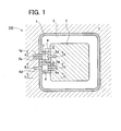
- a semiconductor apparatus 100 in a first exemplary embodiment has a structure as shown in a plan view in Fig. 1 .
- Same reference numerals as the components of the conventional semiconductor apparatus shown in Fig. 16 represent identical functions.
- the semiconductor apparatus 100 comprises a low potential reference circuit region 1 and a high potential reference circuit region 2, and the high potential reference circuit region 2 is surrounded by a high withstand voltage separating region 3, which is known as resurf structure.
- a high withstand voltage separating region 3 By this high withstand voltage separating region 3, the low potential reference circuit region 1 and high potential reference circuit region 2 are separated from each other.
- a trench 4 is formed at the outer periphery of the high withstand voltage separating region 3.
- the trench 4 is filled up with insulating material such as silicon oxide.
- the high potential reference circuit region 2 is isolated from the low potential reference circuit region 1.
- Parts of the high withstand voltage separating region 3 are partitioned by the trench 4.
- a high withstand voltage NMOS 5 and a high withstand voltage PMOS 6 are provided in the partitioned areas.
- Such MOS is intended to transmit signal (shift level) between the low potential reference circuit region 1 and high potential reference circuit region 2. More specifically, for level shifting from the low potential reference circuit region 1 to the high potential reference circuit region 2, the high withstand voltage NMOS 5 having a drain wiring 5d disposed on the high potential reference circuit region 2 is used.
- the high withstand voltage PMOS 6 having a drain wiring 6d disposed on the low potential reference circuit region 1 is used.
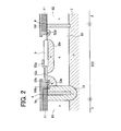
- Fig. 2 is a sectional view of A-A in the semiconductor apparatus 100 shown in Fig. 1 . That is, it is a sectional view of the high withstand voltage NMOS 5.
- the high withstand voltage NMOS 5 is formed in an area partitioned by the trench 4, out of N type epitaxial layers (low potential reference N type layer 81, high potential reference N type layer 82, and in-NMOS drift layer 85) formed on a P - type substrate 7.
- the high withstand voltage NMOS 5 includes gate poly silicon 50g, gate oxide film 50x, source N + region 50s, drain N + region 50d, body P - region 50b, and body contact P + region 50bc.
- Fig. 3 is a sectional view of B-B in the semiconductor apparatus 100 shown in Fig. 1 . That is, it is a sectional view of the high withstand voltage PMOS 6.
- the high withstand voltage PMOS 6 is also formed in an area partitioned by the trench 4, out of N type epitaxial layers (low potential reference N type layer 81, high potential reference N type layer 82, and in-PMOS N type layer 86) formed on the P - type substrate 7.
- the high withstand voltage PMOS 6 includes gate poly silicon 60g, gate oxide film 60x, source P + region 60s, drain P + region 60d, and sub contact N + region 60sc.
- drift P - region 60dr formed in a same diffusion layer as the resurf P - region 50r in the high withstand voltage NMOS 5. Moreover, same as in the high withstand voltage NMOS 5, field oxide film 9, separation-purpose P + diffusion region 10, and others are provided. As shown in Fig. 1 , gate wiring 6g (not shown in Fig. 3 ), source wiring 6s, and drain wiring 6d are provided for shifting the level. In the high withstand voltage PMOS 6 having such structure, by application of voltage to the gate poly silicon 60g, a channel effect is produced in the in-PMOS N type layer 86, and thereby the conduction between the source P + region 60s and drain P + region 60d is controlled.
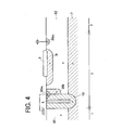
- Fig. 4 is a sectional view of C-C in the semiconductor apparatus 100 shown in Fig. 1 . That is, it is a sectional view of the high withstand voltage separating region 3.
- the high withstand voltage separating region 3 is similar to the high withstand voltage NMOS 5, except that the trench 4 and gate poly silicon 50g at the side of the high potential reference circuit region 2 are not needed.
- the P type diffusion regions 30b, 30bc in the high withstand voltage separating region 3 respectively correspond to the body P - region 50b and body contact P + region 50bc in the high withstand voltage NMOS 5.
- the N type diffusion region 30sc corresponds to the sub contact N + region 60sc in the high withstand voltage PMOS 6.
- the surface potential distribution is designed to be nearly identical with that in the high withstand voltage NMOS 5 and high withstand voltage PMOS 6.
- Fig. 5 is a sectional view of D-D in the semiconductor apparatus 100 shown in Fig. 1 . That is, it is a sectional view of the high withstand voltage NMOS 5 orthogonal to the section in Fig. 2 .
- the high withstand voltage NMOS 5 is surrounded by the trench 4, and the bottom of the trench 4 reaches up to the P - type substrate 7. Accordingly, the in-NMOS drift layer 85 is electrically isolated from the separating region N type layer 83, as well as the low potential reference N type layer 81 and high potential reference N type layer 82.
- the high withstand voltage NMOS 5 and high withstand voltage PMOS 6 are disposed in a region where the high withstand voltage separating region 3 is partitioned by the trench 4.
- high potential drain wiring 5d of high withstand voltage NMOS 5 does not straddle over low potential portion.
- low potential drain wiring 6d of high withstand voltage PMOS 6 does not straddle over high potential portion.
- the high withstand voltage NMOS 5 is completely separated from the high potential reference circuit region 2 by the trench 4.
- the withstand voltage between the drain wiring 5d and substrate is determined by the depth of the trench 4.
- the withstand voltage between the drain N + region 50d and high potential reference N type layer 82 is determined by the width of the trench 4. Hence, required withstand voltage can be realized by the size of the trench 4.
- the width of the trench 4 in the semiconductor apparatus 100 of the embodiment is smaller. Accordingly, as compared with the semiconductor apparatus in Patent Document 2, area loss is smaller.
- the width 2L of the P type slit region must satisfy at least the following formula (1) in order to assure the withstand voltage corresponding to the punch-through breakdown, for the apparatus of Patent Document 2.
- ⁇ is dielectric constant of silicon
- V PT is withstand voltage relative to punch-through breakdown
- q is electric charge of electron
- N P concentration of P type substrate.
- a film thickness may be selected so as to be 3 MV/cm or less. It is enough at about 170 nm to obtain a withstand voltage of 50 V. Hence, as compared with the semiconductor apparatus in Patent Document 2, area loss is smaller.
- the trench 4 since the trench 4 is formed, number of processes is increased as compared with the conventional semiconductor apparatus. However, by applying the trench 4 in separation from other circuits of bipolar transistor and/or CMOS installed in the semiconductor apparatus 100, chip area can be saved substantially. Hence, total cost can be rather lowered.
- other circuits of CMOS and so on are mounted on the N type epitaxial layer formed on the P - type substrate 7 of high resistance. Accordingly, the thickness of this N type epitaxial layer is designed so as to assure a thickness not to cause punch-through breakdown between the P type well region for CMOS and P - type substrate 7 or between P type base region for bipolar transistor and P - type substrate 7.
- the thickness of the N type epitaxial layer is required to be 25 ⁇ m or more.
- the width of the region is required to be 15 ⁇ m or more along with spread in the width direction.
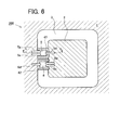
- a semiconductor apparatus 200 in a second exemplary embodiment has a structure as shown in a plan view in Fig. 6 .
- the semiconductor apparatus 200 comprises a low potential reference circuit region 1 and a high potential reference circuit region 2, and the high potential reference circuit region 2 is surrounded by a high withstand voltage separating region 3 same as in the semiconductor apparatus 100 in the first exemplary embodiment. Further, trenches 41, 42 are formed in part of the high withstand voltage separating region 3, and the high withstand voltage separating region 3 is partitioned into plural regions.
- a high withstand voltage NMOS 5 and high withstand voltage PMOS 6 are provided in the partitioned areas.
- the trenches 41, 42 do not surround completely high withstand voltage NMOS 5 and high withstand voltage PMOS 6, respectively. More specifically, trenches are not formed at the source wiring sides. Still more, no trench is formed at the outer periphery of the high withstand voltage separating region 3.
- Fig. 7 is a sectional view of E-E in the semiconductor apparatus 200 shown in Fig. 6 . It is a sectional view of high withstand voltage NMOS 5.
- the high withstand voltage NMOS 5 is formed in N type epitaxial layers (lowpotential referenceNtype layer 81, high potential reference N type layer 82, and in-NMOS drift layer 85) disposed on a P - type substrate 7.
- trench 41 is not present at the side of source wiring 5s.
- the low potential reference N type layer 81 and in-NMOS drift layer 85 are separated by separation-purpose P + diffusion region 12 of which bottom reaches up to the P - type substrate 7. Hence, potential of the P - type substrate 7 is set.
- the in-NMOS drift layer 85 and high potential reference N type layer 82 are separated by means of the trench 41. Further, of the trench 41, by disposing the left end in Fig. 6 at the left side of the source N + region 50s or more left, the high potential reference region 2 and high withstand voltage NMOS 5 are isolated. Hence, leak current or punch-through breakdown does not occur between the high withstand voltage NMOS 5 and high potential reference circuit region 2. Further, as compared with the semiconductor apparatus 100 in the first exemplary embodiment, the total trench volume is smaller. Hence, the yield is higher in fabrication of trenches.
- a semiconductor apparatus 300 in a third exemplary embodiment has a structure as shown in a plan view in Fig. 8 .
- the semiconductor apparatus 300 comprises a low potential reference circuit region 1 and a high potential reference circuit region 2, and the high potential reference circuit region 2 is surrounded by a high withstand voltage separating region 3 same as in the semiconductor apparatus 100 in the first exemplary embodiment. Further, a high withstand voltage NMOS 5 is provided in part of the high withstand voltage separating region 3. An outer wall trench 43 and an inner wall trench 44 are also provided.
- the semiconductor apparatus 300 of this embodiment unlike the semiconductor apparatus 100 in the first exemplary embodiment, does not have trench for partitioning the high withstand voltage separating region 3. It is hence effective to prevent lowering of withstand voltage due to crystal defects or the like likely to occur near the trench.
- the drain N + region of the high with stand voltage NMOS 5 and high potential reference N type layer are not separated, but they are connected electrically. Furthermore, if a plurality of high withstand voltage NMOS 5 or high withstand voltage PMOS 6 are provided in the high withstand voltage separating region 3, they cannot be separated. To solve such problem, in the semiconductor apparatus 300 of this embodiment, an inner wall trench 44 is provided for completely surrounding the high potential reference circuit region 2.
- the drain N + region of the high withstand voltage NMOS 5 and high potential reference N type layer are isolated from each other. Further, a parasitic resistance of the high withstand voltage separating region 3 is generated along the inner wall trench 44.
- the potential of the N + region 50d which is in the high withstand voltage separating region 3 and is near the high potential reference circuit region 2, is taken at position 13.
- the parasitic resistance between this position 13 and the N + region 50d (drain N + region) of the high withstand voltage NMOS 5 is a composite resistance of parasitic resistance route 38 and parasitic resistance route 39 in Fig. 8 . Therefore, they can be disposed by disposing far from each other sufficiently, and the resistance value can be increased, so that effects of leak current can be decreased.
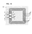
- a semiconductor apparatus 400 in a fourth exemplary embodiment has a structure as shown in a plan view in Fig. 10 .
- the semiconductor apparatus 400 comprises a low potential reference circuit region 1 and a high potential reference circuit region 2, and the high potential reference circuit region 2 is surrounded by a high withstand voltage separating region 3.
- the high withstand voltage separating region 3 By this high withstand voltage separating region 3, the low potential reference circuit region 1 and high potential reference circuit region 2 are separated from each other.
- a trench group 40 in a loop form conforming to the shape of the high withstand voltage separating region 3 is formed.
- Each trench in the trench group 40 is filled with insulating material, and has capacitor structure.
- the high withstand voltage separating region 3 has portions partitioned by the trench 4, and in these partitioned portions, high withstand voltage NMOS 5 and high withstand voltage PMOS 6 for level shift are provided.
- Fig. 11 is a sectional view of F-F of the semiconductor apparatus 400 shown in Fig. 10 .
- the semiconductor apparatus 400 of this embodiment has an SOI structure, and includes an embedded insulating layer 75 formed between the P + type substrate 7 and epitaxial layers (lowpotential reference N type layer 81, high potential reference N type layer 82, and separating region N type layer 83). That is, the P + type substrate 7 and epitaxial layer are insulated by the embedded insulating layer 75.
- the substrate positioned beneath the embedded insulating layer 75 may be either P type or N type.
- the separating region N type layer 83 is partitioned into plural regions by the trench group 40 the bottom of which reaches the embedded insulating layer 75.
- the region closest to the low potential reference circuit region 1 includes P type diffusion regions 30b, 30bc corresponding respectively to the body P - region 50b and body contact P + region 50bc in the high withstand voltage NMOS 5 (see Fig. 12 ).
- the region closest to the high potential reference circuit region 2 includes N type diffusion region 30d corresponding to drain N + region 50d in the high withstand voltage NMOS 5.
- the P type diffusion regions 30b, 30bc are equal in potential to the ground, and the N type diffusion region 30d is equal to the power source of the high potential reference circuit region 2.
- Potential of the main surface elevates step by step from the low potential reference circuit region 1 toward the high potential reference circuit region 2 by the effect of parasitic capacity coupling generated by the trench group 40.
- the coupling ratio of the parasitic capacity can be adjusted by the width of each trench in the trench group 40 at the stage of design.
- Fig. 12 is a sectional view of G-G in the semiconductor apparatus 400 shown in Fig. 10 . It is a sectional view of high withstand voltage NMOS 5.
- the high withstand voltage NMOS 5 is formed in a position partitioned by the trench group 40 and trench 4, out of the N type epitaxial layers formed on the P + type substrate 7.
- the high withstand voltage NMOS 5 includes gate poly silicon 50g, gate oxide film 50x, source N + region 50s, drain N + region 50d, body P - region 50 b, and body contact P + region 50bc.
- in-NMOS drift layer 85 functioning as drift layer is provided on the P + type substrate 7.
- a resurf P - region 50r is formed above the in-NMOS drift layer 85.
- a depletion layer is formed from the PN junction of the separating region N type layer 83 and resurf P - region 50r, so that a higher withstand voltage is realized.
- the potential of the main surface elevates almost linearly between the source and drain.
- Fig. 13 is a sectional view of H-H in the semiconductor apparatus 400 shown in Fig. 10 . It is a sectional view of high withstand voltage PMOS 6.
- the high withstand voltage PMOS 6 also, is formed in a region partitioned by the trench group 40 and trench 4, out of the N type epitaxial layers formed on the P + type substrate 7.
- the high withstand voltage PMOS 6 includes gate poly silicon 60g, gate oxide film 60x, source P + region 60s, drain P + region 60d, and sub contact N + region 60sc. Further, a drift P - region 60dr is formed in the same diffusion layer as the resurf P - region 50r of the high withstand voltage NMOS 5. When a high voltage is applied between the source and drain, the potential of the main surface elevates almost linearly between the source and drain.
- the high withstand voltage NMOS 5 and the high withstand voltage PMOS 6 are disposed in regions where the high withstand voltage separating region 3 is partitioned by the trench 4, and that the trench group 40 of loop form is formed in the high withstand voltage separating region 3.
- potential of the main surface elevates gradually from the low potential reference circuit region 1 toward the high voltage reference circuit region 2. That is, in the semiconductor apparatus 400 of the embodiment, the electric field distribution is similar at any position in the high withstand voltage separating region 3.
- the high potential drain wiring 5d in the high withstand voltage NMOS 5 does not straddle over low potential position.
- the low potential drain wiring 6d in the high withstand voltage PMOS 6 does not straddle over the high potential position. Therefore, as compared with the conventional semiconductor apparatus, lowering of withstand voltage is suppressed and concentration of electric field is also suppressed in a simple structure.
- a semiconductor apparatus 500 in a fifth exemplary embodiment has a structure as shown in a plan view in Fig. 14 . That is, the semiconductor apparatus 500 comprises a low potential reference circuit region 1 and a high potential reference circuit region 2.
- the high potential reference circuit region 2 is surrounded by a plurality of high withstand voltage NMOS 5 (or high withstand voltage PMOS 6). Each high withstand voltage NMOS 5 is surrounded by a trench 4.
- the semiconductor apparatus 500 of the embodiment has the following features. That is, in the separating region between the low potential reference circuit region 1 and high potential reference circuit region 2, potential distribution is uniform. In the semiconductor apparatus 400 in the fourth exemplary embodiment (see Fig. 10 ), both potential distribution in the high withstand voltage separating region 3 (see Fig. 11 ) and potential distribution in the high withstand voltage NMOS 5 (see Fig. 12 ) elevate gradually, but there is a slight difference. As a result, there can be a case where a problem of withstand voltage may occur. By contrast, in the semiconductor apparatus 500 of the embodiment, although undesired high withstand voltage NMOS 5 is contained, the potential distribution is nearly uniform at any position, and there is no problem of withstand voltage or electric field concentration. Incidentally, undesired high withstand voltage NMOS 5 causes no inconvenience by turning off the gate.
- a semiconductor apparatus 600 in a sixth exemplary embodiment has a structure as shown in a plan view in Fig. 15 . That is, the semiconductor apparatus 600 comprises a lowpotential reference circuit region 1 and a high potential reference circuit region 2.
- the high potential reference circuit region 2 is surrounded by a trench 4.
- the trench 4 is filled with insulating material. That is, the region between the low potential reference circuit region 1 and high potential reference circuit region 2 is filled with insulating material.
- high withstand voltage NMOS 5 or high withstand voltage PMOS 6 for level shift is provided.
- potential in the portion of the trench 4 elevates linearly from the low potential reference circuit region 1 toward the high potential reference circuit region 2.
- potential distribution is nearly uniform at any position same as in the fifth exemplary embodiment, and it is free from problem of withstand voltage.
- the width can be narrowed in the positions other than the positions adjacent to the high withstand voltage NMOS 5 or high withstand voltage PMOS 6 of the trench 4.
- the chip area can be saved substantially.
- about 0.1 ⁇ m/V is needed near high withstand voltage MOS, that is, about 100 ⁇ m is needed at withstand voltage of 1000 V, but in other positions, only about 3 ⁇ 10 -3 ⁇ m/V is needed, that is, 3 ⁇ m is enough at withstand voltage of 1000V.
- the high withstand voltage separating region 3 is provided between the low potential reference circuit region 1 and high potential reference circuit region 2. Further, at the outer periphery of the high withstand voltage separating region 3, the trench 4 is formed so that its bottom reach the P - type substrate 7, and the low potential reference circuit region 1 and high potential reference circuit region 2 are completely separated from each other. Further, the high withstand voltage separating region 3 is partitioned by the trench 4, and the high withstand voltage NMOS 5 and high withstand voltage PMOS 6 are provided in partitioned positions. The drain wiring 5d of the high withstand voltage NMOS 5 is formed on the surface of the semiconductor device so as to straddle over the trench 4.
- the drain wiring 5d does not straddle over the high withstand voltage separating region 3, and it is free from effects of drain wiring 5d which is high in potential (low potential in high withstand voltage PMOS 6).
- each high withstand voltage MOS and the low potential reference circuit region 1 and high potential reference circuit region 2 are completely insulated, leak current does not occur, and meander portion for increasing the parasitic resistance is not required.
- the withstand voltage can be adjusted by the size of the trench 4, if the required voltage is different, it can be easily satisfied in the designing stage. That is, the degree of freedom of design is high. Therefore, in the semiconductor apparatus combining the low potential reference circuit and high potential reference circuit, the level can be shifted between the low potential reference circuit and high potential reference circuit, and a compact semiconductor apparatus excellent in withstand voltage is realized.
- the semiconductor apparatus 200 of the second exemplary embodiment no trench is formed in the wall of the source wiring side or outer wall of the high withstand voltage separating region. Therefore, the yield is enhanced, and the semiconductor apparatus is formed in a compact design.
- the semiconductor apparatus 300 of the third exemplary embodiment there is no trench for partitioning the high withstand voltage separating region 3 and high withstand voltage NMOS 5. Hence, it prevents lowering of withstand voltage due to crystal defects or the like likely to occur near the trench.
- the trench group 40 in loop form is formed in the high withstand voltage separating region 3. Accordingly, potential of the main surface in the high withstand voltage separating region 3 elevates slowly from the low potential reference circuit region 1 toward the high potential reference circuit region 2, and the problem of concentration of electric field is alleviated.
- the high potential reference circuit region 2 is surrounded by the high withstand voltage MOS. As a result, in the region between the low potential reference circuit region 1 and high potential reference circuit region 2, the potential distribution is nearly uniform at any position, and it is free from problem of withstand voltage in the separating region.
- the region between the low potential reference circuit region 1 and high potential reference circuit region 2 is filled up with insulating material.
- potential distribution is nearly uniform at any position of the region filled with insulating material, and it is free from problem of with stand voltage in the separating region.
- the semiconductor regions may be exchanged between P type and N type.
- the semiconductor is not limited to silicon, but other semiconductors may be used as well (SiC, GaN, GaAs, etc.).
- the semiconductor apparatus of the invention has a relay semiconductor element in a high withstand voltage separating region, and the output wiring of the relay semiconductor element is disposed so as to straddle over an insulating partition wall. It is hence free from effects of output wiring which is high in potential.
- the relay semiconductor element is insulated from other circuit regions. Hence, measure against leak current such as a meander portion is not needed. Therefore, the invention presents a semiconductor apparatus combining a low potential reference circuit and high potential reference circuit, in which the level can be shifted between the lowpotential reference circuit and high potential reference circuit, and a compact semiconductor apparatus excellent in withstand voltage is realized.
Landscapes
- Element Separation (AREA)
- Metal-Oxide And Bipolar Metal-Oxide Semiconductor Integrated Circuits (AREA)
- Thin Film Transistor (AREA)
- Semiconductor Integrated Circuits (AREA)
Description
- The present invention relates to a semiconductor apparatus in which both a low potential reference circuit and a high potential reference circuit are incorporated. More particularly, it relates to a semiconductor apparatus equipped with high withstand voltage MOS which transmits signals between a low potential reference circuit and a high potential reference circuit.
- There have conventionally and widely been used semiconductor apparatuses in which both a low potential reference circuit and a high potential reference circuit are incorporated for power apparatuses and the like. A semiconductor apparatus of this kind is generally structured such as shown in
FIG. 16 . That is, the semiconductor apparatus has a low potentialreference circuit region 1 and a high potentialreference circuit region 2, and the high potentialreference circuit region 2 is surrounded by a high withstandvoltage separating region 3 formed with resurf structure or the like. Furthermore, there are arranged highwithstand voltage NMOS 5 and highwithstand voltage PMOS 6 for signal transmission (level shift) between the low potentialreference circuit region 1 and the high potentialreference circuit region 2. To be specific, the highwithstand voltage NMOS 5 arranged in the low potentialreference circuit region 1 is used for level shift from the low potentialreference circuit region 1 to the high potentialreference circuit region 2. On the other hand, for level shift from the high potentialreference circuit region 2 to low potentialreference circuit region 1, the highwithstand voltage PMOS 6 arranged in the high potentialreference circuit region 2 is used. Drain wirings of the highwithstand voltage NMOS 5 and the highwithstand voltage PMOS 6 are drawn out to a region of output side from its input side crossing over the high withstandvoltage separating region 3. -
FIG. 17 shows an example of a circuit which conducts level shift from the low potentialreference circuit region 1 to the high potentialreference circuit region 2. This circuit has ahigh withstand NMOS 5, a pull-up resistor 101, and a Zenerdiode 102. Along ON/OFF of the highwithstand voltage NMOS 5, there is caused a potential difference at the drain which corresponds to power voltage in a high potentialreference circuit region 2. Thereby, level shift is conducted between the low potentialreference circuit region 1 and the high potentialreference circuit region 2. For example, suppose that power voltages of both the low potentialreference circuit region 1 and the high potentialreference circuit region 2 are 15V and potential difference between the low potentialreference circuit region 1 and the high potentialreference circuit region 2 is 1000V. In this case, a signal voltage of which is swung between 0V and 15V in the low potentialreference circuit region 1 is converted to a signal swinging between 1000V and 1015V through the circuit ofFIG. 17 . Thereby, a signal transmitted from the low potentialreference circuit region 1 is usable within the high potentialreference circuit region 2. - In a semiconductor apparatus which thus conducts level shift between the low potential
reference circuit region 1 and the high potentialreference circuit region 2, a signal is transmitted through metal wirings (drain wirings) formed on its surface. Drain wirings cross over the low potentialreference circuit region 1, high withstandvoltage separating region 3 and the like, and there is an interlayer dielectric in between. In this case, potential difference between drain wirings (high potential) and the surface of the semiconductor device (lowpotential) is large. As a result, withstand-ability against voltage lowers due to drain wirings. Usually, interlayer dielectric between drain wirings and the surface of the semiconductor device is formed thick for resolving the above-mentioned problem. However, in case of a semiconductor apparatus of which potential difference between a high potential reference circuit region and a low potential reference circuit region exceeds 600V, it leads complication of wiring process due to thickened interlayer dielectric, cost-up, and the like. - As technology to resolve the above-mentioned problem,
Patent Document 1, for example, discloses a semiconductor apparatus in which a high withstand voltage separating region and drift layer of a high withstand MOS for level shift are formed as a package and a drain is formed in a circuit region at output side. In this document, it is stated that level shift can be done without causing a problem regarding withstand-ability of voltage, since drain wirings are wired without crossing over a high withstand voltage separating region or a low potential reference circuit region. - Furthermore, in addition to the above,
Patent Document 2, for example, discloses a semiconductor apparatus in which a portion of an N type high withstand voltage separating region is partitioned with a P type slit region and a high withstand voltage NMOS for level shift is formed at the partitioned portion. That is, N type drain region of a high withstand voltage NMOS and N type layer within a high potential reference circuit region are made to face each other sandwiching a P type slit region. Furthermore, drain wirings of high potential are arranged above the slit region. In this semiconductor apparatus, the slit region is pinched off (depletion regions formed with both of N type layers are incorporated into one). By pinching off the slit region, a surface of the P type slit region has potential almost same as N type layers at its both sides. It is stated that influence of drain wirings is restrained thereby. - Furthermore, in addition to the above,
Patent Document 3, for example, discloses a semiconductor apparatus of SOI structure. This semiconductor apparatus is provided with an insulating region which extends from the main surface of semiconductor apparatus to the buried insulating layer and with a drain wiring above the insulating region. It is stated that influence of drain wirings is restrained because intervals of drain wirings (high potential) and semiconductor layer can be made large. - [Patent Document 1]
JP Laid-open Patent Publication No. 9-55498 - [Patent Document 2]
JP Laid-open Patent Publication No. 9-283716 - [Patent Document 3]
JP Patent Publication No. 3201719 - The above-referenced documents disclose inventions to prevent potential difference between drain wirings and a surface of a semiconductor device frombeing large when level shift is done. However, semiconductor apparatuses in the above-reference documents have had following problems.
- That is, regarding the semiconductor apparatus of
Patent Document 1, in case high withstand voltage MOS is an NMOS, N drain layer of the NMOS is formed in contact with N type layer of the high potential reference circuit region. Therefore, the N drain layer of the high withstand voltage NMOS and N type layer of the high potential reference circuit region are electrically connected to each other. Therefore, there is required a system to enlarge parasitic resistance between the N drain layer of the high withstand voltage NMOS and the N type layer in the high potential reference circuit region. For that reason, in the semiconductor apparatus of thePatent Document 1, the high withstand voltage separating region is bent toward the low potential reference circuit region to form the high withstand voltage NMOS on the bent portion. That is, parasitic resistance is made large by making a distance between the N drain layer of the high withstand voltage NMOS and the N type layer in the high potential reference circuit region long. However, bending the high withstand voltage separating region leads to increase of chip area, which is obstacle to miniaturization of a substrate, as entirety. Furthermore, since it is impossible to completely insulate the N drain layer of the high withstand NMOS and the N type layer in the high potential reference circuit region, leak current is inevitable. Therefore, excessive power consumption occurs. - Furthermore, in the semiconductor apparatus of
Patent Document 2, positioning of N drain layer of the high withstand voltage NMOS and N type layer in the high potential reference circuit region is intended to generate depletion layer between those N type layers. However, in case distance between the two N type layers is too short, punch-through breakdown occurs between N drain layer of the high withstand voltage NMOS and N type layer in the high potential reference circuit region. That is, distance between the two N type layers must be determined taking trade-off relation of voltage withstand-ability and punch-through breakdown into consideration. Therefore, the trade-off relation is not always satisfied depending on required specification voltage and specification voltage restricts the trade-off balance. - Furthermore, as to a semiconductor apparatus disclosed in
Patent Document 3, thickness of an insulating region formed below drain wiring must be made thick.Patent Document 3 describes that the insulating region is formed by means of LOCOS method (localized oxidation of silicon method). However, thickness of oxidation film feasible with LOCOS method is of about 1 to 2µm. Accordingly, the LOCOS method is not applicable to high withstand voltage type devices. Furthermore, other than LOCOS method, there can be conceived of another method that a trench is formed at semiconductor layer and oxide film or poly crystal silicon layer is embedded inside the trench. However, with this method, thickening the insulating region is not sufficient for enhancing voltage withstand-ability between drain wiring and the semiconductor layer, and width of the insulating layer must be taken wide to some extent. In this connection, in case a wide trench exceeding 2µm is formed, it is difficult to fill the trench with oxide film or poly crystal silicon film inside, which lacks feasibility. Furthermore, in the semiconductor apparatus ofPatent Document 3, the semiconductor layer constituting devices is separated by the insulating region. Therefore, potential distribution gets uneven at the border portion of the semiconductor region and the insulating region and electric field is likely to concentrate at the border. - The present invention has been made to resolve problems the above-mentioned conventional semiconductor apparatuses have had. That is, the present invention intends to provide a semiconductor apparatus incorporating both low potential reference circuits and high potential reference circuits, capable of conducting level shift between 7 the low potential reference circuits and high potential reference circuits and excellent in compact design and voltage withstand-ability.
- From
document GB 2 310 081 A - Further, document
US 2002/0043699 A1 discloses a semiconductor device that improves resistance to latch-up and stabilizes breakdown voltage characteristic. Specifically, a first gate electrode and a second drain electrode are linear electrodes having a length not exceeding the length of a source electrode. An isolation region is disposed on both end portions of these electrodes. The region surrounded by two isolation regions and the source electrode becomes a P channel MOS region where a P channel MOS transistor is to be formed. The isolation region has a multi-trench structure that a plurality of trenches are provided in a P type impurity region disposed so as to be rectangle as viewed in plan configuration. Each trench is filled with a conductor such as polysilicon, and the filled conductor is disposed so that it makes no electrical contact with any specific part. - To resolve the above-described problems, according to a first aspect of the present invention, there is provided a semiconductor apparatus containing a low potential reference circuit region and a high potential reference circuit region in accordance with
claim 1. - In the inventive semiconductor apparatus, the high withstand voltage separating region partitions regions for low and high potential reference circuits. In the high withstand voltage separating region, there is arranged a relay semiconductor device for conducting level shift between the low and high potential reference circuits. Output wiring of the relay semiconductor device is wired to a circuit region of output side bridging over the insulating partition. That is, in case of a relay semiconductor device for level shift from a low potential reference circuit to a high potential reference circuit, a surrounding insulating partition is provided between a region for a high potential reference circuit and the relay semiconductor device. Also, in case of a relay semiconductor device for level shift from a high potential reference circuit to a low potential reference circuit, an further surrounding insulating partition is provided between a region for a low potential reference circuit and the relay semiconductor device. Thereby, the output wiring of the relay semiconductor device does not bridge over surface of semiconductor region which has large gap in potential. Accordingly, the semiconductor region is not influenced by the potential of output wiring. Furthermore, the insulating partition prevents punch- through between the relay semiconductor device and the circuit region of output side. Furthermore, since voltage withstand-ability can be adjusted by changing size of an insulating partition, design can be changed easily even if required voltage differs.
- Furthermore, it is preferable that, the semiconductor apparatus according to the first aspect of the present invention further comprises a substrate region arranged below the low and high potential reference circuit regions, wherein bottom portion of the insulating partition extends to the substrate region. Aspects of the invention define advantages of the invention within the scope of
claim 1. Alternatively, it is also preferable the semiconductor apparatus according to the first aspect of the present invention further comprises: a substrate region arranged below the low and high potential reference circuit regions; and an insulating layer embedded between the low and high potential reference circuit regions and the substrate region, the insulating layer electrically insulating the low and high potential reference circuit regions from the substrate region, wherein bottom portions of the insulating partitions extend to the insulating layer. Thereby, the relay semiconductor device is insulated from the low and high potential reference circuits, and occurrence of leak current is prevented. Therefore, it is not required to provide meander portion for enhancing parasitic resistance, which realizes miniaturization of an entirety of a semiconductor apparatus. - Furthermore, it is also preferable that the semiconductor apparatus according to the first aspect of the present invention further comprises a group of insulating partitions arranged between the low and high potential reference circuit regions, the group of insulating partitions dividing space between the low and high potential reference circuit regions into plural regions. Thereby, potential on the main surface in the high withstand voltage separating region elevates gradually from the low potential reference circuit region toward the high potential reference circuit region. Accordingly, a problem of field concentration is relaxed.
- According to a second aspect of the present invention, there is provided a semiconductor apparatus containing a low potential reference circuit region and a high potential reference circuit region between which signals are transmitted, the semiconductor apparatus comprising relay semiconductor devices for transmitting signals between the low and high potential reference circuit regions, each relay semiconductor device being surrounded with an insulating partition filled with insulating material in a trench, wherein the relay semiconductor devices are arranged to form a ring shape which separates the low and high potential reference circuit regions, and output wiring of each relay semiconductor device is wired to an output one of the low and high potential reference circuit regions bridging over the insulating partition. With this inventive semiconductor apparatus also, punch-through and leak current are avoided between the relay semiconductor device and the circuit region of output side. Furthermore, the low and high potential reference circuits are partitioned with the relay semiconductor devices, potential distribution is constant at any portion of the semiconductor apparatus. Thereby, a problem of field concentration is relaxed.
- Furthermore, according to a third aspect of the present invention, there is provided a semiconductor apparatus comprising: a semiconductor substrate of first conduction type; a first region of second conduction type formed above the semiconductor substrate, the first region constituting a low potential reference circuit region; a second region of second conduction type formed above the semiconductor substrate apart from the first region, the second region constituting a high potential reference circuit region; a third region arranged between the first and second regions, formed in a ring shape surrounding one of the first and second regions, the third region constituting a high withstand voltage terminal region; a fourth region arranged forming an incorporated ring structure together with the third region, the fourth region constituting a relay semiconductor device region for transmitting a signal between the first and second regions; and an insulating partition arranged between at least one of the first and second regions and the fourth region, the insulating partition being filled with insulating material in a trench, wherein output wiring of a relay semiconductor device in the fourth region is wired to an output one of the low and high potential reference circuit regions bridging over the insulating partition.
- Furthermore, according to a fourth aspect of the present invention, there is provided a semiconductor apparatus comprising: a semiconductor substrate of either first or second conduction type; an insulating film formed on the semiconductor substrate; a first region of second conduction type formed on the insulating film, the first region constituting a low potential reference circuit region; a second region of second conduction type formed on the insulating film apart from the first region, the second region constituting a high potential reference circuit region; a third region arranged between the first and second regions, formed in a ring shape surrounding one of the first and second region, the third region constituting a high withstand voltage terminal region; a fourth region arranged forming an incorporated ring structure together with the third region, the fourth region constituting a relay semiconductor device region for transmitting a signal between the first and second region; and an insulating partition arrangedbetween at least one of the first and second regions and the fourth region, the insulating partition being filled with insulating material in a trench, wherein output wiring of a relay semiconductor device in the fourth region is wired to an output one of the low and high potential reference circuit regions bridging over the insulating partition. It is to be noted that the semiconductor substrate is a region of which density is higher in comparison with the first and second regions.
- It is preferable that in the semiconductor apparatus according to the third or fourth aspect of the present invention, bottom portion of the insulating partition extends to either the semiconductor substrate or the insulating film, and the insulating partition surrounds periphery of a relay semiconductor device in the fourth region from at least three directions, or the third region composes junction isolation type structure in which high withstand voltage is maintained by PN junction.
- It is also preferable that, in the semiconductor apparatus according to the third or fourth aspect of the present invention, the third region has insulation isolation type structure in which high withstand voltage is maintained by a plurality of insulating partitions. It is further preferable that, regions partitioned by the insulating partitions have capacitor structure in which the insulating partitions works as dielectric film, and potential elevates gradually from the first region side toward the second region side.
- Furthermore, according to a fifth aspect of the present invention, there is provided a semiconductor apparatus comprising: a semiconductor substrate of first conduction type; a first region of second conduction type formed above the semiconductor substrate, the first region constituting a low potential reference circuit region; a second region of second conduction type formed above the semiconductor substrate apart from the first region, the second region constituting a high potential reference circuit region; a plurality of fourth regions arranged between the first and second regions, formed in a ring shape surrounding one of the first and second regions, the fourth regions constituting relay semiconductor device regions for transmitting signals between the first and second regions; and an insulatingpartition arranged between at least one of the first and second regions and the fourth regions, the insulating partition being filled with insulating material in a trench, wherein output wiring of a relay semiconductor device in a fourth region is wired to an output one of the low and high potential reference circuit region bridging over the insulating partition.
- Furthermore, according to a sixth aspect of the present invention, there is provided a semiconductor apparatus comprising: a semiconductor substrate of either first or second conduction type; an insulating film formed on the semiconductor substrate; a first region of second conduction type formed on the insulating film, the first region constituting a low potential reference circuit region; a second region of second conduction type formed on the insulating film apart from the first region thereon, the second region constituting a high potential reference circuit region; a plurality of fourth regions arranged between the first and second regions, formed in a ring shape surrounding one of the first and second regions, the fourth regions constituting relay semiconductor device regions for transmitting signals between the first and second regions; and an insulating partition arranged between at least one of the first and second regions and the fourth regions, the insulating partition being filled with insulating material in a trench, wherein output wiring of a relay semiconductor device in a fourth region is wired to an output one of the low and high potential reference circuit region bridging over the insulating partition.
-
-
Fig. 1 is a plan view showing structure of a semiconductor apparatus directed to a first exemplary embodiment. -
Fig. 2 is a sectional view showing structure of A-A section of the semiconductor apparatus directed toFig. 1 . -
Fig. 3 is a sectional view showing structure of B-B section of the semiconductor apparatus directed toFig. 1 . -
Fig. 4 is a sectional view showing structure of C-C section of the semiconductor apparatus directed toFig. 1 . -
Fig. 5 is a sectional view showing structure of D-D section of 28/04/2005 the semiconductor apparatus directed toFig. 1 . -
Fig. 6 is a plan view showing structure of a semiconductor apparatus directed to a second exemplary embodiment. -
Fig. 7 is a sectional view showing structure of E-E section of the semiconductor apparatus directed toFig. 6 . -
Fig. 8 is a plan view showing structure of a semiconductor apparatus directed to a third exemplary embodiment. -
Fig. 9 is a plan view showing structure of a trench-less semiconductor apparatus, an applied example of the semiconductor apparatus directed to the third embodiment. -
Fig. 10 is a plan view showing structure of a semiconductor apparatus directed to a fourth exemplary embodiment. -
Fig. 11 is a sectional view showing structure of F-F section of the semiconductor apparatus directed toFig. 10 . -
Fig. 12 is a sectional view showing structure of G-G section of the semiconductor apparatus directed toFig. 10 . -
Fig. 13 is a sectional view showing structure of H-H section of the semiconductor apparatus directed toFig. 10 . -
Fig. 14 is a plan view showing structure of a semiconductor apparatus directed to a fifth exemplary embodiment. -
Fig. 15 is a plan view showing structure of a semiconductor apparatus directed to a sixth exemplary embodiment. -
Fig. 16 is a plan view showing structure of a conventional semiconductor apparatus. -
Fig. 17 shows circuit structure the conventional semiconductor apparatus. - Exemplary embodiments of the invention are specifically described below while referring to the companying drawings, from which only exemplary embodiments third to fifth (3rd-5th) show the application of the invention in power MOS mounted on an electric vehicle, for example.
Embodiments - A
semiconductor apparatus 100 in a first exemplary embodiment has a structure as shown in a plan view inFig. 1 . Same reference numerals as the components of the conventional semiconductor apparatus shown inFig. 16 represent identical functions. Thesemiconductor apparatus 100 comprises a low potentialreference circuit region 1 and a high potentialreference circuit region 2, and the high potentialreference circuit region 2 is surrounded by a high withstandvoltage separating region 3, which is known as resurf structure. By this high withstandvoltage separating region 3, the low potentialreference circuit region 1 and high potentialreference circuit region 2 are separated from each other. Further, atrench 4 is formed at the outer periphery of the high withstandvoltage separating region 3. Thetrench 4 is filled up with insulating material such as silicon oxide. Accordingly, the high potentialreference circuit region 2 is isolated from the low potentialreference circuit region 1. Parts of the high withstandvoltage separating region 3 are partitioned by thetrench 4. A high withstandvoltage NMOS 5 and a high withstandvoltage PMOS 6 are provided in the partitioned areas. Such MOS is intended to transmit signal (shift level) between the low potentialreference circuit region 1 and high potentialreference circuit region 2. More specifically, for level shifting from the low potentialreference circuit region 1 to the high potentialreference circuit region 2, the high withstandvoltage NMOS 5 having adrain wiring 5d disposed on the high potentialreference circuit region 2 is used. On the other hand, for level shifting from the high potentialreference circuit region 2 to the low potentialreference circuit region 1, the high withstandvoltage PMOS 6 having adrain wiring 6d disposed on the low potentialreference circuit region 1 is used. -
Fig. 2 is a sectional view of A-A in thesemiconductor apparatus 100 shown inFig. 1 . That is, it is a sectional view of the high withstandvoltage NMOS 5. The high withstandvoltage NMOS 5 is formed in an area partitioned by thetrench 4, out of N type epitaxial layers (low potential referenceN type layer 81, high potential referenceN type layer 82, and in-NMOS drift layer 85) formed on a P- type substrate 7. The high withstandvoltage NMOS 5 includesgate poly silicon 50g,gate oxide film 50x, source N+ region 50s, drain N+ region 50d, body P- region 50b, and body contact P+ region 50bc. It further includes resurf P- region 50r biased at the same potential (usually 0 V) as the body P- region 50b. Moreover, in-NMOS drift layer 85,field oxide film 9, separation-purpose P+ diffusion region 10, and others are provided. As shown inFig. 1 ,gate wiring 5g (not shown inFig. 2 ),source wiring 5s, anddrain wiring 5d are provided on the surface of thesemiconductor apparatus 100, and the level is shifted by these wirings. An interlayer insulatingfilm 11 is formed between thesewirings voltage NMOS 5 having such structure, by application of voltage to thegate poly silicon 50g, a channel effect is produced in the body P- region 50b, and thereby the conduction between the source N+ region 50s and drain N+ region 50d is controlled. -
Fig. 3 is a sectional view of B-B in thesemiconductor apparatus 100 shown inFig. 1 . That is, it is a sectional view of the high withstandvoltage PMOS 6. The high withstandvoltage PMOS 6 is also formed in an area partitioned by thetrench 4, out of N type epitaxial layers (low potential referenceN type layer 81, high potential referenceN type layer 82, and in-PMOS N type layer 86) formed on the P- type substrate 7. The high withstandvoltage PMOS 6 includesgate poly silicon 60g,gate oxide film 60x, source P+ region 60s, drain P+ region 60d, and sub contact N+ region 60sc. It further includes drift P- region 60dr formed in a same diffusion layer as the resurf P- region 50r in the high withstandvoltage NMOS 5. Moreover, same as in the high withstandvoltage NMOS 5,field oxide film 9, separation-purpose P+ diffusion region 10, and others are provided. As shown inFig. 1 ,gate wiring 6g (not shown inFig. 3 ),source wiring 6s, anddrain wiring 6d are provided for shifting the level. In the high withstandvoltage PMOS 6 having such structure, by application of voltage to thegate poly silicon 60g, a channel effect is produced in the in-PMOSN type layer 86, and thereby the conduction between the source P+ region 60s and drain P+ region 60d is controlled. -
Fig. 4 is a sectional view of C-C in thesemiconductor apparatus 100 shown inFig. 1 . That is, it is a sectional view of the high withstandvoltage separating region 3. Compared with the high withstandvoltage NMOS 5 inFig. 2 , the high withstandvoltage separating region 3 is similar to the high withstandvoltage NMOS 5, except that thetrench 4 andgate poly silicon 50g at the side of the high potentialreference circuit region 2 are not needed. The Ptype diffusion regions 30b, 30bc in the high withstandvoltage separating region 3 respectively correspond to the body P- region 50b and body contact P+ region 50bc in the high withstandvoltage NMOS 5. The N type diffusion region 30sc corresponds to the sub contact N+ region 60sc in the high withstandvoltage PMOS 6. The surface potential distribution is designed to be nearly identical with that in the high withstandvoltage NMOS 5 and high withstandvoltage PMOS 6. -
Fig. 5 is a sectional view of D-D in thesemiconductor apparatus 100 shown inFig. 1 . That is, it is a sectional view of the high withstandvoltage NMOS 5 orthogonal to the section inFig. 2 . The high withstandvoltage NMOS 5 is surrounded by thetrench 4, and the bottom of thetrench 4 reaches up to the P- type substrate 7. Accordingly, the in-NMOS drift layer 85 is electrically isolated from the separating regionN type layer 83, as well as the low potential referenceN type layer 81 and high potential referenceN type layer 82. - It is a feature of the
semiconductor apparatus 100 of the embodiment that the high withstandvoltage NMOS 5 and high withstandvoltage PMOS 6 are disposed in a region where the high withstandvoltage separating region 3 is partitioned by thetrench 4. In thesemiconductor apparatus 100, highpotential drain wiring 5d of high withstandvoltage NMOS 5 does not straddle over low potential portion. And also, lowpotential drain wiring 6d of high withstandvoltage PMOS 6 does not straddle over high potential portion. Hence, there is no problem of withstand voltage. This is same as in the semiconductor apparatus inPatent Document 1 and others, but in thesemiconductor apparatus 100, the high withstandvoltage NMOS 5 is completely separated from the high potentialreference circuit region 2 by thetrench 4. Accordingly, leak current or punch-through breakdown does not occur between the drain N+ region 50d and high potential referenceN type layer 82. Therefore, the meander portion as in the semiconductor apparatus inPatent Document 1 is not needed, and the area loss is suppressed. Differently from the semiconductor apparatus inPatent Document 2, it is not required to consider trade- off between withstand voltage and punch-through breakdown, and limitation of operating voltage is not required. In thesemiconductor apparatus 100 of the embodiment, the withstand voltage between thedrain wiring 5d and substrate is determined by the depth of thetrench 4. The withstand voltage between the drain N+ region 50d and high potential referenceN type layer 82 is determined by the width of thetrench 4. Hence, required withstand voltage can be realized by the size of thetrench 4. - As compared with the width of the P type slit region exposed on the surface in the semiconductor apparatus in
Patent Document 2, the width of thetrench 4 in thesemiconductor apparatus 100 of the embodiment is smaller. Accordingly, as compared with the semiconductor apparatus inPatent Document 2, area loss is smaller. - More specifically, the width 2L of the P type slit region must satisfy at least the following formula (1) in order to assure the withstand voltage corresponding to the punch-through breakdown, for the apparatus of
Patent Document 2.
where "ε"is dielectric constant of silicon, "VPT" is withstand voltage relative to punch-through breakdown, "q" is electric charge of electron, and "NP" is concentration of P type substrate. For example, in the case of punch-through withstand voltage VPT = 50 V, and substrate concentration NP = 1.0 × 1014 cm-3 generally used in high withstand voltage semiconductor apparatus of 1000 V class, 2L ≒ 26µm according to formula (1). - On the other hand, in the
semiconductor apparatus 100 of the embodiment, when using silicon oxide film astrench 4, generally, a film thickness may be selected so as to be 3 MV/cm or less. It is enough at about 170 nm to obtain a withstand voltage of 50 V. Hence, as compared with the semiconductor apparatus inPatent Document 2, area loss is smaller. - In the
semiconductor apparatus 100 of the embodiment, since thetrench 4 is formed, number of processes is increased as compared with the conventional semiconductor apparatus. However, by applying thetrench 4 in separation from other circuits of bipolar transistor and/or CMOS installed in thesemiconductor apparatus 100, chip area can be saved substantially. Hence, total cost can be rather lowered. In particular, in this kind of high withstand voltage semiconductor device, other circuits of CMOS and so on are mounted on the N type epitaxial layer formed on the P- type substrate 7 of high resistance. Accordingly, the thickness of this N type epitaxial layer is designed so as to assure a thickness not to cause punch-through breakdown between the P type well region for CMOS and P- type substrate 7 or between P type base region for bipolar transistor and P- type substrate 7. For example, to mount a circuit of 35V system, generally, the thickness of the N type epitaxial layer is required to be 25µm or more. When separation-purpose P+ diffusion region is formed by thermal diffusion as in the prior art, the width of the region is required to be 15µm or more along with spread in the width direction. Hence, in the method of separating the region by the P+ diffusion region, as compared with the method of separating the region by thetrench 4 as in the embodiment, area loss is greater. Therefore, the use of thetrench 4 does not always lead to elevation of total cost. - A
semiconductor apparatus 200 in a second exemplary embodiment has a structure as shown in a plan view inFig. 6 . Thesemiconductor apparatus 200 comprises a low potentialreference circuit region 1 and a high potentialreference circuit region 2, and the high potentialreference circuit region 2 is surrounded by a high withstandvoltage separating region 3 same as in thesemiconductor apparatus 100 in the first exemplary embodiment. Further,trenches voltage separating region 3, and the high withstandvoltage separating region 3 is partitioned into plural regions. A high withstandvoltage NMOS 5 and high withstandvoltage PMOS 6 are provided in the partitioned areas. What differs from thesemiconductor apparatus 100 in the first exemplary embodiment is that thetrenches voltage NMOS 5 and high withstandvoltage PMOS 6, respectively. More specifically, trenches are not formed at the source wiring sides. Still more, no trench is formed at the outer periphery of the high withstandvoltage separating region 3. -
Fig. 7 is a sectional view of E-E in thesemiconductor apparatus 200 shown inFig. 6 . It is a sectional view of high withstandvoltage NMOS 5. The high withstandvoltage NMOS 5 is formed in N type epitaxial layers (lowpotential referenceNtype layer 81, high potential referenceN type layer 82, and in-NMOS drift layer 85) disposed on a P- type substrate 7. What differs from thesemiconductor apparatus 100 in the first exemplary embodiment is thattrench 41 is not present at the side ofsource wiring 5s. Instead, the low potential referenceN type layer 81 and in-NMOS drift layer 85 are separated by separation-purpose P+ diffusion region 12 of which bottom reaches up to the P- type substrate 7. Hence, potential of the P- type substrate 7 is set. On the other hand, the in-NMOS drift layer 85 and high potential referenceN type layer 82 are separated by means of thetrench 41. Further, of thetrench 41, by disposing the left end inFig. 6 at the left side of the source N+ region 50s or more left, the highpotential reference region 2 and high withstandvoltage NMOS 5 are isolated. Hence, leak current or punch-through breakdown does not occur between the high withstandvoltage NMOS 5 and high potentialreference circuit region 2. Further, as compared with thesemiconductor apparatus 100 in the first exemplary embodiment, the total trench volume is smaller. Hence, the yield is higher in fabrication of trenches. - A
semiconductor apparatus 300 in a third exemplary embodiment has a structure as shown in a plan view inFig. 8 . Thesemiconductor apparatus 300 comprises a low potentialreference circuit region 1 and a high potentialreference circuit region 2, and the high potentialreference circuit region 2 is surrounded by a high withstandvoltage separating region 3 same as in thesemiconductor apparatus 100 in the first exemplary embodiment. Further, a high withstandvoltage NMOS 5 is provided in part of the high withstandvoltage separating region 3. Anouter wall trench 43 and aninner wall trench 44 are also provided. Thesemiconductor apparatus 300 of this embodiment, unlike thesemiconductor apparatus 100 in the first exemplary embodiment, does not have trench for partitioning the high withstandvoltage separating region 3. It is hence effective to prevent lowering of withstand voltage due to crystal defects or the like likely to occur near the trench. - Only for the purpose of preventing lowering of withstand voltage due to crystal defects or the like near the trench, it is realized by a trenchless structure such as
semiconductor apparatus 310 shown inFig. 9 . However, in thesemiconductor apparatus 310, the drain N+ region of the high withstand voltage NMOS 5 and high potential reference N type layer are not separated, but they are connected electrically. Furthermore, if a plurality of high withstandvoltage NMOS 5 or high withstandvoltage PMOS 6 are provided in the high withstandvoltage separating region 3, they cannot be separated. To solve such problem, in thesemiconductor apparatus 300 of this embodiment, aninner wall trench 44 is provided for completely surrounding the high potentialreference circuit region 2. As a result, the drain N+ region of the high withstandvoltage NMOS 5 and high potential reference N type layer are isolated from each other. Further, a parasitic resistance of the high withstandvoltage separating region 3 is generated along theinner wall trench 44. In thesemiconductor apparatus 300 of the embodiment, the potential of the N+ region 50d, which is in the high withstandvoltage separating region 3 and is near the high potentialreference circuit region 2, is taken atposition 13. The parasitic resistance between thisposition 13 and the N+ region 50d (drain N+ region) of the high withstandvoltage NMOS 5 is a composite resistance ofparasitic resistance route 38 andparasitic resistance route 39 inFig. 8 . Therefore, they can be disposed by disposing far from each other sufficiently, and the resistance value can be increased, so that effects of leak current can be decreased. - A
semiconductor apparatus 400 in a fourth exemplary embodiment has a structure as shown in a plan view inFig. 10 . Thesemiconductor apparatus 400 comprises a low potentialreference circuit region 1 and a high potentialreference circuit region 2, and the high potentialreference circuit region 2 is surrounded by a high withstandvoltage separating region 3. By this high withstandvoltage separating region 3, the low potentialreference circuit region 1 and high potentialreference circuit region 2 are separated from each other. Further, within the high withstandvoltage separating region 3, atrench group 40 in a loop form conforming to the shape of the high withstandvoltage separating region 3 is formed. Each trench in thetrench group 40 is filled with insulating material, and has capacitor structure. The high withstandvoltage separating region 3 has portions partitioned by thetrench 4, and in these partitioned portions, high withstandvoltage NMOS 5 and high withstandvoltage PMOS 6 for level shift are provided. -
Fig. 11 is a sectional view of F-F of thesemiconductor apparatus 400 shown inFig. 10 . Thesemiconductor apparatus 400 of this embodiment has an SOI structure, and includes an embedded insulatinglayer 75 formed between the P+ type substrate 7 and epitaxial layers (lowpotential referenceN type layer 81, high potential referenceN type layer 82, and separating region N type layer 83). That is, the P+ type substrate 7 and epitaxial layer are insulated by the embedded insulatinglayer 75. The substrate positioned beneath the embedded insulatinglayer 75 may be either P type or N type. The separating regionN type layer 83 is partitioned into plural regions by thetrench group 40 the bottom of which reaches the embedded insulatinglayer 75. Of the regions partitioned by thetrench group 40, the region closest to the low potentialreference circuit region 1 includes Ptype diffusion regions 30b, 30bc corresponding respectively to the body P- region 50b and body contact P+ region 50bc in the high withstand voltage NMOS 5 (seeFig. 12 ). The region closest to the high potentialreference circuit region 2 includes Ntype diffusion region 30d corresponding to drain N+ region 50d in the high withstandvoltage NMOS 5. The Ptype diffusion regions 30b, 30bc are equal in potential to the ground, and the Ntype diffusion region 30d is equal to the power source of the high potentialreference circuit region 2. Potential of the main surface elevates step by step from the low potentialreference circuit region 1 toward the high potentialreference circuit region 2 by the effect of parasitic capacity coupling generated by thetrench group 40. The coupling ratio of the parasitic capacity can be adjusted by the width of each trench in thetrench group 40 at the stage of design. -
Fig. 12 is a sectional view of G-G in thesemiconductor apparatus 400 shown inFig. 10 . It is a sectional view of high withstandvoltage NMOS 5. The high withstandvoltage NMOS 5 is formed in a position partitioned by thetrench group 40 andtrench 4, out of the N type epitaxial layers formed on the P+ type substrate 7. The high withstandvoltage NMOS 5 includesgate poly silicon 50g,gate oxide film 50x, source N+ region 50s, drain N+ region 50d, body P- region 50 b, and body contact P+ region 50bc. Further, on the P+ type substrate 7, in-NMOS drift layer 85 functioning as drift layer is provided. Above the in-NMOS drift layer 85, a resurf P- region 50r is formed. When a high voltage is applied between the source and drain, a depletion layer is formed from the PN junction of the separating regionN type layer 83 and resurf P- region 50r, so that a higher withstand voltage is realized. Here, the potential of the main surface elevates almost linearly between the source and drain. -
Fig. 13 is a sectional view of H-H in thesemiconductor apparatus 400 shown inFig. 10 . It is a sectional view of high withstandvoltage PMOS 6. The high withstandvoltage PMOS 6, also, is formed in a region partitioned by thetrench group 40 andtrench 4, out of the N type epitaxial layers formed on the P+ type substrate 7. The high withstandvoltage PMOS 6 includesgate poly silicon 60g,gate oxide film 60x, source P+ region 60s, drain P+ region 60d, and sub contact N+ region 60sc. Further, a drift P- region 60dr is formed in the same diffusion layer as the resurf P- region 50r of the high withstandvoltage NMOS 5. When a high voltage is applied between the source and drain, the potential of the main surface elevates almost linearly between the source and drain. - It is a feature of the
semiconductor apparatus 400 of the embodiment that the high withstandvoltage NMOS 5 and the high withstandvoltage PMOS 6 are disposed in regions where the high withstandvoltage separating region 3 is partitioned by thetrench 4, and that thetrench group 40 of loop form is formed in the high withstandvoltage separating region 3. As a result, at any position of the high withstandvoltage separating region 3, high withstandvoltage NMOS 5, and high withstandvoltage PMOS 6, potential of the main surface elevates gradually from the low potentialreference circuit region 1 toward the high voltagereference circuit region 2. That is, in thesemiconductor apparatus 400 of the embodiment, the electric field distribution is similar at any position in the high withstandvoltage separating region 3. Moreover, same as in the semiconductor apparatus in the first exemplary embodiment, the highpotential drain wiring 5d in the high withstandvoltage NMOS 5 does not straddle over low potential position. Also, the lowpotential drain wiring 6d in the high withstandvoltage PMOS 6 does not straddle over the high potential position. Therefore, as compared with the conventional semiconductor apparatus, lowering of withstand voltage is suppressed and concentration of electric field is also suppressed in a simple structure. - A
semiconductor apparatus 500 in a fifth exemplary embodiment has a structure as shown in a plan view inFig. 14 . That is, thesemiconductor apparatus 500 comprises a low potentialreference circuit region 1 and a high potentialreference circuit region 2. The high potentialreference circuit region 2 is surrounded by a plurality of high withstand voltage NMOS 5 (or high withstand voltage PMOS 6). Each high withstandvoltage NMOS 5 is surrounded by atrench 4. - The
semiconductor apparatus 500 of the embodiment has the following features. That is, in the separating region between the low potentialreference circuit region 1 and high potentialreference circuit region 2, potential distribution is uniform. In thesemiconductor apparatus 400 in the fourth exemplary embodiment (seeFig. 10 ), both potential distribution in the high withstand voltage separating region 3 (seeFig. 11 ) and potential distribution in the high withstand voltage NMOS 5 (seeFig. 12 ) elevate gradually, but there is a slight difference. As a result, there can be a case where a problem of withstand voltage may occur. By contrast, in thesemiconductor apparatus 500 of the embodiment, although undesired high withstandvoltage NMOS 5 is contained, the potential distribution is nearly uniform at any position, and there is no problem of withstand voltage or electric field concentration. Incidentally, undesired high withstandvoltage NMOS 5 causes no inconvenience by turning off the gate. - A
semiconductor apparatus 600 in a sixth exemplary embodiment has a structure as shown in a plan view inFig. 15 . That is, thesemiconductor apparatus 600 comprises a lowpotentialreference circuit region 1 and a high potentialreference circuit region 2. The high potentialreference circuit region 2 is surrounded by atrench 4. Thetrench 4 is filled with insulating material. That is, the region between the low potentialreference circuit region 1 and high potentialreference circuit region 2 is filled with insulating material. In the position partitioned by thetrench 4, high withstandvoltage NMOS 5 or high withstandvoltage PMOS 6 for level shift is provided. - In the
semiconductor apparatus 600 of the embodiment, potential in the portion of thetrench 4 elevates linearly from the low potentialreference circuit region 1 toward the high potentialreference circuit region 2. As a result, potential distribution is nearly uniform at any position same as in the fifth exemplary embodiment, and it is free from problem of withstand voltage. The width can be narrowed in the positions other than the positions adjacent to the high withstandvoltage NMOS 5 or high withstandvoltage PMOS 6 of thetrench 4. Hence, the chip area can be saved substantially. Generally, about 0.1µm/V is needed near high withstand voltage MOS, that is, about 100µm is needed at withstand voltage of 1000 V, but in other positions, only about 3 × 10⁻³ µm/V is needed, that is, 3µm is enough at withstand voltage of 1000V. - As described specifically above, in the
semiconductor apparatus 100 of the first exemplary embodiment, the high withstandvoltage separating region 3 is provided between the low potentialreference circuit region 1 and high potentialreference circuit region 2. Further, at the outer periphery of the high withstandvoltage separating region 3, thetrench 4 is formed so that its bottom reach the P- type substrate 7, and the low potentialreference circuit region 1 and high potentialreference circuit region 2 are completely separated from each other. Further, the high withstandvoltage separating region 3 is partitioned by thetrench 4, and the high withstandvoltage NMOS 5 and high withstandvoltage PMOS 6 are provided in partitioned positions. Thedrain wiring 5d of the high withstandvoltage NMOS 5 is formed on the surface of the semiconductor device so as to straddle over thetrench 4. As a result, thedrain wiring 5d does not straddle over the high withstandvoltage separating region 3, and it is free from effects ofdrain wiring 5d which is high in potential (low potential in high withstand voltage PMOS 6). Besides, since each high withstand voltage MOS and the low potentialreference circuit region 1 and high potentialreference circuit region 2 are completely insulated, leak current does not occur, and meander portion for increasing the parasitic resistance is not required. In thesemiconductor apparatus 100, since the withstand voltage can be adjusted by the size of thetrench 4, if the required voltage is different, it can be easily satisfied in the designing stage. That is, the degree of freedom of design is high. Therefore, in the semiconductor apparatus combining the low potential reference circuit and high potential reference circuit, the level can be shifted between the low potential reference circuit and high potential reference circuit, and a compact semiconductor apparatus excellent in withstand voltage is realized. - In the
semiconductor apparatus 200 of the second exemplary embodiment, no trench is formed in the wall of the source wiring side or outer wall of the high withstand voltage separating region. Therefore, the yield is enhanced, and the semiconductor apparatus is formed in a compact design. In thesemiconductor apparatus 300 of the third exemplary embodiment, there is no trench for partitioning the high withstandvoltage separating region 3 and high withstandvoltage NMOS 5. Hence, it prevents lowering of withstand voltage due to crystal defects or the like likely to occur near the trench. - In the
semiconductor apparatus 400 of the fourth exemplary embodiment, thetrench group 40 in loop form is formed in the high withstandvoltage separating region 3. Accordingly, potential of the main surface in the high withstandvoltage separating region 3 elevates slowly from the low potentialreference circuit region 1 toward the high potentialreference circuit region 2, and the problem of concentration of electric field is alleviated. In thesemiconductor apparatus 500 of the fifth exemplary embodiment, the high potentialreference circuit region 2 is surrounded by the high withstand voltage MOS. As a result, in the region between the low potentialreference circuit region 1 and high potentialreference circuit region 2, the potential distribution is nearly uniform at any position, and it is free from problem of withstand voltage in the separating region. In thesemiconductor apparatus 600 of the sixth exemplary embodiment, the region between the low potentialreference circuit region 1 and high potentialreference circuit region 2 is filled up with insulating material. In such embodiment, too, potential distribution is nearly uniform at any position of the region filled with insulating material, and it is free from problem of with stand voltage in the separating region. - The foregoing embodiments are mere examples. Therefore, the invention may be changed and modified within the scope defined in the appended claims. For example, the semiconductor regions may be exchanged between P type and N type. The semiconductor is not limited to silicon, but other semiconductors may be used as well (SiC, GaN, GaAs, etc.).
- The semiconductor apparatus of the invention has a relay semiconductor element in a high withstand voltage separating region, and the output wiring of the relay semiconductor element is disposed so as to straddle over an insulating partition wall. It is hence free from effects of output wiring which is high in potential. By the insulating partition wall, the relay semiconductor element is insulated from other circuit regions. Hence, measure against leak current such as a meander portion is not needed. Therefore, the invention presents a semiconductor apparatus combining a low potential reference circuit and high potential reference circuit, in which the level can be shifted between the lowpotential reference circuit and high potential reference circuit, and a compact semiconductor apparatus excellent in withstand voltage is realized.
Claims (14)
- A semiconductor apparatus containing a low potential reference circuit region (1) and a high potential reference circuit region (2) between which signals are transmitted,
the semiconductor apparatus comprising:a high withstand voltage separating region (3), which is arranged between the low and high potential reference circuit regions (1, 2) so as to surround the high potential reference circuit region (2) and being surrounded by the low potential reference circuit region (1), thereby separating the low and high potential reference circuit regions (1, 2),an outer wall trench (43) and an inner wall trench (44) filled with insulating material, respectively,wherein the inner wall trench (44) is arranged between the high potential reference circuit region (2) and the high withstand voltage separating region (3) so as to surround the high potential reference circuit region (2) and separate said high potential reference circuit region (2) from the high withstand voltage separating region (3), andwherein the outer wall trench (43) is arranged between the high withstand voltage separating region (3) and the low potential reference circuit region (1) so as to surround the high withstand voltage separating region (3) and separated said high withstand voltage separating region (3) from the low potential reference circuit region (1);the semiconductor apparatus further comprising:a relay semiconductor device (5, 6), formed in the high withstand voltage separating region (3), for transmitting a signal from one of the low and high potential reference circuit regions (1, 2) to the other of them; andan insulating partition (4) arranged between the relay semiconductor device (5, 6) and one of the low and high potential reference circuit regions (1, 2) that is at the output one of the relay semiconductor device (5, 6), the insulating partition (4) being filled with insulating material in a trench,wherein input wiring (5s, 6s) and output wiring (5d, 6d) of the relay semiconductor device (5,6) are wired to an input one and an output one of the low and high potential reference circuit regions (1, 2) bridging over the insulating partition (4). - A semiconductor apparatus according to claim 1
further comprising a substrate region (7) arranged below the low and high potential reference circuit regions (1, 2),
wherein the high withstand voltage separating region (3) is formed in said substrate region (7),
a bottom portion of the insulating partition (4) extends to the substrate region (7), and
the insulation partition (4) surrounds the relay semiconductor device (5, 6). - A semiconductor apparatus according to claim 1 or claim 2
further comprising a group of insulating partitions (40) arranged between the low and high potential reference circuit regions (1, 2), the group of insulating partitions (40) dividing space between the low and high potential reference circuit regions (1,2) into plural regions. - A semiconductor apparatus according to claim 1, wherein
a plurality of the relay semiconductor devices (5, 6) are arranged to form a ring shape in the high withstand voltage separating region (3),
each relay semiconductor device (5, 6) is surrounded with the insulating partition (4), and
input wiring (5s, 6s) and output wiring (5d, 6d) of each relay semiconductor device (5, 6) are wired to an input one and an output one of the low and high potential reference circuit regions (1, 2) bridging over the insulating partition (4). - A semiconductor apparatus according to any one of claims 1 to 4 further comprising:
a substrate region arranged below the low and high potential reference circuit regions; and
an insulating layer (75) embedded between the low and high potential reference circuit regions (1, 2) and the substrate region (7), the insulating layer (75) electrically insulating the low and high potential reference circuit regions (1, 2) from the substrate region (7),
wherein bottom portions of the insulating partitions (4) extend to the insulating layer (75) and the insulating partitions (4) surround the relay semiconductor devices (5, 6). - A semiconductor apparatus according to claim 1 comprising:a semiconductor substrate (7) of first conduction type;wherein the low and high potential reference circuit regions (1, 2) are regions of second conduction type formed over a main surface of the semiconductor substrate so that the low potential reference circuit region (1) surrounds the high potential reference circuit region (2) in separated relation, andthe high withstand voltage separating region (3) is a region formed in a ring shape between the low and high potential reference circuit regions (1, 2).
- A semiconductor apparatus according to claim 1 comprising:a semiconductor substrate of either first or second conduction type; andan insulating film (75) formed on the substrate region (7);wherein the low and high potential reference circuit regions (1, 2) are regions of second conduction type formed on the insulating film (75) so that the low potential reference circuit region (1) surrounds the high potential reference circuit region (2) in separated relation, andthe high withstand voltage separating region (3) is a region formed in a ring shape between the low and high potential reference circuit regions (1, 2).
- A semiconductor apparatus according to claim 6 or claim 7, wherein
a bottom portion of the insulating partition (4) extends to either the semiconductor substrate or the insulating film (75), and
the insulating partition (4) surrounds periphery of a relay semiconductor device (5, 6) from at least three directions. - A semiconductor apparatus according to claim 6 or claim 7,
wherein the high withstand voltage separating region (3) composes junction isolation type structure in which high withstand voltage is maintained by PN junction. - A semiconductor apparatus according to claim 6 or claim 7,
wherein the high withstand voltage separating region (3) has insulation isolation type structure in which high withstand voltage is maintained by a plurality of insulating partitions (4). - A semiconductor apparatus according to claim 10, wherein
regions partitioned by the insulating partitions (4) have capacitor structure in which the insulating partitions (4) works as dielectric film, and
potential elevates gradually from the low potential reference circuit region (1) toward the high potential reference circuit region (2). - A semiconductor apparatus according to claim 1, comprising:a semiconductor substrate of first conduction type;wherein the low and high potential reference circuit regions (1, 2) are regions of second conduction type formed on the main surface of the semiconductor substrate (7) so that the low potential reference circuit region (1) surrounds the high potential reference circuit region (2) in separated relation, anda plurality of relay semiconductor devices (5, 6) are arranged to form a ring shape in the high withstand voltage separating region (3).
- A semiconductor apparatus according to claim 1, comprising:a semiconductor substrate of either first or second conduction type; andan insulating film(75) formed on the semiconductor substrate;wherein the low and high potential reference circuit regions (1, 2) are regions of second conduction type formed on the insulating film (75) so that the low potential reference circuit region (1) surrounds the high potential reference circuit region (2) in separated relation, anda plurality of relay semiconductor devices (5, 6) are arranged to form a ring shape in the high withstand voltage separating region (3) .
- A semiconductor apparatus according to claim 12 or claim 13, wherein
the bottom portion of the insulating partition (4) extends to either the semiconductor substrate (7) or the insulating film (75), and
the insulating partition (4) surrounds periphery of said relay semiconductor device (5, 6) from at least three directions.
Applications Claiming Priority (2)
| Application Number | Priority Date | Filing Date | Title |
|---|---|---|---|
| JP2003359229A JP4654574B2 (en) | 2003-10-20 | 2003-10-20 | Semiconductor device |
| PCT/JP2004/015328 WO2005038921A1 (en) | 2003-10-20 | 2004-10-08 | Semiconductor apparatus |
Publications (2)
| Publication Number | Publication Date |
|---|---|
| EP1676320A1 EP1676320A1 (en) | 2006-07-05 |
| EP1676320B1 true EP1676320B1 (en) | 2015-01-28 |
Family
ID=34463330
Family Applications (1)
| Application Number | Title | Priority Date | Filing Date |
|---|---|---|---|
| EP04773779.6A Expired - Lifetime EP1676320B1 (en) | 2003-10-20 | 2004-10-08 | Semiconductor apparatus |
Country Status (6)
| Country | Link |
|---|---|
| US (1) | US7538407B2 (en) |
| EP (1) | EP1676320B1 (en) |
| JP (1) | JP4654574B2 (en) |
| KR (1) | KR100767075B1 (en) |
| CN (1) | CN100587955C (en) |
| WO (1) | WO2005038921A1 (en) |
Families Citing this family (28)
| Publication number | Priority date | Publication date | Assignee | Title |
|---|---|---|---|---|
| JP4863665B2 (en) * | 2005-07-15 | 2012-01-25 | 三菱電機株式会社 | Semiconductor device and manufacturing method thereof |
| JP4832841B2 (en) * | 2005-09-22 | 2011-12-07 | 三菱電機株式会社 | Semiconductor device |
| JP5069851B2 (en) * | 2005-09-26 | 2012-11-07 | 株式会社日立製作所 | Semiconductor device |
| JP4935164B2 (en) * | 2006-04-14 | 2012-05-23 | 株式会社デンソー | Semiconductor device |
| JP5061597B2 (en) * | 2006-11-24 | 2012-10-31 | トヨタ自動車株式会社 | Semiconductor device |
| JP5092174B2 (en) * | 2007-04-12 | 2012-12-05 | 三菱電機株式会社 | Semiconductor device |
| US8097921B2 (en) * | 2007-11-09 | 2012-01-17 | Denso Corporation | Semiconductor device with high-breakdown-voltage transistor |
| JP4797203B2 (en) | 2008-12-17 | 2011-10-19 | 三菱電機株式会社 | Semiconductor device |
| JP5359264B2 (en) * | 2008-12-26 | 2013-12-04 | 富士電機株式会社 | Semiconductor device |
| JP2012028451A (en) | 2010-07-21 | 2012-02-09 | Hitachi Ltd | Semiconductor integrated circuit |
| JP5318927B2 (en) * | 2011-09-01 | 2013-10-16 | 三菱電機株式会社 | Semiconductor device |
| WO2013039135A1 (en) * | 2011-09-16 | 2013-03-21 | 富士電機株式会社 | High-voltage semiconductor device |
| KR20140006156A (en) * | 2012-06-26 | 2014-01-16 | 페어차일드코리아반도체 주식회사 | Power semiconductor device |
| JP5684327B2 (en) * | 2013-06-04 | 2015-03-11 | 三菱電機株式会社 | Semiconductor device |
| JP6134219B2 (en) * | 2013-07-08 | 2017-05-24 | ルネサスエレクトロニクス株式会社 | Semiconductor device |
| JP6277785B2 (en) * | 2014-03-07 | 2018-02-14 | 富士電機株式会社 | Semiconductor device |
| JP2015185656A (en) * | 2014-03-24 | 2015-10-22 | サンケン電気株式会社 | Semiconductor device |
| JP2017045966A (en) * | 2015-08-28 | 2017-03-02 | ルネサスエレクトロニクス株式会社 | Semiconductor device |
| WO2017086069A1 (en) | 2015-11-19 | 2017-05-26 | 富士電機株式会社 | Semiconductor device |
| US10090225B2 (en) * | 2016-01-06 | 2018-10-02 | Shindengen Electric Manufacturing Co., Ltd. | Placement base for semiconductor device and vehicle equipment |
| CN107431050B (en) * | 2016-01-06 | 2019-12-13 | 新电元工业株式会社 | Mounting table for semiconductor device and vehicle-mounted device |
| JP6690336B2 (en) | 2016-03-18 | 2020-04-28 | 富士電機株式会社 | Semiconductor device |
| JP6729487B2 (en) * | 2017-05-15 | 2020-07-22 | 三菱電機株式会社 | SEMICONDUCTOR DEVICE, SEMICONDUCTOR DEVICE MANUFACTURING METHOD, AND POWER CONVERSION DEVICE |
| KR102227666B1 (en) * | 2017-05-31 | 2021-03-12 | 주식회사 키 파운드리 | High Voltage Semiconductor Device |
| US11069804B2 (en) * | 2018-08-31 | 2021-07-20 | Alpha And Omega Semiconductor (Cayman) Ltd. | Integration of HVLDMOS with shared isolation region |
| JP7001050B2 (en) | 2018-12-28 | 2022-01-19 | 三菱電機株式会社 | Semiconductor device |
| JP7160167B2 (en) * | 2018-12-28 | 2022-10-25 | 三菱電機株式会社 | semiconductor equipment |
| US11562995B2 (en) | 2019-04-11 | 2023-01-24 | Fuji Electric Co., Ltd. | Semiconductor integrated circuit |
Family Cites Families (12)
| Publication number | Priority date | Publication date | Assignee | Title |
|---|---|---|---|---|
| JP3808116B2 (en) | 1995-04-12 | 2006-08-09 | 富士電機デバイステクノロジー株式会社 | High voltage IC |
| GB2310018B (en) * | 1996-02-09 | 1998-04-29 | B & M Pipeline Services Ltd | A liner for a well |
| US5801418A (en) * | 1996-02-12 | 1998-09-01 | International Rectifier Corporation | High voltage power integrated circuit with level shift operation and without metal crossover |
| JP3575908B2 (en) * | 1996-03-28 | 2004-10-13 | 株式会社東芝 | Semiconductor device |
| JP3917211B2 (en) * | 1996-04-15 | 2007-05-23 | 三菱電機株式会社 | Semiconductor device |
| JP3201719B2 (en) | 1996-04-23 | 2001-08-27 | 松下電工株式会社 | Semiconductor device and manufacturing method thereof |
| JP3941206B2 (en) * | 1998-02-26 | 2007-07-04 | 富士電機デバイステクノロジー株式会社 | High voltage IC |
| US6150679A (en) * | 1998-03-13 | 2000-11-21 | Hewlett Packard Company | FIFO architecture with built-in intelligence for use in a graphics memory system for reducing paging overhead |
| JP2001025235A (en) * | 1999-07-07 | 2001-01-26 | Mitsubishi Electric Corp | Drive device and power converter |
| JP4471480B2 (en) * | 2000-10-18 | 2010-06-02 | 三菱電機株式会社 | Semiconductor device |
| JP4387119B2 (en) | 2003-03-27 | 2009-12-16 | 三菱電機株式会社 | Semiconductor device |
| JP4326835B2 (en) * | 2003-05-20 | 2009-09-09 | 三菱電機株式会社 | Semiconductor device, semiconductor device manufacturing method, and semiconductor device manufacturing process evaluation method |
-
2003
- 2003-10-20 JP JP2003359229A patent/JP4654574B2/en not_active Expired - Fee Related
-
2004
- 2004-10-08 KR KR1020067009868A patent/KR100767075B1/en not_active Expired - Lifetime
- 2004-10-08 EP EP04773779.6A patent/EP1676320B1/en not_active Expired - Lifetime
- 2004-10-08 US US10/576,292 patent/US7538407B2/en not_active Expired - Lifetime
- 2004-10-08 CN CN200480030738A patent/CN100587955C/en not_active Expired - Fee Related
- 2004-10-08 WO PCT/JP2004/015328 patent/WO2005038921A1/en not_active Ceased
Also Published As
| Publication number | Publication date |
|---|---|
| US20070085595A1 (en) | 2007-04-19 |
| KR20060099528A (en) | 2006-09-19 |
| JP4654574B2 (en) | 2011-03-23 |
| US7538407B2 (en) | 2009-05-26 |
| EP1676320A1 (en) | 2006-07-05 |
| CN1871705A (en) | 2006-11-29 |
| WO2005038921A1 (en) | 2005-04-28 |
| CN100587955C (en) | 2010-02-03 |
| JP2005123512A (en) | 2005-05-12 |
| KR100767075B1 (en) | 2007-10-15 |
Similar Documents
| Publication | Publication Date | Title |
|---|---|---|
| US7538407B2 (en) | Semiconductor apparatus | |
| JP5458809B2 (en) | Semiconductor device | |
| US7655979B2 (en) | High voltage gate driver integrated circuit including high voltage junction capacitor and high voltage LDMOS transistor | |
| US8106446B2 (en) | Trench MOSFET with deposited oxide | |
| US8269305B2 (en) | High-voltage semiconductor device | |
| EP2088627B1 (en) | Power semiconductor device | |
| US6313508B1 (en) | Semiconductor device of high-voltage CMOS structure and method of fabricating same | |
| US20190198660A1 (en) | Semiconductor device and its manufacturing method | |
| EP1699084B1 (en) | High voltage integrated circuit, high voltage junction terminating structure, and high voltage MIS transistor | |
| WO2007147102A2 (en) | High voltage ldmos | |
| KR100726898B1 (en) | Dielectric Separation Semiconductor Device | |
| US20090085116A1 (en) | Semiconductor device and method of manufacturing the same | |
| KR20130110087A (en) | Semiconductor device and method of manufacturing the same | |
| US20200144414A1 (en) | High voltage device and a method for forming the high voltage device | |
| US9640551B2 (en) | Passive device and radio frequency module formed on high resistivity substrate | |
| JP2006108514A (en) | Semiconductor device and manufacturing method thereof | |
| US12527092B2 (en) | High-voltage semiconductor device | |
| US20240421221A1 (en) | Semiconductor device | |
| JP3951815B2 (en) | Semiconductor device | |
| US8823095B2 (en) | MOS-power transistors with edge termination with small area requirement | |
| EP3792981B1 (en) | Trench field electrode structure for transistor devices | |
| JP3659195B2 (en) | Semiconductor device and manufacturing method thereof | |
| US20260020298A1 (en) | Semiconductor arrangement with isolated device regions | |
| US12563771B2 (en) | Semiconductor device and method of manufacturing the same | |
| CN119364854A (en) | SOI semiconductor structure of integrated longitudinal device and its manufacturing method |
Legal Events
| Date | Code | Title | Description |
|---|---|---|---|
| PUAI | Public reference made under article 153(3) epc to a published international application that has entered the european phase |
Free format text: ORIGINAL CODE: 0009012 |
|
| 17P | Request for examination filed |
Effective date: 20060331 |
|
| AK | Designated contracting states |
Kind code of ref document: A1 Designated state(s): DE FR GB |
|
| DAX | Request for extension of the european patent (deleted) | ||
| RBV | Designated contracting states (corrected) |
Designated state(s): DE FR GB |
|
| 17Q | First examination report despatched |
Effective date: 20070827 |
|
| RAP1 | Party data changed (applicant data changed or rights of an application transferred) |
Owner name: TOYOTA JIDOSHA KABUSHIKI KAISHA |
|
| RIN1 | Information on inventor provided before grant (corrected) |
Inventor name: TAKI, MASATO Inventor name: TOJIMA, HIDEKI |
|
| REG | Reference to a national code |
Ref country code: DE Ref legal event code: R079 Ref document number: 602004046587 Country of ref document: DE Free format text: PREVIOUS MAIN CLASS: H01L0027060000 Ipc: H01L0029780000 |
|
| GRAP | Despatch of communication of intention to grant a patent |
Free format text: ORIGINAL CODE: EPIDOSNIGR1 |
|
| RIC1 | Information provided on ipc code assigned before grant |
Ipc: H01L 29/78 20060101AFI20140903BHEP Ipc: H01L 27/092 20060101ALI20140903BHEP Ipc: H01L 29/06 20060101ALI20140903BHEP Ipc: H01L 29/40 20060101ALI20140903BHEP |
|
| INTG | Intention to grant announced |
Effective date: 20141006 |
|
| GRAS | Grant fee paid |
Free format text: ORIGINAL CODE: EPIDOSNIGR3 |
|
| GRAA | (expected) grant |
Free format text: ORIGINAL CODE: 0009210 |
|
| AK | Designated contracting states |
Kind code of ref document: B1 Designated state(s): DE FR GB |
|
| REG | Reference to a national code |
Ref country code: GB Ref legal event code: FG4D |
|
| REG | Reference to a national code |
Ref country code: DE Ref legal event code: R096 Ref document number: 602004046587 Country of ref document: DE Effective date: 20150312 |
|
| REG | Reference to a national code |
Ref country code: DE Ref legal event code: R084 Ref document number: 602004046587 Country of ref document: DE |
|
| REG | Reference to a national code |
Ref country code: GB Ref legal event code: 746 Effective date: 20150803 |
|
| REG | Reference to a national code |
Ref country code: DE Ref legal event code: R097 Ref document number: 602004046587 Country of ref document: DE |
|
| PLBE | No opposition filed within time limit |
Free format text: ORIGINAL CODE: 0009261 |
|
| STAA | Information on the status of an ep patent application or granted ep patent |
Free format text: STATUS: NO OPPOSITION FILED WITHIN TIME LIMIT |
|
| 26N | No opposition filed |
Effective date: 20151029 |
|
| REG | Reference to a national code |
Ref country code: FR Ref legal event code: PLFP Year of fee payment: 13 |
|
| REG | Reference to a national code |
Ref country code: FR Ref legal event code: PLFP Year of fee payment: 14 |
|
| REG | Reference to a national code |
Ref country code: FR Ref legal event code: PLFP Year of fee payment: 15 |
|
| PGFP | Annual fee paid to national office [announced via postgrant information from national office to epo] |
Ref country code: GB Payment date: 20220901 Year of fee payment: 19 |
|
| PGFP | Annual fee paid to national office [announced via postgrant information from national office to epo] |
Ref country code: FR Payment date: 20220908 Year of fee payment: 19 |
|
| PGFP | Annual fee paid to national office [announced via postgrant information from national office to epo] |
Ref country code: DE Payment date: 20220831 Year of fee payment: 19 |
|
| P01 | Opt-out of the competence of the unified patent court (upc) registered |
Effective date: 20230427 |
|
| REG | Reference to a national code |
Ref country code: DE Ref legal event code: R119 Ref document number: 602004046587 Country of ref document: DE |
|
| GBPC | Gb: european patent ceased through non-payment of renewal fee |
Effective date: 20231008 |
|
| PG25 | Lapsed in a contracting state [announced via postgrant information from national office to epo] |
Ref country code: GB Free format text: LAPSE BECAUSE OF NON-PAYMENT OF DUE FEES Effective date: 20231008 |
|
| PG25 | Lapsed in a contracting state [announced via postgrant information from national office to epo] |
Ref country code: GB Free format text: LAPSE BECAUSE OF NON-PAYMENT OF DUE FEES Effective date: 20231008 Ref country code: FR Free format text: LAPSE BECAUSE OF NON-PAYMENT OF DUE FEES Effective date: 20231031 Ref country code: DE Free format text: LAPSE BECAUSE OF NON-PAYMENT OF DUE FEES Effective date: 20240501 |