EP1674996A2 - Computer system and method for dealing with errors - Google Patents
Computer system and method for dealing with errors Download PDFInfo
- Publication number
- EP1674996A2 EP1674996A2 EP05112568A EP05112568A EP1674996A2 EP 1674996 A2 EP1674996 A2 EP 1674996A2 EP 05112568 A EP05112568 A EP 05112568A EP 05112568 A EP05112568 A EP 05112568A EP 1674996 A2 EP1674996 A2 EP 1674996A2
- Authority
- EP
- European Patent Office
- Prior art keywords
- cpu
- interrupt
- trouble
- error
- cause
- Prior art date
- Legal status (The legal status is an assumption and is not a legal conclusion. Google has not performed a legal analysis and makes no representation as to the accuracy of the status listed.)
- Withdrawn
Links
Images









Classifications
-
- G—PHYSICS
- G06—COMPUTING OR CALCULATING; COUNTING
- G06F—ELECTRIC DIGITAL DATA PROCESSING
- G06F11/00—Error detection; Error correction; Monitoring
- G06F11/07—Responding to the occurrence of a fault, e.g. fault tolerance
- G06F11/16—Error detection or correction of the data by redundancy in hardware
- G06F11/20—Error detection or correction of the data by redundancy in hardware using active fault-masking, e.g. by switching out faulty elements or by switching in spare elements
- G06F11/202—Error detection or correction of the data by redundancy in hardware using active fault-masking, e.g. by switching out faulty elements or by switching in spare elements where processing functionality is redundant
- G06F11/2023—Failover techniques
- G06F11/2028—Failover techniques eliminating a faulty processor or activating a spare
-
- G—PHYSICS
- G06—COMPUTING OR CALCULATING; COUNTING
- G06F—ELECTRIC DIGITAL DATA PROCESSING
- G06F11/00—Error detection; Error correction; Monitoring
- G06F11/07—Responding to the occurrence of a fault, e.g. fault tolerance
- G06F11/0703—Error or fault processing not based on redundancy, i.e. by taking additional measures to deal with the error or fault not making use of redundancy in operation, in hardware, or in data representation
- G06F11/0706—Error or fault processing not based on redundancy, i.e. by taking additional measures to deal with the error or fault not making use of redundancy in operation, in hardware, or in data representation the processing taking place on a specific hardware platform or in a specific software environment
- G06F11/0721—Error or fault processing not based on redundancy, i.e. by taking additional measures to deal with the error or fault not making use of redundancy in operation, in hardware, or in data representation the processing taking place on a specific hardware platform or in a specific software environment within a central processing unit [CPU]
- G06F11/0724—Error or fault processing not based on redundancy, i.e. by taking additional measures to deal with the error or fault not making use of redundancy in operation, in hardware, or in data representation the processing taking place on a specific hardware platform or in a specific software environment within a central processing unit [CPU] in a multiprocessor or a multi-core unit
-
- G—PHYSICS
- G06—COMPUTING OR CALCULATING; COUNTING
- G06F—ELECTRIC DIGITAL DATA PROCESSING
- G06F11/00—Error detection; Error correction; Monitoring
- G06F11/07—Responding to the occurrence of a fault, e.g. fault tolerance
- G06F11/0703—Error or fault processing not based on redundancy, i.e. by taking additional measures to deal with the error or fault not making use of redundancy in operation, in hardware, or in data representation
- G06F11/0766—Error or fault reporting or storing
- G06F11/0772—Means for error signaling, e.g. using interrupts, exception flags, dedicated error registers
-
- G—PHYSICS
- G06—COMPUTING OR CALCULATING; COUNTING
- G06F—ELECTRIC DIGITAL DATA PROCESSING
- G06F11/00—Error detection; Error correction; Monitoring
- G06F11/07—Responding to the occurrence of a fault, e.g. fault tolerance
- G06F11/0703—Error or fault processing not based on redundancy, i.e. by taking additional measures to deal with the error or fault not making use of redundancy in operation, in hardware, or in data representation
- G06F11/0766—Error or fault reporting or storing
- G06F11/0781—Error filtering or prioritizing based on a policy defined by the user or on a policy defined by a hardware/software module, e.g. according to a severity level
Definitions
- the present invention relates to a computer system and a method for dealing with errors in a computer system, and more particularly relates to a method for dealing with errors used in a multiplexed computer system.
- Errors occurring in the computer system have various levels of influences on the system. If the same method is used to deal with all the errors, the method for dealing with the errors having the high influence level must be used. In this case, the method unnecessarily thoroughly deals with the error, even though the error has the low influence level. This makes the burden on the system unnecessarily large, which leads to the possibility that the processing performance is excessively influenced. Thus, a technique is desired, which can deal with the error correspondingly to the influence level on the system.
- JP-A-Heisei, 7-200334 discloses a dually synchronous driving method.
- two processor groups which are substantially equal to each other, are driven synchronously with each other by the same command and the same data input.
- One of the two processor groups is assigned to an active group, and the other is assigned to a standby group.
- a trouble detecting circuit for detecting a hardware trouble is connected to each of the two processor groups.
- the hardware trouble occurs in a processor group, an operation cannot be normally continued in the processor group.
- Each of the two processors contains a first controller and a second controller.
- the first controller belonging to the active group executes an interrupting process based on a detection output from the trouble detecting circuit of the active group, releases the synchronous state, and then stops displaying the active group.
- the second controller belonging to the standby group starts displaying the active group based on the detection output from the trouble detecting circuit of a partner's group, and then continues the operation at a single mode.
- Another object of the present invention is to provide a computer system and a method for dealing with an error, which can deal with an error based on an influence level on the system.
- the present invention provides a computer system including a plurality of systems configured to be connected to each other by links and to operate synchronously each other.
- Each of the plurality of systems includes: a fault tolerant controller; a CPU configured to be connected with the fault tolerant controller; a baseboard management controller configured to be connected with the fault tolerant controller; and a plurality of hardware modules configured to be connected with the fault tolerant controller.
- the fault tolerant controller When receiving a trouble which occurs in any of the plurality of systems, the fault tolerant controller outputs an interrupt regarding the trouble to at least one of the CPU and the baseboard management controller predetermined correspondingly to the trouble.
- the fault tolerant controller may include: a trouble detecting circuit configured to judges a cause and a kind of the trouble; an error cause storage unit configured to store the cause and the kind, and an interrupt switching circuit configured to output the interrupt to the at least one of the CPU and the baseboard management controller predetermined correspondingly to the kind of the trouble.
- the trouble detecting circuit may separate the other system in which the trouble occurs.
- the interrupt switching circuit may output the interrupt to the CPU and the baseboard management controller.
- the trouble detecting circuit may separate the one of the CPU and the memory in which the trouble occurs.
- the interrupt switching circuit may output the interrupt to the CPU and the baseboard management controller.
- the trouble detecting circuit may separate the I/O device in which the trouble occurs.
- the interrupt switching circuit may output the interrupt to the CPU.
- the fault tolerant controller may further include a CPU module mode storage unit configured to store a CPU mode data indicating which of an active CPU and a standby CPU the CPU connected with the fault tolerant controller is.
- the interrupt switching circuit may output the interrupt to the CPU which is connected with the interrupt switching circuit, based on the CPU mode data in the CPU module mode storage unit.
- the interrupt switching circuit may output the interrupt to the baseboard management controller.
- the at least one of the CPU and the baseboard management controller which receives the interrupt regarding the trouble may read the cause from the error cause storage unit and may carry out processes with regard to the trouble correspondingly to the cause.
- the fault tolerant controller may further include: a visible setting storage unit configured to mask the cause based on the kind when the CPU reads the cause from the error cause storage unit.
- the present invention provides a method for dealing with errors, including: (a) judging a cause and a kind of a trouble, when the trouble occurs in any of a plurality of systems included in a computer system, wherein the plurality of systems is connected to each other by links and operates synchronously each other; and (b) outputting an interrupt regarding the trouble to at least one destination predetermined correspondingly to the kind of the trouble.
- the method for dealing with errors may further include: (c) carrying out processes regarding the trouble correspondingly to the cause, by the at least one destination.
- each of the plurality of systems may include: a fault tolerant controller; a CPU configured to be connected with the fault tolerant controller; a baseboard management controller configured to be connected with the fault tolerant controller; and a plurality of hardware modules configured to be connected with the fault tolerant controller.
- the step (b) may include: (b1) outputting the interrupt to at least one of the CPU and the baseboard management controller predetermined correspondingly to the kind of the trouble, by the fault tolerant controller.
- the fault tolerant controller may include: a trouble detecting circuit; an error cause storage unit configured to be connected with the trouble detecting circuit, and an interrupt switching circuit configured to be connected with the error cause storage unit.
- the step (a) may include: (a1) judging the cause and the kind by the trouble detecting circuit, and (a2) storing the cause and the kind by the error cause storage unit.
- the step (b1) may include: (b11) outputting the interrupt to the at least one of the CPU and the baseboard management controller by the interrupt switching circuit.
- the step (b1) may further include: (b12) separating the other system in which the trouble occurs by the trouble detecting circuit, and (b13) outputting the interrupt to the CPU and the baseboard management controller by the interrupt switching circuit.
- the step (b1) may further include: (b14) separating the one of the CPU and the memory in which the trouble occurs by the trouble detecting circuit, and (b15) outputting the interrupt to the CPU and the baseboard management controller by the interrupt switching circuit.
- the step (b1) may further include: (b16) separating the I/O device in which the trouble occurs by the trouble detecting circuit, and (b17) outputting the interrupt to the CPU by the interrupt switching circuit.
- the fault tolerant controller may further include: a CPU module mode storage unit configured to store a CPU mode data indicating which of an active CPU and a standby CPU the CPU connected with the fault tolerant controller is.
- the step (b1) may further include: (b18) circuit outputting the interrupt to the CPU which is connected with the interrupt switching circuit, based on the CPU mode data in the CPU module mode storage unit, by the interrupt switching.
- the step (b1) may further include: (b19) outputting the interrupt to the baseboard management controller by the interrupt switching circuit.
- the method for dealing with errors may further include: (c) reading the cause from the error cause storage unit and carrying out processes with regard to the trouble correspondingly to the cause by the at least one of the CPU and the baseboard management controller which receives the interrupt.
- the fault tolerant controller may further include: a visible setting storage unit.
- the step (c) may include: (c1) masking the cause based on the kind when the CPU reads the cause from the error cause storage unit by the visible setting storage unit.
- FIG. 1 is a block diagram showing the configuration of the embodiment of the computer system of the present invention.
- a duplicated fault tolerant computer system is explained as an example of the computer system of the present invention.
- a fault tolerant computer system 30 has a first system 10 and a second system 20.
- the first system 10 and the second system 20 are synchronously operated and connected so as to be able to transmit/receive signals through a link 31.
- the first system 10 includes hardware modules, such as a fault tolerant controller (hereinafter, referred to as a FT controller) 15, a CPU (central processing unit) 11, a memory 12, an I/O device 13 and a baseboard management controller (hereafter, referred to as a BMC) 14.
- the FT controller 15 is connected to each hardware module (the CPU 11, the memory 12, the I/O device 13 and the BMC 14) and carries out synchronous operation processes and a process for dealing with errors when an error occurs.
- the process for dealing with errors is exemplified by a control with regard to an interrupt and a control with regard to a switching.
- the second system 20 includes hardware modules, such as a FT controller 25, a CPU 21, a memory 22, an I/O device 23 and a BMC 24.
- the FT controller 25 is connected to each hardware module (the CPU 21, the memory 22, the I/O device 23 and the BMC 24) and carries out the synchronous operation processes and the process for dealing with errors when an error occurs.
- the process for dealing with errors is exemplified by a control with regard to an interrupt and a control with regard to a switching.
- the FT controller 15 and the FT controller 25 are connected through the link 31 and carry out the synchronous operation processes and the process for dealing with errors when an error occurs.
- the process for dealing with errors is exemplified by a control with regard to an interrupt and a control with regard to a switching.
- Fig. 2 is a block diagram showing the configuration of the first system 10 in the present invention.
- the FT controller 15 includes a processing circuit 1 for detecting an error and carrying out a process with regard to the error.
- the processing circuit 1 includes a trouble detecting circuit 2, an error cause register 3, an interrupt switching circuit 4, a visible setting register 5 and a CPU module mode register 6.
- the trouble detecting circuit 2 receives the data with regard to the error from any of the CPU 11, the memory 12, the I/O device 13 and the FT controller 25 in the other system. Then, if detecting the error, the trouble detecting circuit 2 judges the error cause of the detected error and the kind of the error cause. Then, the trouble detecting circuit 2 reports the detected error cause and its kind to the error cause register 3. At this time, the trouble detecting circuit 2 refers to an error table 35 to judge the kind of the detected error.
- the error table 35 includes the relation between error causes and kinds of errors.
- the detected error cause may be simultaneously transmitted to the interrupt switching circuit 4.
- the trouble detecting circuit 2 separates the second system 20 if the error occurs in the second system 20, or separates the hardware module (for example, the CPU 11, the memory 12 or the I/O device 13) if the error occurs in the hardware, from the first system 10 under the operation.
- the hardware module having the error is separated, the operations except that of the separated module are continued still in the duplicated state.
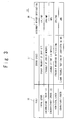
- Fig. 3 is a table showing the error table 35.
- the error causes 37 and the kinds 36 of the errors are related in the error table 35.
- the classification of the error causes into the respective kinds of the errors is set by considering the influence level on the system.
- the kinds 36 are a fatal error, an uncorrectable error [1], an uncorrectable error [2], a non-fatal error and a correctable error.
- An error cause 37 resulting in the fatal error indicates a heavy trouble of a chip set including the FT controllers (15, 25).
- the notification of the concrete error cause is omitted.
- an interrupt report destinations 38 are the CPUs (11, 21) and the BMCs (14, 24). OS (operating system) presets the interrupt report destinations 38 in the interrupt switching circuit 4.
- the error cause 37 resulting in the uncorrectable error [1] indicates the trouble in the CPU (11, 21) or memory (12, 22).
- the notification of the concrete error cause is omitted in the error table 35.
- the interrupt report destinations 38 are the CPUs (11, 21) and the BMCs (14, 24).
- the OS presets the interrupt report destinations 38 in the interrupt switching circuit 4.
- the error cause 37 resulting in the uncorrectable error [2] indicates the trouble in the I/O device 13.
- the notification of the concrete error cause is omitted in the error table 35.
- the interrupt report destinations 38 are the CPUs (11, 21).
- the OS presets the interrupt report destinations 38 in the interrupt switching circuit 4.
- the error cause 37 resulting in the non-fatal error mainly indicates the trouble with regard to the duplication.
- the notification of the concrete error cause is omitted in the error table 35.
- the OS presets the interrupt report destinations 38 in the interrupt switching circuit 4. However, the OS preliminarily sets one of the two CPUs (11, 21) for the CPU (active CPU) to be mainly operated, and sets the other for the CPU (standby CPU) to be auxiliarily operated. Then, in the case of the non-fatal error, the interrupt report destinations 38 are the CPU and BMC on the active CPU side or those on the standby CPU side.
- the error cause 37 resulting in the correctable error indicates the light trouble that can be corrected in the hardware module.
- the notification of the concrete error cause is omitted.
- the interrupt report destinations 38 are the BMCs (14, 24) .
- the OS presets the interrupt report destinations 38 in the interrupt switching circuit 4.
- the CPU module mode register 6 stores the setting that the OS preliminarily sets one of the two CPUs (11, 21) for the CPU (active CPU) to be mainly operated and sets the other for the CPU (standby CPU) to be auxiliarily operated.
- the error cause register 3 stores the error cause (37) and its kind (36) transmitted from the trouble detecting circuit 2. The portion where the error occurs and its cause are known from them. Then, the kind of the error is transmitted to the interrupt switching circuit 4.
- the BMC 14 directly reads the kind of the error from the error cause register 3.
- the CPU 11 reads the kind of the error from the error cause register 3 through the visible setting register 5.
- the interrupt switching circuit 4 sends the interrupt to at least one of the CPU 11, the CPU 21 and the BMC 14, in reference to the setting, based on the kind of the error outputted from the error cause register 3.
- Fig. 4 is a block diagram showing the configuration of the interrupt switching circuit 4.
- the interrupt switching circuit 4 includes a BMC interrupt report register 41, a CPU interrupt report register 46, an active/standby judging circuit 47, and an interrupt controller 48.
- the CPU interrupt report register 46 includes an active SMI interrupt report register 42, an active IRQ interrupt report register 43, a standby SMI interrupt report register 44 and a standby IRQ interrupt report register 45.
- the error cause register 3 includes A to E registers corresponding to the error causes of five kinds. That is, the error causes (37) corresponding to the error kinds (36) are inputted to the A to E registers. For example, if the kind of the error cause is the fatal error, the data indicating the error cause (37) is inputted to the A register, and "0" is inputted to all of the other registers. If the kind of the error cause is the uncorrectable error [1], the data indicating the error cause (37) is inputted to the B register, and "0" is inputted to all of the other registers. If the kind of the error cause is the uncorrectable error [2], the data indicating the error cause (37) is inputted to the C register, and "0" is inputted to all of the other registers.
- the error cause register 3 outputs the data of the A to E registers to the BMC interrupt report register 41.
- the BMC interrupt report register 41 includes L1 to L5 registers corresponding to the A to E registers included in the error cause register 3. That is, the data of the A register is inputted to the L1 register, the data of the B register is inputted to the L2 register, the data of the C register is inputted to the L3 register, the data of the D register is inputted to the L4 register, and the data of the E register is inputted to the L5 register.
- Fig. 4 indicated by a solid circle, and hereafter, similarly indicated
- the BMC interrupt report register 41 outputs the instruction to the interrupt controller 48.
- the interrupt controller 48 can report the interrupt to the BMC 14. Also, the BMC interrupt report register 41 outputs the data of the L1 to L5 registers to the active SMI interrupt report register 42 of the CPU interrupt report register 46.
- the active SMI interrupt report register 42 includes M1 to M5 registers corresponding to the L1 to L5 registers. That is, the data of the L1 register is inputted to the M1 register, the data of the L2 register is inputted to the M2 register, the data of the L3 register is inputted to the M3 register, the data of the L4 register is inputted to the M4 register, and the data of the L5 register is inputted to the M5 register.
- the active SMI interrupt report register 42 outputs the interrupt to the active/standby judging circuit 47.
- the active/standby judging circuit 47 can report a SMI (System Management Interrupt) to the active CPU through the interrupt controller 48. Also, the active SMI interrupt report register 42 outputs the data of the M1 to M5 registers to the active IRQ interrupt report register 43.
- SMI System Management Interrupt
- the Active IRQ interrupt report register 43 includes N1 to N5 registers corresponding to the M1 to M5 registers. That is, the data of the M1 register is inputted to the N1 register, the data of the M2 register is inputted to the N2 register, the data of the M3 register is inputted to the N3 register, the data of the M4 register is inputted to the N4 register, and the data of the M5 register is inputted to the N5 register.
- the active IRQ interrupt report register 43 outputs the interrupt to the active/standby judging circuit 47.
- the active/standby judging circuit 47 can report an IRQ (Interrupt ReQuest) to the active CPU through the interrupt controller 48. Also, the active IRQ interrupt report register 43 outputs the data of the N1 to N5 registers to the standby SMI interrupt report register 44.
- IRQ Interrupt ReQuest
- the standby SMI interrupt report register 44 includes O1 to O5 registers corresponding to the N1 to N5 registers. That is, the data of the N1 register is inputted to the O1 register, the data of the N2 register is inputted to the 02 register, the data of the N3 register is inputted to the 03 register, the data of the N4 register is inputted to the 04 register, and the data of the N5 register is inputted to the 05 register.
- the standby SMI interrupt report register 44 outputs the interrupt to the active/standby judging circuit 47.
- the active/standby judging circuit 47 can report the SMI to the standby CPU through the interrupt controller 48. Also, the standby SMI interrupt report register 44 outputs the data of the O1 to O5 registers to the standby IRQ interrupt report register 45.
- the standby IRQ interrupt report register 45 includes P1 to P5 registers corresponding to the O1 to O5 registers. That is, the data of the O1 register is inputted to the P1 register, the data of the 02 register is inputted to the P2 register, the data of the O3 register is inputted to the P3 register, the data of the 04 register is inputted to the P4 register, and the data of the 05 register is inputted to the P5 register.
- the standby IRQ interrupt report register 45 does not output the interrupt to the active/standby judging circuit 47.
- the active/standby judging circuit 47 does not report the IRQ to the standby CPU through the interrupt controller 48.
- Fig. 4 shows an example of the setting of the BMC interrupt report register 41 and the CPU interrupt report register 46.
- the report or non-report of the interrupt can be set at the desirable states.
- the active/standby judging circuit 47 on the CPU 21 side if receiving the interrupt from the standby SMI interrupt report register 44, outputs the SMI to the interrupt controller 48, and if receiving the standby IRQ interrupt report register 45, outputs the IRQ to the interrupt controller 48.
- the interrupt controller 48 if receiving the interrupt from the BMC interrupt report register 41, reports the interrupt to the BMC 14.
- the interrupt controller 48 if receiving the interrupt from the active/standby judging circuit 47, reports the interrupt of the SMI or IRQ to the CPU 11 or CPU 21,
- the visible setting register 5 masks the particular register(s) of the error cause register 3 such that the particular register(s) cannot be read, when the CPUs (11, 12) read the error cause register 3.
- Fig. 5 is a block diagram showing the visible setting register 5.
- the visible setting register 5 includes Q1 to Q5 registers.
- the CPU (11, 21) reads data from the A to E registers of the error cause register 3, an AND operation result of the A to E registers and the Q1 to Q5 registers is outputted to the CPU (11, 21).
- the data of the E register is masked and is not viewed from the CPUs (11, 21). That is, the CPU (11, 21) cannot recognize the interrupt of the correctable error.
- Fig. 5 shows an example of the setting of the visible setting register 5 is the example.
- the mask of the report of the interrupt can be set at a desirable state.
- Figs. 6, 8, 10, 12 and 14 are flowcharts showing the embodiment of the method for dealing with errors (the operation of the embodiment of the computer system) of the present invention.
- Figs. 7, 9, 11, 13 and 15 are schematic views showing the state of the computer system in the method for dealing with errors of the present invention.
- the OS sets each of the interrupt report registers in the duplicated use manner when the system is duplicated.
- the setting includes the settings shown in Figs. 2 to 4.
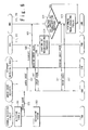
- FIG. 6 is the flowchart showing the method for dealing with errors in the case that the fatal error occurs.
- the trouble detecting circuit 2 detects the heavy trouble of the chip set including the FT controller (e.g. 25) (Step S01).
- the trouble detecting circuit 2 reports the error cause of the fatal error to the error cause register 3 (Step S02)
- the trouble detecting circuit 2 separates the system (e.g. the second system 20) on the side where the trouble occurs from the system under the operation (e.g. the first system 10) (Step S03) .
- Fig. 7 is a schematic view showing this state of the computer system.
- the error cause register 3 outputs the error cause and the kind of the error to the interrupt switching circuit 4 (Step S04).
- the interrupt switching circuit 4 outputs the interrupts (an SMI interrupt 51 and a BMC interrupt 52) to the CPU (e.g. 11) and the BMC (e.g. 14) based on the setting of Fig. 4 (Steps S05, S06) .
- the OS reads the error cause register 3 if it is operable (Steps S07, S08) .
- the OS carries out preset troubleshooting processes (e.g. a log collecting, a trouble recovering process) based on of the error cause (Step S09) .
- the self-memory e.g. the non-volatile memory 33 shown in Fig. 2, hereafter similarly
- Fig. 8 is the flowchart showing the method for dealing with errors in the case that the uncorrectable error [1] occurs.
- the trouble detecting circuit 2 detects the trouble of the CPU (e.g. 11) or the memory (e.g. 12) (Step S21). The trouble detecting circuit 2 reports the error cause of the uncorrectable error [1] to the error cause register 3 (Step S22). Also, the trouble detecting circuit 2 separates the CPU (e.g. 11) or the memory (e.g. 12) where the error occurs from the system, and continues the duplicated operation still in the other portions of the system (Step S23).
- Fig. 9 is a schematic view showing this state of the computer system. Here, Fig. 9 shows an example where the troubles occur in both of the CPU 11 and the memory 12.
- the error cause register 3 outputs the error cause and the kind of the error to the interrupt switching circuit 4 (Step S24).
- the interrupt switching circuit 4 outputs the interrupts (the SMI interrupt 51 and the BMC interrupt 52) to the CPU (e.g. 11) and the BMC (e.g. 14) based on the setting of Fig. 4 (Steps S25, S26).
- the OS reads the error cause register 3 if it is operable (Steps S27, S28).
- the OS carries out the preset troubleshooting processes (the log collecting, the trouble recovering process) based on the error cause (Step S29).
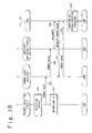
- Fig. 10 is the flowchart showing the method for dealing with errors in the case that the uncorrectable error [2] occurs.
- the trouble detecting circuit 2 detects the trouble of the I/O device (e.g. 13) (Step S41). The trouble detecting circuit 2 reports the error cause of the uncorrectable error [2] to the error cause register 3 (Step S42). Also, the trouble detecting circuit 2 separates the I/O device (e.g. 13) where the trouble occurs from the system, and continues the duplicated operation still in the other portions of the system (Step S43).
- Fig. 11 is a schematic view showing this state of the computer system.
- the error cause register 3 outputs the error cause and the kind of the error to the interrupt switching circuit 4 (Step S44).
- the interrupt switching circuit 4 outputs the interrupts (an SMI interrupt 53 and an SMI interrupt 54) to the CPU (e.g. 11) based on the setting of Fig. 4 (Step S45).
- the OS reads the error cause register 3 (Steps S46, S47).
- the OS carries out the preset troubleshooting processes (the log collecting, the trouble recovering process) based on the error cause (Step S48).
- Fig. 12 is the flowchart showing the method for dealing with errors in the case that the non-fatal error occurs.
- the OS sets the CPU 11 as the CPU (active CPU) to be mainly operated, and sets the CPU 21 as the CPU (standby CPU) to be auxiliarily operated.
- the OS sets the interrupt reported to the active CPU side as the normal interrupt (IRQ) and sets the interrupt reported to the standby CPU side as the SMI (system management interrupt).
- IRQ normal interrupt
- SMI system management interrupt
- the trouble detecting circuit 2 detects the mismatching between the operation of the first system 10 and the operation of the second system 20 (Step S61).
- the trouble detecting circuit 2 reports the error cause of the non-fatal error to the error cause register 3 (Step S62).
- the error cause register 3 outputs the error cause and the kind of the error to the interrupt switching circuit 4 (Step S63).
- the CPU interrupt report register 46 of the interrupt switching circuit 4 outputs the interrupts of the active IRQ interrupt report register 43 and the standby SMI interrupt report register 44 to the active/standby judging circuit 47, based on the setting shown in Fig. 4.
- the active/standby judging circuit 47 reports the interrupt of any one of the active IRQ interrupt report register 43 and the standby SMI interrupt report register 44 to the interrupt controller 48, based on the information preset for the CPU module mode register 6.
- the interrupt controller 48 reports an IRQ interrupt 55 on the active side to the CPU (e.g. 11) on the active side (Step S64) and reports an SMI interrupt 56 on the standby side to the CPU (e.g. 21) on the standby side (Step S65). In this way, the different interrupts can be reported to the CPU (e.g. 11) on the active side and the CPU (e.g. 21) on the standby side.
- the CPU (e.g. 21 the interrupt handler of OS) on the standby side, if receiving the SMI interrupt, reads the error cause register 3 (Steps S66, S67) and carries out the process necessary for the re-synchronization (step S68). Then, the CPU on the standby side waits for the instruction from the CPU (e.g. 11) on the active side.
- the CPU (e.g. 11 the interrupt handler of OS) on the active side, if receiving the IRQ interrupt, reads the error cause register 3 (Steps S69, S70) .
- Fig. 13 is a schematic view showing this state of the computer system. After that, the CPU on the standby side can execute the re-synchronization process (Step S73), and the duplicated operation is again started.
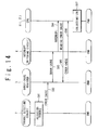
- Fig. 14 is the flowchart showing the method for dealing with errors in case that the correctable error occurs.
- the trouble detecting circuit 2 detects a predetermined light trouble (Step S81)
- the trouble detecting circuit 2 reports the error cause of the correctable error to the error cause register 3 (Step S82) .
- the error cause register 3 outputs the error cause and the kind of the error to the interrupt switching circuit 4 (Step S83).
- the interrupt switching circuit 4 outputs the interrupt (BMC interrupt 58) to the BMC (e.g. 14) based on the setting of Fig. 4 (Step S84).
- Fig. 15 is a schematic view showing this state of the computer system.
- the BMC when receiving the interrupt, reads the error cause register 3 (Steps S85, S86).
- the BMC e.g. 14
- the BMC performs only the log collecting on the self-memory based on the error cause (Step S87).
- the CPU does not receive the interrupt report.
- the CPU does not recognize that the error occurs and does not read the error cause register 3. Then, the CPU continues the operation.
- the OS reads the error cause register 3.
- the visible setting register 6 is installed.
- the OS preliminarily performs the mask setting for the correctable error on the visible setting register 6, as shown in Fig. 5. Consequently, if the error cause register 3 is read from the CPU (OS) side, the data where the error cause register 3 and the visible setting register 6 are AND-operated is returned to the OS. For this reason, the masked portion is not viewed from the OS. That is, for example, even if the different error simultaneously occurs and the OS reads the error cause register 3, the desynchronization does not occur.
- the computer system deals with the error.
- the destination of the interrupt report regarding an error can be changed based on the influence level on the system. Consequently, the system can deal with the error based on an influence level on the system.
Landscapes
- Engineering & Computer Science (AREA)
- Theoretical Computer Science (AREA)
- Quality & Reliability (AREA)
- Physics & Mathematics (AREA)
- General Engineering & Computer Science (AREA)
- General Physics & Mathematics (AREA)
- Hardware Redundancy (AREA)
Abstract
A computer system includes a plurality of systems (10, 20) configured to be connected to each other by links and to operate synchronously each other. Each of said plurality of systems (10, 20) includes a fault tolerant controller (15, 25), a CPU (11, 21), a baseboard management controller (14, 24) and a plurality of hardware modules (12/13, 22/23), The CPU (11, 21) is connected with the fault tolerant controller (15, 25). The baseboard management controller (15, 25) is connected with the fault tolerant controller (15, 25) . The plurality of hardware modules (12/13, 22/23) is connected with the fault tolerant controller (15, 25). When receiving a trouble which occurs in any of the plurality of systems (10, 20), the fault tolerant controller (15, 25) outputs an interrupt regarding the trouble to at least one of the CPU (11, 21) and the baseboard management controller (14, 24) predetermined correspondingly to the trouble.
Description
- The present invention relates to a computer system and a method for dealing with errors in a computer system, and more particularly relates to a method for dealing with errors used in a multiplexed computer system.
- It is known that there is a computer system having a high reliability such as a fault tolerant computer system. In the fault tolerant computer system, all of hardware modules constituting the system are duplicated or multiplexed. All of the hardware modules are synchronously operated. For this reason, for example, even if a certain portion of the system is troubled, the hardware module with the trouble can be separated, thereby continuing the process under the normal hardware modules. Thus, the tolerance for the trouble is improved.
- Errors occurring in the computer system have various levels of influences on the system. If the same method is used to deal with all the errors, the method for dealing with the errors having the high influence level must be used. In this case, the method unnecessarily thoroughly deals with the error, even though the error has the low influence level. This makes the burden on the system unnecessarily large, which leads to the possibility that the processing performance is excessively influenced. Thus, a technique is desired, which can deal with the error correspondingly to the influence level on the system.
- In conjunction with the above description, Japanese Laid-Open Patent Application (JP-A-Heisei, 7-200334) discloses a dually synchronous driving method. In this dually synchronous driving method, two processor groups, which are substantially equal to each other, are driven synchronously with each other by the same command and the same data input. One of the two processor groups is assigned to an active group, and the other is assigned to a standby group. A trouble detecting circuit for detecting a hardware trouble is connected to each of the two processor groups. Here, if the hardware trouble occurs in a processor group, an operation cannot be normally continued in the processor group. Each of the two processors contains a first controller and a second controller. The first controller belonging to the active group executes an interrupting process based on a detection output from the trouble detecting circuit of the active group, releases the synchronous state, and then stops displaying the active group. The second controller belonging to the standby group starts displaying the active group based on the detection output from the trouble detecting circuit of a partner's group, and then continues the operation at a single mode.
- It is therefore an object of the present invention to provide a computer system and a method for dealing with an error, which can change a destination of an interrupt report regarding an error in a multiplexed computer system based on an influence level on the system.
- Also, another object of the present invention is to provide a computer system and a method for dealing with an error, which can deal with an error based on an influence level on the system.
- This and other objects, features and advantages of the present invention will be readily ascertained by referring to the following description and drawings.
- In order to achieve an aspect of the present invention, the present invention provides a computer system including a plurality of systems configured to be connected to each other by links and to operate synchronously each other. Each of the plurality of systems includes: a fault tolerant controller; a CPU configured to be connected with the fault tolerant controller; a baseboard management controller configured to be connected with the fault tolerant controller; and a plurality of hardware modules configured to be connected with the fault tolerant controller. When receiving a trouble which occurs in any of the plurality of systems, the fault tolerant controller outputs an interrupt regarding the trouble to at least one of the CPU and the baseboard management controller predetermined correspondingly to the trouble.
- In the computer system, the fault tolerant controller may include: a trouble detecting circuit configured to judges a cause and a kind of the trouble; an error cause storage unit configured to store the cause and the kind, and an interrupt switching circuit configured to output the interrupt to the at least one of the CPU and the baseboard management controller predetermined correspondingly to the kind of the trouble.
- In the computer system, when the trouble occurs in the other system of the plurality of systems, the trouble detecting circuit may separate the other system in which the trouble occurs. The interrupt switching circuit may output the interrupt to the CPU and the baseboard management controller.
- In the computer system, when the trouble occurs in one of the CPU and a memory as one of the plurality of hardware modules, the trouble detecting circuit may separate the one of the CPU and the memory in which the trouble occurs. The interrupt switching circuit may output the interrupt to the CPU and the baseboard management controller.
- In the computer system, when the trouble occurs in an I/O device as one of the plurality of hardware modules, the trouble detecting circuit may separate the I/O device in which the trouble occurs. The interrupt switching circuit may output the interrupt to the CPU.
- In the computer system, the fault tolerant controller may further include a CPU module mode storage unit configured to store a CPU mode data indicating which of an active CPU and a standby CPU the CPU connected with the fault tolerant controller is. When the trouble is related to a multiplexing of the plurality of systems, the interrupt switching circuit may output the interrupt to the CPU which is connected with the interrupt switching circuit, based on the CPU mode data in the CPU module mode storage unit.
- In the computer system, when the trouble is light trouble that can be corrected by one of the plurality of hardware modules, the interrupt switching circuit may output the interrupt to the baseboard management controller.
- In the computer system, the at least one of the CPU and the baseboard management controller which receives the interrupt regarding the trouble may read the cause from the error cause storage unit and may carry out processes with regard to the trouble correspondingly to the cause.
- In the computer system, the fault tolerant controller may further include: a visible setting storage unit configured to mask the cause based on the kind when the CPU reads the cause from the error cause storage unit.
- In order to achieve another aspect of the present invention, the present invention provides a method for dealing with errors, including: (a) judging a cause and a kind of a trouble, when the trouble occurs in any of a plurality of systems included in a computer system, wherein the plurality of systems is connected to each other by links and operates synchronously each other; and (b) outputting an interrupt regarding the trouble to at least one destination predetermined correspondingly to the kind of the trouble.
- The method for dealing with errors may further include: (c) carrying out processes regarding the trouble correspondingly to the cause, by the at least one destination.
- In the method for dealing with errors, each of the plurality of systems may include: a fault tolerant controller; a CPU configured to be connected with the fault tolerant controller; a baseboard management controller configured to be connected with the fault tolerant controller; and a plurality of hardware modules configured to be connected with the fault tolerant controller. The step (b) may include: (b1) outputting the interrupt to at least one of the CPU and the baseboard management controller predetermined correspondingly to the kind of the trouble, by the fault tolerant controller.
- In the method for dealing with errors, the fault tolerant controller may include: a trouble detecting circuit; an error cause storage unit configured to be connected with the trouble detecting circuit, and an interrupt switching circuit configured to be connected with the error cause storage unit. The step (a) may include: (a1) judging the cause and the kind by the trouble detecting circuit, and (a2) storing the cause and the kind by the error cause storage unit. The step (b1) may include: (b11) outputting the interrupt to the at least one of the CPU and the baseboard management controller by the interrupt switching circuit.
- In the method for dealing with errors, when the trouble occurs in the other system of the plurality of systems, the step (b1) may further include: (b12) separating the other system in which the trouble occurs by the trouble detecting circuit, and (b13) outputting the interrupt to the CPU and the baseboard management controller by the interrupt switching circuit.
- In the method for dealing with errors, when the trouble occurs in one of the CPU and a memory as one of the plurality of hardware modules, the step (b1) may further include: (b14) separating the one of the CPU and the memory in which the trouble occurs by the trouble detecting circuit, and (b15) outputting the interrupt to the CPU and the baseboard management controller by the interrupt switching circuit.
- In the method for dealing with errors, when the trouble occurs in a I/O device as one of the plurality of hardware modules, the step (b1) may further include: (b16) separating the I/O device in which the trouble occurs by the trouble detecting circuit, and (b17) outputting the interrupt to the CPU by the interrupt switching circuit.
- In the method for dealing with errors, the fault tolerant controller may further include: a CPU module mode storage unit configured to store a CPU mode data indicating which of an active CPU and a standby CPU the CPU connected with the fault tolerant controller is. When the trouble is related to a multiplexing of the plurality of systems, the step (b1) may further include: (b18) circuit outputting the interrupt to the CPU which is connected with the interrupt switching circuit, based on the CPU mode data in the CPU module mode storage unit, by the interrupt switching.
- In the method for dealing with errors, when the trouble is light trouble which can be corrected by one of the plurality of hardware modules, the step (b1) may further include: (b19) outputting the interrupt to the baseboard management controller by the interrupt switching circuit.
- The method for dealing with errors may further include: (c) reading the cause from the error cause storage unit and carrying out processes with regard to the trouble correspondingly to the cause by the at least one of the CPU and the baseboard management controller which receives the interrupt.
- In the method for dealing with errors, the fault tolerant controller may further include: a visible setting storage unit. The step (c) may include: (c1) masking the cause based on the kind when the CPU reads the cause from the error cause storage unit by the visible setting storage unit.
-
- Fig. 1 is a block diagram showing the configuration of the embodiment of the computer system of the present invention;
- Fig. 2 is a block diagram showing the configuration of the first system in the present invention;
- Fig. 3 is a table showing the error table;
- Fig. 4 is a block diagram showing the configuration of the interrupt switching circuit;
- Fig. 5 is a block diagram showing the visible setting register;
- Fig. 6 is the flowchart showing the method for dealing with errors in the case that the fatal error occurs;
- Fig. 7 is a schematic view showing the state of the computer system in the method for dealing with the fatal error;
- Fig. 8 is the flowchart showing the method for dealing with errors in the case that the uncorrectable error [1] occurs;
- Fig. 9 is a schematic view showing the state of the computer system in the method for dealing with the uncorrectable error [1];
- Fig. 10 is the flowchart showing the method for dealing with errors in the case that the uncorrectable error [2] occurs;
- Fig. 11 is a schematic view showing the state of the computer system in the method for dealing with the uncorrectable error [2];
- Fig. 12 is the flowchart showing the method for dealing with errors in the case that the non-fatal error occurs;
- Fig. 13 is a schematic view showing the state of the computer system in the method for dealing with the non-fatal error;
- Fig. 14 is the flowchart showing the method for dealing with errors in case that the correctable error occurs; and
- Fig. 15 is a schematic view showing the state of the computer system in the method for dealing with the correctable error.
- Embodiments of a computer system and a method for dealing with errors in a computer system of the present invention will be described below with reference to the attached drawings.
- A configuration of the embodiment of the computer system of the present invention is explained. Fig. 1 is a block diagram showing the configuration of the embodiment of the computer system of the present invention. Here, a duplicated fault tolerant computer system is explained as an example of the computer system of the present invention.
- A fault
tolerant computer system 30 has afirst system 10 and asecond system 20. Thefirst system 10 and thesecond system 20 are synchronously operated and connected so as to be able to transmit/receive signals through alink 31. - The
first system 10 includes hardware modules, such as a fault tolerant controller (hereinafter, referred to as a FT controller) 15, a CPU (central processing unit) 11, amemory 12, an I/O device 13 and a baseboard management controller (hereafter, referred to as a BMC) 14. TheFT controller 15 is connected to each hardware module (theCPU 11, thememory 12, the I/O device 13 and the BMC 14) and carries out synchronous operation processes and a process for dealing with errors when an error occurs. The process for dealing with errors is exemplified by a control with regard to an interrupt and a control with regard to a switching. - Similarly, the
second system 20 includes hardware modules, such as aFT controller 25, aCPU 21, amemory 22, an I/O device 23 and aBMC 24. TheFT controller 25 is connected to each hardware module (theCPU 21, thememory 22, the I/O device 23 and the BMC 24) and carries out the synchronous operation processes and the process for dealing with errors when an error occurs. The process for dealing with errors is exemplified by a control with regard to an interrupt and a control with regard to a switching. - The
FT controller 15 and theFT controller 25 are connected through thelink 31 and carry out the synchronous operation processes and the process for dealing with errors when an error occurs. The process for dealing with errors is exemplified by a control with regard to an interrupt and a control with regard to a switching. - The configuration for executing the method (process) for dealing with errors of the present invention in the
FT controller 15 will be described below. Incidentally, since that of theFT controller 25 is also similar, its explanation is omitted. Fig. 2 is a block diagram showing the configuration of thefirst system 10 in the present invention. TheFT controller 15 includes aprocessing circuit 1 for detecting an error and carrying out a process with regard to the error. Theprocessing circuit 1 includes atrouble detecting circuit 2, anerror cause register 3, an interrupt switchingcircuit 4, avisible setting register 5 and a CPUmodule mode register 6. - The
trouble detecting circuit 2 receives the data with regard to the error from any of theCPU 11, thememory 12, the I/O device 13 and theFT controller 25 in the other system. Then, if detecting the error, thetrouble detecting circuit 2 judges the error cause of the detected error and the kind of the error cause. Then, thetrouble detecting circuit 2 reports the detected error cause and its kind to theerror cause register 3. At this time, thetrouble detecting circuit 2 refers to an error table 35 to judge the kind of the detected error. The error table 35 includes the relation between error causes and kinds of errors. The detected error cause may be simultaneously transmitted to the interrupt switchingcircuit 4. - Further, based on the error cause, the
trouble detecting circuit 2 separates thesecond system 20 if the error occurs in thesecond system 20, or separates the hardware module (for example, theCPU 11, thememory 12 or the I/O device 13) if the error occurs in the hardware, from thefirst system 10 under the operation. When the hardware module having the error is separated, the operations except that of the separated module are continued still in the duplicated state. - Here, the error table 35 is explained. Fig. 3 is a table showing the error table 35. The error causes 37 and the
kinds 36 of the errors are related in the error table 35. The classification of the error causes into the respective kinds of the errors is set by considering the influence level on the system. - Five
kinds 36 of the errors are defined based on the influence level on the system. Thekinds 36 are a fatal error, an uncorrectable error [1], an uncorrectable error [2], a non-fatal error and a correctable error. - An
error cause 37 resulting in the fatal error indicates a heavy trouble of a chip set including the FT controllers (15, 25). In the error table 35, the notification of the concrete error cause is omitted. In the case of the fatal error, an interruptreport destinations 38 are the CPUs (11, 21) and the BMCs (14, 24). OS (operating system) presets the interruptreport destinations 38 in the interrupt switchingcircuit 4. - The
error cause 37 resulting in the uncorrectable error [1] indicates the trouble in the CPU (11, 21) or memory (12, 22). The notification of the concrete error cause is omitted in the error table 35. In the case of the uncorrectable error [1], the interruptreport destinations 38 are the CPUs (11, 21) and the BMCs (14, 24). The OS presets the interruptreport destinations 38 in the interrupt switchingcircuit 4. - The
error cause 37 resulting in the uncorrectable error [2] indicates the trouble in the I/O device 13. The notification of the concrete error cause is omitted in the error table 35. In the case of the uncorrectable error [2], the interruptreport destinations 38 are the CPUs (11, 21). The OS presets the interruptreport destinations 38 in the interrupt switchingcircuit 4. - The
error cause 37 resulting in the non-fatal error mainly indicates the trouble with regard to the duplication. The notification of the concrete error cause is omitted in the error table 35. The OS presets the interruptreport destinations 38 in the interrupt switchingcircuit 4. However, the OS preliminarily sets one of the two CPUs (11, 21) for the CPU (active CPU) to be mainly operated, and sets the other for the CPU (standby CPU) to be auxiliarily operated. Then, in the case of the non-fatal error, the interruptreport destinations 38 are the CPU and BMC on the active CPU side or those on the standby CPU side. - The
error cause 37 resulting in the correctable error indicates the light trouble that can be corrected in the hardware module. The notification of the concrete error cause is omitted. In the case of the correctable error, the interruptreport destinations 38 are the BMCs (14, 24) . The OS presets the interruptreport destinations 38 in the interrupt switchingcircuit 4. - With reference to Fig. 2, the CPU
module mode register 6 stores the setting that the OS preliminarily sets one of the two CPUs (11, 21) for the CPU (active CPU) to be mainly operated and sets the other for the CPU (standby CPU) to be auxiliarily operated. - The
error cause register 3 stores the error cause (37) and its kind (36) transmitted from thetrouble detecting circuit 2. The portion where the error occurs and its cause are known from them. Then, the kind of the error is transmitted to the interrupt switchingcircuit 4. TheBMC 14 directly reads the kind of the error from theerror cause register 3. TheCPU 11 reads the kind of the error from theerror cause register 3 through thevisible setting register 5. - The interrupt switching
circuit 4 sends the interrupt to at least one of theCPU 11, theCPU 21 and theBMC 14, in reference to the setting, based on the kind of the error outputted from theerror cause register 3. - Here, the interrupt switching
circuit 4 is further explained. Fig. 4 is a block diagram showing the configuration of the interrupt switchingcircuit 4. The interrupt switchingcircuit 4 includes a BMC interrupt report register 41, a CPU interrupt report register 46, an active/standby judging circuit 47, and an interruptcontroller 48. The CPU interrupt report register 46 includes an active SMI interrupt report register 42, an active IRQ interrupt report register 43, a standby SMI interrupt report register 44 and a standby IRQ interrupt report register 45. - The
error cause register 3 includes A to E registers corresponding to the error causes of five kinds. That is, the error causes (37) corresponding to the error kinds (36) are inputted to the A to E registers. For example, if the kind of the error cause is the fatal error, the data indicating the error cause (37) is inputted to the A register, and "0" is inputted to all of the other registers. If the kind of the error cause is the uncorrectable error [1], the data indicating the error cause (37) is inputted to the B register, and "0" is inputted to all of the other registers. If the kind of the error cause is the uncorrectable error [2], the data indicating the error cause (37) is inputted to the C register, and "0" is inputted to all of the other registers. If the kind of the error cause is the non-fatal error, the data indicating the error cause (37) is inputted to the D register, and "0" is inputted to all of the other registers. If the kind of the error cause is the correctable error, the data indicating the error cause (37) is inputted to the E register, and "0" is inputted to all of the other registers. Theerror cause register 3 outputs the data of the A to E registers to the BMC interrupt report register 41. - The BMC interrupt report register 41 includes L1 to L5 registers corresponding to the A to E registers included in the
error cause register 3. That is, the data of the A register is inputted to the L1 register, the data of the B register is inputted to the L2 register, the data of the C register is inputted to the L3 register, the data of the D register is inputted to the L4 register, and the data of the E register is inputted to the L5 register. In the setting of Fig. 4 (indicated by a solid circle, and hereafter, similarly indicated), if "1" is inputted to any of the L1 register, the L2 register and the L5 register among them, the BMC interrupt report register 41 outputs the instruction to the interruptcontroller 48. Thus, if the kind of the error cause is any of the fatal error, the uncorrectable error [1] and the correctable error, the interruptcontroller 48 can report the interrupt to theBMC 14. Also, the BMC interrupt report register 41 outputs the data of the L1 to L5 registers to the active SMI interrupt report register 42 of the CPU interrupt report register 46. - The active SMI interrupt report register 42 includes M1 to M5 registers corresponding to the L1 to L5 registers. That is, the data of the L1 register is inputted to the M1 register, the data of the L2 register is inputted to the M2 register, the data of the L3 register is inputted to the M3 register, the data of the L4 register is inputted to the M4 register, and the data of the L5 register is inputted to the M5 register. In the setting of Fig. 4, if "1" is inputted to any of the M1 register, the M2 register and the M3 register among them, the active SMI interrupt report register 42 outputs the interrupt to the active/
standby judging circuit 47. Thus, if the kind of the error cause is the fatal error, the uncorrectable error [1] and the uncorrectable error [2], the active/standby judging circuit 47 can report a SMI (System Management Interrupt) to the active CPU through the interruptcontroller 48. Also, the active SMI interrupt report register 42 outputs the data of the M1 to M5 registers to the active IRQ interrupt report register 43. - The Active IRQ interrupt report register 43 includes N1 to N5 registers corresponding to the M1 to M5 registers. That is, the data of the M1 register is inputted to the N1 register, the data of the M2 register is inputted to the N2 register, the data of the M3 register is inputted to the N3 register, the data of the M4 register is inputted to the N4 register, and the data of the M5 register is inputted to the N5 register. In the setting of Fig. 4, if "1" is inputted to the M4 register among them, the active IRQ interrupt report register 43 outputs the interrupt to the active/
standby judging circuit 47. Thus, if the kind of the error cause is the non-fatal error, the active/standby judging circuit 47 can report an IRQ (Interrupt ReQuest) to the active CPU through the interruptcontroller 48. Also, the active IRQ interrupt report register 43 outputs the data of the N1 to N5 registers to the standby SMI interrupt report register 44. - The standby SMI interrupt report register 44 includes O1 to O5 registers corresponding to the N1 to N5 registers. That is, the data of the N1 register is inputted to the O1 register, the data of the N2 register is inputted to the 02 register, the data of the N3 register is inputted to the 03 register, the data of the N4 register is inputted to the 04 register, and the data of the N5 register is inputted to the 05 register. In the setting of Fig. 4, if "1" is inputted to the O1 register, the O2 register, the O3 register and the O4 register among them, the standby SMI interrupt report register 44 outputs the interrupt to the active/
standby judging circuit 47. Thus, if the kind of the error cause is any of the fatal error, the uncorrectable error [1], the uncorrectable error [2] and the non-fatal error, the active/standby judging circuit 47 can report the SMI to the standby CPU through the interruptcontroller 48. Also, the standby SMI interrupt report register 44 outputs the data of the O1 to O5 registers to the standby IRQ interrupt report register 45. - The standby IRQ interrupt report register 45 includes P1 to P5 registers corresponding to the O1 to O5 registers. That is, the data of the O1 register is inputted to the P1 register, the data of the 02 register is inputted to the P2 register, the data of the O3 register is inputted to the P3 register, the data of the 04 register is inputted to the P4 register, and the data of the 05 register is inputted to the P5 register. In the setting of Fig. 4, even if "1" is inputted to any of the registers, the standby IRQ interrupt report register 45 does not output the interrupt to the active/
standby judging circuit 47. Thus, irrespective of the kind of the error cause, the active/standby judging circuit 47 does not report the IRQ to the standby CPU through the interruptcontroller 48. - Here, Fig. 4 shows an example of the setting of the BMC interrupt report register 41 and the CPU interrupt report register 46. The report or non-report of the interrupt can be set at the desirable states.
- The active/
standby judging circuit 47 determines whether or not the interrupt (SMI, IRQ) from the CPU interrupt report register 46 is outputted to the interruptcontroller 48, based on the data of the active CPU =CPU 11, the standby CPU =CPU 21 stored in the CPUmodule mode register 6. That is, the active/standby judging circuit 47 on theCPU 11 side, if receiving the interrupt from the active SMI interrupt report register 42, outputs the SMI to the interruptcontroller 48, and if receiving the interrupt from the active IRQ interrupt report register 43, outputs the IRQ to the interruptcontroller 48. The active/standby judging circuit 47 on theCPU 21 side, if receiving the interrupt from the standby SMI interrupt report register 44, outputs the SMI to the interruptcontroller 48, and if receiving the standby IRQ interrupt report register 45, outputs the IRQ to the interruptcontroller 48. - The interrupt
controller 48, if receiving the interrupt from the BMC interrupt report register 41, reports the interrupt to theBMC 14. The interruptcontroller 48, if receiving the interrupt from the active/standby judging circuit 47, reports the interrupt of the SMI or IRQ to theCPU 11 orCPU 21, - With reference to Fig. 2, the
visible setting register 5 masks the particular register(s) of theerror cause register 3 such that the particular register(s) cannot be read, when the CPUs (11, 12) read theerror cause register 3. - Here, the
visible setting register 5 is further explained. Fig. 5 is a block diagram showing thevisible setting register 5. Thevisible setting register 5 includes Q1 to Q5 registers. When the CPU (11, 21) reads data from the A to E registers of theerror cause register 3, an AND operation result of the A to E registers and the Q1 to Q5 registers is outputted to the CPU (11, 21). Thus, in the case of the setting of Fig. 5, the data of the E register is masked and is not viewed from the CPUs (11, 21). That is, the CPU (11, 21) cannot recognize the interrupt of the correctable error. - Here, Fig. 5 shows an example of the setting of the
visible setting register 5 is the example. The mask of the report of the interrupt can be set at a desirable state. - The embodiment of the method for dealing with errors (the operation of the embodiment of the computer system) of the present invention will be described below with reference to the attached drawings. Figs. 6, 8, 10, 12 and 14 are flowcharts showing the embodiment of the method for dealing with errors (the operation of the embodiment of the computer system) of the present invention. Figs. 7, 9, 11, 13 and 15 are schematic views showing the state of the computer system in the method for dealing with errors of the present invention.
- At first, the OS sets each of the interrupt report registers in the duplicated use manner when the system is duplicated. The setting includes the settings shown in Figs. 2 to 4.
- The case that the fatal error occurs will be described below. Fig. 6 is the flowchart showing the method for dealing with errors in the case that the fatal error occurs.
- The
trouble detecting circuit 2 detects the heavy trouble of the chip set including the FT controller (e.g. 25) (Step S01). Thetrouble detecting circuit 2 reports the error cause of the fatal error to the error cause register 3 (Step S02) Also, thetrouble detecting circuit 2 separates the system (e.g. the second system 20) on the side where the trouble occurs from the system under the operation (e.g. the first system 10) (Step S03) . Fig. 7 is a schematic view showing this state of the computer system. - Next, the
error cause register 3 outputs the error cause and the kind of the error to the interrupt switching circuit 4 (Step S04). The interrupt switchingcircuit 4 outputs the interrupts (an SMI interrupt 51 and a BMC interrupt 52) to the CPU (e.g. 11) and the BMC (e.g. 14) based on the setting of Fig. 4 (Steps S05, S06) . When the CPU (e.g. 11 = an interrupt handler of OS) receives the interrupt, the OS reads theerror cause register 3 if it is operable (Steps S07, S08) . The OS carries out preset troubleshooting processes (e.g. a log collecting, a trouble recovering process) based on of the error cause (Step S09) . - The BMC (e.g. 14) monitors whether or not the CPU (e.g. 11=OS) is operated (Step S10). Then, if the OS is not operated (Step S10: NO), the BMC (e.g. 14) reads the error cause register 3 (Steps S11, S12). Then, the BMC (e.g. 14) performs only the log collecting on the self-memory (e.g. the
non-volatile memory 33 shown in Fig. 2, hereafter similarly) based on the error cause, as the troubleshooting process (Step S13). - As mentioned above, in the case that the fatal error occurs, the computer system deals with the error.
- The case that the uncorrectable error [1] occurs will be described below. Fig. 8 is the flowchart showing the method for dealing with errors in the case that the uncorrectable error [1] occurs.
- The
trouble detecting circuit 2 detects the trouble of the CPU (e.g. 11) or the memory (e.g. 12) (Step S21). Thetrouble detecting circuit 2 reports the error cause of the uncorrectable error [1] to the error cause register 3 (Step S22). Also, thetrouble detecting circuit 2 separates the CPU (e.g. 11) or the memory (e.g. 12) where the error occurs from the system, and continues the duplicated operation still in the other portions of the system (Step S23). Fig. 9 is a schematic view showing this state of the computer system. Here, Fig. 9 shows an example where the troubles occur in both of theCPU 11 and thememory 12. - Next, the
error cause register 3 outputs the error cause and the kind of the error to the interrupt switching circuit 4 (Step S24). The interrupt switchingcircuit 4 outputs the interrupts (the SMI interrupt 51 and the BMC interrupt 52) to the CPU (e.g. 11) and the BMC (e.g. 14) based on the setting of Fig. 4 (Steps S25, S26). When the CPU (= the interrupt handler of OS) receives the interrupt, the OS reads theerror cause register 3 if it is operable (Steps S27, S28). The OS carries out the preset troubleshooting processes (the log collecting, the trouble recovering process) based on the error cause (Step S29). - The BMC (e.g. 14) monitors whether or not the CPU (e.g. 11=OS) is operated (Step S30). Then, if the OS is not operated (Step S30: NO), the BMC (e.g. 14) reads the error cause register 3 (Steps S31, S32). Then, the BMC (e.g. 14) performs only the log collecting on the self-memory based on the error cause, as the troubleshooting processes (Step S33).
- As mentioned above, in the case that the uncorrectable error [1] occurs, the computer system deals with the error.
- The case that the uncorrectable error [2] occurs will be described below. Fig. 10 is the flowchart showing the method for dealing with errors in the case that the uncorrectable error [2] occurs.
- The
trouble detecting circuit 2 detects the trouble of the I/O device (e.g. 13) (Step S41). Thetrouble detecting circuit 2 reports the error cause of the uncorrectable error [2] to the error cause register 3 (Step S42). Also, thetrouble detecting circuit 2 separates the I/O device (e.g. 13) where the trouble occurs from the system, and continues the duplicated operation still in the other portions of the system (Step S43). Fig. 11 is a schematic view showing this state of the computer system. - Next, the
error cause register 3 outputs the error cause and the kind of the error to the interrupt switching circuit 4 (Step S44). The interrupt switchingcircuit 4 outputs the interrupts (an SMI interrupt 53 and an SMI interrupt 54) to the CPU (e.g. 11) based on the setting of Fig. 4 (Step S45). When the CPU (= the interrupt handler of OS) receives the interrupt, the OS reads the error cause register 3 (Steps S46, S47). The OS carries out the preset troubleshooting processes (the log collecting, the trouble recovering process) based on the error cause (Step S48). - As mentioned above, in the case that the uncorrectable error [2] occurs, the computer system deals with the error.
- The case that the non-fatal error occurs will be described below. Fig. 12 is the flowchart showing the method for dealing with errors in the case that the non-fatal error occurs.
- Here, let us suppose that the OS sets the
CPU 11 as the CPU (active CPU) to be mainly operated, and sets theCPU 21 as the CPU (standby CPU) to be auxiliarily operated. Similarly, let us suppose that the OS sets the interrupt reported to the active CPU side as the normal interrupt (IRQ) and sets the interrupt reported to the standby CPU side as the SMI (system management interrupt). - The
trouble detecting circuit 2 detects the mismatching between the operation of thefirst system 10 and the operation of the second system 20 (Step S61). Thetrouble detecting circuit 2 reports the error cause of the non-fatal error to the error cause register 3 (Step S62). Theerror cause register 3 outputs the error cause and the kind of the error to the interrupt switching circuit 4 (Step S63). - The CPU interrupt report register 46 of the interrupt switching
circuit 4 outputs the interrupts of the active IRQ interrupt report register 43 and the standby SMI interrupt report register 44 to the active/standby judging circuit 47, based on the setting shown in Fig. 4. The active/standby judging circuit 47 reports the interrupt of any one of the active IRQ interrupt report register 43 and the standby SMI interrupt report register 44 to the interruptcontroller 48, based on the information preset for the CPUmodule mode register 6. The interruptcontroller 48 reports an IRQ interrupt 55 on the active side to the CPU (e.g. 11) on the active side (Step S64) and reports an SMI interrupt 56 on the standby side to the CPU (e.g. 21) on the standby side (Step S65). In this way, the different interrupts can be reported to the CPU (e.g. 11) on the active side and the CPU (e.g. 21) on the standby side. - The CPU (e.g. 21 = the interrupt handler of OS) on the standby side, if receiving the SMI interrupt, reads the error cause register 3 (Steps S66, S67) and carries out the process necessary for the re-synchronization (step S68). Then, the CPU on the standby side waits for the instruction from the CPU (e.g. 11) on the active side. The CPU (e.g. 11 = the interrupt handler of OS) on the active side, if receiving the IRQ interrupt, reads the error cause register 3 (Steps S69, S70) . Then, the CPU on the active side reads the setting necessary for the re-synchronization to the standby side CPU (Step S71) and carries out its copy process 57 (Step S72). Fig. 13 is a schematic view showing this state of the computer system. After that, the CPU on the standby side can execute the re-synchronization process (Step S73), and the duplicated operation is again started.
- As mentioned above, in the case that the non-fatal error occurs, the computer system deals with the error.
- The case that the correctable error occurs will be described below. Fig. 14 is the flowchart showing the method for dealing with errors in case that the correctable error occurs.
- The
trouble detecting circuit 2 detects a predetermined light trouble (Step S81) Thetrouble detecting circuit 2 reports the error cause of the correctable error to the error cause register 3 (Step S82) . Theerror cause register 3 outputs the error cause and the kind of the error to the interrupt switching circuit 4 (Step S83). The interrupt switchingcircuit 4 outputs the interrupt (BMC interrupt 58) to the BMC (e.g. 14) based on the setting of Fig. 4 (Step S84). Fig. 15 is a schematic view showing this state of the computer system. - The BMC (e.g. 14), when receiving the interrupt, reads the error cause register 3 (Steps S85, S86). The BMC (e.g. 14) performs only the log collecting on the self-memory based on the error cause (Step S87). At this time, the CPU (e.g. 14=OS) does not receive the interrupt report. Thus, the CPU does not recognize that the error occurs and does not read the
error cause register 3. Then, the CPU continues the operation. - Here, at that time, for example, if a different error simultaneously occurs, the OS reads the
error cause register 3. In this case, if there is not avisible setting register 6, a difference is generated in theerror cause register 3, between thefirst system 10 and thesecond system 20, and the desynchronization occurs. For this reason, in the present invention, thevisible setting register 6 is installed. Then, the OS preliminarily performs the mask setting for the correctable error on thevisible setting register 6, as shown in Fig. 5. Consequently, if theerror cause register 3 is read from the CPU (OS) side, the data where theerror cause register 3 and thevisible setting register 6 are AND-operated is returned to the OS. For this reason, the masked portion is not viewed from the OS. That is, for example, even if the different error simultaneously occurs and the OS reads theerror cause register 3, the desynchronization does not occur. - As mentioned above, in the case that the correctable error occurs, the computer system deals with the error.
- In this way, the present invention, by installing the register that can select the plurality of interrupts, the generated interrupt can be changed and the device for executing the process and the content of the process can be changed through the process for dealing with errors. Also, since the mask register is installed such that the error cause is not viewed from the CPU side, without any fact that the CPU (= OS) recognizes the error occurring, the process for dealing with errors can be executed only in the BMC.
- According to the present invention, with regard to the error in the multiplexed computer system, the destination of the interrupt report regarding an error can be changed based on the influence level on the system. Consequently, the system can deal with the error based on an influence level on the system.
- It is apparent that the present invention is not limited to the above embodiment, that may be modified and changed without departing form the scope and spirit of the invention.
Claims (20)
- A computer system comprising:a plurality of systems (10, 20) configured to be connected to each other by links and to operate synchronously each other,wherein each of said plurality of systems (10, 20) comprises:a fault tolerant controller (15, 25),a CPU (11, 21) configured to be connected with said fault tolerant controller (15, 25),a baseboard management controller (14, 24) configured to be connected with said fault tolerant controller (15, 25), anda plurality of hardware modules (12/13, 22/23) configured to be connected with said fault tolerant controller (15, 25),when receiving a trouble which occurs in any of said plurality of systems (10, 20), said fault tolerant controller (15, 25) outputs an interrupt regarding said trouble to at least one of said CPU (11, 21) and said baseboard management controller (14, 24) predetermined correspondingly to said trouble.
- The computer system according to claim 1, wherein said fault tolerant controller (15, 25) comprises:a trouble detecting circuit (2) configured to judges a cause and a kind of said trouble,an error cause storage unit (3) configured to store said cause and said kind, andan interrupt switching circuit (4) configured to output said interrupt to said at least one of said CPU (11, 21) and said baseboard management controller (14, 24) predetermined correspondingly to said kind of said trouble.
- The computer system according to claim 2, wherein when said trouble occurs in the other system of said plurality of systems (10, 20),
said trouble detecting circuit (2) separates said other system in which said trouble occurs, and
said interrupt switching circuit (4) outputs said interrupt to said CPU (11, 21) and said baseboard management controller (14, 24). - The computer system according to claim 2, wherein when said trouble occurs in one of said CPU (11, 21) and a memory (12, 22) as one of said plurality of hardware modules (12/13, 22/23),
said trouble detecting circuit (2) separates said one of said CPU (11, 21) and said memory (12, 22) in which said trouble occurs, and
said interrupt switching circuit (4) outputs said interrupt to said CPU (11, 21) and said baseboard management controller (14, 24). - The computer system according to claim 2, wherein when said trouble occurs in a I/O device as one of said plurality of hardware modules (12/13, 22/23),
said trouble detecting circuit (2) separates said I/O device in which said trouble occurs, and
said interrupt switching circuit (4) outputs said interrupt to said CPU (11, 21). - The computer system according to claim 2, wherein said fault tolerant controller (15, 25) further comprises:a CPU module mode storage unit (6) configured to store a CPU mode data indicating which of an active CPU and a standby CPU said CPU (11, 21) connected with said fault tolerant controller (15, 25) is,when said trouble is related to a multiplexing of said plurality of systems (10, 20),said interrupt switching circuit (4) outputs said interrupt to said CPU (11, 21) which is connected with said interrupt switching circuit (4), based on said CPU mode data in said CPU module mode storage unit (6).
- The computer system according to claim 2, wherein when said trouble is light trouble which can be corrected by one of said plurality of hardware modules (12/13, 22/23),
said interrupt switching circuit (4) outputs said interrupt to said baseboard management controller (14, 24). - The computer system according to any one of claims 2 to 7, wherein said at least one of said CPU (11, 21) and said baseboard management controller (14, 24) which receives said interrupt regarding said trouble reads said cause from said error cause storage unit (3) and carries out processes with regard to said trouble correspondingly to said cause.
- The computer system according to claim 8, wherein said fault tolerant controller (15, 25) further comprises:a visible setting storage unit configured to mask said cause based on said kind when said CPU (11, 21) reads said cause from said error cause storage unit (3).
- A method for dealing with errors, comprising:(a) judging a cause and a kind of a trouble, when said trouble occurs in any of a plurality of systems (10, 20) included in a computer system, wherein said plurality of systems (10, 20) is connected to each other by links and operates synchronously each other; and(b) outputting an interrupt regarding said trouble to at least one destination predetermined correspondingly to said kind of said trouble.
- The method for dealing with errors according to claim 10, further comprising:(c) carrying out processes regarding said trouble correspondingly to said cause, by said at least one destination.
- The method for dealing with errors according to claim 10, wherein each of said plurality of systems (10, 20) comprises:a fault tolerant controller (15, 25),a CPU (11, 21) configured to be connected with said fault tolerant controller (15, 25),a baseboard management controller (14, 24) configured to be connected with said fault tolerant controller (15, 25), anda plurality of hardware modules (12/13, 22/23) configured to be connected with said fault tolerant controller (15, 25),said step (b) comprises:(b1) outputting said interrupt to at least one of said CPU (11, 21) and said baseboard management controller (14, 24) predetermined correspondingly to said kind of said trouble, by said fault tolerant controller (15, 25).
- The method for dealing with errors according to claim 12, wherein said fault tolerant controller (15, 25) comprises:a trouble detecting circuit (2),an error cause storage unit (3) configured to be connected with said trouble detecting circuit (2), andan interrupt switching circuit (4) configured to be connected with said error cause storage unit (3),said step (a) comprises:(a1) judging said cause and said kind by said trouble detecting circuit (2), and(a2) storing said cause and said kind by said error cause storage unit (3),said step (b1) comprises:(b11) outputting said interrupt to said at least one of said CPU (11, 21) and said baseboard management controller (14, 24) by said interrupt switching circuit (4).
- The method for dealing with errors according to claim 13, wherein when said trouble occurs in the other system of said plurality of systems (10, 20),
said step (b1) further comprises:(b12) separating said other system in which said trouble occurs by said trouble detecting circuit (2), and(b13) outputting said interrupt to said CPU (11, 21) and said baseboard management controller (14, 24) by said interrupt switching circuit (4). - The method for dealing with errors according to claim 13, wherein when said trouble occurs in one of said CPU (11, 21) and a memory (12, 22) as one of said plurality of hardware modules (12/13, 22/23),
said step (b1) further comprises:(b14) separating said one of said CPU (11, 21) and said memory (12, 22) in which said trouble occurs by said trouble detecting circuit (2), and(b15) outputting said interrupt to said CPU (11, 21) and said baseboard management controller (14, 24) by said interrupt switching circuit (4). - The method for dealing with errors according to claim 13, wherein when said trouble occurs in a I/O device as one of said plurality of hardware modules (12/13, 22/23),
said step (b1) further comprises:(b16) separating said I/O device in which said trouble occurs by said trouble detecting circuit (2), and(b17) outputting said interrupt to said CPU (11, 21) by said interrupt switching circuit (4). - The method for dealing with errors according to claim 13, wherein said fault tolerant controller (15, 25) further comprises:a CPU module mode storage unit (6) configured to store a CPU mode data indicating which of an active CPU and a standby CPU said CPU (11, 21) connected with said fault tolerant controller (15, 25) is,when said trouble is related to a multiplexing of said plurality of systems (10, 20),said step (b1) further comprises:(b18) circuit outputting said interrupt to said CPU (11, 21) which is connected with said interrupt switching circuit (4), based on said CPU mode data in said CPU module mode storage unit (6), by said interrupt switching.
- The method for dealing with errors according to claim 13, wherein when said trouble is light trouble which can be corrected by one of said plurality of hardware modules (12/13, 22/23),
said step (b1) further comprises:(b19) outputting said interrupt to said baseboard management controller (14, 24) by said interrupt switching circuit (4). - The method for dealing with errors according to any one of claims 13 to 18, further comprising:(c) reading said cause from said error cause storage unit (3) and carrying out processes with regard to said trouble correspondingly to said cause by said at least one of said CPU (11, 21) and said baseboard management controller (14, 24) which receives said interrupt.
- The method for dealing with errors according to claim 19, wherein said fault tolerant controller (15, 25) further comprises:a visible setting storage unit,said step (c) comprises:(c1) masking said cause based on said kind when said CPU (11, 21) reads said cause from said error cause storage unit (3) by said visible setting storage unit.
Applications Claiming Priority (1)
| Application Number | Priority Date | Filing Date | Title |
|---|---|---|---|
| JP2004368674A JP2006178557A (en) | 2004-12-21 | 2004-12-21 | Computer system and error handling method |
Publications (1)
| Publication Number | Publication Date |
|---|---|
| EP1674996A2 true EP1674996A2 (en) | 2006-06-28 |
Family
ID=36084300
Family Applications (1)
| Application Number | Title | Priority Date | Filing Date |
|---|---|---|---|
| EP05112568A Withdrawn EP1674996A2 (en) | 2004-12-21 | 2005-12-21 | Computer system and method for dealing with errors |
Country Status (6)
| Country | Link |
|---|---|
| US (1) | US7552359B2 (en) |
| EP (1) | EP1674996A2 (en) |
| JP (1) | JP2006178557A (en) |
| CN (1) | CN1794187A (en) |
| AU (1) | AU2005246993A1 (en) |
| CA (1) | CA2530893A1 (en) |
Families Citing this family (30)
| Publication number | Priority date | Publication date | Assignee | Title |
|---|---|---|---|---|
| US20070088988A1 (en) * | 2005-10-14 | 2007-04-19 | Dell Products L.P. | System and method for logging recoverable errors |
| KR100764062B1 (en) | 2006-05-01 | 2007-10-09 | 엘아이지넥스원 주식회사 | Aircraft Multiplexed Computer System |
| US7594144B2 (en) * | 2006-08-14 | 2009-09-22 | International Business Machines Corporation | Handling fatal computer hardware errors |
| JP4369467B2 (en) * | 2006-12-12 | 2009-11-18 | 富士通株式会社 | Data relay apparatus, storage apparatus, and data relay method |
| US7596648B2 (en) * | 2007-03-08 | 2009-09-29 | Dell Products L.P. | System and method for information handling system error recovery |
| US20080270827A1 (en) * | 2007-04-26 | 2008-10-30 | International Business Machines Corporation | Recovering diagnostic data after out-of-band data capture failure |
| US8448024B2 (en) * | 2007-05-16 | 2013-05-21 | Intel Corporation | Firmware assisted error handling scheme |
| JP2010033506A (en) * | 2008-07-31 | 2010-02-12 | Nec Corp | Duplication system, and active system determination method in duplication system |
| US8000052B2 (en) * | 2008-08-11 | 2011-08-16 | International Business Machines Corporation | Cartridge refresh and verify |
| US8458499B2 (en) * | 2009-08-07 | 2013-06-04 | International Business Machines Corporation | Method for reducing power state in a computer system out-of-band when a request for reducing the power state is not immediately serviceable in band according to a priority of the request |
| US8539285B2 (en) | 2010-06-22 | 2013-09-17 | International Business Machines Corporation | Systems for agile error determination and reporting and methods thereof |
| CN102467440A (en) * | 2010-11-09 | 2012-05-23 | 鸿富锦精密工业(深圳)有限公司 | Internal memory error detection system and method |
| CN102750194A (en) * | 2012-06-25 | 2012-10-24 | 浪潮电子信息产业股份有限公司 | Large-scale integrated circuit level error recording and responding method |
| US10025647B2 (en) | 2012-06-30 | 2018-07-17 | Intel Corporation | Memory poisoning with hints |
| JP6148039B2 (en) * | 2013-03-01 | 2017-06-14 | Necプラットフォームズ株式会社 | Information processing apparatus, BMC switching method, BMC switching program |
| CN104424042A (en) * | 2013-08-23 | 2015-03-18 | 鸿富锦精密工业(深圳)有限公司 | System and method for processing error |
| CN104424041A (en) * | 2013-08-23 | 2015-03-18 | 鸿富锦精密工业(深圳)有限公司 | System and method for processing error |
| CN103955586B (en) * | 2014-05-13 | 2017-02-15 | 复旦大学 | Low-overhead fault tolerance circuit applied to low power consumption digital signal processing system |
| JP2015222467A (en) * | 2014-05-22 | 2015-12-10 | ルネサスエレクトロニクス株式会社 | Microcontroller and electronic control device using the same |
| CN104021246B (en) * | 2014-05-28 | 2017-02-15 | 复旦大学 | Self-adaptive length predictor applied to low power consumption fault-tolerant circuit |
| CN104407952A (en) * | 2014-11-12 | 2015-03-11 | 浪潮(北京)电子信息产业有限公司 | Method and system for debugging through multi-CPU (central processing unit) node controller chip |
| US10025649B2 (en) * | 2016-08-25 | 2018-07-17 | Microsoft Technology Licensing, Llc | Data error detection in computing systems |
| CN111108481B (en) * | 2017-09-29 | 2021-08-13 | 华为技术有限公司 | Failure analysis method and related equipment |
| KR20190037666A (en) * | 2017-09-29 | 2019-04-08 | 에스케이하이닉스 주식회사 | Data storage device and operating method thereof |
| US10896087B2 (en) * | 2018-11-08 | 2021-01-19 | Microsoft Technology Licensing, Llc | System for configurable error handling |
| JP2020198044A (en) | 2019-06-05 | 2020-12-10 | 富士通株式会社 | Parallel processing device |
| US11132314B2 (en) * | 2020-02-24 | 2021-09-28 | Dell Products L.P. | System and method to reduce host interrupts for non-critical errors |
| CN113127245B (en) * | 2021-03-24 | 2023-02-28 | 山东英信计算机技术有限公司 | Method, system and device for processing system management interruption |
| CN113342613A (en) * | 2021-06-25 | 2021-09-03 | 深圳市商汤科技有限公司 | Data processing apparatus, data processing method, computer device, and storage medium |
| CN115167933B (en) * | 2022-09-08 | 2022-12-02 | 深圳市恒运昌真空技术有限公司 | Dual-processor equipment, control method thereof and processor |
Family Cites Families (13)
| Publication number | Priority date | Publication date | Assignee | Title |
|---|---|---|---|---|
| ATE71788T1 (en) | 1986-03-12 | 1992-02-15 | Siemens Ag | METHOD FOR OPERATION OF A FAILURE-PROTECTED HIGH AVAILABILITY MULTIPROCESSOR CENTRAL CONTROL UNIT OF A SWITCHING SYSTEM. |
| US5751932A (en) * | 1992-12-17 | 1998-05-12 | Tandem Computers Incorporated | Fail-fast, fail-functional, fault-tolerant multiprocessor system |
| JPH07200334A (en) | 1993-12-29 | 1995-08-04 | Nec Corp | Duplicate synchronization operation system |
| JP3450132B2 (en) | 1996-09-04 | 2003-09-22 | 日本電気株式会社 | Cache control circuit |
| US6760869B2 (en) * | 2001-06-29 | 2004-07-06 | Intel Corporation | Reporting hard disk drive failure |
| US20030130969A1 (en) * | 2002-01-10 | 2003-07-10 | Intel Corporation | Star intelligent platform management bus topology |
| US6948008B2 (en) * | 2002-03-12 | 2005-09-20 | Intel Corporation | System with redundant central management controllers |
| US7178058B2 (en) * | 2002-08-30 | 2007-02-13 | Nec Corporation | Fault tolerant computer and transaction synchronization control method |
| US7028218B2 (en) * | 2002-12-02 | 2006-04-11 | Emc Corporation | Redundant multi-processor and logical processor configuration for a file server |
| TWI224273B (en) * | 2003-04-10 | 2004-11-21 | Inventec Corp | Switching system for operation priority of I/O unit and method thereof |
| US20050080887A1 (en) * | 2003-10-08 | 2005-04-14 | Chun-Liang Lee | Redundant management control arbitration system |
| US7162560B2 (en) * | 2003-12-31 | 2007-01-09 | Intel Corporation | Partitionable multiprocessor system having programmable interrupt controllers |
| US7502369B2 (en) * | 2004-06-02 | 2009-03-10 | Intel Corporation | High speed interface systems and methods |
-
2004
- 2004-12-21 JP JP2004368674A patent/JP2006178557A/en active Pending
-
2005
- 2005-12-20 US US11/311,401 patent/US7552359B2/en not_active Expired - Fee Related
- 2005-12-20 CA CA002530893A patent/CA2530893A1/en not_active Abandoned
- 2005-12-21 AU AU2005246993A patent/AU2005246993A1/en not_active Abandoned
- 2005-12-21 EP EP05112568A patent/EP1674996A2/en not_active Withdrawn
- 2005-12-21 CN CN200510133815.8A patent/CN1794187A/en active Pending
Also Published As
| Publication number | Publication date |
|---|---|
| CN1794187A (en) | 2006-06-28 |
| JP2006178557A (en) | 2006-07-06 |
| US7552359B2 (en) | 2009-06-23 |
| AU2005246993A1 (en) | 2006-07-06 |
| CA2530893A1 (en) | 2006-06-21 |
| US20060150009A1 (en) | 2006-07-06 |
Similar Documents
| Publication | Publication Date | Title |
|---|---|---|
| US7552359B2 (en) | Computer system and method for dealing with errors | |
| US5636341A (en) | Fault processing method and information processing system | |
| US20080189570A1 (en) | I/o device fault processing method for use in virtual computer system | |
| US6594709B1 (en) | Methods and apparatus for transferring data using a device driver | |
| US5742851A (en) | Information processing system having function to detect fault in external bus | |
| US7467322B2 (en) | Failover method in a cluster computer system | |
| US7861115B2 (en) | Multi-component system | |
| EP1890439B1 (en) | Data processing management apparatus, mode management apparatus and mode management method | |
| JP3139884B2 (en) | Multi-element processing system | |
| US5140593A (en) | Method of checking test program in duplex processing apparatus | |
| CN100392607C (en) | Fault Notification Method | |
| US6317843B1 (en) | Erroneous package mounting determination method for a transmission device, and a transmission device using the same | |
| EP1703393B1 (en) | Error notification method and apparatus for an information processing system carrying out mirror operation | |
| US7523354B2 (en) | Disk controller having path obstruction determination function | |
| JP4066950B2 (en) | Computer system and maintenance method thereof | |
| KR20020065188A (en) | Method for managing fault in computer system | |
| JP3298989B2 (en) | Failure detection / automatic embedded device | |
| JP2600614B2 (en) | An exchange system that can collect fault information | |
| JP4788516B2 (en) | Dynamic replacement system, dynamic replacement method and program | |
| JP2000222233A (en) | Duplex system, and active system and stand-by system switching method | |
| JPH0764814A (en) | Program execution method by multi-configuration system | |
| EP3736583A1 (en) | System and method to provide safety partition for automotive system-on-a-chip | |
| JP2000357151A (en) | Information processing device | |
| JPS60140438A (en) | System switching control system of information processing system | |
| JP2002342300A (en) | Distributed processing system, distributed processing method and distributed processing control program |
Legal Events
| Date | Code | Title | Description |
|---|---|---|---|
| PUAI | Public reference made under article 153(3) epc to a published international application that has entered the european phase |
Free format text: ORIGINAL CODE: 0009012 |
|
| AK | Designated contracting states |
Kind code of ref document: A2 Designated state(s): AT BE BG CH CY CZ DE DK EE ES FI FR GB GR HU IE IS IT LI LT LU LV MC NL PL PT RO SE SI SK TR |
|
| AX | Request for extension of the european patent |
Extension state: AL BA HR MK YU |
|
| RIN1 | Information on inventor provided before grant (corrected) |
Inventor name: TAKEMORI, YASUSHI |
|
| STAA | Information on the status of an ep patent application or granted ep patent |
Free format text: STATUS: THE APPLICATION HAS BEEN WITHDRAWN |
|
| 18W | Application withdrawn |
Effective date: 20060922 |