EP1674875A1 - Invalidation d'un circuit intégré - Google Patents
Invalidation d'un circuit intégré Download PDFInfo
- Publication number
- EP1674875A1 EP1674875A1 EP05112078A EP05112078A EP1674875A1 EP 1674875 A1 EP1674875 A1 EP 1674875A1 EP 05112078 A EP05112078 A EP 05112078A EP 05112078 A EP05112078 A EP 05112078A EP 1674875 A1 EP1674875 A1 EP 1674875A1
- Authority
- EP
- European Patent Office
- Prior art keywords
- circuit
- integrated circuit
- signal
- state
- circuits
- Prior art date
- Legal status (The legal status is an assumption and is not a legal conclusion. Google has not performed a legal analysis and makes no representation as to the accuracy of the status listed.)
- Withdrawn
Links
Images

Classifications
-
- H—ELECTRICITY
- H10—SEMICONDUCTOR DEVICES; ELECTRIC SOLID-STATE DEVICES NOT OTHERWISE PROVIDED FOR
- H10D—INORGANIC ELECTRIC SEMICONDUCTOR DEVICES
- H10D89/00—Aspects of integrated devices not covered by groups H10D84/00 - H10D88/00
-
- G—PHYSICS
- G01—MEASURING; TESTING
- G01R—MEASURING ELECTRIC VARIABLES; MEASURING MAGNETIC VARIABLES
- G01R31/00—Arrangements for testing electric properties; Arrangements for locating electric faults; Arrangements for electrical testing characterised by what is being tested not provided for elsewhere
- G01R31/01—Subjecting similar articles in turn to test, e.g. "go/no-go" tests in mass production; Testing objects at points as they pass through a testing station
-
- G—PHYSICS
- G01—MEASURING; TESTING
- G01R—MEASURING ELECTRIC VARIABLES; MEASURING MAGNETIC VARIABLES
- G01R31/00—Arrangements for testing electric properties; Arrangements for locating electric faults; Arrangements for electrical testing characterised by what is being tested not provided for elsewhere
- G01R31/28—Testing of electronic circuits, e.g. by signal tracer
- G01R31/317—Testing of digital circuits
- G01R31/31719—Security aspects, e.g. preventing unauthorised access during test
-
- G—PHYSICS
- G11—INFORMATION STORAGE
- G11C—STATIC STORES
- G11C7/00—Arrangements for writing information into, or reading information out from, a digital store
- G11C7/24—Memory cell safety or protection circuits, e.g. arrangements for preventing inadvertent reading or writing; Status cells; Test cells
-
- H—ELECTRICITY
- H10—SEMICONDUCTOR DEVICES; ELECTRIC SOLID-STATE DEVICES NOT OTHERWISE PROVIDED FOR
- H10W—GENERIC PACKAGES, INTERCONNECTIONS, CONNECTORS OR OTHER CONSTRUCTIONAL DETAILS OF DEVICES COVERED BY CLASS H10
- H10W20/00—Interconnections in chips, wafers or substrates
- H10W20/40—Interconnections external to wafers or substrates, e.g. back-end-of-line [BEOL] metallisations or vias connecting to gate electrodes
- H10W20/49—Adaptable interconnections, e.g. fuses or antifuses
- H10W20/493—Fuses, i.e. interconnections changeable from conductive to non-conductive
Definitions
- the present invention generally relates to integrated circuits and more particularly to the protection of information contained in integrated circuit chips rejected during circuit tests.
- the invention applies more particularly to circuits containing a microcontroller.
- the manufacture of integrated circuits is done by wafers containing several circuits. Once fabricated, the pads are tested, that is, the different circuits undergo a series of functional tests using spike card type test tools. These tests make it possible to eliminate the faulty circuits before the packaging steps.
- circuits are tested one after another or in groups and those that are identified as faulty are marked (usually by means of a drop of ink). Subsequently, once the wafer cut to individualize the circuits, the marking is optically detected to reject the faulty circuits. In fact, these circuits are left on a support disk (tape) used for cutting from which only the correct circuits are taken for packaging.
- the secret elements are present in both valid circuits and faulty circuits. There is a problem of the destination of faulty circuits that must be destroyed to prevent the secrets they contain can be pierced by unscrupulous users (pirates) recovering the defective circuits. Indeed, the faults of a circuit may be sufficient to prevent proper operation without making it impossible to access the sensitive information it contains (for example, reading the read-only memory zones in which they have been stored, for example). manufacture, secret keys).
- the present invention provides a method of protecting at least one element of an integrated circuit, consisting in conditioning the operation of the element to be protected, in the state a signal conditioned by an irreversibly programmable element whose state is fixed during a test under points of the integrated circuit.
- the state of the programming element is set by application of a programming signal on a pad that includes the integrated circuit and which is not intended to be accessible from the outside once the circuit in a box.
- a protection circuit of the integrated circuit is selectable by a signal contained in an activation register of the irreversible programming element.
- the invention also provides an integrated circuit, comprising at least one element for protecting access to at least one function of the circuit, the state of which is irreversibly programmed by applying a signal to a pad that the circuit comprises when a test under spikes.
- FIG. 1 very schematically shows in the form of blocks an example of a test system to which the present invention applies.
- a test system is based on the use of a spike card 1 comprising one or more test sites, carried by a test head 10 of a tool, on a support 11 of which a wafer W of integrated circuits to be tested.
- the test head 10 is articulated at least vertically with respect to the support 11 so as to be able to approach and remove the spiked card 1 after introduction of a new wafer W to be tested.
- the assembly is generally controlled by a computer element, for example a microcomputer 12 or the like provided with a central unit 13, a screen 14, a keyboard 15, and a mouse 16 or other control means and seizure.
- the objective of the test system of FIG. 1 is to test one or more of the integrated circuits 20 made in the wafer W by means of contacts provided by points 17 of the card 1. These tips 17 are distributed according to the pattern of pads contact (not shown in Figure 1) integrated circuits to test.
- Functional tests include, for example, electrical continuity tests, tests for correct information storage, correct execution of calculations, etc. which depend on the structure of the integrated circuit 20 and its destination (the application or applications for which it is intended).
- the invention provides, according to a preferred embodiment, to invalidate the operation of all or part of the integrated circuit by an electrical control performed at the end of test under spikes.
- FIG. 2 partially and very schematically illustrates an embodiment of a circuit 30 for protecting at least one secure zone of an integrated circuit 20 according to the present invention.
- the circuit 30 is intended to supply a signal VAL conditioning the operation of a secure zone of the circuit (not shown in FIG. 2) whose state is conditioned by the state of a fuse or anti-fuse element 31 (F) , or equivalent.
- fusible element equivalent 31 is meant any electrical conduction element whose conductive state or the conduction amplitude can be irreversibly changed independently of the power supply of the circuit.
- the fuse element 31 is, for example, a resistive element forming, with another resistive element 32, a divider bridge between two terminals 33 and 34 for applying a supply voltage Vcc the midpoint 35 of this series association being connected at the input of a read element 36 (for example, an inverter) whose output provides the signal VAL.
- a read element 36 for example, an inverter
- the output state of the signal VAL when the circuit is subjected to a supply voltage Vcc is low or high. This signal can then be used to condition the operation of a protected area of the circuit or the entire circuit.
- the programming of the fuse element 31 at the end of the spike test is, according to this embodiment of the invention, carried out by means of a pad 37 (P) provided in the surface of the integrated circuit 20 to receive a tip 17 of the test tool, the pad 37 is not accessible from outside the circuit, once the integrated circuit put in the housing.
- the pad 37 connects the point 35 via a switch 38 controlled by a selection SEL signal 30 of the circuit.
- the selection SEL signal and the switch 38 serve in particular to perform tests in parallel of several integrated circuits and select, at the end of the test, those whose fuse element 31 must be programmed or not as will be seen later.
- the fuse element 31 is preferably an electrically programmable element under the application of a current or a voltage on the pad 37 while the switch 38 is closed.
- the programming of the element 31 may have the effect of opening or closing the electrical circuit that it defines and more generally of increasing or decreasing the resistance so as to condition the state of the output signal VAL of the reading element 36.
- Anything whose state change is irreversible can be used. It may be a breakdown of a fuse by Joule effect, a metal or polycrystalline silicon fuse, a destruction of a junction by thyristor effect, a modification of the resistive characteristic of a element due to a large current, a breakdown of oxide by electric field (antifusible MOS), etc.
- FIG. 3 illustrates an example of a partial architecture of an integrated circuit according to one embodiment of the invention.
- the integrated circuit 20 to be protected, or whose security function 41 (SEC FCT) is to be protected comprises a central processing unit 42 (CPU) responsible for executing stored programs, for example, in a ROM 43 (ROM).
- the set of calculation elements communicate by one or more buses 44.
- a protection circuit 30 for example of the type described in relation to FIG. 2, is integrated in the circuit 20.
- the signal SEL is provided by a register 45 (REG) programmable by the microprocessor 42 and an input 46 of the circuit 30, corresponding to the terminal of the switch 38 (FIG. 2), the state of which is conditioned by the signal SEL and which is connected to the pad 37, is also connected to a circuit 47 communicating with the bus 44 to receive signals from the central unit 42.
- the circuit 47 constitutes the logical interface circuit (LPAD) of the plot 37.
- the register 45 serves as an activation-deactivation damper of the fuse of the circuit 30. This register is preferably controlled by the central unit 42, which makes it possible to deactivate the breakdown of the fuse during the test phase or if the circuit has been tested correctly.
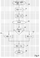
- FIG. 4 is a simplified flow diagram of one embodiment of the protection method according to the invention.
- Positioning for all the circuits connected in parallel for testing by a spike card 1, their respective pads 37 in an inactive state (for example, low).
- test can then begin (block 53, TEST). This test is for example the test conducted conventionally for the type of circuit considered.
- the SEL signal remains in the active default state (step 52 does not succeed).
- test and protection phase is then completed (block 58, END).
- test sequences may be provided.
- an advantage of the above sequence is to allow the use of pad 37 during the test phase.
- the circuits undergo the usual treatments.
- all circuits considered defective have their safety function completely invalid. Indeed, thanks to the breakdown of the fuse, the application of a voltage on the power supply of the circuit will not allow it to start, the signal VAL inactivating permanently and irreversibly, regardless of the subsequent state of the bit SEL , an element essential to the operation of the circuit or at least its secure function.
- the interpretation of the signal VAL or its obtaining logic is such that, after manufacture, the application of a signal on the stud 37 inevitably leads to a blocking of the circuit.
- an attacker manages to access the pad yet inaccessible from outside the integrated circuit it does not allow him to start the circuit or the secure function.
- the default state of the signal SEL is its active state, all the circuits are found for the rest of their life with a switch 38 closed. Therefore, bias the pad 37 in the life of the circuit slams the fuse and blocks the circuit.
- An advantage of the present invention is that the protection element 30 has, because of its simplicity, little risk of itself being defective.
- the active default state of the SEL signal contributes to its security. If necessary, several elements 30 may be provided in parallel to further reduce the risks.
- the present invention is susceptible of various variations and modifications which will be apparent to those skilled in the art.
- the choice of the type of fuse element and the action performed by the protection circuit depends on the application and is within the abilities of those skilled in the art from the functional indications given above.
- the invention has been described in relation to an example in which the integrated circuits are tested in groups, the invention is also applicable if the tests are carried out individually for each circuit of the wafer, the switch of selection 38 and the register 45 then being optional, the programming of the fuse element 31 can be performed by simply applying a signal on the pad 37.
Landscapes
- Engineering & Computer Science (AREA)
- Physics & Mathematics (AREA)
- General Physics & Mathematics (AREA)
- Computer Security & Cryptography (AREA)
- General Engineering & Computer Science (AREA)
- Semiconductor Integrated Circuits (AREA)
- Testing Or Measuring Of Semiconductors Or The Like (AREA)
Abstract
L'invention concerne un procédé et un circuit de protection d'au moins un élément (41) d'un circuit intégré (20), conditionnant le fonctionnement de l'élément à protéger, à l'état d'un signal (VAL) conditionné par un élément à programmation irréversible dont l'état est fixé lors d'un test sous pointes du circuit intégré.
Description
- La présente invention concerne de façon générale les circuits intégrés et plus particulièrement la protection d'informations contenues dans des puces de circuits intégrés rejetées lors de tests des circuits.
- L'invention s'applique plus particulièrement aux circuits contenant un microcontrôleur.
- La fabrication des circuits intégrés s'effectue par plaquettes (wafers) contenant plusieurs circuits. Une fois fabriquées, les plaquettes sont testées, c'est-à-dire que les différents circuits subissent une série de tests fonctionnels au moyen d'outils de test du type à cartes à pointes. Ces tests permettent d'éliminer les circuits défaillants avant les étapes de mise en boîtier.
- En pratique, les circuits sont testés les uns après les autres ou par groupes et ceux qui sont identifiés comme défaillants sont marqués (généralement au moyen d'une goutte d'encre). Par la suite, une fois la plaquette découpée pour individualiser les circuits, le marquage est détecté optiquement pour rejeter les circuits défaillants. En fait, ces circuits sont laissés sur un disque support (tape) servant à la découpe d'où seuls sont prélevés pour mise en boîtier les circuits corrects.
- Un problème apparaît lorsque les circuits intégrés contiennent, par fabrication, des informations considérées comme sensibles ou devant rester secrètes. Il peut s'agir de clés sécrètes ou de fonctions (algorithmes de calcul) spécifiques qui sont fixées à la fabrication (par exemple, par masque).
- Les éléments secrets sont présents à la fois dans les circuits valables et dans les circuits défaillants. Il se pose alors un problème de la destination des circuits défaillants qui doivent être détruits pour éviter que les secrets qu'ils contiennent puissent être percés par des utilisateurs indélicats (pirates) récupérant les circuits défectueux. En effet, les défauts d'un circuit peuvent être suffisants pour empêcher un fonctionnement correct sans pour autant rendre impossible l'accès aux informations sensibles qu'il contient (par exemple, la lecture des zones de mémoire morte dans lesquelles ont été stockées, par fabrication, des clés secrètes).
- Ce problème devient de plus en plus sensible avec la dispersion des lieux de fabrications des circuits intégrés qui entraîne que les plaquettes et circuits sont souvent traités par des sous-traitants plus ou moins contrôlables. Par exemple, l'envoi de plaquettes entières une fois testées à un sous-traitant pour découpe et mise en boîtier pose le problème de s'assurer que les circuits "encrés" soient bien détruits.
- Pour atteindre tout ou partie de ces objets ainsi que d'autres, la présente invention prévoit un procédé de protection d'au moins un élément d'un circuit intégré, consistant à conditionner le fonctionnement de l'élément à protéger, à l'état d'un signal conditionné par un élément à programmation irréversible dont l'état est fixé lors d'un test sous pointes du circuit intégré.
- Selon un mode de mise en oeuvre de la présente invention, l'état de l'élément de programmation est fixé par application d'un signal de programmation sur un plot que comporte le circuit intégré et qui n'est pas destiné à être accessible de l'extérieur une fois le circuit en boîtier.
- Selon un mode de mise en oeuvre de la présente invention, un circuit de protection du circuit intégré est sélectionnable par un signal contenu dans un registre d'activation de l'élément à programmation irréversible.
- L'invention prévoit également un circuit intégré, comportant au moins un élément de protection d'accès à au moins une fonction du circuit, dont l'état est programmé de façon irréversible par application d'un signal sur un plot que comporte le circuit lors d'un test sous pointes.
- Selon un mode de réalisation de la présente invention, ledit élément de protection comporte au moins :
- un élément à programmation irréversible ;
- un élément de lecture de l'état de l'élément de programmation ; et
- un élément de sélection du circuit de protection.
- Ces objets, caractéristiques et avantages, ainsi que d'autres de la présente invention seront exposés en détail dans la description suivante de modes de réalisation particuliers faite à titre non-limitatif en relation avec les figures jointes parmi lesquelles :
- la figure 1 représente, de façon très schématique, un exemple de système de test de circuits intégrés en plaquette du type auquel s'applique la présente invention ;
- la figure 2 représente un mode de réalisation d'un circuit de protection d'un circuit intégré selon la présente invention ;
- la figure 3 représente partiellement un mode de réalisation d'une architecture de circuit intégré selon la présente invention ; et
- la figure 4 est un organigramme simplifié illustrant un mode de mise en oeuvre du procédé de protection d'un circuit intégré selon l'invention.
- Les mêmes éléments ont été désignés par les mêmes références aux différentes figures. Pour des raisons de clarté, seuls les éléments qui sont nécessaires à la compréhension de l'invention ont été représentés et seront décrits par la suite. En particulier, l'outil de test par plaquettes entières n'a pas été détaillé, l'invention étant compatible avec l'utilisation d'outils classiques. De plus, la structure interne du circuit intégré à protéger n'a été détaillée que pour exposer certains exemples de réalisation.
- La figure 1 représente, de façon très schématique et sous forme de blocs, un exemple de système de test auquel s'applique la présente invention. Un tel système est basé sur l'utilisation d'une carte à pointes 1 comportant un ou plusieurs sites de test, portée par une tête de test 10 d'un outil, sur un support 11 duquel repose une plaquette W de circuits intégrés à tester. La tête 10 de test est articulée au moins verticalement par rapport au support 11 de manière à pouvoir approcher et écarter la carte à pointes 1 après introduction d'une nouvelle plaquette W à tester. L'ensemble est généralement commandé par un élément informatique, par exemple, un microordinateur 12 ou analogue pourvu d'une unité centrale 13, d'un écran 14, d'un clavier 15, et d'une souris 16 ou autres moyens de commande et de saisie.
- L'objectif du système de test de la figure 1 est de tester un ou plusieurs des circuits intégrés 20 réalisés dans la plaquette W au moyen de contacts assurés par des pointes 17 de la carte 1. Ces pointes 17 sont réparties selon le motif de plots de contact (non représentées en figure 1) des circuits intégrés à tester. Les tests fonctionnels comprennent, par exemple, des tests de continuité électrique, des tests de mémorisation correcte d'informations, d'exécution correcte de calculs, etc. qui dépendent de la structure du circuit intégré 20 et de sa destination (l'application ou les applications auxquelles il est destiné).
- Une fois testés, les différents circuits intégrés 20 portés par une même plaquette W sont découpés puis mis en boîtier.
- Pour éviter que des informations sensibles (par exemple, des clés ou des algorithmes) intégrées dans les circuits 20 soient susceptibles d'être piratées à partir de circuits déclarés défectueux, l'invention prévoit, selon un mode de réalisation préféré, d'invalider le fonctionnement de tout ou partie du circuit intégré par une commande électrique effectuée en fin de test sous pointes.
- La figure 2 illustre, de façon partielle et très schématique, un mode de réalisation d'un circuit 30 de protection d'au moins une zone sécurisée d'un circuit intégré 20 selon la présente invention. Le circuit 30 est destiné à fournir un signal VAL conditionnant le fonctionnement d'une zone sécurisée du circuit (non représentée en figure 2) dont l'état est conditionné par l'état d'un élément fusible ou anti-fusible 31 (F), ou équivalent. Par équivalent à élément fusible 31, on entend tout élément de conduction électrique dont l'état conducteur ou l'amplitude de conduction peut être modifiée de façon irréversible indépendamment de l'alimentation du circuit.
- Dans l'exemple fonctionnel de la figure 2, l'élément fusible 31 est, par exemple, un élément résistif formant avec un autre élément résistif 32 un pont diviseur entre deux bornes 33 et 34 d'application d'une tension d'alimentation Vcc, le point milieu 35 de cette association en série étant relié en entrée d'un élément de lecture 36 (par exemple, un inverseur) dont la sortie fournit le signal VAL. Selon l'état de l'élément fusible 31, l'état de sortie du signal VAL lorsque le circuit est soumis à une tension d'alimentation Vcc est bas ou haut. Ce signal peut alors servir à conditionner le fonctionnement d'une zone protégée du circuit ou de l'intégralité du circuit.
- La programmation de l'élément fusible 31 en fin de test sous pointes est, selon ce mode de réalisation de l'invention, effectuée au moyen d'un plot 37 (P) prévu dans la surface du circuit intégré 20 pour recevoir une pointe 17 de l'outil de test, le plot 37 n'étant pas accessible de l'extérieur du circuit, une fois le circuit intégré mis en boîtier.
- De préférence, le plot 37 relie le point 35 par l'intermédiaire d'un interrupteur 38 commandé par un signal SEL de sélection du circuit 30. Le signal SEL de sélection et l'interrupteur 38 servent notamment à effectuer des tests en parallèle de plusieurs circuits intégrés et à sélectionner, en fin de test, ceux dont l'élément fusible 31 doit être programmé ou non comme on le verra par la suite.
- L'élément fusible 31 est, de préférence, un élément à programmation électrique sous l'application d'un courant ou d'une tension sur le plot 37 alors que l'interrupteur 38 est fermé. La programmation de l'élément 31 peut avoir pour effet d'ouvrir ou de fermer le circuit électrique qu'il définit et plus généralement d'en augmenter ou d'en diminuer la résistance de façon à conditionner l'état du signal VAL de sortie de l'élément de lecture 36.
- Tout élément dont un changement d'état est irréversible pourra être utilisé. Il pourra s'agir d'un claquage d'un fusible par effet Joule, d'un fusible métallique ou en silicium polycristallin, d'une destruction d'une jonction par effet thyristor, d'une modification de la caractéristique résistive d'un élément due à un courant important, d'un claquage d'oxyde par champ électrique (antifusible MOS), etc.
- La figure 3 illustre un exemple d'architecture partielle d'un circuit intégré selon un mode de réalisation de l'invention. Dans un mode de réalisation préféré, le circuit intégré 20 à protéger, ou dont une fonction de sécurité 41 (SEC FCT) est à protéger, comporte une unité centrale de traitement 42 (CPU) chargée d'exécuter des programmes stockés, par exemple, dans une mémoire morte 43 (ROM). L'ensemble des éléments de calcul communiquent par un ou plusieurs bus 44.
- Pour la mise en oeuvre de ce mode de réalisation de l'invention, un circuit 30 (PROT) de protection, par exemple du type de celui décrit en relation avec la figure 2, est intégré dans le circuit 20. Dans le mode de réalisation de la figure 3, le signal SEL est fourni par un registre 45 (REG) programmable par le microprocesseur 42 et une entrée 46 du circuit 30, correspondant à la borne de l'interrupteur 38 (figure 2) dont l'état est conditionné par le signal SEL et qui est reliée au plot 37, se trouve également reliée à un circuit 47 communiquant avec le bus 44 pour recevoir des signaux provenant de l'unité centrale 42. Le circuit 47 constitue le circuit d'interface logique (LPAD) du plot 37.
- Le signal VAL fourni par le circuit 30 est envoyé sur la fonction sécurisée 41 du circuit intégré 20. L'action prise pour bloquer le circuit si le fusible contenu dans le circuit 30 a été programmé (claqué) dépend du contenu du circuit 41 et du type de données (clé ou programme) à protéger. Par exemple, le signal VAL sert à :
- réinitialiser l'unité centrale 42 afin d'arrêter son signal d'horloge ;
- programmer dans un état inactif un signal interne au circuit 41 (signal de réinitialisation, d'horloge, bus de données connecté directement à la masse ou d'adresse, etc.) ;
- court-circuiter l'alimentation du circuit intégré ;
- bloquer un canal quelconque de communication, etc.
- Le registre 45 sert de registre d'activation-désactivation du claquage du fusible du circuit 30. Ce registre est préférentiellement commandé par l'unité centrale 42, ce qui permet de désactiver le claquage du fusible pendant la phase de test ou si le circuit a été testé de façon correcte.
- La figure 4 est un organigramme simplifié d'un mode de mise en oeuvre du procédé de protection selon l'invention.
- Au démarrage d'un test d'une plaquette (bloc 50, START TEST) l'état du signal SEL de tous les circuits est actif (SEL = 1), ce qui représente l'état par défaut.
- On positionne (bloc 51, PAD = 0), pour tous les circuits connectés en parallèle pour test par une carte à pointes 1, leurs plots 37 respectifs dans un état inactif (par exemple, bas). L'unité centrale 42 du circuit intégré ou un organe central de commande externe de l'outil de test positionne (bloc 52, SEL = 0) par ailleurs le bit de sélection conditionnant l'état de l'interrupteur 38 à l'état inactif.
- Le test proprement dit peut alors débuter (bloc 53, TEST). Ce test est par exemple le test conduit classiquement pour le type de circuit considéré.
- En fin de test, on vérifie (bloc 54, TEST OK ?) que le test conduit à un fonctionnement correct du circuit. Dans l'affirmative (bloc 55, SEL = 0), l'unité centrale 42 laisse le bit SEL contenu dans le registre 45 (figure 3) à l'état inactif. Si le test 54 est négatif (circuit défectueux), l'unité centrale 42 positionne (bloc 56, SEL = 1) le registre 45 dans l'état opposé et le signal de sélection SEL se trouve, pour le circuit intégré considéré de la plaquette, dans un état actif.
- Pour tous les circuits (non fonctionnels) pour lesquels aucune programmation ne fonctionne, le signal SEL reste à l'état par défaut actif (l'étape 52 n'aboutit pas).
- Puis (bloc 57, PAD = Vcc), on applique par l'intermédiaire de la carte à pointes, une tension de programmation (par exemple la tension Vdd) sur les plots 37 de tous les circuits testés en parallèle. Par les programmations respectives des registres 45 des différents circuits, seuls ceux dont le signal SEL est à l'état actif vont subir une programmation de leur élément fusible.
- La phase de test et de protection est alors terminée (bloc 58, END).
- D'autres séquences de test peuvent être prévues. Toutefois, un avantage de la séquence ci-dessus est de permettre l'utilisation du plot 37 pendant la phase de test.
- Par la suite, les circuits subissent les traitements habituels. On peut par exemple maintenir un encrage des circuits défectueux pour préserver la reconnaissance optique lors de leur découpe et assemblage. Toutefois, tous les circuits considérés comme défectueux ont leur fonction de sécurité complètement invalide. En effet, grâce au claquage du fusible, l'application d'une tension électrique sur l'alimentation du circuit ne lui permettra pas de démarrer, le signal VAL inactivant de façon permanente et irréversible, quel que soit l'état ultérieur du bit SEL, un élément indispensable au fonctionnement du circuit ou au moins de sa fonction sécurisée.
- Dans un mode de réalisation préféré de l'invention, l'interprétation du signal VAL ou sa logique d'obtention est telle que, après fabrication, l'application d'un signal sur le plot 37 conduit forcément à un blocage du circuit. Ainsi, même si un pirate parvient à accéder au plot pourtant inaccessible de l'extérieur du circuit intégré, cela ne lui permet pas de démarrer le circuit ou la fonction sécurisée. C'est le cas du mode de réalisation décrit en relation avec la figure 4 où l'état par défaut du signal SEL étant son état actif, tous les circuits se retrouvent pour le reste de leur vie avec un interrupteur 38 fermé. Par conséquent, polariser le plot 37 dans la vie du circuit claque le fusible et bloque le circuit.
- Un avantage de la présente invention est que l'élément de protection 30 a, grâce à sa simplicité, peu de risque d'être lui-même défectueux. De plus, l'état par défaut actif du signal SEL participe à sa sécurité. Le cas échéant, plusieurs éléments 30 peuvent être prévus en parallèles pour réduire encore les risques.
- Bien entendu, la présente invention est susceptible de diverses variantes et modifications qui apparaîtront à l'homme de l'art. En particulier, le choix du type d'élément fusible et de l'action effectuée par le circuit de protection dépend de l'application et est à la portée de l'homme du métier à partir des indications fonctionnelles données ci-dessus. De plus, bien que l'invention ait été décrite en relation avec un exemple dans lequel les circuits intégrés sont testés par groupes, l'invention s'applique également si les tests sont effectués individuellement pour chaque circuit de la plaquette, l'interrupteur de sélection 38 et le registre 45 étant alors optionnels, la programmation de l'élément fusible 31 pouvant s'effectuer par simple application d'un signal sur le plot 37.
Claims (5)
- Procédé de protection d'au moins un élément (41) d'un circuit intégré (20), caractérisé en ce qu'il consiste à conditionner le fonctionnement de l'élément à protéger, à l'état d'un signal (VAL) conditionné par un élément à programmation irréversible (31) dont l'état est fixé lors d'un test sous pointes du circuit intégré.
- Procédé selon la revendication 1, dans lequel l'état de l'élément de programmation (31) est fixé par application d'un signal de programmation sur un plot (37) que comporte le circuit intégré et qui n'est pas destiné à être accessible de l'extérieur une fois le circuit en boîtier.
- Procédé selon la revendication 1, dans lequel un circuit (30) de protection du circuit intégré est sélectionnable par un signal (SEL) contenu dans un registre (35) d'activation de l'élément à programmation irréversible.
- Circuit intégré (20), caractérisé en ce qu'il comporte au moins un élément (30) de protection d'accès à au moins une fonction (41) du circuit, dont l'état est programmé de façon irréversible par application d'un signal sur un plot (37) que comporte le circuit lors d'un test sous pointes.
- Circuit selon la revendication 4, dans lequel ledit élément de protection (30) comporte au moins :un élément (31) à programmation irréversible ;un élément (36) de lecture de l'état de l'élément de programmation ; etun élément (38) de sélection du circuit de protection.
Applications Claiming Priority (1)
| Application Number | Priority Date | Filing Date | Title |
|---|---|---|---|
| FR0452964A FR2879296A1 (fr) | 2004-12-14 | 2004-12-14 | Invalidation d'un circuit integre |
Publications (1)
| Publication Number | Publication Date |
|---|---|
| EP1674875A1 true EP1674875A1 (fr) | 2006-06-28 |
Family
ID=34952147
Family Applications (1)
| Application Number | Title | Priority Date | Filing Date |
|---|---|---|---|
| EP05112078A Withdrawn EP1674875A1 (fr) | 2004-12-14 | 2005-12-13 | Invalidation d'un circuit intégré |
Country Status (3)
| Country | Link |
|---|---|
| US (1) | US20060124928A1 (fr) |
| EP (1) | EP1674875A1 (fr) |
| FR (1) | FR2879296A1 (fr) |
Citations (6)
| Publication number | Priority date | Publication date | Assignee | Title |
|---|---|---|---|---|
| JPS62136070A (ja) * | 1985-12-09 | 1987-06-19 | Nec Corp | 半導体装置の製造方法 |
| US5671281A (en) * | 1993-03-11 | 1997-09-23 | International Business Machines Corporation | Self modifying access code for altering capabilities |
| EP0920057A2 (fr) * | 1989-01-12 | 1999-06-02 | General Instrument Corporation | Protection d'une puce à circuit intégré à l'aide d'un écran conducteur |
| US5981971A (en) * | 1997-03-14 | 1999-11-09 | Kabushiki Kaisha Toshiba | Semiconductor ROM wafer test structure, and IC card |
| EP1111618A1 (fr) * | 1999-12-22 | 2001-06-27 | Texas Instruments Incorporated | Architecture de fusible électrique protégée en lecture et écriture |
| JP2001291751A (ja) * | 2000-04-06 | 2001-10-19 | Sony Corp | 半導体装置 |
Family Cites Families (1)
| Publication number | Priority date | Publication date | Assignee | Title |
|---|---|---|---|---|
| US6608792B2 (en) * | 2000-11-09 | 2003-08-19 | Texas Instruments Incorporated | Method and apparatus for storing data in an integrated circuit |
-
2004
- 2004-12-14 FR FR0452964A patent/FR2879296A1/fr not_active Withdrawn
-
2005
- 2005-12-13 EP EP05112078A patent/EP1674875A1/fr not_active Withdrawn
- 2005-12-14 US US11/302,620 patent/US20060124928A1/en not_active Abandoned
Patent Citations (6)
| Publication number | Priority date | Publication date | Assignee | Title |
|---|---|---|---|---|
| JPS62136070A (ja) * | 1985-12-09 | 1987-06-19 | Nec Corp | 半導体装置の製造方法 |
| EP0920057A2 (fr) * | 1989-01-12 | 1999-06-02 | General Instrument Corporation | Protection d'une puce à circuit intégré à l'aide d'un écran conducteur |
| US5671281A (en) * | 1993-03-11 | 1997-09-23 | International Business Machines Corporation | Self modifying access code for altering capabilities |
| US5981971A (en) * | 1997-03-14 | 1999-11-09 | Kabushiki Kaisha Toshiba | Semiconductor ROM wafer test structure, and IC card |
| EP1111618A1 (fr) * | 1999-12-22 | 2001-06-27 | Texas Instruments Incorporated | Architecture de fusible électrique protégée en lecture et écriture |
| JP2001291751A (ja) * | 2000-04-06 | 2001-10-19 | Sony Corp | 半導体装置 |
Non-Patent Citations (2)
| Title |
|---|
| PATENT ABSTRACTS OF JAPAN vol. 011, no. 359 (E - 559) 21 November 1987 (1987-11-21) * |
| PATENT ABSTRACTS OF JAPAN vol. 2002, no. 02 2 April 2002 (2002-04-02) * |
Also Published As
| Publication number | Publication date |
|---|---|
| FR2879296A1 (fr) | 2006-06-16 |
| US20060124928A1 (en) | 2006-06-15 |
Similar Documents
| Publication | Publication Date | Title |
|---|---|---|
| JP4897279B2 (ja) | アーキテクチャを隠し、リバースエンジニアリングを防止し、デバイスを動作不能にするための、電気的にプログラム可能なヒューズの使用 | |
| EP0597745B1 (fr) | Circuit à fusible, pour circuit intégré | |
| EP1267248B1 (fr) | Stockage protégé d'une donnée dans un circuit intégré | |
| KR100721895B1 (ko) | 판독/기입 방지의 전기적 퓨즈 구조 | |
| FR2746962A1 (fr) | Dispositif de securite d'une pastille semi-conductrice | |
| CN101965637A (zh) | 具有mosfet熔丝元件的集成电路 | |
| JP2010507255A (ja) | 複数の論理素子を含むワンタイムプログラマブルロジックビット | |
| EP2078304A1 (fr) | Procédé de fourniture d'une programmation par champ optimale de fusibles électroniques | |
| US9762391B2 (en) | Chip authentication technology using carbon nanotubes | |
| US20050212090A1 (en) | Integrated circuit | |
| US20060289658A1 (en) | Processor circuit and method of allocating a logic chip to a memory chip | |
| JP3544168B2 (ja) | 電子装置及びその製造方法 | |
| FR2879296A1 (fr) | Invalidation d'un circuit integre | |
| EP2333703B1 (fr) | Composant électronique apte à détecter des attaques actives | |
| US7518899B2 (en) | Method of providing optimal field programming of electronic fuses | |
| FR2960327A1 (fr) | Procede et systeme d'acces a un circuit integre comprenant une cle personnelle d'authentification | |
| Zonenberg et al. | Extraction of Secrets from 40nm {CMOS} Gate Dielectric Breakdown Antifuses by {FIB} Passive Voltage Contrast | |
| CN115878193A (zh) | 一种芯片启动方法及装置 | |
| GB2349491A (en) | Programmable semiconductor device providing security of circuit information | |
| FR2860342A1 (fr) | Circuit integre a dispositif formant capteur de rayonnement | |
| EP3391228A1 (fr) | Procédé d'écriture dans une mémoire non-volatile d'une entité électronique et entité électronique associée | |
| EP0675441A1 (fr) | Dispositif matriciel de fusibles de redondance pour mémoire intégrée et procédé de mise en oeuvre | |
| US6704676B2 (en) | Method and circuit configuration for identifying an operating property of an integrated circuit | |
| EP1873537A1 (fr) | Qualification d'un détecteur de pics parasites dans l'alimentation d'un circuit intégré | |
| EP1715436A2 (fr) | Protection du déroulement d'un programme exécuté par un circuit intégré ou de données contenues dans ce circuit |
Legal Events
| Date | Code | Title | Description |
|---|---|---|---|
| PUAI | Public reference made under article 153(3) epc to a published international application that has entered the european phase |
Free format text: ORIGINAL CODE: 0009012 |
|
| AK | Designated contracting states |
Kind code of ref document: A1 Designated state(s): AT BE BG CH CY CZ DE DK EE ES FI FR GB GR HU IE IS IT LI LT LU LV MC NL PL PT RO SE SI SK TR |
|
| AX | Request for extension of the european patent |
Extension state: AL BA HR MK YU |
|
| AKX | Designation fees paid | ||
| REG | Reference to a national code |
Ref country code: DE Ref legal event code: 8566 |
|
| STAA | Information on the status of an ep patent application or granted ep patent |
Free format text: STATUS: THE APPLICATION IS DEEMED TO BE WITHDRAWN |
|
| 18D | Application deemed to be withdrawn |
Effective date: 20061229 |