EP1672790A2 - Surface acoustic wave device and method of manufacturing the same, ic card, and mobile electronic apparatus - Google Patents
Surface acoustic wave device and method of manufacturing the same, ic card, and mobile electronic apparatus Download PDFInfo
- Publication number
- EP1672790A2 EP1672790A2 EP05027601A EP05027601A EP1672790A2 EP 1672790 A2 EP1672790 A2 EP 1672790A2 EP 05027601 A EP05027601 A EP 05027601A EP 05027601 A EP05027601 A EP 05027601A EP 1672790 A2 EP1672790 A2 EP 1672790A2
- Authority
- EP
- European Patent Office
- Prior art keywords
- cover
- electrodes
- saw
- saw chip
- metal bonding
- Prior art date
- Legal status (The legal status is an assumption and is not a legal conclusion. Google has not performed a legal analysis and makes no representation as to the accuracy of the status listed.)
- Withdrawn
Links
Images







Classifications
-
- H—ELECTRICITY
- H03—ELECTRONIC CIRCUITRY
- H03H—IMPEDANCE NETWORKS, e.g. RESONANT CIRCUITS; RESONATORS
- H03H9/00—Networks comprising electromechanical or electro-acoustic elements; Electromechanical resonators
- H03H9/02—Details
- H03H9/05—Holders or supports
- H03H9/10—Mounting in enclosures
- H03H9/1064—Mounting in enclosures for surface acoustic wave [SAW] devices
- H03H9/1092—Mounting in enclosures for surface acoustic wave [SAW] devices the enclosure being defined by a cover cap mounted on an element forming part of the surface acoustic wave [SAW] device on the side of the IDT's
-
- H—ELECTRICITY
- H03—ELECTRONIC CIRCUITRY
- H03H—IMPEDANCE NETWORKS, e.g. RESONANT CIRCUITS; RESONATORS
- H03H9/00—Networks comprising electromechanical or electro-acoustic elements; Electromechanical resonators
- H03H9/25—Constructional features of resonators using surface acoustic waves
-
- H—ELECTRICITY
- H03—ELECTRONIC CIRCUITRY
- H03H—IMPEDANCE NETWORKS, e.g. RESONANT CIRCUITS; RESONATORS
- H03H3/00—Apparatus or processes specially adapted for the manufacture of impedance networks, resonating circuits, resonators
- H03H3/007—Apparatus or processes specially adapted for the manufacture of impedance networks, resonating circuits, resonators for the manufacture of electromechanical resonators or networks
- H03H3/08—Apparatus or processes specially adapted for the manufacture of impedance networks, resonating circuits, resonators for the manufacture of electromechanical resonators or networks for the manufacture of resonators or networks using surface acoustic waves
-
- H—ELECTRICITY
- H03—ELECTRONIC CIRCUITRY
- H03H—IMPEDANCE NETWORKS, e.g. RESONANT CIRCUITS; RESONATORS
- H03H9/00—Networks comprising electromechanical or electro-acoustic elements; Electromechanical resonators
- H03H9/02—Details
Definitions
- the present invention relates to a SAW device such as a surface acoustic wave (SAW) such as a resonator, a filter, and oscillator and a method of manufacturing the same.
- a SAW device such as a surface acoustic wave (SAW) such as a resonator, a filter, and oscillator and a method of manufacturing the same.
- the present invention relates to an IC card and a mobile electronic apparatus having the SAW device.
- SAW devices having SAW elements including IDTs (comb-shaped transducers : Inter Digital Transducers) constructed with alternate finger electrode formed on a surface of a piezoelectric substrate and reflectors and using surface acoustic wave excited from the IDTs have been widely used for various electronic apparatuses.
- IDTs comb-shaped transducers : Inter Digital Transducers
- thinner SAW devices have been required in order to be used for small-sized thin information apparatuses such as an IC card.
- a SAW device in the related art is constructed by hermetically sealing SAW elements in a package which is formed by bonding a metal lid to a base made of a ceramic material with seam-welding.
- bonding pads of an IDT formed on a surface of a piezoelectric substrate is electrically connected to connection terminals of the package by using bonding wires (for example, see JP-A-2002-16476 and JP-A-2003-87072).
- bonding wires for example, see JP-A-2002-16476 and JP-A-2003-87072.
- the number of parts is too large, and the construction is too complicated.
- a large space is needed in the package, so that there is a limitation on implementing a small-sized thin SAW device.
- a double-layered surface acoustic wave apparatus including a surface acoustic wave element having IDT electrodes, extraction electrodes, and positive electrode bonding portions on a substrate and a cover plate constructed with a glass plate having through-holes provided with external electrodes, wherein the extraction electrodes and the external electrodes are electrically connected, and wherein the cover plate and the positive bonding portion are bonded to seal the IDT electrodes (for example, see JP-A-8-213874).
- the base and the bonding wires mounted on the SAW element are omitted, a whole construction can be simplified-, and a small-sized thin product can be obtained.
- production cost can be reduced, and frequency characteristics can be stabilized.
- the SAW element and the cover plate are bonded by aligning and closely adhering the extraction electrodes and the through-holes at the positive electrode bonding portion, and after, the external electrodes are formed at the through-holes and peripheral portions thereof and electrically connected to the excitation by using a sputtering process in a vacuum ambience.
- the extraction electrodes are made of aluminum, the surface thereof is naturally oxidized due to air contact. Therefore, after the positive electrode bonding between the SAW element and the cover plate, although the external electrodes are formed in vacuum, sufficient electrical conduction to the extraction electrodes cannot be ensured.
- the sealing of the through-holes are performed by forming the extraction electrodes and the electrode of the positive electrode bonding portion with the same film thickness to not generate gaps between the extraction electrodes and the through-holes and forming the external extrudes on inner sides of the through-holes.
- the double-layered SAW device is a surface mounting type one
- the external electrodes formed on a surface of the cover plate are directly adhered on a surface of a print board or the like with a solder, an adhesive, or the like.
- the mounting area is reduced. Therefore, it may be difficult to mount the SAW device in a good state and obtain a sufficient adhesive strength after the mounting thereof, so that sufficient mechanical strength against an external force such as bending cannot be secured.
- the present invention has been considered the above circumstance, and it is an advantage of the invention to provide a double-layered SAW device capable of directly bonding a SAW chip and a cover to seal IDT electrodes or the like formed on a surface of the SAW chip and electrically connecting the IDT electrodes and external electrodes on as surface of the cover through through-holes formed in the cover, thereby obtaining a thin product, securing electrical conduction between the IDT electrodes and the external electrodes, and securely hermetically sealing the through-holes.
- a surface acoustic wave device comprising: a SAW chip having IDT electrodes disposed on a main surface of a piezoelectric substrate, extraction electrodes extracted from the IDT electrodes, and a metal bonding portion disposed along the entire periphery of the main surface of the piezoelectric substrate; and a cover having through-holes disposed on an insulating substrate at positions corresponding to the extraction electrodes of the SAW chip, a metal bonding portion disposed along the entire periphery of a lower surface of the insulating substrate, connection electrodes disposed on the lower surface of the insulating substrate along circumferences of openings of the through-holes, and external electrodes disposed on an upper surface of the insulating substrate in peripheries of openings of the through-holes; wherein the SAW chip and the cover are bonded in a body by bonding the metal bonding portion of the SAW chip and the metal bonding portion of the cover and bonding the extraction electrodes of the
- connection electrodes disposed in the peripheries of the openings of the through-holes for electrode extraction disposed in the cover and the extraction electrodes of the SAW chip as well as by bonding the metal bonding portions disposed in peripheries of the SAW chip and the cover, it is possible to secure electrical conduction between the IDT electrodes and the external electrodes and to more securely hermetically seal the interior of the SAW device.
- metal bonding portions disposed in peripheries of the SAW chip and the cover it is possible to secure electrical conduction between the IDT electrodes and the external electrodes and to more securely hermetically seal the interior of the SAW device.
- the thickness of the metal bonding portion of the SAW chip and the metal bonding portion of the cover in the bonded state and the thickness of the extraction electrodes of the SAW device and the connection electrodes of the cover in the bonded state may be determined to be larger than the thickness of the IDT electrodes. Therefore, the space between the SAW chip and the cover can be larger than the thickness of the IDT electrodes, and the gap between the IDT electrode and the cover can be secured. As a result, since the IDT electrodes are sealed in the SAW device so as not to contact the cover, it is possible to secure predetermined operations.
- the space between the SAW chip and the cover in the bonded state may be equal to the thickness of the IDT electrodes. Therefore, since the gap between the upper ends of the IDT electrodes and the lower surface of the cover can be removed by contacting the upper ends of the IDT electrodes and the lower surface of the cover, the thickness of the SAW device can be reduced down to a minimum thickness.
- the cover may further comprise concave portions disposed at positions at least partially overlapping with the external electrodes on the upper surface of the cover. Therefore, since conductive adhesive such as a solder paste used to mount the SAW resonator on a print board or the like can penetrate into the concave portions, adhesion area can increase. As a result, although the SAW device is manufactured with a small size and a thin thickness, it is possible to secure a sufficient mechanical strength after the mounting thereof.
- the concave portions may be disposed at outer peripheral edges of the cover.
- the SAW device can be supported by the side surfaces at the time of the mounting thereof, so that it is possible to further improve the bonded state and the mechanical strength.
- the concave portions may be coated with metal films. Therefore, since wettability to the concave portions can be improved, a conductive adhesive such as a solder paste can easily penetrate into the concave portions, and surface areas of the external electrodes can increase practically. As a result, it is possible to improve the electrical connection to the print board on which the SAW device is mounted.
- inner circumferential surfaces of the through-holes of the cover may be coated with metal films made of the conductive materials.
- the IDT electrodes and the external electrodes can be electrically connected to each other.
- the metal bonding portion and the extraction electrodes of the SAW chip may be constructed with a Cr/Au film
- the metal bonding portion and the connection electrodes of the cover may be constructed with a Cr/Au film.
- theses components can be bonded with a thermal bonding process.
- the metal bonding portion and the connection electrodes of the cover may have an AuSn alloy film disposed on the Cr/Au film.
- the SAW chip and the cover can be bonded with a thermal pressing process or a eutectic bonding process.
- the surface of the Cr/Au film of the extraction electrodes is not oxidized due to air contact unlike an Al film, it is possible to secure electrical conduction to connection electrode.
- a method of manufacturing a surface acoustic wave device comprising steps of: forming a SAW chip having IDT electrodes disposed on a main surface of a piezoelectric substrate, extraction electrodes extracted from the IDT electrodes, and a metal bonding portion disposed along the entire periphery of the main surface of the piezoelectric substrate; forming a cover having through-holes disposed on an insulating substrate at positions corresponding to the extraction electrodes of the SAW chip, a metal bonding portion disposed along the entire periphery of a lower surface of the insulating substrate, and connection electrodes disposed on the lower surface of the insulating substrate along circumferences of openings of the through-holes; bonding the SAW chip and the cover in a body by bonding the metal bonding portion of the SAW chip and the metal bonding portion of the cover and bonding the extraction electrodes of the SAW chip and the connection electrodes of the cover so as to hermetically seal the IDT electrodes
- the method may further comprise a step of forming concave portions at positions at least partially overlapping with the external electrodes on the upper surface of the cover. It is preferable that the concave portions on the upper surface of the cover are formed by using the same process as the process for forming the through-holes of the cover. As a result, by using the manufacturing process in the related art, it is possible to manufacture a SAW device having a good bonded state and a high mechanical strength after the mounting thereof without increase in the number of processes.
- the IDT electrodes and the external electrodes may be electrically connected to each other by forming metal films made of the conductive materials on inner circumferential surfaces of the through-holes. Since the inner surfaces of the through-holes are constructed with metal films to improve wettability thereto, conductive materials can be easily filled therein. As a result, it is possible to improve reliability of the electrical conduction between the IDT electrodes and the external electrodes and the hermetical sealing of the through-holes.
- the method may further comprise, after the SAW chip and the cover are bonded in a body, a step of polishing a surface of the SAW chip and/or the cover.
- the metal bonding portion and the extraction electrodes of the SAW chip may be formed with a Cr/Au film
- the metal bonding portion and the connection electrodes of the cover may be formed with a Cr/Au film
- the metal bonding portion and the extraction electrodes of SAW chip and the metal bonding portion and the connection electrodes of the cover may be bonded with a thermal pressing process.
- the metal bonding portion and the extraction electrodes of the SAW chip may be formed with a Cr/Au film
- the metal bonding portion and the connection electrodes of the cover may be formed with a Cr/Au film and an AuSn alloy film thereon
- the metal bonding portion and the extraction electrodes of SAW chip and the metal bonding portion and the connection electrodes of the cover may be bonded with a thermal pressing process or an eutectic bonding process.
- the surface of the Cr/Au film is not naturally oxidized due to air contact unlike an Al film, and the Al film is formed later than the Cr/Au film. As a result, although the surface thereof is oxidized due to air contact, the electrical conduction between the extraction electrodes and the connection electrode cannot deteriorate.
- the method may further comprise steps of: forming a SAW chip wafer on which a plurality of the SAW chips are continuously disposed in the step of forming the SAW chip; forming a cover wafer on which a plurality of the covers are continuously disposed in the step of forming the cover; bonding the SAW chip wafer and the cover wafer in a body to form a wafer stacked structure by bonding the metal bonding portions of the SAW chips of the SAW chip wafer and the metal bonding portions of the covers of the cover wafer and bond the extraction electrodes of the SAW chips and the connection electrodes of the covers in the step of bonding the SAW chip and the cover in a body; and dicing the wafer stacked structure into individual SAW devices.
- an IC card which the aforementioned surface acoustic wave device is built in. As a result, it is possible to implement a desired thin IC card.
- a mobile electronic apparatus which the aforementioned surface acoustic wave device is built in. As a result, it is possible to implement a much thinner mobile electronic apparatus.
- Fig. 1A is a plan view showing a SAW resonator according to a first embodiment of the invention
- Fig. 1B is a cross sectional view taken along line I-I of Fig. 1A.
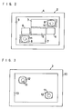
- Fig. 2 is a plan view showing a SAW chip of Figs. 1A and 1B.
- Fig. 3 is a bottom view showing a bonding surface of a cover of Figs. 1A and 1B.
- Figs. 4A to 4D are partially enlarged cross sectional views of a quartz wafer and a glass wafer for explaining a sequence of processes of a method of manufacturing the SAW of Fig. 1.
- Fig. 5A is a plan view showing a SAW resonator according to a second embodiment of the invention
- Fig. 5B is a cross sectional view taken along line V-V of Fig. 5A.
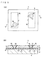
- Fig. 6 is a plan view showing a SAW chip of Figs. 5A and 5B.
- Fig. 7 is a bottom view showing a bonding surface of a cover of Figs. 5A and 5B.
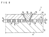
- Fig. 8 is a partially enlarged cross sectional view showing a SAW resonator according to a modified example of the second embodiment.
- Figs. 9A to 9D are partially enlarged cross sectional views of a quartz wafer and a glass wafer for explaining a sequence of processes of a method of manufacturing the SAW of Fig 5.
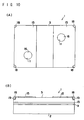
- Fig. 10A is a plan view showing a SAW resonator according to a modified example of the first embodiment, and Fig. 10B is a side view thereof.
- Fig. 11 is a plan view of a SAW resonator having a foot pattern different from that of Figs. 10A and 10B.
- Fig. 12 is a plan view of a SAW resonator in which concave portions having a pattern different from that of Figs. 10A and 10B are disposed.
- Fig. 13 is a plan view of a SAW resonator in which concave portions having another pattern different from that of Figs. 10A and 10B are disposed.
- Fig. 14 is a plan view of a SAW resonator in which concave portions having still another pattern different from that of Figs. 10A and 10B are disposed.
- Fig. 15A is a plan view showing a state where concave portions are formed on a glass wafer in a process for manufacturing the SAW resonator of Figs. 10A and 10B
- Fig. 15B is a plan view showing a state where an electrode film for external electrodes is further formed.
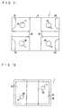
- Fig. 16A is a plan view showing a state where concave portions are formed on a glass wafer in a process for manufacturing the SAW resonator of Fig. 12, and Fig. 16B is a plan view showing a state where an electrode film for external electrodes is further formed.
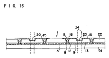
- Figs. 17A and 17B is a cross sectional view of a quartz wafer and a glass wafer for explaining an individualizing process using dicing in a process for manufacturing the SAW resonator of Fig. 12.
- Figs. 1A and 1B show a SAW resonator according to a first embodiment of the invention.
- the SAW resonator 1 has a structure where a SAW chip 2 and a cover 3 are directly bonded.
- the SAW chip 2 is constructed with a rectangular piezoelectric substrate 4, an IDT 5 constructed with a pair of alternate finger electrodes is formed on a central region of an upper surface thereof, and reflectors 6 and 6 are formed at both longitudinal sides of the IDT.
- Lead wires 7 and 7 are extracted from bus bars of the alternate finger electrodes in the opposite directions along longitudinal edges of the piezoelectric substrate 4, and the alternate finger electrodes are connected to extraction electrodes 8 and 8 which are formed at vicinities of diagonal corner portions of the piezoelectric substrate.
- a metal bonding portion 9 is formed along the entire circumference of a peripheral portion of the piezoelectric substrate 4.
- the piezoelectric substrate 4 is made of quartz in the embodiment, other piezoelectric materials such as lithium, tantalate, and lithium niobate may be used.
- the alternate finger electrodes, the reflectors, and lead wires are constructed with an Al film in terms of characteristics, workability, and cost, other conductive metal materials such as an aluminum alloy which are generally used may be used.
- the extraction electrodes 8 and 8 and the metal bonding portion 9 are constructed with a Cr/Au film or a Cr/Ni/Au film at the same height.
- the cover 3 is constructed with a rectangular glass substrate 10, and through-holes 11 and 11 having a shape of a taper directing from an upper surface to a lower surface thereof are formed.
- the through-holes 11 and 11 are disposed in the diagonal direction to correspond to the extraction electrodes 8 and 8 of the SAW chip 2, so that it is possible to reduce an outer dimension and to easily secure a pitch dimension of the through-holes.
- connection electrodes 12 and 12 having a shape corresponding to the extraction electrodes 8 and 8 of the SAW chip 2 are formed over the entire circumferences of the opening peripheries of the though-holes.
- a metal bonding portion 13 is formed on the lower surface of the glass substrate 10 along the entire circumference of a peripheral portion thereof.
- the through-holes 11 and 11 and inner circumferential surfaces of the connection electrodes 12 and 12 which are continuous with the through-holes are coated with metal films 14 and 14 made of a conductive material.
- external electrodes 15 and 15 are formed in the opening peripheries of the through-holes. The external electrodes 15 and 15 are electrically connected to the corresponding connection electrodes 12 and 12 through the metal films 14 and 14 of the through-holes adjacent to the external electrodes.
- the glass substrate 10 is made of soda glass having thermal expansion coefficient which is close to that of the quartz of the piezoelectric substrate 4.
- the connection electrodes 12 and 12 and the metal bonding portion 13 are constructed with a Cr/Au film or a Cr/Ni/Au film at the same height.
- the metal films 14 and 14 and the external electrodes 15 and 15 are constructed with a Cr/Au film or a Cr/Ni/Au film.
- the cover 3 may be made of other glass materials or insulating materials having a thermal expansion coefficient which is equal to or approximate to that of quartz or the quart which is the same as that of the piezoelectric substrate 4.
- the cover 3 may be constructed with a thin plate made of an insulating material having a thermal expansion coefficient which is equal to or approximate to that of the piezoelectric material.
- the SAW chip 2 and the cover 3 are bonded in a body by thermally pressing the metal bonding portion 9 and the metal bonding portion 13 and thermally pressing the extraction electrodes 8 and 8 and the connection electrodes 12 and 12, and the IDT 5 and the reflectors 6 and 6 are hermetically sealed within a space defined between the SAW chip 2 and the cover 3.
- the thicknesses of the extraction electrodes, the connection electrode, and metal bonding portions 9 and 13 are determined so that a thickness in the bonded states thereof are larger than a thickness of the Al film.
- gaps are defined between the upper ends of the IDT and the reflectors and the lower surface of the cover 3, so that the IDT and the reflectors cannot contact the cover 3. Accordingly, it is possible to ensure predetermined excitation and reception operations of the SAW.
- the alternate finger electrodes of the IDT 5 are electrically connected to the corresponding external electrodes 15 and 15 through the extraction electrodes 8 and 8 and the connection electrodes 12 and 12 bonded thereto.
- the through-holes 11 and 11 is filled with sealing members 16 made of a conductive material, so that it is possible to surely improve reliability of electrical conduction between the extraction and connection electrodes and the external electrodes and hermetical sealing of the through-holes.
- the conductive material of the sealing members 16 for example, AuSn, AuGe, a solder material, or a high temperature solder may be used.
- the SAW chip 2 and the cover 3 can be bonded in a similar manner by forming an AuSn alloy film on the Cr/Au film of the connection electrodes 12 and 12 and the metal bonding portion 13 and performing a thermal pressing process or a eutectic bonding process.
- a large-sized SAW chip quart wafer 21 in which a plurality of the SAW chips 2 of Fig. 2 are continuously disposed in transverse and longitudinal directions is prepared.
- a Cr/Au film having a predetermined thickness is formed on a surface of a quartz wafer plate piece, and the extraction electrodes 8 and the metal bonding portions 9 of each SAW chip are formed in desired patterns by using a photolithography technique.
- an Al film having a predetermined thickness is formed on the surface of the quart wafer plate piece, and the IDT 5, the reflectors 6, and the lead wires 7 of each SAW chip are formed in desired patterns and so as to electrically connect the lead wires to the extraction electrodes 8 by using a photolithography technique, similarly.
- the IDT, the reflectors and the lead wires may be formed in desired pattern films by depositing aluminum.
- the Al film is formed later on, although an oxide film is formed on a surface thereof due to air contact, the electrical conduction to the extraction electrodes 8 constructed with the Cr/Au film in advance does not deteriorate.
- a large-size cover glass wafer 22 in which a plurality of the covers 3 of Fig. 3 are continuously disposed in transverse and longitudinal directions is prepared.
- the though-holes 11 of each cover are formed on each glass plate piece by performing, for example, a sand blasting process or an etching process. In particular, by using the sand blasting process, it is possible to easily form the through-holes in a desired tapered shape.
- a Cr/Au film having a predetermined thickness is formed on a lower surface of the glass plate piece, that is, a bonding surface for the SAW chip, and the connection electrodes 12 and the metal bonding portions 13 of each cover are formed in desired patterns by using a photolithography technique.
- the quartz wafer 21 and the glass wafer 22 are aligned in up/down directions.
- the metal bonding portions 9 and the metal bonding portions 13 are contacted to overlap with each other, and the extraction electrodes 8 and the connection electrodes 12 are contacted to overlap with each other.
- the wafers 21 and 22 are pressed and heated with a thermal pressing process using a commercially available bonding apparatus to be bonded in a body.
- the IDT 5 and the reflectors 6 are hermetically sealed within a space between the SAW chip 2 and the cover 3.
- an AuSn alloy film is formed on the Cr/Au film of the connection electrodes 12 and the metal bonding portions 13, and similarly, in the aligned and overlapped state thereof, the wafers may be bonded in a body by performing a thermal pressing process or a eutectic bonding process.
- an upper surface of the wafer stacked structure which is formed in the above bonding process that is, a surface of the cover 3 is uniformly polished down to a height denoted by a virtual line 23 of Fig. 4B (see Fig. 4C).
- the polishing process may be performed by using well-known methods such as grinding and lapping.
- the bonding between the extraction electrodes 8 and the connection electrodes 12 as well as the bonding between the metal bonding portions 9 and 13 along the peripheries of the SAW resonators are strong, sufficient strength to the polishing process can be obtained. As a result, the height of the resultant SAW resonator can be reduced, so that it is possible to implement a desired thin product.
- the polishing process may be omitted in a case where a glass wafer having a desired thickness can be prepared.
- metal films 14 are formed on inner circumferential surfaces of the through-holes 11 and the connection electrodes 12 by forming a Cr film and an Au film (or a Cr film, an Ni film, and an Au film) with, for example, a sputtering process. Since the through-holes 11 are formed in a tapered shape as described above, it is possible to easily perform the sputtering process on the meal films 14 from the upper surface of the wafer stacked structure. In addition, similarly, on the upper surface of the wafer stacked structure, that is, the upper surface of the cover 3, the external electrodes 15 constructed with a Cr/Au film (or a Cr/Ni/Au film) are formed in desired patterns (see Fig. 4D). The metal films 14 and the external electrodes 15 may be simultaneously formed by using the sputtering process.
- the through-holes 11 are filled with the conductive material to form the sealing members 16. Since the wettability of the inner circumferential surfaces of the through-holes 11 to the conductive material are improved due to the metal films 14 formed in advance, it is possible to easily perform the filling of the sealing members 16. As a result, it is possible to surely improve reliability of electrical conduction through the connection electrodes and extraction electrodes between the alternate finger electrodes of the IDT 5 and the corresponding external electrodes 15 and hermetical sealing of the through-holes. Finally, an individualizing process is performed by dicing the wafer stacked structure along the outlines 24 of the SAW resonators which are perpendicular to each other in transverse and longitudinal directions. As a result, the quartz oscillator 1 shown in Figs. 1A and 1B is accomplished.
- the glass wafer 22 is formed to allow the cover 3 to have other frequency adjusting through-holes (not shown).
- the frequency can be adjusted by externally performing dry etching on SAW chip quartz planes of the individualized SAW resonators through the frequency adjusting through-holes.
- the frequency-adjusted SAW resonators are disposed in a vacuum ambience, and the frequency adjusting through-holes are hermetically closed by fusing, for example, a low melting point metal material.
- metal films made of a conductive material are formed on inner surfaces of the frequency adjusting through-holes in advance.
- Figs. 5A and 5B show a SAW resonator according to a second embodiment of the invention.
- the SAW resonator 1 according to the embodiment has a structure where a SAW chip 2 and a cover 3 are directly bonded. As shown in Figs.
- the SAW chip 2 includes an IDT 5 constructed with a pair of alternate finger electrodes formed on a central region of an upper surface of a piezoelectric substrate 4 made of quartz or the like, reflectors 6 and 6 disposed at both longitudinal sides of the IDT, lead wires 7 and 7 extracted from bus bars of the alternate finger electrodes, extraction electrodes 8 and 8 formed at vicinities of diagonal corner portions of the piezoelectric substrate, and a metal bonding portion 9 formed along the entire peripheral portion of the piezoelectric substrate 4.
- through-holes 11 and 11 having a shape of a taper directing from an upper surface to a lower surface thereof are disposed in the diagonal direction to correspond to the extraction electrodes 8 and 8 of the SAW chip 2.
- connection electrodes 12 and 12 corresponding to the extraction electrodes 8 and 8 are formed on the opening peripheries of the though-holes, and a metal bonding portion 13 is formed along the entire peripheral portion thereof.
- the through-holes 11 and 11 and inner circumferential surfaces of the connection electrodes 12 and 12 are coated with metal films 14 and 14 made of a conductive material.
- external electrodes 15 and 15 are formed in the opening peripheries of the through-holes and electrically connected to the connection electrodes 12 and 12 through the metal films 14 and 14 of the through-holes adjacent to the external electrodes.
- the SAW chip 2 and the cover 3 are bonded in a body by, for example, thermally pressing the metal bonding portion 9 and the metal bonding portion 13 and thermally pressing the extraction electrodes 8 and 8 and the connection electrodes 12 and 12.
- the SAW chip 2 and the cover 3 can be bonded by forming an AuSn alloy film on a Cr/Au film of the connection electrodes 12 and 12 and the metal bonding portion 13 and performing a thermal pressing process or a eutectic bonding process.
- the through-holes 11 and 11 is filled with sealing members 16 made of a conductive material such as AuSn, AuGe, a solder material, and a high temperature solder, so that it is possible to surely improve reliability of electrical conduction between the extraction and connection electrodes and the external electrodes and hermetical sealing of the through-holes.
- sealing members 16 made of a conductive material such as AuSn, AuGe, a solder material, and a high temperature solder, so that it is possible to surely improve reliability of electrical conduction between the extraction and connection electrodes and the external electrodes and hermetical sealing of the through-holes.
- the IDT 5, the reflectors 6 and 6, and the lead wires 7 and 7 are hermetically sealed within a space defined between the SAW chip 2 and the cover 3 by directly contacting the upper end of the SAW chip 2 and the lower surface of the cover 3.
- thicknesses t1 of the metal bonding portion 9 and the extraction electrodes 8 and thicknesses t2 of the metal bonding portion 13 and the connection electrodes 12 are determined so that a thickness t1 + t2 in the bonded state thereof is equal to a thickness T1 of the Al film which the IDT 5, the reflectors 6 and 6, or the like are constructed with.
- Fig. 8 shows a modified example of the SAW resonator according to the second embodiment.
- each of the alternative finger electrodes of the IDT 5 formed on the upper surface of the SAW chips 2 are constructed with an Al film and a protective film 17 made of alumina coated on the Al film.
- the thickness of the IDT 5, that is, a total thickness T1+T2 of a thickness T1 of the Al film and the a thickness T2 of the protective film 17 are determined so as to be equal to the thickness t1+t2 of the bonded state of the metal bonding portion 9 and extraction electrodes 8 and of the metal bonding portion 13 and the connection electrodes 12.
- the protective film 17 may be formed by, for example, performing a positive electrode oxidation process on a surface of the Al film formed on the SAW chip 2.
- the IDT 5, the reflectors 6 and 6, and the lead wires 7 and 7 are hermetically sealed within a space defined between the SAW chip 2 and the cover 3 in a state of directly contacting the upper end of the ITD 5 and the lower surface of the cover 3.
- the alternate finger electrodes of the IDT 5 are coated with the protective film 17, although the cover 3 exerts some pressure on the IDT 5, the influence of the pressure on operations of the SAW resonator 1 can be more surely eliminated or alleviated.
- a large-sized SAW chip quart wafer 21 in which a plurality of the SAW chips 2 of Fig. 6 are continuously disposed in transverse and longitudinal directions is prepared.
- a Cr/Au film having a predetermined thickness t1' is formed on a surface of a quartz wafer plate piece, and the extraction electrodes 8 and the metal bonding portions 9 of each SAW chip are formed in desired patterns by using a photolithography technique.
- an Al film having a predetermined thickness T1 is formed on the surface of the quart wafer plate piece, and the IDT 5, the reflectors 6, and the lead wires 7 of each SAW chip are formed in desired patterns and so as to electrically connect the lead wires to the extraction electrodes 8 by using a photolithography technique, similarly. Since the Al film is formed later on, although an oxide film is formed on a surface thereof due to air contact, the electrical conduction to the extraction electrodes 8 constructed with the Cr/Au film in advance does not deteriorate.
- the IDT, the reflectors and the lead wires may be formed in desired pattern films and thicknesses by depositing aluminum.
- the quart wafer 21 is manufactured so that the IDT 5 of each of the SAW chips is coated with the protective film 17.
- the protective film 17 may be formed by, for example, performing a positive electrode oxidation process on the Al film formed on the quartz wafer plate piece. In this case, the thickness T2 of the protective film 17 can be controlled to be a desired thickness by adjusting conditions of the positive oxidation process.
- a large-sized cover glass wafer 22 in which a plurality of the covers 3 of Fig. 7 are continuously disposed in transverse and longitudinal directions is prepared.
- the though-holes 11 of each cover are formed on each glass plate piece by performing, for example, a sand blasting process or an etching process. In particular, by using the sand blasting process, it is possible to easily form the through-holes in a desired tapered shape.
- a Cr/Au film having a predetermined thickness t2' is formed on a lower surface of the glass plate piece, that is, a bonding surface for the SAW chip, and the connection electrodes 12 and the metal bonding portions 13 of each cover are formed in desired patterns by using a photolithography technique.
- the quartz wafer 21 and the glass wafer 22 are aligned in up/down directions.
- the metal bonding portions 9 and the metal bonding portions 13 are contacted to overlap with each other, and the extraction electrodes 8 and the connection electrodes 12 are contacted to overlap with each other.
- the wafers 21 and 22 are pressed and heated with a thermal pressing process using a commercially available bonding apparatus to be bonded in a body.
- the pressing is performed to exert the pressure from the upper surface of the glass wafer 22 uniformly on the entire surface thereof, so that the upper ends of the IDT 5, the reflectors 6 and 6 and the lead wires 7 and 7 contact the lower surface of the cover 3.
- the IDT 5, the reflectors 6 and 6, and the like are hermetically sealed within a space defined between the SAW chip 2 and the cover 3.
- an AuSn alloy film is formed on the Cr/Au film of the connection electrodes 12 and the metal bonding portions 13, and similarly, in the aligned and overlapped state thereof, the wafers may be bonded in a body by performing a thermal pressing process or a eutectic bonding process.
- the gaps between the IDT 5 or the like of the SAW chip and the lower surface of the cover 3 are removed, so that the thickness of the SAW resonator 1 can be reduced down to a minimum thickness.
- extrinsic materials such as metal debris generated at the following processes cannot penetrate into the spaces, so that it is possible to prevent short-circuit between the alternate finger electrodes.
- an upper surface of the wafer stacked structure which is formed in the above bonding process that is, a surface of the cover 3 is uniformly polished down to a height denoted by a virtual line 23 of Fig. 9B (see Fig. 9C), and the height of the resultant SAW resonator can be reduced, so that it is possible to implement a desired thin product.
- the polishing process may be omitted in a case where a glass wafer having a desired thickness can be prepared.
- metal films 14 are formed on inner circumferential surfaces of the through-holes 11 and the connection electrodes 12 by forming a Cr film and an Au film (or a Cr film, an Ni film, and an Au film) with, for example, a sputtering process.
- a Cr film and an Au film or a Cr film, an Ni film, and an Au film
- the external electrodes 15 constructed with a Cr/Au film (or a Cr/Ni/Au film) are formed in desired patterns (see Fig. 9D).
- the through-holes 11 are filled with the conductive material to form the sealing members 16.
- an initializing process is performed by dicing the wafer stacked structure along outlines 24 of the SAW resonators which are perpendicular to each other in transverse and longitudinal directions. As a result, the quartz oscillator 1 shown in Figs. 5A and 5B is accomplished.
- a glass wafer 22 is formed to allow a cover 3 to have other frequency adjusting through-holes (not shown), and the frequency can be adjusted by externally performing dry etching on SAW chip quartz planes of the individualized SAW resonators through the frequency adjusting through-holes.
- the frequency adjusting through-holes are hermetically closed by fusing, for example, a low melting point metal material in a vacuum ambience.
- Figs. 10A and 10B show a modified example of the SAW resonator 1 of Figs. 1A and 1B.
- Concave portions 18 having a shape of substantially quadrant circle are formed at the corner portions on an upper surface of the covers 3 where the though-holes 11 and external electrodes 15 at opening peripheries thereof are formed.
- the external electrodes 15 are formed on the entire upper surface excluding a longitudinal central region of the glass substrate 10, and the concave portions 18 are formed to overlap with the external electrodes 15.
- metal films 19 are coated on the inner surface of the concave portions 18 so as to form side surface electrodes connected to the external electrodes 15.
- the areas of the external electrodes 15 are substantially enlarged, so that the electrical connection performance can be improved.
- the side surface electrodes are not formed on the entire thickness of the glass substrate 10, but the side electrodes are limitedly formed within the concave portions 18, so that it is possible to suitably prevent electrical short-circuit between the SAW chip 2 and cover 3 and the bonding films 9 and 13.
- the problem of electrical short-circuit can be prevented by using a resin material for the bonding films, other problems in reliability such as insufficient water resistance may occurs.
- the shape and array, that is, a foot pattern of the external electrodes 15 may be formed in various ones according to the number of the extraction electrodes or the like, as needed.
- Fig. 11 shows an example where the number of the external electrodes 15 is four which increases from two external electrodes of Figs. 10A and 10B, and in other words, each of the external electrodes 15 of Figs. 10A and 10B is divided into two in a width direction.
- the concave portions 18 are formed in a shape of a large groove which is elongated from each of the corner portions of the cover 3 along each of the longitudinal edges.
- Figs. 12 to 14 shows concave portions 18 having various shapes and array patterns in a SAW resonator 1 similar to that shown in Figs. 10A and 10B.
- the concave portions 18 may be formed in a shape of step differences having a predetermined width along entire circumferential edge of an upper surface of the cover 3.
- the concave portions 18 may be formed with a plurality of straight line shaped grooves which extend to be parallel to each other in a slanted direction on an upper surface of the cover 3.
- the grooves for the concave portions 18 are disposed to traverse the through-holes 11. Referring to Fig.
- the concave portions 18 may be formed with a plurality of recessed dents which are disposed relatively in random.
- the concave portions 18 are not limited to the aforementioned shapes, but the concave portions 18 may be formed in various shapes such as circle and ellipse.
- the cross section thereof may be determined from various shapes such as V, ⁇ , and U shapes.
- the SAW resonator 1 according to the modified embodiment may be manufacture by using the manufacturing processes described with reference to Figs. 4A to 4D and 9A to 9D.
- Figs. 15A and 15B shows the glass wafer 22 used to manufacture the SAW resonator 1 of Figs. 10A and 10B.
- concave portions 20 having a shape of circle are formed to correspond to the concave portions 18 having a shape of quadrant circle by using a blast process or an etching process.
- an individualizing process is performed by dicing the wafer stacked structure along the outlines 24 of the SAW resonators which are perpendicular to each other in transverse and longitudinal directions.
- the concave portions 20 need to be formed to have a size larger than a width of the blade used for the dicing.
- the concave portions 20 may be formed by dicing the surface of the glass wafer 22.
- the method is particularly suitable to manufacture the SAW resonator 1 having straight line shaped concave portions 18, as shown in Fig. 12.
- Figs. 17A and 17B shows the glass wafer 22 used to manufacture the SAW resonator 1 of Fig. 12.
- concave portions 20 having wide straight line shaped grooves are formed to correspond to the concave portions 18 having straight line shaped grooves by using a blast process or an etching process.
- the blade used for the groove forming process for the concave portions 20 has a width larger than that of the blade used for the individualizing process.
- the invention can be employed to various modified examples of the embodiments.
- the invention may be applied to other SAW device using a SAW element such as a filter and an oscillator.
- a SAW element such as a filter and an oscillator.
- the quartz wafer or the both of the glass and quartz wafers may be polished in other embodiments.
- the SAW device according to the invention may be built in an IC card or a mobile electronic apparatus.
Landscapes
- Physics & Mathematics (AREA)
- Acoustics & Sound (AREA)
- Engineering & Computer Science (AREA)
- Manufacturing & Machinery (AREA)
- Surface Acoustic Wave Elements And Circuit Networks Thereof (AREA)
Abstract
Description
- The present invention relates to a SAW device such as a surface acoustic wave (SAW) such as a resonator, a filter, and oscillator and a method of manufacturing the same. In addition, the present invention relates to an IC card and a mobile electronic apparatus having the SAW device.
- In the related art, SAW devices having SAW elements including IDTs (comb-shaped transducers : Inter Digital Transducers) constructed with alternate finger electrode formed on a surface of a piezoelectric substrate and reflectors and using surface acoustic wave excited from the IDTs have been widely used for various electronic apparatuses. In particular, in addition to high frequency performance and high precision coping with a high speed information communication, thinner SAW devices have been required in order to be used for small-sized thin information apparatuses such as an IC card.
- In general, a SAW device in the related art is constructed by hermetically sealing SAW elements in a package which is formed by bonding a metal lid to a base made of a ceramic material with seam-welding. In the SAW element, bonding pads of an IDT formed on a surface of a piezoelectric substrate is electrically connected to connection terminals of the package by using bonding wires (for example, see JP-A-2002-16476 and JP-A-2003-87072). In such a structure of the related art, the number of parts is too large, and the construction is too complicated. In addition, in order to provide the bonding wires, a large space is needed in the package, so that there is a limitation on implementing a small-sized thin SAW device.
- Therefore, there has been proposed an electronic part constructed by accommodating the SAW device in a space formed between upper and lower cases, electrically bonding input/output electrodes of the SAW device to second connection members of outer surface of the case with first connection members disposed in through-holes of the upper case, and sealing the through-holes with the first or second connection members (for example, see JP-A-7-86867). As a result, by simplifying the sealing structure of the through-holes, a simple construction and a small size can be obtained.
- In addition, there has been proposed a double-layered surface acoustic wave apparatus including a surface acoustic wave element having IDT electrodes, extraction electrodes, and positive electrode bonding portions on a substrate and a cover plate constructed with a glass plate having through-holes provided with external electrodes, wherein the extraction electrodes and the external electrodes are electrically connected, and wherein the cover plate and the positive bonding portion are bonded to seal the IDT electrodes (for example, see JP-A-8-213874). According to the construction, since the base and the bonding wires mounted on the SAW element are omitted, a whole construction can be simplified-, and a small-sized thin product can be obtained. In addition, production cost can be reduced, and frequency characteristics can be stabilized.
- On the other hand, in order to improve a high frequency performance of the SAW device, spaces between the alternate finger electrodes constituting must be shortened. In addition, if extrinsic materials such as electrode material debris generated during manufacturing processes remains in the space between alternate finger electrodes, short-circuit may occur. In order to solve the problem, there has been proposed a SAW apparatus capable of preventing short-circuit between the electrodes without decrease in Q value by forming a protective film constructed with an oxide film (alumina) with a positive electrode oxidation processes on a surface of an IDT (for example, see JP-A-8-130433).
- In the double-layered SAW apparatus disclosed in JP-A-8-213874, the SAW element and the cover plate are bonded by aligning and closely adhering the extraction electrodes and the through-holes at the positive electrode bonding portion, and after, the external electrodes are formed at the through-holes and peripheral portions thereof and electrically connected to the excitation by using a sputtering process in a vacuum ambience. In general, since the extraction electrodes are made of aluminum, the surface thereof is naturally oxidized due to air contact. Therefore, after the positive electrode bonding between the SAW element and the cover plate, although the external electrodes are formed in vacuum, sufficient electrical conduction to the extraction electrodes cannot be ensured.
- In addition, the sealing of the through-holes are performed by forming the extraction electrodes and the electrode of the positive electrode bonding portion with the same film thickness to not generate gaps between the extraction electrodes and the through-holes and forming the external extrudes on inner sides of the through-holes. However, in practice, it is difficult to surely hermetically seal the gaps between the inner side openings of the through-holes and the extraction electrodes with the electrode films by using the sputtering process.
- In addition, since the double-layered SAW device is a surface mounting type one, the external electrodes formed on a surface of the cover plate are directly adhered on a surface of a print board or the like with a solder, an adhesive, or the like. However, as the size of the device is smaller and smaller, the mounting area is reduced. Therefore, it may be difficult to mount the SAW device in a good state and obtain a sufficient adhesive strength after the mounting thereof, so that sufficient mechanical strength against an external force such as bending cannot be secured.
- The present invention has been considered the above circumstance, and it is an advantage of the invention to provide a double-layered SAW device capable of directly bonding a SAW chip and a cover to seal IDT electrodes or the like formed on a surface of the SAW chip and electrically connecting the IDT electrodes and external electrodes on as surface of the cover through through-holes formed in the cover, thereby obtaining a thin product, securing electrical conduction between the IDT electrodes and the external electrodes, and securely hermetically sealing the through-holes.
- It is another advantage of the invention to provide a double-layered SAW device capable of preventing short-circuit of IDT electrodes to improve reliability thereof, securing resonance characteristics, and obtaining a thin product.
- It is still another advantage of the invention to provide a double-layered SAW device capable of obtaining a good mounting state even in a small-sized thin product and securing sufficient mechanical strength against bending after the mounting thereof.
- It is still another advantage of the invention to provide a method of manufacturing a double-layered SAW device, and particularly, a method of double-layered SAW device capable of improving mass productivity.
- According to an aspect of the invention, there is provided a surface acoustic wave device comprising: a SAW chip having IDT electrodes disposed on a main surface of a piezoelectric substrate, extraction electrodes extracted from the IDT electrodes, and a metal bonding portion disposed along the entire periphery of the main surface of the piezoelectric substrate; and a cover having through-holes disposed on an insulating substrate at positions corresponding to the extraction electrodes of the SAW chip, a metal bonding portion disposed along the entire periphery of a lower surface of the insulating substrate, connection electrodes disposed on the lower surface of the insulating substrate along circumferences of openings of the through-holes, and external electrodes disposed on an upper surface of the insulating substrate in peripheries of openings of the through-holes; wherein the SAW chip and the cover are bonded in a body by bonding the metal bonding portion of the SAW chip and the metal bonding portion of the cover and bonding the extraction electrodes of the SAW chip and the connection electrodes of the cover so as to hermetically seal the IDT electrodes within a space defined between the SAW chip and the cover, and wherein the IDT electrodes and the external electrodes are electrically connected to each other through conductive materials formed in the through-holes.
- In the double-layered SAW device, by bonding the connection electrodes disposed in the peripheries of the openings of the through-holes for electrode extraction disposed in the cover and the extraction electrodes of the SAW chip as well as by bonding the metal bonding portions disposed in peripheries of the SAW chip and the cover, it is possible to secure electrical conduction between the IDT electrodes and the external electrodes and to more securely hermetically seal the interior of the SAW device. As a result, it is possible to implement a small-sized thin SAW device and to improve stability of operations and frequency characteristics.
- In the above aspect of the invention, the thickness of the metal bonding portion of the SAW chip and the metal bonding portion of the cover in the bonded state and the thickness of the extraction electrodes of the SAW device and the connection electrodes of the cover in the bonded state may be determined to be larger than the thickness of the IDT electrodes. Therefore, the space between the SAW chip and the cover can be larger than the thickness of the IDT electrodes, and the gap between the IDT electrode and the cover can be secured. As a result, since the IDT electrodes are sealed in the SAW device so as not to contact the cover, it is possible to secure predetermined operations.
- In addition, in the above aspect of the invention, the space between the SAW chip and the cover in the bonded state may be equal to the thickness of the IDT electrodes. Therefore, since the gap between the upper ends of the IDT electrodes and the lower surface of the cover can be removed by contacting the upper ends of the IDT electrodes and the lower surface of the cover, the thickness of the SAW device can be reduced down to a minimum thickness.
- In addition, since the spaces between the alternate finger electrodes constituting the IDT are closed by the lower surface of the cover, extrinsic materials such as metal debris cannot penetrate into the spaces, so that it is possible to prevent short-circuit between the alternate finger electrodes. As a result, it is possible to improve stability and reliability of operations and frequency, and it is possible to improve a high frequency performance of the SAW device by further reducing the spaces between the alternate finger electrodes.
- In addition, in the above aspect of the invention, the cover may further comprise concave portions disposed at positions at least partially overlapping with the external electrodes on the upper surface of the cover. Therefore, since conductive adhesive such as a solder paste used to mount the SAW resonator on a print board or the like can penetrate into the concave portions, adhesion area can increase. As a result, although the SAW device is manufactured with a small size and a thin thickness, it is possible to secure a sufficient mechanical strength after the mounting thereof.
- In addition, in the above aspect of the invention, the concave portions may be disposed at outer peripheral edges of the cover. As a result, the SAW device can be supported by the side surfaces at the time of the mounting thereof, so that it is possible to further improve the bonded state and the mechanical strength.
- In addition, the concave portions may be coated with metal films. Therefore, since wettability to the concave portions can be improved, a conductive adhesive such as a solder paste can easily penetrate into the concave portions, and surface areas of the external electrodes can increase practically. As a result, it is possible to improve the electrical connection to the print board on which the SAW device is mounted.
- In addition, in the above aspect of the invention, inner circumferential surfaces of the through-holes of the cover may be coated with metal films made of the conductive materials. As a result, the IDT electrodes and the external electrodes can be electrically connected to each other.
- In addition, in the above aspect of the invention, the metal bonding portion and the extraction electrodes of the SAW chip may be constructed with a Cr/Au film, and the metal bonding portion and the connection electrodes of the cover may be constructed with a Cr/Au film. As a result, theses components can be bonded with a thermal bonding process. In addition, in the above aspect of the invention, the metal bonding portion and the connection electrodes of the cover may have an AuSn alloy film disposed on the Cr/Au film. As a result, the SAW chip and the cover can be bonded with a thermal pressing process or a eutectic bonding process. In any case, since the surface of the Cr/Au film of the extraction electrodes is not oxidized due to air contact unlike an Al film, it is possible to secure electrical conduction to connection electrode.
- According to another aspect of the invention, there is provided a method of manufacturing a surface acoustic wave device comprising steps of: forming a SAW chip having IDT electrodes disposed on a main surface of a piezoelectric substrate, extraction electrodes extracted from the IDT electrodes, and a metal bonding portion disposed along the entire periphery of the main surface of the piezoelectric substrate; forming a cover having through-holes disposed on an insulating substrate at positions corresponding to the extraction electrodes of the SAW chip, a metal bonding portion disposed along the entire periphery of a lower surface of the insulating substrate, and connection electrodes disposed on the lower surface of the insulating substrate along circumferences of openings of the through-holes; bonding the SAW chip and the cover in a body by bonding the metal bonding portion of the SAW chip and the metal bonding portion of the cover and bonding the extraction electrodes of the SAW chip and the connection electrodes of the cover so as to hermetically seal the IDT electrodes within a space defined between the SAW chip and the cover; forming external electrodes in peripheries of openings of the through-holes on an upper surface of the cover; and forming conductive materials in the through-holes and electrically connecting the IDT electrodes and the external electrodes.
- By doing so, it is possible to implement a small-sized thin product, to secure electrical conduction between the IDT electrodes and the external electrodes, and to hermetically seal the interior of the SAW device. As a result, it is possible to manufacture a double-layered SAW device capable of improving stability of operations and frequency characteristics.
- In the above aspect of the invention, the method may further comprise a step of forming concave portions at positions at least partially overlapping with the external electrodes on the upper surface of the cover. It is preferable that the concave portions on the upper surface of the cover are formed by using the same process as the process for forming the through-holes of the cover. As a result, by using the manufacturing process in the related art, it is possible to manufacture a SAW device having a good bonded state and a high mechanical strength after the mounting thereof without increase in the number of processes.
- In the above aspect of the invention, the IDT electrodes and the external electrodes may be electrically connected to each other by forming metal films made of the conductive materials on inner circumferential surfaces of the through-holes. Since the inner surfaces of the through-holes are constructed with metal films to improve wettability thereto, conductive materials can be easily filled therein. As a result, it is possible to improve reliability of the electrical conduction between the IDT electrodes and the external electrodes and the hermetical sealing of the through-holes.
- In the above aspect of the invention, the method may further comprise, after the SAW chip and the cover are bonded in a body, a step of polishing a surface of the SAW chip and/or the cover. As a result, even in a case where it is difficult to form a thin SAW chip or cover in advance, it is possible to a thin SAW device.
- In the above aspect of the invention, the metal bonding portion and the extraction electrodes of the SAW chip may be formed with a Cr/Au film, the metal bonding portion and the connection electrodes of the cover may be formed with a Cr/Au film, and the metal bonding portion and the extraction electrodes of SAW chip and the metal bonding portion and the connection electrodes of the cover may be bonded with a thermal pressing process.
In the above aspect of the invention, the metal bonding portion and the extraction electrodes of the SAW chip may be formed with a Cr/Au film, the metal bonding portion and the connection electrodes of the cover may be formed with a Cr/Au film and an AuSn alloy film thereon, and the metal bonding portion and the extraction electrodes of SAW chip and the metal bonding portion and the connection electrodes of the cover may be bonded with a thermal pressing process or an eutectic bonding process. In any case, the surface of the Cr/Au film is not naturally oxidized due to air contact unlike an Al film, and the Al film is formed later than the Cr/Au film. As a result, although the surface thereof is oxidized due to air contact, the electrical conduction between the extraction electrodes and the connection electrode cannot deteriorate. - In the above aspect of the invention, the method may further comprise steps of: forming a SAW chip wafer on which a plurality of the SAW chips are continuously disposed in the step of forming the SAW chip; forming a cover wafer on which a plurality of the covers are continuously disposed in the step of forming the cover; bonding the SAW chip wafer and the cover wafer in a body to form a wafer stacked structure by bonding the metal bonding portions of the SAW chips of the SAW chip wafer and the metal bonding portions of the covers of the cover wafer and bond the extraction electrodes of the SAW chips and the connection electrodes of the covers in the step of bonding the SAW chip and the cover in a body; and dicing the wafer stacked structure into individual SAW devices. As a result, since a plurality of the SAW devices can be simultaneously manufactured, it is possible to improve mass productivity.
- According to still another aspect of the invention, there is provided an IC card which the aforementioned surface acoustic wave device is built in. As a result, it is possible to implement a desired thin IC card.
- According to further still another aspect of the invention, there is provided a mobile electronic apparatus which the aforementioned surface acoustic wave device is built in. As a result, it is possible to implement a much thinner mobile electronic apparatus.
- The invention will be described with reference to the accompanying drawings, wherein like numbers reference like elements.
- Fig. 1A is a plan view showing a SAW resonator according to a first embodiment of the invention, and Fig. 1B is a cross sectional view taken along line I-I of Fig. 1A.
- Fig. 2 is a plan view showing a SAW chip of Figs. 1A and 1B.
- Fig. 3 is a bottom view showing a bonding surface of a cover of Figs. 1A and 1B.
- Figs. 4A to 4D are partially enlarged cross sectional views of a quartz wafer and a glass wafer for explaining a sequence of processes of a method of manufacturing the SAW of Fig. 1.
- Fig. 5A is a plan view showing a SAW resonator according to a second embodiment of the invention, and Fig. 5B is a cross sectional view taken along line V-V of Fig. 5A.
- Fig. 6 is a plan view showing a SAW chip of Figs. 5A and 5B.
- Fig. 7 is a bottom view showing a bonding surface of a cover of Figs. 5A and 5B.
- Fig. 8 is a partially enlarged cross sectional view showing a SAW resonator according to a modified example of the second embodiment.
- Figs. 9A to 9D are partially enlarged cross sectional views of a quartz wafer and a glass wafer for explaining a sequence of processes of a method of manufacturing the SAW of Fig 5.
- Fig. 10A is a plan view showing a SAW resonator according to a modified example of the first embodiment, and Fig. 10B is a side view thereof.
- Fig. 11 is a plan view of a SAW resonator having a foot pattern different from that of Figs. 10A and 10B.
- Fig. 12 is a plan view of a SAW resonator in which concave portions having a pattern different from that of Figs. 10A and 10B are disposed.
- Fig. 13 is a plan view of a SAW resonator in which concave portions having another pattern different from that of Figs. 10A and 10B are disposed.
- Fig. 14 is a plan view of a SAW resonator in which concave portions having still another pattern different from that of Figs. 10A and 10B are disposed.
- Fig. 15A is a plan view showing a state where concave portions are formed on a glass wafer in a process for manufacturing the SAW resonator of Figs. 10A and 10B, and Fig. 15B is a plan view showing a state where an electrode film for external electrodes is further formed.
- Fig. 16A is a plan view showing a state where concave portions are formed on a glass wafer in a process for manufacturing the SAW resonator of Fig. 12, and Fig. 16B is a plan view showing a state where an electrode film for external electrodes is further formed.
- Figs. 17A and 17B is a cross sectional view of a quartz wafer and a glass wafer for explaining an individualizing process using dicing in a process for manufacturing the SAW resonator of Fig. 12.
- Hereinafter, preferred embodiments of the present invention will be described in detail with reference to the accompanying drawings. In the accompanying drawings, like reference numerals denote like elements.
- Figs. 1A and 1B show a SAW resonator according to a first embodiment of the invention. The
SAW resonator 1 has a structure where aSAW chip 2 and acover 3 are directly bonded. As shown in Figs. 1B and 2, theSAW chip 2 is constructed with a rectangularpiezoelectric substrate 4, anIDT 5 constructed with a pair of alternate finger electrodes is formed on a central region of an upper surface thereof, andreflectors Lead wires piezoelectric substrate 4, and the alternate finger electrodes are connected toextraction electrodes metal bonding portion 9 is formed along the entire circumference of a peripheral portion of thepiezoelectric substrate 4. - Although the
piezoelectric substrate 4 is made of quartz in the embodiment, other piezoelectric materials such as lithium, tantalate, and lithium niobate may be used. Although the alternate finger electrodes, the reflectors, and lead wires are constructed with an Al film in terms of characteristics, workability, and cost, other conductive metal materials such as an aluminum alloy which are generally used may be used. Theextraction electrodes metal bonding portion 9 are constructed with a Cr/Au film or a Cr/Ni/Au film at the same height. - The
cover 3 is constructed with arectangular glass substrate 10, and through-holes holes extraction electrodes SAW chip 2, so that it is possible to reduce an outer dimension and to easily secure a pitch dimension of the through-holes. As shown in Fig. 3, on the lower surface of theglass substrate 10,connection electrodes extraction electrodes SAW chip 2 are formed over the entire circumferences of the opening peripheries of the though-holes. In addition, ametal bonding portion 13 is formed on the lower surface of theglass substrate 10 along the entire circumference of a peripheral portion thereof. The through-holes connection electrodes metal films glass substrate 10,external electrodes external electrodes corresponding connection electrodes metal films - In the embodiment, the
glass substrate 10 is made of soda glass having thermal expansion coefficient which is close to that of the quartz of thepiezoelectric substrate 4. Theconnection electrodes metal bonding portion 13 are constructed with a Cr/Au film or a Cr/Ni/Au film at the same height. Similarly, themetal films external electrodes - In an alternative embodiment, the
cover 3 may be made of other glass materials or insulating materials having a thermal expansion coefficient which is equal to or approximate to that of quartz or the quart which is the same as that of thepiezoelectric substrate 4. In addition, in a case where thepiezoelectric substrate 4 is made of a piezoelectric material other than quartz, thecover 3 may be constructed with a thin plate made of an insulating material having a thermal expansion coefficient which is equal to or approximate to that of the piezoelectric material. - The
SAW chip 2 and thecover 3 are bonded in a body by thermally pressing themetal bonding portion 9 and themetal bonding portion 13 and thermally pressing theextraction electrodes connection electrodes IDT 5 and thereflectors SAW chip 2 and thecover 3. In the embodiment, the thicknesses of the extraction electrodes, the connection electrode, andmetal bonding portions cover 3, so that the IDT and the reflectors cannot contact thecover 3. Accordingly, it is possible to ensure predetermined excitation and reception operations of the SAW. - The alternate finger electrodes of the
IDT 5 are electrically connected to the correspondingexternal electrodes extraction electrodes connection electrodes holes members 16 made of a conductive material, so that it is possible to surely improve reliability of electrical conduction between the extraction and connection electrodes and the external electrodes and hermetical sealing of the through-holes. As the conductive material of the sealingmembers 16, for example, AuSn, AuGe, a solder material, or a high temperature solder may be used. - In an alternative embodiment, the
SAW chip 2 and thecover 3 can be bonded in a similar manner by forming an AuSn alloy film on the Cr/Au film of theconnection electrodes metal bonding portion 13 and performing a thermal pressing process or a eutectic bonding process. - Now, processes for manufacturing the SAW resonator of Figs. 1A and 1B in a method according to the invention will be described with reference to Figs. 4A to 4D. Firstly, a large-sized SAW
chip quart wafer 21 in which a plurality of theSAW chips 2 of Fig. 2 are continuously disposed in transverse and longitudinal directions is prepared. In thequartz wafer 21, a Cr/Au film having a predetermined thickness is formed on a surface of a quartz wafer plate piece, and theextraction electrodes 8 and themetal bonding portions 9 of each SAW chip are formed in desired patterns by using a photolithography technique. Next, an Al film having a predetermined thickness is formed on the surface of the quart wafer plate piece, and theIDT 5, thereflectors 6, and thelead wires 7 of each SAW chip are formed in desired patterns and so as to electrically connect the lead wires to theextraction electrodes 8 by using a photolithography technique, similarly. In addition, the IDT, the reflectors and the lead wires may be formed in desired pattern films by depositing aluminum. In the embodiment, since the Al film is formed later on, although an oxide film is formed on a surface thereof due to air contact, the electrical conduction to theextraction electrodes 8 constructed with the Cr/Au film in advance does not deteriorate. - In addition, a large-size
cover glass wafer 22 in which a plurality of thecovers 3 of Fig. 3 are continuously disposed in transverse and longitudinal directions is prepared. In theglass wafer 22, the though-holes 11 of each cover are formed on each glass plate piece by performing, for example, a sand blasting process or an etching process. In particular, by using the sand blasting process, it is possible to easily form the through-holes in a desired tapered shape. Next, a Cr/Au film having a predetermined thickness is formed on a lower surface of the glass plate piece, that is, a bonding surface for the SAW chip, and theconnection electrodes 12 and themetal bonding portions 13 of each cover are formed in desired patterns by using a photolithography technique. - As shown in Fig. 4A, the
quartz wafer 21 and theglass wafer 22 are aligned in up/down directions. As shown in Fig. 4B, themetal bonding portions 9 and themetal bonding portions 13 are contacted to overlap with each other, and theextraction electrodes 8 and theconnection electrodes 12 are contacted to overlap with each other. In this state, thewafers IDT 5 and thereflectors 6 are hermetically sealed within a space between theSAW chip 2 and thecover 3. In an alternative embodiment, in a process for forming theglass wafer 22, an AuSn alloy film is formed on the Cr/Au film of theconnection electrodes 12 and themetal bonding portions 13, and similarly, in the aligned and overlapped state thereof, the wafers may be bonded in a body by performing a thermal pressing process or a eutectic bonding process. - Next, in the embodiment, an upper surface of the wafer stacked structure which is formed in the above bonding process, that is, a surface of the
cover 3 is uniformly polished down to a height denoted by avirtual line 23 of Fig. 4B (see Fig. 4C). The polishing process may be performed by using well-known methods such as grinding and lapping. In the wafer stacked structure, since the bonding between theextraction electrodes 8 and theconnection electrodes 12 as well as the bonding between themetal bonding portions glass wafer 22 having a thickness corresponding to a desired thickness of thecover 3 in terms of workability of the glass plate piece. The polishing process may be omitted in a case where a glass wafer having a desired thickness can be prepared. - After the wafer stacked structure is rinsed,
metal films 14 are formed on inner circumferential surfaces of the through-holes 11 and theconnection electrodes 12 by forming a Cr film and an Au film (or a Cr film, an Ni film, and an Au film) with, for example, a sputtering process. Since the through-holes 11 are formed in a tapered shape as described above, it is possible to easily perform the sputtering process on themeal films 14 from the upper surface of the wafer stacked structure. In addition, similarly, on the upper surface of the wafer stacked structure, that is, the upper surface of thecover 3, theexternal electrodes 15 constructed with a Cr/Au film (or a Cr/Ni/Au film) are formed in desired patterns (see Fig. 4D). Themetal films 14 and theexternal electrodes 15 may be simultaneously formed by using the sputtering process. - Next, the through-
holes 11 are filled with the conductive material to form the sealingmembers 16. Since the wettability of the inner circumferential surfaces of the through-holes 11 to the conductive material are improved due to themetal films 14 formed in advance, it is possible to easily perform the filling of the sealingmembers 16. As a result, it is possible to surely improve reliability of electrical conduction through the connection electrodes and extraction electrodes between the alternate finger electrodes of theIDT 5 and the correspondingexternal electrodes 15 and hermetical sealing of the through-holes. Finally, an individualizing process is performed by dicing the wafer stacked structure along theoutlines 24 of the SAW resonators which are perpendicular to each other in transverse and longitudinal directions. As a result, thequartz oscillator 1 shown in Figs. 1A and 1B is accomplished. - In an alternative embodiment, the
glass wafer 22 is formed to allow thecover 3 to have other frequency adjusting through-holes (not shown). The frequency can be adjusted by externally performing dry etching on SAW chip quartz planes of the individualized SAW resonators through the frequency adjusting through-holes. The frequency-adjusted SAW resonators are disposed in a vacuum ambience, and the frequency adjusting through-holes are hermetically closed by fusing, for example, a low melting point metal material. In this case, in order to improve wettability, it is preferable that metal films made of a conductive material are formed on inner surfaces of the frequency adjusting through-holes in advance. - Figs. 5A and 5B show a SAW resonator according to a second embodiment of the invention. Similarly to the first embodiment in Figs. 1A and 1B, the
SAW resonator 1 according to the embodiment has a structure where aSAW chip 2 and acover 3 are directly bonded. As shown in Figs. 5B and 6, theSAW chip 2 includes anIDT 5 constructed with a pair of alternate finger electrodes formed on a central region of an upper surface of apiezoelectric substrate 4 made of quartz or the like,reflectors lead wires extraction electrodes metal bonding portion 9 formed along the entire peripheral portion of thepiezoelectric substrate 4. - In the
cover 3 constructed with arectangular glass substrate 10, through-holes extraction electrodes SAW chip 2. As shown in Fig. 7, on the lower surface of thecover 3,connection electrodes extraction electrodes metal bonding portion 13 is formed along the entire peripheral portion thereof. In addition, the through-holes connection electrodes metal films cover 3,external electrodes connection electrodes metal films - Similarly to the first embodiment, the
SAW chip 2 and thecover 3 are bonded in a body by, for example, thermally pressing themetal bonding portion 9 and themetal bonding portion 13 and thermally pressing theextraction electrodes connection electrodes SAW chip 2 and thecover 3 can be bonded by forming an AuSn alloy film on a Cr/Au film of theconnection electrodes metal bonding portion 13 and performing a thermal pressing process or a eutectic bonding process. The through-holes members 16 made of a conductive material such as AuSn, AuGe, a solder material, and a high temperature solder, so that it is possible to surely improve reliability of electrical conduction between the extraction and connection electrodes and the external electrodes and hermetical sealing of the through-holes. - In the embodiment, the
IDT 5, thereflectors lead wires SAW chip 2 and thecover 3 by directly contacting the upper end of theSAW chip 2 and the lower surface of thecover 3. As a result, thicknesses t1 of themetal bonding portion 9 and theextraction electrodes 8 and thicknesses t2 of themetal bonding portion 13 and theconnection electrodes 12 are determined so that a thickness t1 + t2 in the bonded state thereof is equal to a thickness T1 of the Al film which theIDT 5, thereflectors - As a result, the gaps between the
IDT 5 or the like of the SAW chip and the lower surface of thecover 3 are removed, so that the thickness of theSAW resonator 1 can be reduced down to a minimum thickness. In addition, since the spaces between the alternate finger electrodes constituting the IDT are closed by the lower surface of thecover 3, extrinsic materials such as metal debris cannot penetrate into the spaces, so that it is possible to prevent short-circuit between the alternate finger electrodes. In addition, it is clarified by the inventors that, although theIDT 5 and thecover 3 are contacted to each other, there is not a substantial change in a resonance frequency or a CI value, and characteristics of at leastpractical SAW resonator 1 are not influenced. - Fig. 8 shows a modified example of the SAW resonator according to the second embodiment. In the
SAW resonator 1 according to the modified example, each of the alternative finger electrodes of theIDT 5 formed on the upper surface of theSAW chips 2 are constructed with an Al film and aprotective film 17 made of alumina coated on the Al film. In this case, the thickness of theIDT 5, that is, a total thickness T1+T2 of a thickness T1 of the Al film and the a thickness T2 of theprotective film 17 are determined so as to be equal to the thickness t1+t2 of the bonded state of themetal bonding portion 9 andextraction electrodes 8 and of themetal bonding portion 13 and theconnection electrodes 12. Theprotective film 17 may be formed by, for example, performing a positive electrode oxidation process on a surface of the Al film formed on theSAW chip 2. - By doing so, similarly to the embodiment shown in Figs. 5A and 5B, the
IDT 5, thereflectors lead wires SAW chip 2 and thecover 3 in a state of directly contacting the upper end of theITD 5 and the lower surface of thecover 3. Like this, since the alternate finger electrodes of theIDT 5 are coated with theprotective film 17, although thecover 3 exerts some pressure on theIDT 5, the influence of the pressure on operations of theSAW resonator 1 can be more surely eliminated or alleviated. - Now, processes for manufacturing the SAW resonator of Figs. 5A and 5B will be described with reference to Figs. 9A to 9D, similarly to the embodiment shown in Figs. 4A to 4D. Firstly, a large-sized SAW
chip quart wafer 21 in which a plurality of theSAW chips 2 of Fig. 6 are continuously disposed in transverse and longitudinal directions is prepared. In thequartz wafer 21, a Cr/Au film having a predetermined thickness t1' is formed on a surface of a quartz wafer plate piece, and theextraction electrodes 8 and themetal bonding portions 9 of each SAW chip are formed in desired patterns by using a photolithography technique. Next, an Al film having a predetermined thickness T1 is formed on the surface of the quart wafer plate piece, and theIDT 5, thereflectors 6, and thelead wires 7 of each SAW chip are formed in desired patterns and so as to electrically connect the lead wires to theextraction electrodes 8 by using a photolithography technique, similarly. Since the Al film is formed later on, although an oxide film is formed on a surface thereof due to air contact, the electrical conduction to theextraction electrodes 8 constructed with the Cr/Au film in advance does not deteriorate. - In an alternative embodiment, the IDT, the reflectors and the lead wires may be formed in desired pattern films and thicknesses by depositing aluminum. In addition, in a case where the SAW resonator according to the modified example shown in Fig. 8, the
quart wafer 21 is manufactured so that theIDT 5 of each of the SAW chips is coated with theprotective film 17. Theprotective film 17 may be formed by, for example, performing a positive electrode oxidation process on the Al film formed on the quartz wafer plate piece. In this case, the thickness T2 of theprotective film 17 can be controlled to be a desired thickness by adjusting conditions of the positive oxidation process. - In addition, a large-sized
cover glass wafer 22 in which a plurality of thecovers 3 of Fig. 7 are continuously disposed in transverse and longitudinal directions is prepared. In theglass wafer 22, the though-holes 11 of each cover are formed on each glass plate piece by performing, for example, a sand blasting process or an etching process. In particular, by using the sand blasting process, it is possible to easily form the through-holes in a desired tapered shape. Next, a Cr/Au film having a predetermined thickness t2' is formed on a lower surface of the glass plate piece, that is, a bonding surface for the SAW chip, and theconnection electrodes 12 and themetal bonding portions 13 of each cover are formed in desired patterns by using a photolithography technique. - As shown in Fig. 9A, the
quartz wafer 21 and theglass wafer 22 are aligned in up/down directions. As shown in Fig. 9B, themetal bonding portions 9 and themetal bonding portions 13 are contacted to overlap with each other, and theextraction electrodes 8 and theconnection electrodes 12 are contacted to overlap with each other. By taking into consideration decrease in thicknesses of the metal films during the bonding, it is preferable that the thicknesses t1' of theextraction electrodes 8 and themetal bonding portions 9 of thequartz wafer 21 and the thicknesses t2' of theconnection electrodes 12 and themetal bonding portions 13 of thequartz wafer 22 are determined so that a total thickness t1'+t2' thereof is slightly larger than a thickness t1+t2=T1 in the bonded state. - In the state that the
wafers wafers glass wafer 22 uniformly on the entire surface thereof, so that the upper ends of theIDT 5, thereflectors lead wires cover 3. As a result, theIDT 5, thereflectors SAW chip 2 and thecover 3. In an alternative embodiment, in a process for forming theglass wafer 22, an AuSn alloy film is formed on the Cr/Au film of theconnection electrodes 12 and themetal bonding portions 13, and similarly, in the aligned and overlapped state thereof, the wafers may be bonded in a body by performing a thermal pressing process or a eutectic bonding process. - According to the embodiment, the gaps between the
IDT 5 or the like of the SAW chip and the lower surface of thecover 3 are removed, so that the thickness of theSAW resonator 1 can be reduced down to a minimum thickness. In addition, since the spaces between the alternate finger electrodes constituting the IDT are closed by the lower surface of thecover 3, extrinsic materials such as metal debris generated at the following processes cannot penetrate into the spaces, so that it is possible to prevent short-circuit between the alternate finger electrodes. - Next, an upper surface of the wafer stacked structure which is formed in the above bonding process, that is, a surface of the
cover 3 is uniformly polished down to a height denoted by avirtual line 23 of Fig. 9B (see Fig. 9C), and the height of the resultant SAW resonator can be reduced, so that it is possible to implement a desired thin product. The polishing process may be omitted in a case where a glass wafer having a desired thickness can be prepared. - After the polished wafer stacked structure is rinsed,
metal films 14 are formed on inner circumferential surfaces of the through-holes 11 and theconnection electrodes 12 by forming a Cr film and an Au film (or a Cr film, an Ni film, and an Au film) with, for example, a sputtering process. In addition, similarly, on the upper surface of the wafer stacked structure, that is, the upper surface of thecover 3, theexternal electrodes 15 constructed with a Cr/Au film (or a Cr/Ni/Au film) are formed in desired patterns (see Fig. 9D). - Next, the through-
holes 11 are filled with the conductive material to form the sealingmembers 16. As a result, it is possible to surely improve reliability of electrical conduction through the connection electrodes and extraction electrodes between the alternate finger electrodes of theIDT 5 and the correspondingexternal electrodes 15 and hermetical sealing of the through-holes. Finally, an initializing process is performed by dicing the wafer stacked structure along outlines 24 of the SAW resonators which are perpendicular to each other in transverse and longitudinal directions. As a result, thequartz oscillator 1 shown in Figs. 5A and 5B is accomplished. - In an alternative embodiment, a
glass wafer 22 is formed to allow acover 3 to have other frequency adjusting through-holes (not shown), and the frequency can be adjusted by externally performing dry etching on SAW chip quartz planes of the individualized SAW resonators through the frequency adjusting through-holes. After the adjusting of the frequency, the frequency adjusting through-holes are hermetically closed by fusing, for example, a low melting point metal material in a vacuum ambience. - Figs. 10A and 10B show a modified example of the
SAW resonator 1 of Figs. 1A and 1B.Concave portions 18 having a shape of substantially quadrant circle are formed at the corner portions on an upper surface of thecovers 3 where the though-holes 11 andexternal electrodes 15 at opening peripheries thereof are formed. In the embodiment, theexternal electrodes 15 are formed on the entire upper surface excluding a longitudinal central region of theglass substrate 10, and theconcave portions 18 are formed to overlap with theexternal electrodes 15. As a result, since conductive adhesive such as a solder paste used to mount theSAW resonator 1 on a surface of a print board or the like can deeply penetrate into theconcave portions 18, adhesion area can increase, and theSAW resonator 1 can be supported by the side surfaces thereof. Accordingly, a good adhesive state can be obtained, and a mechanical strength against bending after the mounting can be improved. In addition, by providing theconcave portions 18 to the corner portions of thecover 3, careless breakage of the corner portions of thecover 3 made of a fragile material such as glass of the embodiment can be prevented, so that it is possible to improve handling workability. - In the embodiment,
metal films 19 are coated on the inner surface of theconcave portions 18 so as to form side surface electrodes connected to theexternal electrodes 15. As a result, it is possible to improve wettability to conductive adhesive used to mount theSAW resonator 1 on a print board (not shown) or the like, so that adhesiveness can be improved. In addition, the areas of theexternal electrodes 15 are substantially enlarged, so that the electrical connection performance can be improved. In addition, the side surface electrodes are not formed on the entire thickness of theglass substrate 10, but the side electrodes are limitedly formed within theconcave portions 18, so that it is possible to suitably prevent electrical short-circuit between theSAW chip 2 andcover 3 and thebonding films - The shape and array, that is, a foot pattern of the
external electrodes 15 may be formed in various ones according to the number of the extraction electrodes or the like, as needed. Fig. 11 shows an example where the number of theexternal electrodes 15 is four which increases from two external electrodes of Figs. 10A and 10B, and in other words, each of theexternal electrodes 15 of Figs. 10A and 10B is divided into two in a width direction. In addition, in the embodiment, theconcave portions 18 are formed in a shape of a large groove which is elongated from each of the corner portions of thecover 3 along each of the longitudinal edges. Similarly, since adhesion area can increase due to theconcave portions 18, a good adhesive state can be obtained, and a mechanical strength against bending after the mounting can be improved. In addition, breakage of the corner portions of thecovers 3 is prevented, and in a case where the inner portions thereof are coated with the metal films, the wettability to the conductive adhesive and electrical connection performance can be improved. - Figs. 12 to 14 shows concave
portions 18 having various shapes and array patterns in aSAW resonator 1 similar to that shown in Figs. 10A and 10B. Referring to Fig. 12, theconcave portions 18 may be formed in a shape of step differences having a predetermined width along entire circumferential edge of an upper surface of thecover 3. Referring to Fig. 13, theconcave portions 18 may be formed with a plurality of straight line shaped grooves which extend to be parallel to each other in a slanted direction on an upper surface of thecover 3. In the embodiment shown in the figure, the grooves for theconcave portions 18 are disposed to traverse the through-holes 11. Referring to Fig. 14, theconcave portions 18 may be formed with a plurality of recessed dents which are disposed relatively in random. However, theconcave portions 18 are not limited to the aforementioned shapes, but theconcave portions 18 may be formed in various shapes such as circle and ellipse. In addition, the cross section thereof may be determined from various shapes such as V, ⊃, and U shapes. - The
SAW resonator 1 according to the modified embodiment may be manufacture by using the manufacturing processes described with reference to Figs. 4A to 4D and 9A to 9D. Figs. 15A and 15B shows theglass wafer 22 used to manufacture theSAW resonator 1 of Figs. 10A and 10B. As shown in Fig. 15A, in the process for forming the through-holes 11 on an upper surface of theglass wafer 22,concave portions 20 having a shape of circle are formed to correspond to theconcave portions 18 having a shape of quadrant circle by using a blast process or an etching process. After theglass wafer 22 and thequartz wafer 21 on which theIDTs 5 or the like are formed are bonded in a body,external electrodes 15 are formed on an upper surface of theglass wafer 22, as shown in Fig. 15B. At the same time, metal films are formed on inner circumferential surfaces of the through-holes 11 and inner surfaces of theconcave portions 20. - Finally, as shown in Fig. 16, an individualizing process is performed by dicing the wafer stacked structure along the
outlines 24 of the SAW resonators which are perpendicular to each other in transverse and longitudinal directions. Theconcave portions 20 need to be formed to have a size larger than a width of the blade used for the dicing. - In an alternative embodiment, the
concave portions 20 may be formed by dicing the surface of theglass wafer 22. The method is particularly suitable to manufacture theSAW resonator 1 having straight line shapedconcave portions 18, as shown in Fig. 12. Figs. 17A and 17B shows theglass wafer 22 used to manufacture theSAW resonator 1 of Fig. 12. As shown in Fig. 17A, after or before the process for forming the through-holes 11 on an upper surface of theglass wafer 22,concave portions 20 having wide straight line shaped grooves are formed to correspond to theconcave portions 18 having straight line shaped grooves by using a blast process or an etching process. The blade used for the groove forming process for theconcave portions 20 has a width larger than that of the blade used for the individualizing process. - After the
glass wafer 22 and thequartz wafer 21 on which theIDTs 5 or the like are formed are bonded in a body,external electrodes 15 are formed on an upper surface of theglass wafer 22, as shown in Fig. 17B. At the same time, metal films are formed on inner circumferential surfaces of the through-holes 11 and inner surfaces of theconcave portions 20. Finally, an individualizing process is performed by dicing the wafer stacked structure in transverse and longitudinal directions along theoutlines 24 of the SAW resonators. Since the dicing for individualization is performed along portions to which thin groove forming process of theconcave portion 20 is performed, resistance to cut is small, so that the cutting can be performed at a higher speed. - Although the embodiments suitable for the present invention are described in detail, the invention can be employed to various modified examples of the embodiments. For example, the invention may be applied to other SAW device using a SAW element such as a filter and an oscillator. In addition, although only the glass wafer is polished in order to implement a thin SAW device in the above embodiment, the quartz wafer or the both of the glass and quartz wafers may be polished in other embodiments. In addition, the SAW device according to the invention may be built in an IC card or a mobile electronic apparatus.
Claims (18)
- A surface acoustic wave device comprising:a surface acoustic wave (SAW) chip having IDT electrodes disposed on a main surface of a piezoelectric substrate, extraction electrodes extracted from the IDT electrodes, and a metal bonding portion disposed along the entire periphery of the main surface of the piezoelectric substrate; anda cover having through-holes disposed on an insulating substrate at positions corresponding to the extraction electrodes of the SAW chip, a metal bonding portion disposed along the entire periphery of a lower surface of the insulating substrate, connection electrodes disposed on the lower surface of the insulating substrate along circumferences of openings of the through-holes, and external electrodes disposed on an upper surface of the insulating substrate in peripheries of openings of the through-holes;wherein the SAW chip and the cover are bonded in a body by bonding the metal bonding portion of the SAW chip and the metal bonding portion of the cover and bonding the extraction electrodes of the SAW chip and the connection electrodes of the cover so as to hermetically seal the IDT electrodes within a space defined between the SAW chip and the cover, and
wherein the IDT electrodes and the external electrodes are electrically connected to each other through conductive materials formed in the through-holes. - The surface acoustic wave device according to claim 1, wherein a space between the SAW chip and the cover in a bonded state is larger than a thickness of the IDT electrode.
- The surface acoustic wave device according to claim 1, wherein a space between the SAW chip and the cover in a bonded state is equal to a thickness of the IDT electrode.
- The surface acoustic wave device according to claim 1, 2 or 3, wherein the cover further comprises concave portions disposed at positions at least partially overlapping with the external electrodes on the upper surface of the cover.
- The surface acoustic wave device according to claim 4, wherein the concave portions are disposed at outer peripheral edges of the cover.
- The surface acoustic wave device according to claim 4 or 5, wherein the concave portions are coated with metal films.
- The surface acoustic wave device according to any preceding claim , wherein inner circumferential surfaces of the through-holes are coated with metal films made of the conductive materials to electrically connect the IDT electrodes and the external electrodes.
- The surface acoustic wave device according to any one of the preceding claims , wherein the metal bonding portion and the extraction electrodes of the SAW chip are constructed with a Cr/Au film, and the metal bonding portion and the connection electrodes of the cover are constructed with a Cr/Au film.
- The surface acoustic wave device according to claim 8, wherein the metal bonding portion and the connection electrodes of the cover has an AuSn alloy film disposed on the Cr/Au film.
- A method of manufacturing a surface acoustic wave device comprising steps of:forming a SAW chip having IDT electrodes disposed on a main surface of a piezoelectric substrate, extraction electrodes extracted from the IDT electrodes, and a metal bonding portion disposed along the entire periphery of the main surface of the piezoelectric substrate;forming a cover having through-holes disposed on an insulating substrate at positions corresponding to the extraction electrodes of the SAW chip, a metal bonding portion disposed along the entire periphery of a lower surface of the insulating substrate, and connection electrodes disposed on the lower surface of the insulating substrate along circumferences of openings of the through-holes;bonding the SAW chip and the cover in a body by bonding the metal bonding portion of the SAW chip and the metal bonding portion of the cover and bonding the extraction electrodes of the SAW chip and the connection electrodes of the cover so as to hermetically seal the IDT electrodes within a space defined between the SAW chip and the cover;forming external electrodes in peripheries of openings of the through-holes on an upper surface of the cover; andforming conductive materials in the through-holes and electrically connecting the IDT electrodes and the external electrodes.
- The method according to claim 10, further comprising a step of forming concave portions at positions at least partially overlapping with the external electrodes on the upper surface of the cover.
- The method according to claim 10 or 11, wherein the IDT electrodes and the external electrodes are electrically connected to each other by forming metal films made of the conductive materials on inner circumferential surfaces of the through-holes.
- The method according to claim 10, 11 or 12, further comprising, after the SAW chip and the cover are bonded in a body, a step of polishing a surface of the SAW chip and/or the cover.
- The method according to any one of the preceding claims 10 to 13, wherein the metal bonding portion and the extraction electrodes of the SAW chip are formed with a Cr/Au film, the metal bonding portion and the connection electrodes of the cover are formed with a Cr/Au film, and the metal bonding portion and the extraction electrodes of SAW chip and the metal bonding portion and the connection electrodes of the cover are bonded with a thermal pressing process.
- The method according to any one of the preceding claims 10 to 13, wherein the metal bonding portion and the extraction electrodes of the SAW chip are formed with a Cr/Au film, the metal bonding portion and the connection electrodes of the cover are formed with a Cr/Au film and an AuSn alloy film thereon, and the metal bonding portion and the extraction electrodes of SAW chip and the metal bonding portion and the connection electrodes of the cover are bonded with a thermal pressing process or an eutectic bonding process.
- The method according to any one of the preceding claims 10 to 15, further comprising steps of:forming a SAW chip wafer on which a plurality of the SAW chips are continuously disposed in the step of forming the SAW chip;forming a cover wafer on which a plurality of the covers are continuously disposed in the step of forming the cover;bonding the SAW chip wafer and the cover wafer in a body to form a wafer stacked structure by bonding the metal bonding portions of the SAW chips of the SAW chip wafer and the metal bonding portions of the covers of the cover wafer and bond the extraction electrodes of the SAW chips and the connection electrodes of the covers in the step of bonding the SAW chip and the cover in a body; anddicing the wafer stacked structure into individual SAW devices.
- An IC card which the surface acoustic wave device according to any one of the preceding claims 1 to 9 is built in.
- A mobile electronic apparatus which the surface acoustic wave device according to any one of the preceding claims 1 to 9 is built in.
Applications Claiming Priority (2)
| Application Number | Priority Date | Filing Date | Title |
|---|---|---|---|
| JP2004366879 | 2004-12-17 | ||
| JP2005288046A JP2006197554A (en) | 2004-12-17 | 2005-09-30 | Surface acoustic wave device and manufacturing method thereof, IC card, portable electronic device |
Publications (2)
| Publication Number | Publication Date |
|---|---|
| EP1672790A2 true EP1672790A2 (en) | 2006-06-21 |
| EP1672790A3 EP1672790A3 (en) | 2006-08-23 |
Family
ID=35840053
Family Applications (1)
| Application Number | Title | Priority Date | Filing Date |
|---|---|---|---|
| EP20050027601 Withdrawn EP1672790A3 (en) | 2004-12-17 | 2005-12-16 | Surface acoustic wave device and method of manufacturing the same, ic card, and mobile electronic apparatus |
Country Status (4)
| Country | Link |
|---|---|
| US (1) | US7459829B2 (en) |
| EP (1) | EP1672790A3 (en) |
| JP (1) | JP2006197554A (en) |
| KR (1) | KR100744353B1 (en) |
Families Citing this family (35)
| Publication number | Priority date | Publication date | Assignee | Title |
|---|---|---|---|---|
| WO2004105237A1 (en) * | 2003-05-26 | 2004-12-02 | Murata Manufacturing Co., Ltd. | Piezoelectric electronic component, and production method therefor, communication equipment |
| JP2007019132A (en) * | 2005-07-06 | 2007-01-25 | Seiko Epson Corp | Method for manufacturing piezoelectric vibration device |
| US7557036B2 (en) * | 2006-03-30 | 2009-07-07 | Intel Corporation | Method, system, and apparatus for filling vias |
| JP5269301B2 (en) * | 2006-07-21 | 2013-08-21 | 太陽誘電株式会社 | Surface acoustic wave device |
| KR100790752B1 (en) * | 2007-02-23 | 2008-01-02 | 삼성전기주식회사 | Wafer Level Device Package with Sealing Line |
| KR100951284B1 (en) | 2007-06-01 | 2010-04-02 | 삼성전기주식회사 | Wafer Level Package Manufacturing Method |
| CN101682310B (en) * | 2007-06-28 | 2012-11-28 | 京瓷株式会社 | Surface acoustic wave device and method for fabricating the same |
| JP4468436B2 (en) * | 2007-12-25 | 2010-05-26 | 富士通メディアデバイス株式会社 | Elastic wave device and manufacturing method thereof |
| JP2009278422A (en) * | 2008-05-15 | 2009-11-26 | Hitachi Media Electoronics Co Ltd | Surface acoustic-wave device and its manufacturing method |
| JP4645923B2 (en) * | 2009-02-27 | 2011-03-09 | セイコーエプソン株式会社 | Surface acoustic wave resonator and surface acoustic wave oscillator |
| WO2010125873A1 (en) * | 2009-04-28 | 2010-11-04 | 京セラ株式会社 | Elastic wave device and manufacturing method thereof |
| JP5424973B2 (en) | 2009-05-26 | 2014-02-26 | 日本電波工業株式会社 | Piezoelectric component and manufacturing method thereof |
| JP5425005B2 (en) | 2009-08-19 | 2014-02-26 | 日本電波工業株式会社 | Piezoelectric component and manufacturing method thereof |
| JP5596970B2 (en) * | 2009-12-17 | 2014-10-01 | 京セラ株式会社 | Elastic wave device and manufacturing method thereof |
| CN103283147B (en) * | 2010-12-24 | 2016-09-21 | 株式会社村田制作所 | Acoustic wave device and manufacture method thereof |
| DE102011016554B4 (en) * | 2011-04-08 | 2018-11-22 | Snaptrack, Inc. | Wafer level package and method of manufacture |
| US9660171B2 (en) * | 2011-04-19 | 2017-05-23 | Kyocera Corporation | Electronic component and acoustic wave device |
| WO2013121866A1 (en) | 2012-02-14 | 2013-08-22 | 株式会社村田製作所 | Electronic component element and compound module provided with same |
| CN105448869A (en) | 2014-07-31 | 2016-03-30 | 天工方案公司 | Multilayered transient liquid phase bonding |
| US10541152B2 (en) | 2014-07-31 | 2020-01-21 | Skyworks Solutions, Inc. | Transient liquid phase material bonding and sealing structures and methods of forming same |
| WO2016185866A1 (en) * | 2015-05-18 | 2016-11-24 | 株式会社村田製作所 | Surface acoustic wave device, high frequency module and method for manufacturing surface acoustic wave device |
| JP2017022473A (en) * | 2015-07-08 | 2017-01-26 | セイコーエプソン株式会社 | Vibrator and manufacturing method of the same, oscillator, electronic device, and movable body |
| US10447411B2 (en) | 2015-08-25 | 2019-10-15 | Samsung Electro-Mechanics Co., Ltd. | Acoustic wave device and method of manufacturing the same |
| US20170240418A1 (en) * | 2016-02-18 | 2017-08-24 | Knowles Electronics, Llc | Low-cost miniature mems vibration sensor |
| WO2017212742A1 (en) * | 2016-06-09 | 2017-12-14 | 株式会社村田製作所 | Elastic wave device |
| US10439587B2 (en) | 2016-12-02 | 2019-10-08 | Skyworks Solutions, Inc. | Methods of manufacturing electronic devices formed in a cavity |
| CN110627013A (en) * | 2018-06-22 | 2019-12-31 | 日月光半导体制造股份有限公司 | Electrical device and manufacturing method thereof |
| US11417309B2 (en) * | 2018-11-29 | 2022-08-16 | Ascent Venture, Llc. | Ultrasonic transducer with via formed in piezoelectric element and method of fabricating an ultrasonic transducer including milling a piezoelectric substrate |
| JP7279354B2 (en) * | 2018-12-17 | 2023-05-23 | 富士電機株式会社 | Semiconductor device and method for identifying semiconductor device |
| DE102018132644B4 (en) * | 2018-12-18 | 2020-08-06 | RF360 Europe GmbH | Microacoustic package at wafer level and manufacturing process |
| DE102019120844A1 (en) * | 2019-08-01 | 2021-02-04 | Horst Siedle Gmbh & Co. Kg | Process for the production of sealed functional elements |
| EP4047952B1 (en) | 2019-10-15 | 2025-04-30 | FUJIFILM Corporation | Piezoelectric element |
| KR20210124707A (en) | 2020-04-07 | 2021-10-15 | 삼성전기주식회사 | Bulk-acoustic wave resonator |
| CN111786647B (en) * | 2020-08-07 | 2021-06-15 | 展讯通信(上海)有限公司 | Wafer-level surface acoustic wave filter and packaging method |
| US12512813B2 (en) * | 2022-03-08 | 2025-12-30 | Qorvo Us, Inc. | Lateral field excitation acoustic resonator |
Family Cites Families (23)
| Publication number | Priority date | Publication date | Assignee | Title |
|---|---|---|---|---|
| CH625372A5 (en) * | 1979-07-06 | 1981-09-15 | Ebauchesfabrik Eta Ag | |
| JPS62109420A (en) * | 1985-11-07 | 1987-05-20 | Alps Electric Co Ltd | Surface acoustic wave element |
| JPH01239982A (en) * | 1988-03-22 | 1989-09-25 | Seiko Epson Corp | Mounting of semiconductor laser |
| US5453652A (en) | 1992-12-17 | 1995-09-26 | Matsushita Electric Industrial Co., Ltd. | Surface acoustic wave device with interdigital transducers formed on a holding substrate thereof and a method of producing the same |
| JPH06237142A (en) * | 1992-12-17 | 1994-08-23 | Matsushita Electric Ind Co Ltd | Surface acoustic wave element |
| JPH0786867A (en) | 1993-09-13 | 1995-03-31 | Matsushita Electric Ind Co Ltd | Electronic component and manufacturing method thereof |
| JPH08130433A (en) | 1994-10-28 | 1996-05-21 | Toko Inc | Surface acoustic wave device and method for forming protective film thereof |
| JP3265889B2 (en) | 1995-02-03 | 2002-03-18 | 松下電器産業株式会社 | Surface acoustic wave device and method of manufacturing the same |
| JP3546506B2 (en) * | 1995-02-03 | 2004-07-28 | 松下電器産業株式会社 | Electronic component and method of manufacturing the same |
| JPH08316644A (en) * | 1995-05-15 | 1996-11-29 | Matsushita Electric Ind Co Ltd | Electronic component manufacturing method |
| US6962829B2 (en) * | 1996-10-31 | 2005-11-08 | Amkor Technology, Inc. | Method of making near chip size integrated circuit package |
| JP3123477B2 (en) * | 1997-08-08 | 2001-01-09 | 日本電気株式会社 | Mounting structure and mounting method of surface acoustic wave device |
| JP3303791B2 (en) * | 1998-09-02 | 2002-07-22 | 株式会社村田製作所 | Electronic component manufacturing method |
| JP3286917B2 (en) * | 1999-05-06 | 2002-05-27 | 株式会社村田製作所 | Electronic component packages and electronic components |
| JP2002016476A (en) | 2000-06-30 | 2002-01-18 | Kyocera Corp | Piezoelectric device |
| WO2002058233A1 (en) * | 2001-01-18 | 2002-07-25 | Infineon Technologies Ag | Filter devices and method for fabricating filter devices |
| JP2003087072A (en) | 2001-09-06 | 2003-03-20 | Mitsubishi Electric Corp | Method for manufacturing surface acoustic wave device |
| JP4251476B2 (en) | 2001-10-29 | 2009-04-08 | パナソニック株式会社 | Surface acoustic wave filter element |
| JP3793715B2 (en) | 2001-12-06 | 2006-07-05 | 松下電器産業株式会社 | Sealed electronic component assembling method and sealed SAW filter |
| JP4000045B2 (en) * | 2002-10-30 | 2007-10-31 | 京セラ株式会社 | Surface acoustic wave device and manufacturing method thereof |
| JP2004080221A (en) * | 2002-08-13 | 2004-03-11 | Fujitsu Media Device Kk | Elastic wave device and method of manufacturing the same |
| JP2004304622A (en) | 2003-03-31 | 2004-10-28 | Fujitsu Media Device Kk | Surface acoustic wave device and method of manufacturing the same |
| JP2004336671A (en) | 2003-05-12 | 2004-11-25 | Murata Mfg Co Ltd | Method of manufacturing surface acoustic wave device and surface acoustic wave device |
-
2005
- 2005-09-30 JP JP2005288046A patent/JP2006197554A/en active Pending
- 2005-12-16 KR KR20050124242A patent/KR100744353B1/en not_active Expired - Fee Related
- 2005-12-16 EP EP20050027601 patent/EP1672790A3/en not_active Withdrawn
-
2006
- 2006-02-07 US US11/305,445 patent/US7459829B2/en not_active Expired - Fee Related
Also Published As
| Publication number | Publication date |
|---|---|
| US7459829B2 (en) | 2008-12-02 |
| KR100744353B1 (en) | 2007-07-30 |
| JP2006197554A (en) | 2006-07-27 |
| US20060131998A1 (en) | 2006-06-22 |
| KR20060069312A (en) | 2006-06-21 |
| EP1672790A3 (en) | 2006-08-23 |
Similar Documents
| Publication | Publication Date | Title |
|---|---|---|
| US7459829B2 (en) | Surface acoustic wave device and method of manufacturing the same, IC card, and mobile electronic apparatus | |
| US7969072B2 (en) | Electronic device and manufacturing method thereof | |
| CN101232276A (en) | Acoustic device | |
| JP2004129222A (en) | Piezoelectric component and method of manufacturing the same | |
| JP2011147054A (en) | Electronic apparatus, and method of manufacturing the same | |
| KR20010081032A (en) | Surface acoustic wave device and method of producing the same | |
| US7876168B2 (en) | Piezoelectric oscillator and method for manufacturing the same | |
| EP1443643A1 (en) | Piezoelectric component and method for manufacturing the same | |
| US20060286718A1 (en) | Manufacturing method capable of simultaneously sealing a plurality of electronic parts | |
| JP4012753B2 (en) | Surface acoustic wave device | |
| US20180069526A1 (en) | Acoustic wave device and method of fabricating the same | |
| US12512811B2 (en) | Acoustic wave device | |
| JPH05291864A (en) | Surface acoustic wave element mounting circuit and manufacturing method thereof | |
| JP3879923B2 (en) | Manufacturing method of lid for electronic parts | |
| CN100474768C (en) | Surface acoustic wave device and method of manufacturing the same, IC card, and mobile electronic apparatus | |
| JP2004129193A (en) | Surface acoustic wave device | |
| JP2003264442A (en) | Method of manufacturing surface acoustic wave device and multiple base substrate | |
| JP2006157504A (en) | Method for manufacturing piezoelectric device and glass lid | |
| JP2008072456A (en) | Chip-type piezoelectric vibrator, chip-type SAW device, and manufacturing method | |
| JP2000353934A (en) | Surface acoustic wave device | |
| JPH0823259A (en) | Surface acoustic wave device and manufacturing method thereof | |
| JP7344290B2 (en) | Elastic wave device and method for manufacturing the elastic wave device | |
| JP4684343B2 (en) | Surface acoustic wave device | |
| JP2006279777A (en) | Surface acoustic wave device and electronic device | |
| JP7577535B2 (en) | Electronic Components |
Legal Events
| Date | Code | Title | Description |
|---|---|---|---|
| PUAI | Public reference made under article 153(3) epc to a published international application that has entered the european phase |
Free format text: ORIGINAL CODE: 0009012 |
|
| AK | Designated contracting states |
Kind code of ref document: A2 Designated state(s): AT BE BG CH CY CZ DE DK EE ES FI FR GB GR HU IE IS IT LI LT LU LV MC NL PL PT RO SE SI SK TR |
|
| AX | Request for extension of the european patent |
Extension state: AL BA HR MK YU |
|
| PUAL | Search report despatched |
Free format text: ORIGINAL CODE: 0009013 |
|
| AK | Designated contracting states |
Kind code of ref document: A3 Designated state(s): AT BE BG CH CY CZ DE DK EE ES FI FR GB GR HU IE IS IT LI LT LU LV MC NL PL PT RO SE SI SK TR |
|
| AX | Request for extension of the european patent |
Extension state: AL BA HR MK YU |
|
| 17P | Request for examination filed |
Effective date: 20060920 |
|
| 17Q | First examination report despatched |
Effective date: 20061024 |
|
| AKX | Designation fees paid |
Designated state(s): DE FR GB |
|
| STAA | Information on the status of an ep patent application or granted ep patent |
Free format text: STATUS: THE APPLICATION HAS BEEN WITHDRAWN |
|
| 18W | Application withdrawn |
Effective date: 20090223 |