EP1669809A2 - Strahlungsbelichtungsgerät mit Gasspülsystem - Google Patents
Strahlungsbelichtungsgerät mit Gasspülsystem Download PDFInfo
- Publication number
- EP1669809A2 EP1669809A2 EP05257485A EP05257485A EP1669809A2 EP 1669809 A2 EP1669809 A2 EP 1669809A2 EP 05257485 A EP05257485 A EP 05257485A EP 05257485 A EP05257485 A EP 05257485A EP 1669809 A2 EP1669809 A2 EP 1669809A2
- Authority
- EP
- European Patent Office
- Prior art keywords
- gas
- radiation
- substrate
- flushing
- projection
- Prior art date
- Legal status (The legal status is an assumption and is not a legal conclusion. Google has not performed a legal analysis and makes no representation as to the accuracy of the status listed.)
- Ceased
Links
Images



Classifications
-
- G—PHYSICS
- G03—PHOTOGRAPHY; CINEMATOGRAPHY; ANALOGOUS TECHNIQUES USING WAVES OTHER THAN OPTICAL WAVES; ELECTROGRAPHY; HOLOGRAPHY
- G03F—PHOTOMECHANICAL PRODUCTION OF TEXTURED OR PATTERNED SURFACES, e.g. FOR PRINTING, FOR PROCESSING OF SEMICONDUCTOR DEVICES; MATERIALS THEREFOR; ORIGINALS THEREFOR; APPARATUS SPECIALLY ADAPTED THEREFOR
- G03F7/00—Photomechanical, e.g. photolithographic, production of textured or patterned surfaces, e.g. printing surfaces; Materials therefor, e.g. comprising photoresists; Apparatus specially adapted therefor
- G03F7/70—Microphotolithographic exposure; Apparatus therefor
- G03F7/708—Construction of apparatus, e.g. environment aspects, hygiene aspects or materials
- G03F7/70908—Hygiene, e.g. preventing apparatus pollution, mitigating effect of pollution or removing pollutants from apparatus
- G03F7/70933—Purge, e.g. exchanging fluid or gas to remove pollutants
-
- G—PHYSICS
- G03—PHOTOGRAPHY; CINEMATOGRAPHY; ANALOGOUS TECHNIQUES USING WAVES OTHER THAN OPTICAL WAVES; ELECTROGRAPHY; HOLOGRAPHY
- G03F—PHOTOMECHANICAL PRODUCTION OF TEXTURED OR PATTERNED SURFACES, e.g. FOR PRINTING, FOR PROCESSING OF SEMICONDUCTOR DEVICES; MATERIALS THEREFOR; ORIGINALS THEREFOR; APPARATUS SPECIALLY ADAPTED THEREFOR
- G03F7/00—Photomechanical, e.g. photolithographic, production of textured or patterned surfaces, e.g. printing surfaces; Materials therefor, e.g. comprising photoresists; Apparatus specially adapted therefor
- G03F7/70—Microphotolithographic exposure; Apparatus therefor
Definitions
- This invention relates to a radiation exposure apparatus, e.g. a lithographic projection apparatus, and more particularly to an exposure apparatus including a gas flushing system. Also, this invention relates to methods concerning exposing a substrate to radiation.
- resist-type materials for colour filters in the production of image sensors, such as Charged Coupled Device (CCD) image sensors and Complimentary Metal Oxide Semiconductor (CMOS) image sensors, raises contamination concerns.
- CCD Charged Coupled Device
- CMOS Complimentary Metal Oxide Semiconductor
- volatile components in the resists may cause substantial out-gassing during exposure to radiation, e.g. during exposure to radiation in a lithographic image sensor manufacturing process.
- the out-gassing may lead to contamination and damage of the projection lens or the surrounding area, which in turn may require increased maintenance to clean the lens or even replacement of the lens or surrounding parts.
- Objectives of the present invention include providing methods and apparatus addressing out-gassing concerns.
- the present invention provides a method of manufacturing a device, e.g. an image sensor, comprising:
- the present invention provides a method comprising:
- the present invention provides a lithographic projection apparatus comprising:
- the present invention provides a process comprising exposing a portion of a substrate having one or more colour filter resist layers to radiation and extracting gases emanating from the portion being exposed with a gas flushing system.
- the present invention provides a gas flushing system designed to only extract gas and not supply gas.
- the present invention provides a gas flushing system having one or more openings covered with a transparent material, e.g. glass or a pellicle.
- a transparent material e.g. glass or a pellicle.
- the present invention provides an apparatus for the manufacturing of image sensors, wherein the apparatus comprises a gas flushing system for removal of gases emanating from, e.g., one or more colour filter resist layers.
- patterning structure used herein should be broadly interpreted as referring to structure that may be used to endow an incoming radiation beam with a patterned cross-section, corresponding to a pattern that is to be created in a target portion of the substrate; the term “light valve” may also be used in this context.
- the said pattern will correspond to a particular functional layer in a device being created in the target portion, such as an integrated circuit or other device (see below). Examples of such patterning structure include:
- the projection system may hereinafter be referred to as the "lens"; however, this term should be broadly interpreted as encompassing various types of projection system, including refractive optics, reflective optics, and catadioptric systems, for example.
- the radiation system may also include components operating according to any of these design types for directing, shaping or controlling the projection beam of radiation, and such components may also be referred to below, collectively or singularly, as a "lens".
- the lithographic apparatus may be of a type having two or more substrate tables (and/or two or more mask tables). In such "multiple stage” devices the additional tables may be used in parallel, or preparatory steps may be carried out on one or more tables while one or more other tables are being used for exposures. Dual stage lithographic apparatus are described, for example, in US 5,969,441 and WO 98/40791, both incorporated herein by reference.
- outlet as used herein may also be considered or termed as an outlet port.
- inlet as used herein may also be considered or termed as an inlet port. It should be understood that the terms outlet, outlet port, inlet and inlet port broadly refer to a structure through which a gas or substance flows.
- a pattern (e.g. in a mask) may be imaged onto a substrate that is at least partially covered by a layer of radiation-sensitive material (resist).
- the substrate Prior to this imaging step, the substrate may undergo various procedures, such as priming, resist coating and a soft bake. After exposure, the substrate may be subjected to other procedures, such as a post-exposure bake (PEB), development, a hard bake and measurement/inspection of the imaged features.
- PEB post-exposure bake
- This array of procedures is used as a basis to pattern an individual layer of a device, e.g. an image sensor, a flat panel display, or an integrated circuit.
- Such a patterned layer may then undergo various processes such as etching, ion-implantation (doping), metallization, oxidation, chemo-mechanical polishing, etc., all intended to finish off an individual layer. If several layers are required, then the whole procedure, or a variant thereof, may be repeated for each new layer. Eventually, an array of devices will be present on the substrate (wafer). These devices are then separated from one another by a technique such as dicing or sawing, whence the individual devices may be mounted on a carrier, connected to pins, etc.
- Figure 1 schematically depicts a lithographic apparatus according to a particular embodiment of the invention.
- the apparatus comprises:
- the apparatus is of a transmissive type (e.g. employing a transmissive mask).
- the apparatus may be of a reflective type (e.g. employing a programmable mirror array of a type as referred to above).
- the illuminator IL receives a beam of radiation from a radiation source SO.
- the radiation source supplies radiation of at least 126nm, e.g. at least 157nm or at least 193nm, for instance in the range of 193-435nm or , such as 193nm, 248nm, or 365nm, or in the range of 220-435nm.
- the source and the lithographic apparatus may be separate entities, for example when the source is an excimer laser.
- the source is not considered to form part of the lithographic apparatus and the radiation beam is passed from the source SO to the illuminator IL with the aid of a beam delivery system BD comprising for example suitable directing mirrors and/or a beam expander.
- the source may be integral part of the apparatus, for example when the source is a mercury lamp.
- the source SO and the illuminator IL, together with the beam delivery system BD if required, may be referred to as a radiation system.
- the illuminator IL may comprise adjusting means AM for adjusting the angular intensity distribution of the beam.
- adjusting means AM for adjusting the angular intensity distribution of the beam.
- at least the outer and/or inner radial extent (commonly referred to as ⁇ -outer and ⁇ -inner, respectively) of the intensity distribution in a pupil plane of the illuminator may be adjusted.
- the illuminator IL generally comprises various other components, such as an integrator IN and a condenser CO.
- the illuminator provides a conditioned beam of radiation, referred to as the projection beam PB, having a desired uniformity and intensity distribution in its cross-section.
- the projection beam PB is incident on the mask MA, which is held on the mask table MT. Having traversed the mask MA, the projection beam PB passes through the lens PL, which focuses the beam onto a target portion C of the substrate W.
- the substrate table WT may be moved accurately, e.g. so as to position different target portions C in the path of the beam PB.
- the first positioning means PM and another position sensor (which is not explicitly depicted in Figure 1) may be used to accurately position the mask MA with respect to the path of the beam PB, e.g. after mechanical retrieval from a mask library, or during a scan.
- the mask table MT may be connected to a short stroke actuator only, or may be fixed.
- Mask MA and substrate W may be aligned using mask alignment marks M1, M2 and substrate alignment marks P1, P2.
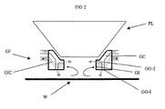
- FIG. 2 represents an embodiment of the gas flushing system GF in more detail.
- Gas flushing system GF comprises a first gas outlet GO-1 and a second gas outlet GO-2.
- GO-1 and GO-2 are connected via gas supply channel GC to a flushing gas supply (not shown) comprising a gas source (not shown) and optionally a flow regulator (not shown).
- a flushing gas supply comprising a gas source (not shown) and optionally a flow regulator (not shown).
- both GO-1 and GO-2 receive gas from a single source.
- GO-1 and GO-2 may also each have a separate gas supply channel, whereby the separate gas supply channels may receive gas from the same source or each may receive gas from a separate gas source.
- At least gas outlet GO-1 receives an oxygen containing gas.
- at least 1 mole% of the gas supplied to GO-1 is oxygen, for instance at least 5 mole%, at least 10 mole %, for instance 10-50 mole% or 10-30 mole%.
- the gas supplied to GO-1 is air.
- GO-2 receives an inert gas, for instance nitrogen, argon, helium, xenon, or mixtures thereof. In other embodiments, both GO-1 and GO-2 receive an inert gas or an oxygen containing gas.
- At least part of the gas exiting GO-1 is directed towards the target portion of substrate W that is being exposed to the radiation exiting the projection system PL (i.e., at least part of the gas exiting GO-1 is directed towards the substrate and angled towards the area being exposed to the radiation). In one embodiment, essentially all gas exiting GO-1 is directed towards the target portion of substrate W that is being exposed to the radiation exiting the projection system PL (only the bottom section of projection system PL is shown).
- the gas flow from outlet GO-1 is adjusted such that, at the used substrate table (or substrate support) velocity, the velocity of the radial gas flow, at every location in the space between the gas flushing system and the substrate is higher than zero and directed inwards, i.e. towards the area between the substrate and the projection system.
- the radial gas flow velocity is the vectorial sum of gas flow speed created at the outlet(s) GO-1 and the substrate table velocity.
- substrate table velocity includes, e.g., the substrate table (or substrate support) scanning velocity of a step-and-scan type lithographic projection apparatus, as well as, in the case of a step-and-repeat type lithographic projection apparatus, the velocity of the wafer table between subsequent exposures.
- gas flushing system GF comprises a gas inlet GI for extracting gas from the space between the target portion being exposed and the projection system.
- Gas inlet GI is connected via channel GIC to a gas extraction system (not shown), which may include a vacuum pump and/or a fan for facilitating the removal of the gas.
- the gas extraction system may include a flow regulator.
- the gas flushing system comprises one or more sensors, e.g. for determining the amount and/or type of harmful gases entering the area between the substrate and the projection system.
- the one or more sensors may be used to adjust the composition and/or rate of the flushing gas, e.g. relative to the amount and/or type of harmful gases entering the area between the substrate and the projection system.
- the one or more sensors may be used to monitor the proper functioning of the gas flushing system and to provide, e.g., a warning if the flow rate through the gas inlet GI is too low.
- gas flushing system GF has a circular construction and, along its inner circumference, only part of the gas flushing system is provided with a gas outlet section GO-2.
- gas outlet ports GO-2 are provided all along the inner circumference of the gas flushing system, and in Figure 3c the gas flushing system GF is provided with opposing gas outlet ports.
- gas outlet port(s) GO-2 provide a laminar flow substantially parallel to the surface of the substrate and/or the surface of the bottom lens of projection system PL.
- the provided is a lithographic projection apparatus comprising:
- a lithographic projection apparatus comprising:
- a lithographic projection apparatus comprising:
- Figure 4 shows an embodiment of a gas flushing system GF having no gas outlet ports but only gas inlet ports GI. Air flow is created by connecting the gas inlet port channels GIC to a gas extraction system (not shown) and using the gas extraction system to suck air from other areas of the lithographic apparatus towards the gas inlet ports GI and through the gas inlet port channels GIC.
- This embodiment may be advantageous, e.g., when the lithographic apparatus design does not allow sufficient space between the wafer stage and last lens element to have both gas supply channels (gas outlets) and gas extraction channels (gas inlets).
- the embodiment of gas flushing system GF in Figure 4 also has openings S 1 and S2 which allow sensor/measurement beams to reach the wafer through the gas flushing system.
- the gas flushing system GF may have a plurality of openings S2, for instance 4 equidistant openings (compare openings S1).
- opening S1 allows access to the wafer for an image sensor (e.g. a reflective image sensor) and S2 allows access for a level sensor.
- the openings are covered with windows, e.g. glass or pellicles.
- openings S 1 are covered with glass.
- openings S2 are covered with pellicles. Covering the openings may be useful, e.g., in preventing gases from exiting the gas flushing system through these openings.
- the gas flushing system is useful in processes where there is a risk of harmful gases evaporating from a substrate during exposure to radiation. Such gases may, for instance, damage the projection system or surrounding parts, which may in turn require increased maintenance and/or shorten the lifetime of the projection system or surrounding parts.
- the gas flushing system of the present invention is helpful in preventing such damage by substantially preventing harmful gases from reaching the projection system or surrounding parts.
- Substrates that are prone to releasing gases are, for instance, substrates coated with one or more resist layers. Particularly, substrates coated with resist layers for one or more colour filter layers may be susceptible to releasing gases. Substrates coated with resist layers for one or more colour filter layers may be used in the manufacturing of image sensors, for instance image sensors useful in cameras (e.g. photo cameras or video cameras).
Landscapes
- Health & Medical Sciences (AREA)
- Epidemiology (AREA)
- Public Health (AREA)
- Physics & Mathematics (AREA)
- General Physics & Mathematics (AREA)
- Life Sciences & Earth Sciences (AREA)
- Atmospheric Sciences (AREA)
- Engineering & Computer Science (AREA)
- Environmental & Geological Engineering (AREA)
- Exposure And Positioning Against Photoresist Photosensitive Materials (AREA)
- Exposure Of Semiconductors, Excluding Electron Or Ion Beam Exposure (AREA)
Applications Claiming Priority (2)
| Application Number | Priority Date | Filing Date | Title |
|---|---|---|---|
| US63372704P | 2004-12-07 | 2004-12-07 | |
| US11/036,186 US20060119811A1 (en) | 2004-12-07 | 2005-01-18 | Radiation exposure apparatus comprising a gas flushing system |
Publications (2)
| Publication Number | Publication Date |
|---|---|
| EP1669809A2 true EP1669809A2 (de) | 2006-06-14 |
| EP1669809A3 EP1669809A3 (de) | 2006-11-29 |
Family
ID=36084297
Family Applications (1)
| Application Number | Title | Priority Date | Filing Date |
|---|---|---|---|
| EP05257485A Ceased EP1669809A3 (de) | 2004-12-07 | 2005-12-06 | Strahlungsbelichtungsgerät mit Gasspülsystem |
Country Status (7)
| Country | Link |
|---|---|
| US (2) | US20060119811A1 (de) |
| EP (1) | EP1669809A3 (de) |
| JP (1) | JP2006186352A (de) |
| KR (1) | KR100749943B1 (de) |
| CN (1) | CN1797220A (de) |
| SG (1) | SG123681A1 (de) |
| TW (1) | TW200628997A (de) |
Families Citing this family (16)
| Publication number | Priority date | Publication date | Assignee | Title |
|---|---|---|---|---|
| KR100727847B1 (ko) * | 2005-09-07 | 2007-06-14 | 세메스 주식회사 | 기판 가장자리 노광 장치 |
| JP4814610B2 (ja) * | 2005-10-25 | 2011-11-16 | 株式会社ニューフレアテクノロジー | 吸引補助具 |
| IL183693A0 (en) * | 2007-06-05 | 2007-09-20 | Nova Measuring Instr Ltd | Optical method and system |
| JP5448724B2 (ja) | 2009-10-29 | 2014-03-19 | キヤノン株式会社 | 露光装置及びデバイスの製造方法 |
| NL2006243A (en) * | 2010-03-19 | 2011-09-20 | Asml Netherlands Bv | A lithographic apparatus, an illumination system, a projection system and a method of manufacturing a device using a lithographic apparatus. |
| CN111352309B (zh) | 2015-04-20 | 2024-03-01 | Asml荷兰有限公司 | 光刻设备和光刻工艺中的方法 |
| US10018920B2 (en) * | 2016-03-04 | 2018-07-10 | Taiwan Semiconductor Manufacturing Co., Ltd. | Lithography patterning with a gas phase resist |
| US11397385B2 (en) | 2016-06-17 | 2022-07-26 | Taiwan Semiconductor Manufacturing Company, Ltd | Apparatus and a method of forming a particle shield |
| US10168626B2 (en) | 2016-06-17 | 2019-01-01 | Taiwan Semiconductor Manufacturing Company, Ltd. | Apparatus and a method of forming a particle shield |
| US10788764B2 (en) * | 2016-06-17 | 2020-09-29 | Taiwan Semiconductor Manufacturing Company, Ltd. | Apparatus and a method of forming a particle shield |
| CN107552258B (zh) | 2016-07-01 | 2019-06-07 | 江苏鲁汶仪器有限公司 | 气体喷射装置 |
| CN109283797B (zh) * | 2017-07-21 | 2021-04-30 | 上海微电子装备(集团)股份有限公司 | 物镜保护装置、物镜系统以及光刻设备 |
| CN115701293B (zh) | 2020-06-04 | 2026-04-24 | Asml荷兰有限公司 | 流体净化系统、投射系统、照射系统、光刻设备和方法 |
| EP3923076A1 (de) * | 2020-06-09 | 2021-12-15 | ASML Netherlands B.V. | Flüssigkeitsspülsystem |
| CN114460814B (zh) * | 2022-01-20 | 2024-04-02 | 中国科学院微电子研究所 | 光刻设备、气浴装置及其气浴发生器 |
| CN115390365B (zh) * | 2022-08-09 | 2025-04-01 | 中国科学院微电子研究所 | 气浴发生器及光刻设备 |
Citations (9)
| Publication number | Priority date | Publication date | Assignee | Title |
|---|---|---|---|---|
| US5229872A (en) | 1992-01-21 | 1993-07-20 | Hughes Aircraft Company | Exposure device including an electrically aligned electronic mask for micropatterning |
| US5296891A (en) | 1990-05-02 | 1994-03-22 | Fraunhofer-Gesellschaft Zur Forderung Der Angewandten Forschung E.V. | Illumination device |
| US5523193A (en) | 1988-05-31 | 1996-06-04 | Texas Instruments Incorporated | Method and apparatus for patterning and imaging member |
| WO1998033096A1 (en) | 1997-01-29 | 1998-07-30 | Micronic Laser Systems Ab | Method and apparatus for the production of a structure by focused laser radiation on a photosensitively coated substrate |
| WO1998038597A2 (en) | 1997-02-28 | 1998-09-03 | Micronic Laser Systems Ab | Data-conversion method for a multibeam laser writer for very complex microlithographic patterns |
| WO1998040791A1 (en) | 1997-03-10 | 1998-09-17 | Koninklijke Philips Electronics N.V. | Positioning device having two object holders |
| US5969441A (en) | 1996-12-24 | 1999-10-19 | Asm Lithography Bv | Two-dimensionally balanced positioning device with two object holders, and lithographic device provided with such a positioning device |
| EP1098226A2 (de) | 1999-11-05 | 2001-05-09 | Asm Lithography B.V. | Lithographischer Apparat mit Spülgassystem |
| US20040212791A1 (en) | 2003-02-12 | 2004-10-28 | Asml Netherlands B.V. | Lithographic apparatus comprising a gas flushing system |
Family Cites Families (23)
| Publication number | Priority date | Publication date | Assignee | Title |
|---|---|---|---|---|
| US5559584A (en) * | 1993-03-08 | 1996-09-24 | Nikon Corporation | Exposure apparatus |
| JP3387075B2 (ja) * | 1994-12-12 | 2003-03-17 | 株式会社ニコン | 走査露光方法、露光装置、及び走査型露光装置 |
| US6771314B1 (en) * | 1998-03-31 | 2004-08-03 | Intel Corporation | Orange-green-blue (OGB) color system for digital image sensor applications |
| JP2000200745A (ja) | 1999-01-07 | 2000-07-18 | Nikon Corp | 投影露光装置 |
| EP1229573A4 (de) * | 1999-07-16 | 2006-11-08 | Nikon Corp | Belichtungsverfahren und -system |
| TW480372B (en) * | 1999-11-05 | 2002-03-21 | Asm Lithography Bv | Lithographic projection apparatus, method of manufacturing a device using the apparatus, and device manufactured according to the method |
| US6933513B2 (en) * | 1999-11-05 | 2005-08-23 | Asml Netherlands B.V. | Gas flushing system for use in lithographic apparatus |
| TW563002B (en) * | 1999-11-05 | 2003-11-21 | Asml Netherlands Bv | Lithographic projection apparatus, method of manufacturing a device using a lithographic projection apparatus, and device manufactured by the method |
| EP1458028B1 (de) * | 1999-12-02 | 2011-05-11 | Nikon Corporation | Festkörperbildsensor und dessen Herstellungsverfahren |
| US6747729B2 (en) * | 2000-07-14 | 2004-06-08 | Asml Netherlands B.V. | Lithographic projection apparatus, device manufacturing method, device manufactured thereby and gas composition |
| US6671396B1 (en) * | 2000-09-18 | 2003-12-30 | Taiwan Semiconductor Manufacturing Company | Method to monitor stepper lens quality in color filter process |
| JP4081813B2 (ja) | 2000-11-10 | 2008-04-30 | 株式会社ニコン | 光学装置、露光装置、及びデバイス製造方法 |
| KR100866818B1 (ko) * | 2000-12-11 | 2008-11-04 | 가부시키가이샤 니콘 | 투영광학계 및 이 투영광학계를 구비한 노광장치 |
| JP2002373852A (ja) * | 2001-06-15 | 2002-12-26 | Canon Inc | 露光装置 |
| US6828569B2 (en) * | 2001-11-19 | 2004-12-07 | Asml Netherlands B.V. | Lithographic projection apparatus, device manufacturing method and device manufactured thereby |
| US20030224265A1 (en) * | 2001-12-11 | 2003-12-04 | Uzodinma Okoroanyanwu | System and method for reducing photoresist photo-oxidative degradation in 193 nm photolithography |
| US6710370B2 (en) * | 2002-01-07 | 2004-03-23 | Xerox Corporation | Image sensor with performance enhancing structures |
| DE10211611A1 (de) | 2002-03-12 | 2003-09-25 | Zeiss Carl Smt Ag | Verfahren und Vorrichtung zur Dekontamination optischer Oberflächen |
| JP4677174B2 (ja) * | 2003-02-03 | 2011-04-27 | キヤノン株式会社 | 位置検出装置 |
| JP4289906B2 (ja) * | 2003-02-28 | 2009-07-01 | キヤノン株式会社 | 露光装置 |
| JP2004080052A (ja) | 2003-11-04 | 2004-03-11 | Canon Inc | 露光装置、デバイスの製造方法 |
| US7136142B2 (en) | 2004-05-25 | 2006-11-14 | Asml Netherlands B.V. | Lithographic apparatus having a gas flushing device |
| US7446850B2 (en) * | 2004-12-03 | 2008-11-04 | Asml Netherlands B.V. | Lithographic apparatus and device manufacturing method |
-
2005
- 2005-01-18 US US11/036,186 patent/US20060119811A1/en not_active Abandoned
- 2005-12-02 SG SG200507762A patent/SG123681A1/en unknown
- 2005-12-05 JP JP2005350407A patent/JP2006186352A/ja active Pending
- 2005-12-05 TW TW094142799A patent/TW200628997A/zh unknown
- 2005-12-05 CN CNA2005101380850A patent/CN1797220A/zh active Pending
- 2005-12-06 EP EP05257485A patent/EP1669809A3/de not_active Ceased
- 2005-12-06 KR KR1020050118097A patent/KR100749943B1/ko not_active Expired - Fee Related
- 2005-12-06 US US11/294,348 patent/US7570342B2/en not_active Expired - Fee Related
Patent Citations (9)
| Publication number | Priority date | Publication date | Assignee | Title |
|---|---|---|---|---|
| US5523193A (en) | 1988-05-31 | 1996-06-04 | Texas Instruments Incorporated | Method and apparatus for patterning and imaging member |
| US5296891A (en) | 1990-05-02 | 1994-03-22 | Fraunhofer-Gesellschaft Zur Forderung Der Angewandten Forschung E.V. | Illumination device |
| US5229872A (en) | 1992-01-21 | 1993-07-20 | Hughes Aircraft Company | Exposure device including an electrically aligned electronic mask for micropatterning |
| US5969441A (en) | 1996-12-24 | 1999-10-19 | Asm Lithography Bv | Two-dimensionally balanced positioning device with two object holders, and lithographic device provided with such a positioning device |
| WO1998033096A1 (en) | 1997-01-29 | 1998-07-30 | Micronic Laser Systems Ab | Method and apparatus for the production of a structure by focused laser radiation on a photosensitively coated substrate |
| WO1998038597A2 (en) | 1997-02-28 | 1998-09-03 | Micronic Laser Systems Ab | Data-conversion method for a multibeam laser writer for very complex microlithographic patterns |
| WO1998040791A1 (en) | 1997-03-10 | 1998-09-17 | Koninklijke Philips Electronics N.V. | Positioning device having two object holders |
| EP1098226A2 (de) | 1999-11-05 | 2001-05-09 | Asm Lithography B.V. | Lithographischer Apparat mit Spülgassystem |
| US20040212791A1 (en) | 2003-02-12 | 2004-10-28 | Asml Netherlands B.V. | Lithographic apparatus comprising a gas flushing system |
Non-Patent Citations (1)
| Title |
|---|
| "MICROCHIP FABRICATION: A PRACTICAL GUIDE TO SEMICONDUCTOR PROCESSING", 1997, MCGRAW HILL PUBLISHING CO. |
Also Published As
| Publication number | Publication date |
|---|---|
| CN1797220A (zh) | 2006-07-05 |
| US20060146300A1 (en) | 2006-07-06 |
| KR20060083853A (ko) | 2006-07-21 |
| SG123681A1 (en) | 2006-07-26 |
| US20060119811A1 (en) | 2006-06-08 |
| US7570342B2 (en) | 2009-08-04 |
| EP1669809A3 (de) | 2006-11-29 |
| KR100749943B1 (ko) | 2007-08-16 |
| JP2006186352A (ja) | 2006-07-13 |
| TW200628997A (en) | 2006-08-16 |
Similar Documents
| Publication | Publication Date | Title |
|---|---|---|
| US7570342B2 (en) | Radiation exposure apparatus comprising a gas flushing system | |
| US7081943B2 (en) | Lithographic apparatus and device manufacturing method | |
| EP1278089A2 (de) | Lithographisches Gerät und zugehöriges Herstellungsverfahren | |
| EP1429189B1 (de) | Lithographischer Apparat und Verfahren zur Herstellung einer Vorrichtung | |
| EP1447716A2 (de) | Lithographischer Apparat mit Spülgassystem | |
| EP1548507A1 (de) | Messverfahren und Substrat | |
| US6956222B2 (en) | Lithographic apparatus and method of manufacturing a device | |
| EP1324136A1 (de) | Lithographischer Projektionsapparat und Verfahren zur Herstellung eines Artikels | |
| US6734949B2 (en) | Lithographic apparatus and device manufacturing method | |
| TWI271601B (en) | Lithographic apparatus and device manufacturing method | |
| EP1469349A1 (de) | Lithographische Projektionsvorrichtung mit einem einen Konkavspiegel und einen Konvexspiegel aufweisenden Kollektor | |
| US6714279B2 (en) | Lithographic projection apparatus, device manufacturing method and device manufactured thereby | |
| EP1394616A1 (de) | Ausrichtgerät, lithographischer Apparat, Ausrichtungsverfahren und Verfahren zur Herstellung einer Vorrichtung | |
| US7088421B2 (en) | Lithographic apparatus, device manufacturing method, and device manufactured thereby | |
| US20050002003A1 (en) | Lithographic apparatus and device manufacturing method | |
| EP1310829A1 (de) | Lithographischer Apparat und Verfahren zur Herstellung einer Vorrichtung | |
| EP1186958B1 (de) | Lithographischer Projektionsapparat | |
| EP1411388A1 (de) | Verfahren zur Reinigung durch Entfernung von Teilchen von Oberflächen, Reinigungsvorrichtung und lithographischer Projektionsapparat | |
| EP1256847B1 (de) | Lithographischer Apparat mit Spülgassystem | |
| EP1324137A2 (de) | Verfahren zur Herstellung eines Artikels, dabei hergestellter Artikel und lithographischer Apparat dafür | |
| EP1434100A2 (de) | Lithographischer Apparat | |
| US7294844B2 (en) | Lithographic apparatus, device manufacturing method, and device manufactured thereby | |
| EP1396759A2 (de) | Lithographischer Apparat, Verfahren zur Herstellung eines Artikels und damit erzeugter Artikel | |
| EP1596421A2 (de) | Lithographischer Apparat und Verfahren zur Herstellung einer Vorrichtung | |
| EP1333329B1 (de) | Lithographischer Apparat und Verfahren zur Herstellung einer Vorrichtung |
Legal Events
| Date | Code | Title | Description |
|---|---|---|---|
| PUAI | Public reference made under article 153(3) epc to a published international application that has entered the european phase |
Free format text: ORIGINAL CODE: 0009012 |
|
| AK | Designated contracting states |
Kind code of ref document: A2 Designated state(s): AT BE BG CH CY CZ DE DK EE ES FI FR GB GR HU IE IS IT LI LT LU LV MC NL PL PT RO SE SI SK TR |
|
| AX | Request for extension of the european patent |
Extension state: AL BA HR MK YU |
|
| PUAL | Search report despatched |
Free format text: ORIGINAL CODE: 0009013 |
|
| AK | Designated contracting states |
Kind code of ref document: A3 Designated state(s): AT BE BG CH CY CZ DE DK EE ES FI FR GB GR HU IE IS IT LI LT LU LV MC NL PL PT RO SE SI SK TR |
|
| AX | Request for extension of the european patent |
Extension state: AL BA HR MK YU |
|
| 17P | Request for examination filed |
Effective date: 20070521 |
|
| 17Q | First examination report despatched |
Effective date: 20070621 |
|
| AKX | Designation fees paid |
Designated state(s): DE FR GB IT NL |
|
| STAA | Information on the status of an ep patent application or granted ep patent |
Free format text: STATUS: THE APPLICATION HAS BEEN REFUSED |
|
| 18R | Application refused |
Effective date: 20081011 |