EP1667248A1 - Organic light emitting device having cathode including a magnesium-calcium layer and method for fabricating the same - Google Patents
Organic light emitting device having cathode including a magnesium-calcium layer and method for fabricating the same Download PDFInfo
- Publication number
- EP1667248A1 EP1667248A1 EP05111200A EP05111200A EP1667248A1 EP 1667248 A1 EP1667248 A1 EP 1667248A1 EP 05111200 A EP05111200 A EP 05111200A EP 05111200 A EP05111200 A EP 05111200A EP 1667248 A1 EP1667248 A1 EP 1667248A1
- Authority
- EP
- European Patent Office
- Prior art keywords
- layer
- cathode
- light emitting
- emitting device
- organic light
- Prior art date
- Legal status (The legal status is an assumption and is not a legal conclusion. Google has not performed a legal analysis and makes no representation as to the accuracy of the status listed.)
- Granted
Links
Images


Classifications
-
- H—ELECTRICITY
- H10—SEMICONDUCTOR DEVICES; ELECTRIC SOLID-STATE DEVICES NOT OTHERWISE PROVIDED FOR
- H10K—ORGANIC ELECTRIC SOLID-STATE DEVICES
- H10K50/00—Organic light-emitting devices
- H10K50/80—Constructional details
- H10K50/805—Electrodes
- H10K50/82—Cathodes
- H10K50/828—Transparent cathodes, e.g. comprising thin metal layers
-
- H—ELECTRICITY
- H05—ELECTRIC TECHNIQUES NOT OTHERWISE PROVIDED FOR
- H05B—ELECTRIC HEATING; ELECTRIC LIGHT SOURCES NOT OTHERWISE PROVIDED FOR; CIRCUIT ARRANGEMENTS FOR ELECTRIC LIGHT SOURCES, IN GENERAL
- H05B33/00—Electroluminescent light sources
- H05B33/12—Light sources with substantially two-dimensional [2D] radiating surfaces
- H05B33/26—Light sources with substantially two-dimensional [2D] radiating surfaces characterised by the composition or arrangement of the conductive material used as an electrode
-
- H—ELECTRICITY
- H05—ELECTRIC TECHNIQUES NOT OTHERWISE PROVIDED FOR
- H05B—ELECTRIC HEATING; ELECTRIC LIGHT SOURCES NOT OTHERWISE PROVIDED FOR; CIRCUIT ARRANGEMENTS FOR ELECTRIC LIGHT SOURCES, IN GENERAL
- H05B33/00—Electroluminescent light sources
- H05B33/10—Apparatus or processes specially adapted to the manufacture of electroluminescent light sources
-
- H—ELECTRICITY
- H10—SEMICONDUCTOR DEVICES; ELECTRIC SOLID-STATE DEVICES NOT OTHERWISE PROVIDED FOR
- H10K—ORGANIC ELECTRIC SOLID-STATE DEVICES
- H10K50/00—Organic light-emitting devices
- H10K50/80—Constructional details
- H10K50/84—Passivation; Containers; Encapsulations
- H10K50/844—Encapsulations
-
- Y—GENERAL TAGGING OF NEW TECHNOLOGICAL DEVELOPMENTS; GENERAL TAGGING OF CROSS-SECTIONAL TECHNOLOGIES SPANNING OVER SEVERAL SECTIONS OF THE IPC; TECHNICAL SUBJECTS COVERED BY FORMER USPC CROSS-REFERENCE ART COLLECTIONS [XRACs] AND DIGESTS
- Y10—TECHNICAL SUBJECTS COVERED BY FORMER USPC
- Y10T—TECHNICAL SUBJECTS COVERED BY FORMER US CLASSIFICATION
- Y10T428/00—Stock material or miscellaneous articles
- Y10T428/24—Structurally defined web or sheet [e.g., overall dimension, etc.]
- Y10T428/24942—Structurally defined web or sheet [e.g., overall dimension, etc.] including components having same physical characteristic in differing degree
-
- Y—GENERAL TAGGING OF NEW TECHNOLOGICAL DEVELOPMENTS; GENERAL TAGGING OF CROSS-SECTIONAL TECHNOLOGIES SPANNING OVER SEVERAL SECTIONS OF THE IPC; TECHNICAL SUBJECTS COVERED BY FORMER USPC CROSS-REFERENCE ART COLLECTIONS [XRACs] AND DIGESTS
- Y10—TECHNICAL SUBJECTS COVERED BY FORMER USPC
- Y10T—TECHNICAL SUBJECTS COVERED BY FORMER US CLASSIFICATION
- Y10T428/00—Stock material or miscellaneous articles
- Y10T428/26—Web or sheet containing structurally defined element or component, the element or component having a specified physical dimension
Definitions
- the present invention relates to an organic light emitting device having a cathode including a magnesium-calcium layer and a method for fabricating the same.
- an organic light emitting device includes an anode, an organic emission layer disposed on the anode, and a cathode disposed on the organic emission layer.
- a voltage is applied between the anode and the cathode, holes are injected into the organic emission layer from the anode and electrons are injected into the organic emission layer from the cathode.
- the holes and electrons that are injected into the organic emission layer are combined in the organic emission layer to create excitons, and the excitons are transitioned from an excited state to a ground state to emit light.
- the cathode should have a low work function in order to readily inject the electrons into the organic emission layer.
- a material that satisfies this condition is magnesium that has a work function of 3.46 eV.
- the magnesium cannot be used to form a stable organic light emitting device since it reacts with external oxygen or moisture.
- U.S. Patent No. 4,885,211 uses a cathode having high ambient stability by forming the cathode with a magnesium-silver (Mg-Ag) alloy.
- Mg-Ag magnesium-silver
- the magnesium-silver alloy cathode may have inferior electron injection characteristics compared to the magnesium cathode.
- a lithium fluoride (LiF) layer is deposited onto an electron transport layer (Alq) and an Mg-Ag layer is deposited onto the LiF layer, thereby forming a bilayer cathode of LiF/Mg-Ag.
- the bilayer cathode of LiF/Mg-Ag may have improved electron injection characteristics when compared to a single layer cathode comprising Mg-Ag.
- the manufacturing cost may increase and throughput may be reduced.
- the present invention provides an organic light emitting device with a cathode that has improved electron injection characteristics without requiring a separate electron injection layer.
- the present invention discloses an organic light emitting device including an anode and a cathode including a magnesium-calcium layer.
- An organic layer including at least an organic emission layer is interposed between the anode and the cathode.
- the cathode comprises magnesium and calcium in an atomic ratio of about 1:(1/3) to about 1:3.
- the cathode comprises magnesium and calcium in an atomic ratio of about 1:1.
- the organic light emitting device further comprises a capping layer in contact with a surface of the cathode opposite a surface of the cathode that is in contact with the organic layer.
- the capping layer is selected from the group consisting of an organic layer, an inorganic layer, and a multilayer of the organic layer and the inorganic layer.
- the inorganic layer is selected from the group consisting of a silicon oxide (SiO 2 ) layer, a silicon nitride (SiNx) layer, and a silicon oxynitride (SiOxNy) layer.
- the inorganic layer is selected from the group consisting of an indium tin oxide (ITO) layer, an indium zinc oxide (IZO) layer, a tin oxide (TN) layer, and a zinc oxide (ZnO) layer.
- the inorganic layer is a lithium fluoride (LiF) layer.
- the organic layer comprises at least one selected from the group consisting of NPB, TNATA, TCTA, TDAPB, TDATA, Alq3, Balq and CBP.
- the organic layer further comprises an electron transport layer interposed between the cathode and the organic emission layer, and wherein the electron transport layer contacts the cathode.
- the organic layer further comprises at least one of a hole injection layer and a hole transport layer interposed between the anode and the organic emission layer.
- the present invention further discloses an organic light emitting device comprising an anode, a light transmissive cathode of a magnesium-calcium layer, and an organic layer interposed between the anode and the cathode and having at least an organic emission layer.
- the light transmissive cathode comprises magnesium and calcium in an atomic ratio of about 1:(1/3) to about 1:3.
- the light transmissive cathode comprises magnesium and calcium in an atomic ratio of about 1:1.
- the light transmissive cathode is about 400 ⁇ or less thick. In another preferred embodiment the light transmissive cathode is about 100 ⁇ or more thick. In another preferred embodiment the light transmissive cathode is about 200 ⁇ to about 300 ⁇ thick.
- the organic light emitting device further comprises a capping layer that is in contact with a surface of the light transmissive cathode opposite a surface of the light transmissive cathode in contact with the organic layer.
- the capping layer is a transparent capping layer.
- the capping layer has a refractive index that is larger than that of the cathode.
- the capping layer has a refractive index of about 1.3 to about 2.3.
- the capping layer is selected from the group consisting of an organic layer, an inorganic layer, and a multilayer of the organic layer and the inorganic layer.
- the present invention also discloses a method for fabricating an organic light emitting device comprising forming an anode on a substrate, forming an organic layer comprising at least an organic emission layer on the anode, and forming a cathode comprising a magnesium-calcium layer on the organic layer.
- the cathode is formed by co-depositing magnesium and calcium in an atomic ratio of about 1:(1/3) to about 1:3.
- the cathode is formed by co-depositing magnesium and calcium in an atomic ratio of about 1:1.
- the cathode is about 100 ⁇ to about 400 ⁇ thick.
- the method further comprises forming a capping layer on the cathode.
- the capping layer is formed of one selected from the group consisting of an organic layer, an inorganic layer, and a multilayer of the organic layer and the inorganic layer.
- FIG. 1 is a cross-sectional view of an organic light emitting device according to an exemplary embodiment of the present invention.
- FIG. 2 is a graph of accelerated lifespan characteristics of red organic light emitting devices according to a first example and a first comparative example.
- FIG. 3 is a graph of accelerated lifespan characteristics of green organic light emitting devices according to a second example and second and third comparative examples.
- FIG. 4A is a graph of accelerated lifespan characteristics of blue organic light emitting devices according to a fifth example and fourth and fifth comparative examples.
- FIG. 4B is a graph of accelerated lifespan characteristics of blue organic light emitting devices according to third to sixth examples and a fifth comparative example.
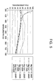
- FIG. 5 is a graph of transmissivity versus wavelength of a magnesium-calcium layer and a bilayer of a magnesium-calcium layer/a capping layer according to Example 10, Example 11, Example 12, Example 13 and Example 14.
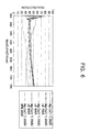
- FIG. 6 is a graph of reflectivity versus wavelength of a magnesium-calcium layer and a bilayer of a magnesium-calcium layer/a capping layer according to Example 10, Example 11, Example 12, Example 13, and Example 14.
- the present invention relates to an organic light emitting device that achieves a reduced driving voltage, increased luminous efficiency, and improved lifespan characteristics without forming a separate electron injection layer. Instead, it uses a cathode comprising an Mg-Ca layer. Improved lifespan characteristics may mean that the cathode of the Mg-Ca layer has high stability against external moisture and oxygen.
- FIG. 1 is a cross-sectional view of an organic light emitting device according to an exemplary embodiment of the present invention.
- an anode 110 is disposed on a substrate 100.
- the substrate 100 may include at least one thin film transistor (not shown) that is coupled with the anode 110.
- the anode 110 may be a transparent electrode or a reflective electrode.
- the anode 110 may be an Indium Tin Oxide (ITO) layer, an Indium Zinc Oxide (IZO) layer, a Tin Oxide (TO) layer, or a Zinc Oxide (ZnO) layer.
- the anode 110 may be a silver (Ag) layer, an aluminum (Al) layer, a nickel (Ni) layer, a platinum (Pt) layer, a palladium (Pd) layer or an alloy layer.
- the anode 110 may also be a transmissive oxide layer such as ITO, IZO, TO, and ZnO that are deposited on the alloy layer.
- the anode 110 may be formed by a vapor phase deposition method such as sputtering and evaporation, ion beam deposition, electron beam deposition, or laser ablation.
- a hole injection layer (HIL) 120 or a hole transport layer (HTL) 130 may be placed on the anode 110.
- the hole injection layer 120 facilitates injection of holes into an emission layer that will be described later.
- the hole injection layer 120 may be formed using a low molecular material such as copper phthalocyanine (CuPc), TNATA, TCTA, TDAPB and TDATA, or a polymer material such as polyaniline (PANI), and poly(3,4)-etyhylenedioxythiophene (PEDOT).
- the hole transport layer 130 facilitates transportation of the holes to the emission layer , which may be formed using a low molecular weight material such as ⁇ -NPB(N,N'-Bis(naphthalene-1-yl)-N,N'-bis(phenyl)benzidine), TPD(N,N'-Bis-(3-methylphenyl)-N,N'-bis-(phenyl)-benzidine), s-TAD and MTDATA(4,4',4"-Tris(N-3-methylphenyl-N-phenyl-amino)-triphenylamine), or a polymer material such as PVK.
- the hole injection layer 120 and the hole transport layer 130 may be formed by vapor deposition, spin coating, inkjet printing, or laser induced thermal imaging.
- An organic emission layer 140 may be disposed on the hole transport layer 130.
- the organic emission layer 140 may be a phosphorescent emission layer or a fluorescent emission layer.
- the organic emission layer 140 may include distyrylarylene (DSA), distyrylarylene derivative, distrylbenzene (DSB), distrylbenzene derivative, DPVBi(4,4'-bis(2,2'-diphenyl vinyl)-1,1'-biphenyl), DPVBi derivative, Spiro-DPVBi, and Spiro-sexyphenyl, for example.
- the organic emission layer 140 may further include a dopant including styrylamine-based, pherylene-based, and distyrylbiphenyl (DSBP)-based materials.
- the organic emission layer 140 when the organic emission layer 140 is the phosphorescent emission layer, the organic emission layer 140 may include, but is not limited to arylamine-based, carbazole-based and Spiro-based materials as a host material.
- the host material may include CBP (4,4-N,N dicarbazole-biphenyl), a CBP derivative, mCP (N,N-dicarbazolyl-3,5-benzene), an mCP derivative, and a Spiro-based derivative.
- the organic emission layer 140 may include a phosphorescent organic metal complex with one central metal including Ir, Pt, Tb and Eu as a dopant material. Further, the phosphorescent organic metal complex may include PQIr, PQIr(acac), PQ 2 Ir(acac), PIQIr(acac) and PtOEP.
- the organic emission layer 140 may be formed by vacuum deposition using a high-resolution mask such as a fine metal mask, inkjet printing, or laser induced thermal imaging.
- a high-resolution mask such as a fine metal mask, inkjet printing, or laser induced thermal imaging.
- a hole blocking layer (HBL) 150 may be disposed on the organic emission layer 140. However, the hole blocking layer 150 may be omitted when the organic emission layer 140 is the fluorescent emission layer. The hole blocking layer 150 suppresses diffusion of excitons created in the organic emission layer 140 when driving the organic light emitting device.
- the hole blocking layer 150 may comprise Balq, BCP, CF-X, TAZ or Spiro-TAZ.
- An electron transport layer (ETL) 160 and an electron injection layer (EIL) 170 may be disposed on the hole blocking layer 150.
- the electron transport layer 160 facilitates the transport of electrons into the organic emission layer 140.
- the electron transport layer 160 may comprise a polymer material such as PBD, TAZ and Spiro-PBD, or a low molecular weight material such as Alq3, Balq and Salq.
- the electron injection layer 170 facilitates the injection of electrons into the organic emission layer 140.
- the electron injection layer 170 may comprise Alq3(tris(8-quinolinolato)aluminum), LiF (lithium fluoride), Ga complex, or PBD. However, the electron injection layer 170 may be omitted. Meanwhile, the electron transport layer 160 and the electron injection layer 170 may be formed by vacuum deposition, spin coating, inkjet printing, or laser induced thermal imaging.
- the hole injection layer 120, the hole transport layer 130, the organic emission layer 140, the hole blocking layer 150, the electron transport layer 160, and the electron injection layer 170 comprise an organic layer A.
- a cathode 180 including a magnesium-calcium (Mg-Ca) layer is disposed on the electron injection layer 170.
- the organic layer A including the organic emission layer 140 is interposed between the anode 110 and the cathode 180. Since the cathode 180 comprising magnesium-calcium has excellent electron injection characteristics, the organic light emitting device including the magnesium-calcium layer has low driving voltage characteristics and high luminous efficiency characteristics even when the electron injection layer 170 is not formed, i.e., the cathode 180 and the electron transport layer 160 are in contact with each other. Therefore, the manufacturing cost may be reduced and the throughput in manufacturing the organic light emitting device may be increased.
- Mg-Ca magnesium-calcium
- the cathode 180 includes Mg and Ca in an atomic ratio of about 1:(1/3) to about 1:3.
- the cathode 180 may comprise Mg and Ca in an atomic ratio of about 1:1.
- the cathode 180 has an appropriate sheet resistance. Therefore, when the organic light emitting device is operated, a voltage (IR) drop due to the sheet resistance of the cathode 180 may be suppressed.
- the cathode 180 may be a light transmissive cathode.
- the cathode 180 may be about 400 ⁇ or less thick to allow for light transmittance. Further, the cathode 180 may be about 100 ⁇ thick considering forming a layer with uniformity and sheet resistance. In general, the cathode 180 may be about 200 ⁇ to about 300 ⁇ thick.
- a capping layer 190 may be disposed on the cathode 180 on a surface opposite a surface adjacent to the organic layer A.
- the capping layer 190 may be an organic layer, an inorganic layer, or a multilayer of the organic layer and the inorganic layer.
- the inorganic layer may be a silicon oxide (SiO 2 ) layer, a silicon nitride (SiN x ) layer, or a silicon oxynitride (SiO x N y ) layer, which is an insulating layer.
- the inorganic layer may be an ITO layer, an IZO layer, a TO layer, or a ZnO layer which is a transparent conductive layer.
- the inorganic layer may be a LiF layer.
- the organic layer may comprise NPB(N,N'-Bis(naphthalene-1-yl)-N,N'-bis(phenyl)benzidine), TNATA, TCTA, TDAPB, TDATA, Alq3, Balq, or CBP.
- the capping layer 190 may be formed by evaporation or sputtering. The capping layer 190 protects the organic layer A from external moisture or oxygen to prevent deterioration of the device.
- the capping layer 190 may be a transparent capping layer.
- the capping layer 190 has a higher refractive index than the cathode 180.
- the refractive index of the capping layer 190 may be about 1.3 to about 2.3.
- An anode having an area of 2 mm x 2 mm was formed on a substrate comprising ITO, and was ultrasonically cleaned and UV-O 3 treated.
- 4,4',4"-Tris(N,N-diphenyl-amino)-triphenylamine (TDATA) was vacuum deposited on the UV-O 3 treated anode to a thickness of about 300 ⁇ to form a hole injection layer.
- TDATA 4,4',4"-Tris(N,N-diphenyl-amino)-triphenylamine
- TDATA 4,4',4"-Tris(N,N-diphenyl-amino)-triphenylamine
- TDATA 4,4',4"-Tris(N,N-diphenyl-amino)-triphenylamine
- TDATA 4,4',4"-Tris(N,N-diphenyl-amino)-triphenylamine
- TDATA 4,4',4"-Tris(N,N-diphenyl
- CBP 100 part and PQ 3 Ir 14 part were co-deposited on the hole transport layer to form a 400 ⁇ thick red emission layer.
- Balq3 was deposited on the emission layer to a thickness of about 50 ⁇
- Alq3 was vacuum deposited thereon to a thickness of about 250 ⁇ to form an electron transport layer.
- Mg and Ca were co-deposited on the electron transport layer to form 200 ⁇ thick Mg-Ca layer with an atomic ratio of 1:1, thereby forming a cathode. As a result, a red organic light emitting device was formed.
- the brightness of the organic light emitting device was measured using a photometer.
- the organic light emitting device had a driving voltage of about 5.5 V when the brightness is about 600 cd/m 2 .
- the luminous efficiency was about 8.87 cd/A.
- the decrease in brightness was recorded as a function of time as shown in FIG. 2.
- the initial brightness is about 5 times the brightness (600 cd/m 2 ) that is measured at the driving voltage. Generally, if the initial brightness is 100%, the lifespan is measured as time passes until the brightness is decreased to 50% of the initial brightness.
- Color coordinates of the organic light emitting device were measured using a color analyzer. As a result, color coordinates of (0.676, 0.322) were obtained.
- the organic light emitting device was fabricated by the same method as Example 1 except that Mg and Ag are co-deposited to form a 100 ⁇ thick Mg-Ag layer with an atomic ratio of 10:1, thereby forming a cathode.
- the characteristics were measured by the same method as Example 1. As a result, the driving voltage was about 6.2 V, the brightness was 600 cd/m 2 , luminous efficiency was 7.8 cd/A, color coordinates were (0.687, 0.312), and accelerated lifespan characteristics are shown in FIG. 2.
- Example 1 The characteristics of the red organic light emitting device according to Example 1 and Comparative Example 1 are shown in Table 1, and the accelerated lifespan characteristics are shown in FIG. 2.
- Table 1 Conditions Driving voltage (V) Brightness (cd/m 2 ) Luminous efficiency (cd/A) Color coordinates (CIE_x, CIE_y) EIL Cathode Example 1 - Mg:Ca(1:1), 200 ⁇ 5.5 600 8.87 (0.676, 0.322) Comparative Example 1 - Mg:Ag(10:1 ), 100 ⁇ 6.2 600 7.8 (0.687, 0.312)
- the organic light emitting device of Example 1 had a decreased driving voltage, an increased luminous efficiency, and an increased lifespan when compared to Comparative Example 1.
- the color coordinates had no significant difference. Therefore, the organic light emitting device using the Mg-Ca layer as a cathode has improved driving voltage characteristics, luminous efficiency characteristics, and lifespan characteristics when compared with the organic light emitting device using the Mg-Ag layer as a cathode. Characteristics of a green organic light emitting device including a cathode of an Mg-Ca layer
- An anode having an area of 2 mm x 2 mm was formed on a substrate comprising ITO, and was ultrasonically cleaned and UV-O 3 treated.
- 4,4',4"-Tris(N,N-diphenyl-amino)-triphenylamine (TDATA) was vacuum deposited on the UV-O 3 treated anode to a thickness of about 200 ⁇ to form a hole injection layer.
- TDATA 4,4',4"-Tris(N,N-diphenyl-amino)-triphenylamine
- TDATA 4,4',4"-Tris(N,N-diphenyl-amino)-triphenylamine
- TDATA 4,4',4"-Tris(N,N-diphenyl-amino)-triphenylamine
- TDATA 4,4',4"-Tris(N,N-diphenyl-amino)-triphenylamine
- TDATA 4,4',4"-Tris(N,N-diphenyl
- CBP 100 part and Ir(ppy) 3 6 part were co-deposited on the hole transport layer to form a 400 ⁇ thick green emission layer.
- Balq3 was deposited on the emission layer to a thickness of about 50 ⁇
- Alq3 was vacuum deposited thereon to a thickness of about 250 ⁇ to form an electron transport layer.
- Mg and Ca were co-deposited on the electron transport layer to form 200 ⁇ thick Mg-Ca layer with an atomic ratio of 1:1, thereby forming a cathode. As a result, a green organic light emitting device was formed.
- the brightness of the organic light emitting device was measured using a photometer.
- the organic light emitting device had a driving voltage of about 4.3 V when the brightness was about 1300 cd/m 2 .
- the luminous efficiency was about 66 cd/A.
- the decrease in brightness was recorded as a function of time, as shown in FIG. 3.
- the initial brightness was about 5 times the brightness (1300 cd/m 2 ) that was measured at the driving voltage.
- Color coordinates of the organic light emitting device were measured using a color analyzer. As a result, color coordinates of (0.303, 0.649) were obtained.
- the organic light emitting device was fabricated by the same method as Example 2 except that Mg and Ag were co-deposited to form a 100 ⁇ thick Mg-Ag layer with an atomic ratio of 10:1, thereby forming a cathode.
- the characteristics were measured by the same method as Example 2. As a result, the driving voltage was about 5.2 V, the brightness was 1300 cd/m 2 , luminous efficiency was 55 cd/A, color coordinates were (0.275, 0.678), and accelerated lifespan characteristics are shown in FIG. 3.
- the organic light emitting device was prepared by the same method as Example 2 except that 10 ⁇ thick LiF was vacuum deposited on the electron transport layer to form an electron injection layer (EIL) and 100 ⁇ thick Mg and Ag were co-deposited on the electron injection layer to form an Mg-Ag layer with an atomic ratio of 10:1, thereby forming a cathode.
- EIL electron injection layer
- the characteristics were measured by the same method as Example 2. As a result, the driving voltage was about 4.2 V, brightness was about 1300 cd/m 2 , luminous efficiency was 66 cd/A, color coordinates were (0.264, 0.683), and accelerated lifespan characteristics are shown in FIG. 3.
- Example 2 The characteristics of the green organic light emitting device of Example 2, Comparative Example 2, and Comparative Example 3 are shown in Table 2, and the accelerated lifespan characteristics are shown in FIG. 3.
- the organic light emitting device of Example 2 had a decreased driving voltage, an increased luminous efficiency, and an increased lifespan when compared to Comparative Example 2.
- the color coordinates characteristics were decreased slightly. Therefore, the green organic light emitting device using the Mg-Ca layer as a cathode has improved driving voltage characteristics, luminous efficiency characteristics, and lifespan characteristics when compared with the green organic light emitting device that uses the Mg-Ag layer as a cathode.
- the organic light emitting device of Example 2 had no significant difference in driving voltage, luminous efficiency, and lifespan when compared to Comparative Example 3. Therefore, the organic light emitting device that uses the Mg-Ca layer as a cathode has characteristics that are substantially equal to the organic light emitting device using the Mg-Ag layer as a cathode and using LiF as an electron injection layer. Thus, when the Mg-Ca layer is used as a cathode, the electron injection layer may be omitted. Characteristics of a blue organic light emitting device including a cathode of an Mg-Ca layer
- An anode having an area of 2 mm x 2 mm was formed on a substrate comprising ITO, and was ultrasonically cleaned and UV-O 3 treated.
- 4,4',4"-Tris(N,N-diphenyl-amino)-triphenylamine (TDATA) was vacuum deposited on the UV-O 3 treated anode to a thickness of about 200 ⁇ to form a hole injection layer.
- TDATA 4,4',4"-Tris(N,N-diphenyl-amino)-triphenylamine
- TDATA 4,4',4"-Tris(N,N-diphenyl-amino)-triphenylamine
- TDATA 4,4',4"-Tris(N,N-diphenyl-amino)-triphenylamine
- TDATA 4,4',4"-Tris(N,N-diphenyl-amino)-triphenylamine
- TDATA 4,4',4"-Tris(N,N-diphenyl
- DPVBi was vacuum deposited on the hole transport layer to form a 150 ⁇ thick blue emission layer.
- Alq3 was vacuum deposited on the emission layer to a thickness of about 250 ⁇ , to form an electron transport layer.
- Mg and Ca were co-deposited on the electron transport layer to form a 160 ⁇ thick Mg-Ca layer with an atomic ratio of 1:1, thereby forming a cathode. As a result, a blue organic light emitting device was formed.
- the brightness of the organic light emitting device was measured using a photometer.
- the organic light emitting device had a driving voltage of about 5.0 V when the brightness was about 452 cd/m 2 .
- the luminous efficiency was about 5.07 cd/A.
- the decrease in brightness was recorded as a function of time, as shown in FIG. 4B.
- the initial brightness was about 5 times the brightness (452 cd/m 2 ) that was measured at the driving voltage.
- Color coordinates of the organic light emitting device were measured using a color analyzer. As a result, color coordinates of (0.139, 0.135) were obtained.
- the organic light emitting device was fabricated by the same method as Example 3 except that Mg and Ca were co-deposited to form 180 ⁇ thick Mg-Ca layer with an atomic ratio of 1:1, thereby forming a cathode.
- the organic light emitting device was fabricated by the same method as Example 3 except that Mg and Ca were co-deposited to form a 200 ⁇ thick Mg-Ca layer with an atomic ratio of 1:1, thereby forming a cathode.
- the organic light emitting device was fabricated by the same method as Example 3 except that Mg and Ca were co-deposited to form a 220 ⁇ thick Mg-Ca layer with an atomic ratio of 1:1, thereby forming a cathode.
- the organic light emitting device was fabricated by the same method as Example 3 except that Mg and Ag were co-deposited to form a 100 ⁇ thick Mg-Ag layer with an atomic ratio of 10:1, thereby forming a cathode.
- the characteristics were measured by the same method as Example 3. As a result, driving voltage was about 5.2V, brightness was about 300 cd/m 2 , luminous efficiency was about 1.7 cd/A, color coordinates were (0.140, 0.100), and accelerated lifespan characteristics are shown in FIG. 4A.
- the organic light emitting device was fabricated by the same method as Example 3 except that LiF was vacuum deposited on the electron transport layer to a thickness of 10 ⁇ to from an electron injection layer, and Mg and Ag were co-deposited on the electron injection layer to form a 100 ⁇ thick Mg-Ag layer having an atomic ratio of 10:1, thereby forming a cathode.
- Example 3 The characteristics of the blue organic light emitting device of Example 3, Example 4, Example 5, Example 6, Comparative Example 4, and Comparative Example 5 are shown in Table 3, and the accelerated lifespan characteristics are shown in FIG. 4A and FIG. 4B.
- Table 3 Conditions Driving voltage (V) Brightness (cd/m 2 ) Luminous efficiency (cd/A) Color coordinates (CIE_x, CIE_y) EIL Cathode
- Example 3 Mg:Ca(1:1), 160 ⁇ 5.0 452 5.07 (0.139, 0.135)
- Example 4 Mg:Ca(1:1), 180 ⁇ 4.9 440 4.81 (0.138, 0.132)
- Example 5 Mg:Ca(1:1), 200 ⁇ 4.9 460 5.19 (0.137, 0.137)
- Example 6 Mg:Ca(1:1), 220 ⁇ 4.9 464 5.26 (0.137, 0.138) Comparative Example 4 - Mg:Ag(10:1), 100 ⁇ 5.2 300 1.70 (0.140,
- the organic light emitting devices of Example 3, Example 4, Example 5, and Example 6 had a decreased driving voltage, an increased luminous efficiency, and an increased lifespan when compared to Comparative Example 4, however, the color coordinates characteristics were decreased slightly. Therefore, the blue organic light emitting device using the Mg-Ca layer as a cathode has improved driving voltage characteristics, luminous efficiency characteristics, and lifespan characteristics when compared to the blue organic light emitting device using the Mg-Ag layer as a cathode. In particular, there was no significant difference in driving voltage, luminous efficiency, lifespan and color coordinates characteristics depending on the thickness of the Mg-Ca layers. Therefore, when the Mg-Ca layer is used as a cathode, characteristic uniformity may be obtained even when the case of the large-sized organic light emitting device since there is no characteristic changes depending on thickness deviation.
- the organic light emitting devices of Example 3, Example 4, Example 5, and Example 6 had no significant difference in driving voltage, luminous efficiency and lifespan characteristics when compared to Comparative Example 5. Therefore, the organic light emitting device using the Mg-Ca layer as a cathode has characteristics that are substantially equal to the organic light emitting device using the Mg-Ag layer as a cathode and using LiF as an electron injection layer. Thus, when the Mg-Ca layer is used as a cathode, the electron injection layer may be omitted. Sheet resistance of an Mg-Ca layer
- Mg and Ca had an atomic ratio of 1:(1/3)
- Mg and Ca were co-deposited on a substrate to form a 200 ⁇ thick Mg-Ca layer with an atomic ratio of about 3:1.
- the formed Mg-Ca layer had a sheet resistance of about 60 ⁇ /m 2 .
- an Mg-Ca layer was formed by the same method as Example 7 except that Mg and Ca had an atomic ratio of about 1:1.
- the formed Mg-Ca layer had a sheet resistance of about 16 ⁇ /m 2 .
- an Mg-Ca layer was formed by the same method as Example 7 except that Mg and Ca had an atomic ratio of about 1:3.
- the formed Mg-Ca layer had a sheet resistance of about 48 ⁇ /m 2 .
- Mg and Ag were co-deposited on a substrate to form a 100 ⁇ thick Mg-Ag layer with an atomic ratio of about 10:1.
- the formed Mg-Ag layer had a sheet resistance of about 23 ⁇ /m 2 .
- Sheet resistances of the Mg-Ca layers of Example 7, Example 8, and Example 9 and the Mg-Ag layer of Comparative Example 6 are shown in Table 4.
- Table 4 Conditions Sheet resistance ( ⁇ /m 2 ) Cathode composition (Atomic ratio) Thickness ( ⁇ )
- Example 7 Mg:Ca(3:1) 200 60
- Example 8 Mg:Ca(1:1) 200 16
- Example 9 Mg:Ca (1:3) 200 48 Comparative Example 6 Mg:Ag (10:1) 100 23
- the Mg-Ca layer has a sheet resistance of about 60 ⁇ /m 2 or less.
- the cathode of the organic light emitting device may have a sheet resistance of about 60 ⁇ /m 2 or less. Therefore, the cathode includes Mg and Ca in an atomic ratio of about 1:(1/3) to about 1:3.
- the Mg-Ca layer has the lowest sheet resistance.
- the sheet resistance (16 ⁇ /m 2 ) of the Mg-Ca layer is decreased by about 70% when compared to the sheet resistance (23 ⁇ /m 2 ) of the Mg-Ag layer.
- Mg and Ca were co-deposited on a substrate to form a 200 ⁇ thick Mg-Ca layer with an atomic ratio of 1:1. Then transmissivity and reflectivity of the formed Mg-Ca layer were measured while varying a light wavelength. Results of measurement are shown in FIG. 5 and FIG. 6. At a light wavelength of 550 nm, the transmissivity was 16.82%, and the reflectivity was 31.17%.
- Mg and Ca were co-deposited on a substrate to form a 200 ⁇ thick Mg-Ca layer having an atomic ratio of 1:1, LiF was vacuum deposited on the Mg-Ca layer to a thickness of 700 ⁇ to form a capping layer, and then transmissivity and reflectivity of the Mg-Ca layer and the capping layer were measured while varying a light wavelength. Results of measurement are shown in FIG. 5 and FIG. 6. At a light wavelength of 550 nm, the transmissivity was 48.70%, and the reflectivity was 39.76%.
- An Mg-Ca layer and a capping layer were formed by the same method as Example 11 except that LiF was vacuum deposited on the Mg-Ca layer to a thickness of 800 ⁇ to form the capping layer, and then transmissivity and reflectivity were measured while varying a light wavelength. Results of measurement are shown in FIG. 5 and FIG. 6. At a light wavelength of 550 nm, the transmissivity was 50.48%, and the reflectivity was 42.93%.
- An Mg-Ca layer and a capping layer were formed by the same method as Example 11 except that LiF was vacuum deposited on the Mg-Ca layer to a thickness of 900 ⁇ to form the capping layer, and then transmissivity and reflectivity were measured while varying a light wavelength. Results of measurement are shown in FIG. 5 and FIG. 6. At a light wavelength of 550 nm, the transmissivity was 49.27%, and the reflectivity was 43.50%.
- An Mg-Ca layer and a capping layer were formed by the same method as Example 11 except that NPB was vacuum deposited on the Mg-Ca layer to a thickness of about 600 ⁇ to form the capping layer. Then transmissivity and reflectivity were measured while varying a light wavelength. Results of measurement are shown in FIG. 5 and FIG. 6. At a light wavelength of 550 nm, the transmissivity was 67.31%, and the reflectivity was 37.63%.
- Transmissivity and reflectivity of the Mg-Ca layer at 550 nm and the double layer of the Mg-Ca layer /capping layer of Examples 10, Example 11, Example 12, Example 13, and Example14 are shown in Table 5, and variations of the transmissivity and reflectivity according to a wavelength are shown in FIG. 5 and FIG. 6.
- Example 10 Mg:Ca (1:1), 200 ⁇ - 16.82 31.17
- Example 11 Mg:Ca (1:1), 200 ⁇ LiF, 700 ⁇ 48.70 39.76
- Example 12 Mg:Ca (1:1), 200 ⁇ LiF, 800 ⁇ 50.48 42.93
- Example 13 Mg:Ca (1:1), 200 ⁇ LiF, 900 ⁇ 49.27 43.50
- Example 14 Mg:Ca (1:1), 200 ⁇ NPB, 600 ⁇ 68.31 37.63
- the transmissivity of the double layer of the Mg-Ca layer/the capping layer according to Example 11, Example 12, Example 13, and Example 14 increase when compared to the Mg-Ca layer of Example 10. It is presumed that total reflection of light at a layer interface decreases when the light is transmitted through the double layer of the Mg-Ca layer/the capping layer when compared to when the light is transmitted through only the Mg-Ca layer.
- the capping layer is the LiF layer (Example 11, Example 12, and Example 13)
- variations of the transmissivity based on an increase in thickness of the capping layer are not large.
- the transmissivity is larger when the capping layer is the NPB layer as an organic layer (Example 14) in comparison with when the capping layer is the LiF layer (Example 11, Example 12, and Example 13).
Landscapes
- Physics & Mathematics (AREA)
- Optics & Photonics (AREA)
- Engineering & Computer Science (AREA)
- Manufacturing & Machinery (AREA)
- Electroluminescent Light Sources (AREA)
- Physical Vapour Deposition (AREA)
Abstract
Description
- This application claims priority to and the benefit of Korean Patent Application No. 10-2004-0101428, filed December 3, 2004, the disclosure of which is incorporated herein by reference in its entirety.
- The present invention relates to an organic light emitting device having a cathode including a magnesium-calcium layer and a method for fabricating the same.
- In general, an organic light emitting device includes an anode, an organic emission layer disposed on the anode, and a cathode disposed on the organic emission layer. When a voltage is applied between the anode and the cathode, holes are injected into the organic emission layer from the anode and electrons are injected into the organic emission layer from the cathode. The holes and electrons that are injected into the organic emission layer are combined in the organic emission layer to create excitons, and the excitons are transitioned from an excited state to a ground state to emit light.
- Here, the cathode should have a low work function in order to readily inject the electrons into the organic emission layer. A material that satisfies this condition is magnesium that has a work function of 3.46 eV. However, the magnesium cannot be used to form a stable organic light emitting device since it reacts with external oxygen or moisture.
- In order to solve this problem, U.S. Patent No. 4,885,211 uses a cathode having high ambient stability by forming the cathode with a magnesium-silver (Mg-Ag) alloy. As a result, it is possible to obtain an organic light emitting device with good lifespan characteristics. However, since Ag has a relatively high work function of about 4.28 eV, the magnesium-silver alloy cathode may have inferior electron injection characteristics compared to the magnesium cathode.
- In U.S. Patent No. 5,776,622 a lithium fluoride (LiF) layer is deposited onto an electron transport layer (Alq) and an Mg-Ag layer is deposited onto the LiF layer, thereby forming a bilayer cathode of LiF/Mg-Ag. The bilayer cathode of LiF/Mg-Ag may have improved electron injection characteristics when compared to a single layer cathode comprising Mg-Ag.
- However, when a separate layer is formed to improve the electron injection characteristics of the cathode, the manufacturing cost may increase and throughput may be reduced.
- The present invention provides an organic light emitting device with a cathode that has improved electron injection characteristics without requiring a separate electron injection layer.
- Additional features of the invention will be set forth in the description which follows, and in part will be apparent from the description, or may be learned by practice of the invention.
- The present invention discloses an organic light emitting device including an anode and a cathode including a magnesium-calcium layer. An organic layer including at least an organic emission layer is interposed between the anode and the cathode. Preferably the cathode comprises magnesium and calcium in an atomic ratio of about 1:(1/3) to about 1:3. Preferably the cathode comprises magnesium and calcium in an atomic ratio of about 1:1. Preferably the organic light emitting device further comprises a capping layer in contact with a surface of the cathode opposite a surface of the cathode that is in contact with the organic layer. Preferably the capping layer is selected from the group consisting of an organic layer, an inorganic layer, and a multilayer of the organic layer and the inorganic layer. Preferably the inorganic layer is selected from the group consisting of a silicon oxide (SiO2) layer, a silicon nitride (SiNx) layer, and a silicon oxynitride (SiOxNy) layer. Preferably the inorganic layer is selected from the group consisting of an indium tin oxide (ITO) layer, an indium zinc oxide (IZO) layer, a tin oxide (TN) layer, and a zinc oxide (ZnO) layer. Preferably the inorganic layer is a lithium fluoride (LiF) layer. Preferably the organic layer comprises at least one selected from the group consisting of NPB, TNATA, TCTA, TDAPB, TDATA, Alq3, Balq and CBP. Preferably the organic layer further comprises an electron transport layer interposed between the cathode and the organic emission layer, and wherein the electron transport layer contacts the cathode. Preferably the organic layer further comprises at least one of a hole injection layer and a hole transport layer interposed between the anode and the organic emission layer.
- The present invention further discloses an organic light emitting device comprising an anode, a light transmissive cathode of a magnesium-calcium layer, and an organic layer interposed between the anode and the cathode and having at least an organic emission layer.
Preferably the light transmissive cathode comprises magnesium and calcium in an atomic ratio of about 1:(1/3) to about 1:3. Preferably the light transmissive cathode comprises magnesium and calcium in an atomic ratio of about 1:1. Preferably the light transmissive cathode is about 400 Å or less thick. In another preferred embodiment the light transmissive cathode is about 100 Å or more thick. In another preferred embodiment the light transmissive cathode is about 200 Å to about 300 Å thick. Preferably The organic light emitting device further comprises a capping layer that is in contact with a surface of the light transmissive cathode opposite a surface of the light transmissive cathode in contact with the organic layer. Preferably the capping layer is a transparent capping layer. Preferably the capping layer has a refractive index that is larger than that of the cathode. Preferably the capping layer has a refractive index of about 1.3 to about 2.3. Preferably the capping layer is selected from the group consisting of an organic layer, an inorganic layer, and a multilayer of the organic layer and the inorganic layer. - The present invention also discloses a method for fabricating an organic light emitting device comprising forming an anode on a substrate, forming an organic layer comprising at least an organic emission layer on the anode, and forming a cathode comprising a magnesium-calcium layer on the organic layer.
Preferably the cathode is formed by co-depositing magnesium and calcium in an atomic ratio of about 1:(1/3) to about 1:3. Preferably the cathode is formed by co-depositing magnesium and calcium in an atomic ratio of about 1:1. Preferably the cathode is about 100 Å to about 400 Å thick. Preferably the method further comprises forming a capping layer on the cathode. Preferably the capping layer is formed of one selected from the group consisting of an organic layer, an inorganic layer, and a multilayer of the organic layer and the inorganic layer. - It is to be understood that both the foregoing general description and the following detailed description are exemplary and explanatory and are intended to provide further explanation of the invention as claimed.
- The accompanying drawings, which are included to provide a further understanding of the invention and are incorporated in and constitute a part of this specification, illustrate embodiments of the invention, and together with the description serve to explain the principles of the invention.
- FIG. 1 is a cross-sectional view of an organic light emitting device according to an exemplary embodiment of the present invention.
- FIG. 2 is a graph of accelerated lifespan characteristics of red organic light emitting devices according to a first example and a first comparative example.
- FIG. 3 is a graph of accelerated lifespan characteristics of green organic light emitting devices according to a second example and second and third comparative examples.
- FIG. 4A is a graph of accelerated lifespan characteristics of blue organic light emitting devices according to a fifth example and fourth and fifth comparative examples.
- FIG. 4B is a graph of accelerated lifespan characteristics of blue organic light emitting devices according to third to sixth examples and a fifth comparative example.
- FIG. 5 is a graph of transmissivity versus wavelength of a magnesium-calcium layer and a bilayer of a magnesium-calcium layer/a capping layer according to Example 10, Example 11, Example 12, Example 13 and Example 14.
- FIG. 6 is a graph of reflectivity versus wavelength of a magnesium-calcium layer and a bilayer of a magnesium-calcium layer/a capping layer according to Example 10, Example 11, Example 12, Example 13, and Example 14.
- The invention is described more fully hereinafter with reference to the accompanying drawings, in which embodiments of the invention are shown. This invention may, however, be embodied in many different forms and should not be construed as limited to the embodiments set forth herein. Rather, these embodiments are provided so that this disclosure is thorough, and will fully convey the scope of the invention to those skilled in the art. In the drawings, the size and relative sizes of layers and regions may be exaggerated for clarity.
- It will be understood that when an element such as a layer, film, region or substrate is referred to as being "on" another element, it can be directly on the other element or intervening elements may also be present. In contrast, when an element is referred to as being "directly on" another element, there are no intervening elements present.
- The present invention relates to an organic light emitting device that achieves a reduced driving voltage, increased luminous efficiency, and improved lifespan characteristics without forming a separate electron injection layer. Instead, it uses a cathode comprising an Mg-Ca layer. Improved lifespan characteristics may mean that the cathode of the Mg-Ca layer has high stability against external moisture and oxygen.
- FIG. 1 is a cross-sectional view of an organic light emitting device according to an exemplary embodiment of the present invention.
- Referring to FIG. 1, an
anode 110 is disposed on asubstrate 100. Thesubstrate 100 may include at least one thin film transistor (not shown) that is coupled with theanode 110. - The
anode 110 may be a transparent electrode or a reflective electrode. When theanode 110 is the transparent electrode, theanode 110 may be an Indium Tin Oxide (ITO) layer, an Indium Zinc Oxide (IZO) layer, a Tin Oxide (TO) layer, or a Zinc Oxide (ZnO) layer. When theanode 110 is the reflective electrode, theanode 110 may be a silver (Ag) layer, an aluminum (Al) layer, a nickel (Ni) layer, a platinum (Pt) layer, a palladium (Pd) layer or an alloy layer. Theanode 110 may also be a transmissive oxide layer such as ITO, IZO, TO, and ZnO that are deposited on the alloy layer. Theanode 110 may be formed by a vapor phase deposition method such as sputtering and evaporation, ion beam deposition, electron beam deposition, or laser ablation. - A hole injection layer (HIL) 120 or a hole transport layer (HTL) 130 may be placed on the
anode 110. Thehole injection layer 120 facilitates injection of holes into an emission layer that will be described later. Thehole injection layer 120 may be formed using a low molecular material such as copper phthalocyanine (CuPc), TNATA, TCTA, TDAPB and TDATA, or a polymer material such as polyaniline (PANI), and poly(3,4)-etyhylenedioxythiophene (PEDOT). The hole transport layer 130 facilitates transportation of the holes to the emission layer , which may be formed using a low molecular weight material such as α-NPB(N,N'-Bis(naphthalene-1-yl)-N,N'-bis(phenyl)benzidine), TPD(N,N'-Bis-(3-methylphenyl)-N,N'-bis-(phenyl)-benzidine), s-TAD and MTDATA(4,4',4"-Tris(N-3-methylphenyl-N-phenyl-amino)-triphenylamine), or a polymer material such as PVK. Thehole injection layer 120 and the hole transport layer 130 may be formed by vapor deposition, spin coating, inkjet printing, or laser induced thermal imaging. - An
organic emission layer 140 may be disposed on the hole transport layer 130. Theorganic emission layer 140 may be a phosphorescent emission layer or a fluorescent emission layer. When theorganic emission layer 140 is the fluorescent emission layer, theorganic emission layer 140 may include distyrylarylene (DSA), distyrylarylene derivative, distrylbenzene (DSB), distrylbenzene derivative, DPVBi(4,4'-bis(2,2'-diphenyl vinyl)-1,1'-biphenyl), DPVBi derivative, Spiro-DPVBi, and Spiro-sexyphenyl, for example. Theorganic emission layer 140 may further include a dopant including styrylamine-based, pherylene-based, and distyrylbiphenyl (DSBP)-based materials. - On the other hand, when the
organic emission layer 140 is the phosphorescent emission layer, theorganic emission layer 140 may include, but is not limited to arylamine-based, carbazole-based and Spiro-based materials as a host material. The host material may include CBP (4,4-N,N dicarbazole-biphenyl), a CBP derivative, mCP (N,N-dicarbazolyl-3,5-benzene), an mCP derivative, and a Spiro-based derivative. In addition, theorganic emission layer 140 may include a phosphorescent organic metal complex with one central metal including Ir, Pt, Tb and Eu as a dopant material. Further, the phosphorescent organic metal complex may include PQIr, PQIr(acac), PQ2Ir(acac), PIQIr(acac) and PtOEP. - For full-color organic light emitting devices, the
organic emission layer 140 may be formed by vacuum deposition using a high-resolution mask such as a fine metal mask, inkjet printing, or laser induced thermal imaging. - A hole blocking layer (HBL) 150 may be disposed on the
organic emission layer 140. However, thehole blocking layer 150 may be omitted when theorganic emission layer 140 is the fluorescent emission layer. Thehole blocking layer 150 suppresses diffusion of excitons created in theorganic emission layer 140 when driving the organic light emitting device. Thehole blocking layer 150 may comprise Balq, BCP, CF-X, TAZ or Spiro-TAZ. - An electron transport layer (ETL) 160 and an electron injection layer (EIL) 170 may be disposed on the
hole blocking layer 150. Theelectron transport layer 160 facilitates the transport of electrons into theorganic emission layer 140. Theelectron transport layer 160 may comprise a polymer material such as PBD, TAZ and Spiro-PBD, or a low molecular weight material such as Alq3, Balq and Salq. Theelectron injection layer 170 facilitates the injection of electrons into theorganic emission layer 140. Theelectron injection layer 170 may comprise Alq3(tris(8-quinolinolato)aluminum), LiF (lithium fluoride), Ga complex, or PBD. However, theelectron injection layer 170 may be omitted. Meanwhile, theelectron transport layer 160 and theelectron injection layer 170 may be formed by vacuum deposition, spin coating, inkjet printing, or laser induced thermal imaging. - The
hole injection layer 120, the hole transport layer 130, theorganic emission layer 140, thehole blocking layer 150, theelectron transport layer 160, and theelectron injection layer 170 comprise an organic layer A. - A
cathode 180 including a magnesium-calcium (Mg-Ca) layer is disposed on theelectron injection layer 170. As a result, the organic layer A including theorganic emission layer 140 is interposed between theanode 110 and thecathode 180. Since thecathode 180 comprising magnesium-calcium has excellent electron injection characteristics, the organic light emitting device including the magnesium-calcium layer has low driving voltage characteristics and high luminous efficiency characteristics even when theelectron injection layer 170 is not formed, i.e., thecathode 180 and theelectron transport layer 160 are in contact with each other. Therefore, the manufacturing cost may be reduced and the throughput in manufacturing the organic light emitting device may be increased. - Further, the
cathode 180 includes Mg and Ca in an atomic ratio of about 1:(1/3) to about 1:3. For example, thecathode 180 may comprise Mg and Ca in an atomic ratio of about 1:1. As a result, thecathode 180 has an appropriate sheet resistance. Therefore, when the organic light emitting device is operated, a voltage (IR) drop due to the sheet resistance of thecathode 180 may be suppressed. - The
cathode 180 may be a light transmissive cathode. Thecathode 180 may be about 400 Å or less thick to allow for light transmittance. Further, thecathode 180 may be about 100 Å thick considering forming a layer with uniformity and sheet resistance. In general, thecathode 180 may be about 200 Å to about 300 Å thick. - A
capping layer 190 may be disposed on thecathode 180 on a surface opposite a surface adjacent to the organic layer A. Thecapping layer 190 may be an organic layer, an inorganic layer, or a multilayer of the organic layer and the inorganic layer. The inorganic layer may be a silicon oxide (SiO2) layer, a silicon nitride (SiNx) layer, or a silicon oxynitride (SiOxNy) layer, which is an insulating layer. In addition, the inorganic layer may be an ITO layer, an IZO layer, a TO layer, or a ZnO layer which is a transparent conductive layer. Further, the inorganic layer may be a LiF layer. The organic layer may comprise NPB(N,N'-Bis(naphthalene-1-yl)-N,N'-bis(phenyl)benzidine), TNATA, TCTA, TDAPB, TDATA, Alq3, Balq, or CBP. Thecapping layer 190 may be formed by evaporation or sputtering. Thecapping layer 190 protects the organic layer A from external moisture or oxygen to prevent deterioration of the device. - When the
cathode 180 is a light transmissive cathode, thecapping layer 190 may be a transparent capping layer. In addition, thecapping layer 190 has a higher refractive index than thecathode 180. As a result, when light emitted from theorganic emission layer 140 is transferred to the exterior through thecathode 180, light transmittance may be increased by reducing the total reflection at an interface between thecathode 180 and thecapping layer 190. Further, the refractive index of thecapping layer 190 may be about 1.3 to about 2.3. - Examples of the present invention will now be described. However, the present invention is not limited by the following examples.
- Characteristics of a red organic light emitting device including a cathode of an Mg-Ca layer
- An anode having an area of 2 mm x 2 mm was formed on a substrate comprising ITO, and was ultrasonically cleaned and UV-O3 treated. 4,4',4"-Tris(N,N-diphenyl-amino)-triphenylamine (TDATA) was vacuum deposited on the UV-O3 treated anode to a thickness of about 300 Å to form a hole injection layer. α-NPB(N,N'-Bis(naphthalene-1-yl)-N,N'-bis(phenyl)benzidine) was vacuum deposited on the hole injection layer to a thickness of about 300 Å to form a hole transport layer.
CBP 100 part and PQ3Ir 14 part were co-deposited on the hole transport layer to form a 400 Å thick red emission layer. Balq3 was deposited on the emission layer to a thickness of about 50 Å, and Alq3 was vacuum deposited thereon to a thickness of about 250 Å to form an electron transport layer. Mg and Ca were co-deposited on the electron transport layer to form 200 Å thick Mg-Ca layer with an atomic ratio of 1:1, thereby forming a cathode. As a result, a red organic light emitting device was formed. - After applying a positive voltage to the anode and grounding the cathode, the brightness of the organic light emitting device was measured using a photometer. The organic light emitting device had a driving voltage of about 5.5 V when the brightness is about 600 cd/m2. In addition, the luminous efficiency was about 8.87 cd/A.
- After operating the organic light emitting device until the initial brightness reaches 3000 cd/m2, the decrease in brightness was recorded as a function of time as shown in FIG. 2. The initial brightness is about 5 times the brightness (600 cd/m2) that is measured at the driving voltage. Generally, if the initial brightness is 100%, the lifespan is measured as time passes until the brightness is decreased to 50% of the initial brightness.
- Color coordinates of the organic light emitting device were measured using a color analyzer. As a result, color coordinates of (0.676, 0.322) were obtained.
- The organic light emitting device was fabricated by the same method as Example 1 except that Mg and Ag are co-deposited to form a 100 Å thick Mg-Ag layer with an atomic ratio of 10:1, thereby forming a cathode.
- The characteristics were measured by the same method as Example 1. As a result, the driving voltage was about 6.2 V, the brightness was 600 cd/m2, luminous efficiency was 7.8 cd/A, color coordinates were (0.687, 0.312), and accelerated lifespan characteristics are shown in FIG. 2.
- The characteristics of the red organic light emitting device according to Example 1 and Comparative Example 1 are shown in Table 1, and the accelerated lifespan characteristics are shown in FIG. 2.
Table 1 Conditions Driving voltage (V) Brightness (cd/m2) Luminous efficiency (cd/A) Color coordinates (CIE_x, CIE_y) EIL Cathode Example 1 - Mg:Ca(1:1), 200 Å 5.5 600 8.87 (0.676, 0.322) Comparative Example 1 - Mg:Ag(10:1 ), 100 Å 6.2 600 7.8 (0.687, 0.312) - Referring to Table 1 and FIG. 2, the organic light emitting device of Example 1 had a decreased driving voltage, an increased luminous efficiency, and an increased lifespan when compared to Comparative Example 1. However, the color coordinates had no significant difference. Therefore, the organic light emitting device using the Mg-Ca layer as a cathode has improved driving voltage characteristics, luminous efficiency characteristics, and lifespan characteristics when compared with the organic light emitting device using the Mg-Ag layer as a cathode.
Characteristics of a green organic light emitting device including a cathode of an Mg-Ca layer - An anode having an area of 2 mm x 2 mm was formed on a substrate comprising ITO, and was ultrasonically cleaned and UV-O3 treated. 4,4',4"-Tris(N,N-diphenyl-amino)-triphenylamine (TDATA) was vacuum deposited on the UV-O3 treated anode to a thickness of about 200 Å to form a hole injection layer. α-NPB(N,N'-Bis(naphthalene-1-yl)-N,N'-bis(phenyl)benzidine) was vacuum deposited on the hole injection layer to a thickness of about 50 Å to form a hole transport layer.
CBP 100 part and Ir(ppy)3 6 part were co-deposited on the hole transport layer to form a 400 Å thick green emission layer. Balq3 was deposited on the emission layer to a thickness of about 50 Å, and Alq3 was vacuum deposited thereon to a thickness of about 250 Å to form an electron transport layer. Mg and Ca were co-deposited on the electron transport layer to form 200 Å thick Mg-Ca layer with an atomic ratio of 1:1, thereby forming a cathode. As a result, a green organic light emitting device was formed. - After applying a positive voltage to the anode and grounding the cathode, the brightness of the organic light emitting device was measured using a photometer. The organic light emitting device had a driving voltage of about 4.3 V when the brightness was about 1300 cd/m2. In addition, the luminous efficiency was about 66 cd/A.
- After operating the organic light emitting device until the initial brightness reached 6500 cd/m2, the decrease in brightness was recorded as a function of time, as shown in FIG. 3. The initial brightness was about 5 times the brightness (1300 cd/m2) that was measured at the driving voltage.
- Color coordinates of the organic light emitting device were measured using a color analyzer. As a result, color coordinates of (0.303, 0.649) were obtained.
- The organic light emitting device was fabricated by the same method as Example 2 except that Mg and Ag were co-deposited to form a 100 Å thick Mg-Ag layer with an atomic ratio of 10:1, thereby forming a cathode.
- The characteristics were measured by the same method as Example 2. As a result, the driving voltage was about 5.2 V, the brightness was 1300 cd/m2, luminous efficiency was 55 cd/A, color coordinates were (0.275, 0.678), and accelerated lifespan characteristics are shown in FIG. 3.
- The organic light emitting device was prepared by the same method as Example 2 except that 10 Å thick LiF was vacuum deposited on the electron transport layer to form an electron injection layer (EIL) and 100 Å thick Mg and Ag were co-deposited on the electron injection layer to form an Mg-Ag layer with an atomic ratio of 10:1, thereby forming a cathode.
- The characteristics were measured by the same method as Example 2. As a result, the driving voltage was about 4.2 V, brightness was about 1300 cd/m2, luminous efficiency was 66 cd/A, color coordinates were (0.264, 0.683), and accelerated lifespan characteristics are shown in FIG. 3.
- The characteristics of the green organic light emitting device of Example 2, Comparative Example 2, and Comparative Example 3 are shown in Table 2, and the accelerated lifespan characteristics are shown in FIG. 3.
Table 2 Conditions Driving voltage (V) Brightness (cd/m2) Luminous efficiency (cd/A) Color coordinates (CIE_x, CIE_y) EIL Cathode Example 2 - Mg:Ca(1:1), 200 Å 4.3 1300 66 (0.303, 0.649) Comparative Example 2 - Mg:Ag(10:1), 100 Å 5.2 1300 55 (0.275, 0.678) Comparative Example 3 LiF, 10Å Mg:Ag(10:1), 100 Å 4.2 1300 66 (0.264, 0.683) - Referring to Table 2 and FIG. 3, the organic light emitting device of Example 2 had a decreased driving voltage, an increased luminous efficiency, and an increased lifespan when compared to Comparative Example 2. However, the color coordinates characteristics were decreased slightly. Therefore, the green organic light emitting device using the Mg-Ca layer as a cathode has improved driving voltage characteristics, luminous efficiency characteristics, and lifespan characteristics when compared with the green organic light emitting device that uses the Mg-Ag layer as a cathode.
- On the other hand, the organic light emitting device of Example 2 had no significant difference in driving voltage, luminous efficiency, and lifespan when compared to Comparative Example 3. Therefore, the organic light emitting device that uses the Mg-Ca layer as a cathode has characteristics that are substantially equal to the organic light emitting device using the Mg-Ag layer as a cathode and using LiF as an electron injection layer. Thus, when the Mg-Ca layer is used as a cathode, the electron injection layer may be omitted.
Characteristics of a blue organic light emitting device including a cathode of an Mg-Ca layer - An anode having an area of 2 mm x 2 mm was formed on a substrate comprising ITO, and was ultrasonically cleaned and UV-O3 treated. 4,4',4"-Tris(N,N-diphenyl-amino)-triphenylamine (TDATA) was vacuum deposited on the UV-O3 treated anode to a thickness of about 200 Å to form a hole injection layer. α-NPB(N,N'-Bis(naphthalene-1-yl)-N,N'-bis(phenyl)benzidine) was vacuum deposited on the hole injection layer to a thickness of about 50 Å to form a hole transport layer. DPVBi was vacuum deposited on the hole transport layer to form a 150 Å thick blue emission layer. Alq3 was vacuum deposited on the emission layer to a thickness of about 250 Å, to form an electron transport layer. Mg and Ca were co-deposited on the electron transport layer to form a 160 Å thick Mg-Ca layer with an atomic ratio of 1:1, thereby forming a cathode. As a result, a blue organic light emitting device was formed.
- After applying a positive voltage to the anode and grounding the cathode, the brightness of the organic light emitting device was measured using a photometer. The organic light emitting device had a driving voltage of about 5.0 V when the brightness was about 452 cd/m2. In addition, the luminous efficiency was about 5.07 cd/A.
- After operating the organic light emitting device until the initial brightness reached 2000 cd/m2, the decrease in brightness was recorded as a function of time, as shown in FIG. 4B. The initial brightness was about 5 times the brightness (452 cd/m2) that was measured at the driving voltage.
- Color coordinates of the organic light emitting device were measured using a color analyzer. As a result, color coordinates of (0.139, 0.135) were obtained.
- The organic light emitting device was fabricated by the same method as Example 3 except that Mg and Ca were co-deposited to form 180 Å thick Mg-Ca layer with an atomic ratio of 1:1, thereby forming a cathode.
- The characteristics were measured by the same method as Example 3. As a result, driving voltage was about 4.9 V, brightness was about 440 cd/m2, luminous efficiency was about 4.81 cd/A, color coordinates were (0.138, 0.132), and accelerated lifespan characteristics are shown in FIG. 4B.
- The organic light emitting device was fabricated by the same method as Example 3 except that Mg and Ca were co-deposited to form a 200 Å thick Mg-Ca layer with an atomic ratio of 1:1, thereby forming a cathode.
- The characteristics were measured by the same method as Example 3. As a result, driving voltage was about 4.9 V, brightness was about 460 cd/m2, luminous efficiency was about 5.19 cd/A, color coordinates were (0.137, 0.137), and accelerated lifespan characteristics are shown in FIG. 4A and FIG. 4B.
- The organic light emitting device was fabricated by the same method as Example 3 except that Mg and Ca were co-deposited to form a 220 Å thick Mg-Ca layer with an atomic ratio of 1:1, thereby forming a cathode.
- The characteristics were measured by the same method as Example 3. As a result, driving voltage was about 4.9 V, brightness was about 464 cd/m2, luminous efficiency was about 5.26 cd/A, color coordinates were (0.137, 0.138), and accelerated lifespan characteristics are shown in FIG. 4B.
- The organic light emitting device was fabricated by the same method as Example 3 except that Mg and Ag were co-deposited to form a 100 Å thick Mg-Ag layer with an atomic ratio of 10:1, thereby forming a cathode.
- The characteristics were measured by the same method as Example 3. As a result, driving voltage was about 5.2V, brightness was about 300 cd/m2, luminous efficiency was about 1.7 cd/A, color coordinates were (0.140, 0.100), and accelerated lifespan characteristics are shown in FIG. 4A.
- The organic light emitting device was fabricated by the same method as Example 3 except that LiF was vacuum deposited on the electron transport layer to a thickness of 10 Å to from an electron injection layer, and Mg and Ag were co-deposited on the electron injection layer to form a 100 Å thick Mg-Ag layer having an atomic ratio of 10:1, thereby forming a cathode.
- The characteristics were measured by the same method as Example 3. As a result, driving voltage was about 4.4 V, brightness was about 362 cd/m2, luminous efficiency was about 5.02 cd/A, and color coordinates were (0.134, 0.114), and accelerated lifespan characteristics are shown in FIG. 4A and FIG. 4B.
- The characteristics of the blue organic light emitting device of Example 3, Example 4, Example 5, Example 6, Comparative Example 4, and Comparative Example 5 are shown in Table 3, and the accelerated lifespan characteristics are shown in FIG. 4A and FIG. 4B.
Table 3 Conditions Driving voltage (V) Brightness (cd/m2) Luminous efficiency (cd/A) Color coordinates (CIE_x, CIE_y) EIL Cathode Example 3 - Mg:Ca(1:1), 160 Å 5.0 452 5.07 (0.139, 0.135) Example 4 Mg:Ca(1:1), 180 Å 4.9 440 4.81 (0.138, 0.132) Example 5 Mg:Ca(1:1), 200 Å 4.9 460 5.19 (0.137, 0.137) Example 6 Mg:Ca(1:1), 220 Å 4.9 464 5.26 (0.137, 0.138) Comparative Example 4 - Mg:Ag(10:1), 100 Å 5.2 300 1.70 (0.140,0.100) Comparative Example 5 LiF, 10Å Mg:Ag(10:1), 100 Å 4.4 362 5.02 (0.134,0.114) - Referring to Table 3 and FIG. 4A and FIG. 4B, the organic light emitting devices of Example 3, Example 4, Example 5, and Example 6 had a decreased driving voltage, an increased luminous efficiency, and an increased lifespan when compared to Comparative Example 4, however, the color coordinates characteristics were decreased slightly. Therefore, the blue organic light emitting device using the Mg-Ca layer as a cathode has improved driving voltage characteristics, luminous efficiency characteristics, and lifespan characteristics when compared to the blue organic light emitting device using the Mg-Ag layer as a cathode. In particular, there was no significant difference in driving voltage, luminous efficiency, lifespan and color coordinates characteristics depending on the thickness of the Mg-Ca layers. Therefore, when the Mg-Ca layer is used as a cathode, characteristic uniformity may be obtained even when the case of the large-sized organic light emitting device since there is no characteristic changes depending on thickness deviation.
- On the other hand, the organic light emitting devices of Example 3, Example 4, Example 5, and Example 6 had no significant difference in driving voltage, luminous efficiency and lifespan characteristics when compared to Comparative Example 5. Therefore, the organic light emitting device using the Mg-Ca layer as a cathode has characteristics that are substantially equal to the organic light emitting device using the Mg-Ag layer as a cathode and using LiF as an electron injection layer. Thus, when the Mg-Ca layer is used as a cathode, the electron injection layer may be omitted.
Sheet resistance of an Mg-Ca layer - When Mg and Ca had an atomic ratio of 1:(1/3), Mg and Ca were co-deposited on a substrate to form a 200 Å thick Mg-Ca layer with an atomic ratio of about 3:1. The formed Mg-Ca layer had a sheet resistance of about 60 Ω/m2.
- When Mg and Ca had an atomic ratio of 1:1, an Mg-Ca layer was formed by the same method as Example 7 except that Mg and Ca had an atomic ratio of about 1:1. The formed Mg-Ca layer had a sheet resistance of about 16 Ω/m2.
- When Mg and Ca has an atomic ratio of 1:3, an Mg-Ca layer was formed by the same method as Example 7 except that Mg and Ca had an atomic ratio of about 1:3. The formed Mg-Ca layer had a sheet resistance of about 48 Ω/m2.
- Mg and Ag were co-deposited on a substrate to form a 100 Å thick Mg-Ag layer with an atomic ratio of about 10:1. The formed Mg-Ag layer had a sheet resistance of about 23 Ω/m2.
- Sheet resistances of the Mg-Ca layers of Example 7, Example 8, and Example 9 and the Mg-Ag layer of Comparative Example 6 are shown in Table 4.
Table 4 Conditions Sheet resistance (Ω/m2) Cathode composition (Atomic ratio) Thickness (Å) Example 7 Mg:Ca(3:1) 200 60 Example 8 Mg:Ca(1:1) 200 16 Example 9 Mg:Ca (1:3) 200 48 Comparative Example 6 Mg:Ag (10:1) 100 23 - Referring to Table 4, when Mg and Ca have an atomic ratio of about 1:(1/3) to about 1:3, the Mg-Ca layer has a sheet resistance of about 60 Ω/m2 or less. Generally, the cathode of the organic light emitting device may have a sheet resistance of about 60 Ω/m2 or less. Therefore, the cathode includes Mg and Ca in an atomic ratio of about 1:(1/3) to about 1:3.
- Further, when Mg and Ca have an atomic ratio of 1:1, the Mg-Ca layer has the lowest sheet resistance. In this case, the sheet resistance (16 Ω/m2) of the Mg-Ca layer is decreased by about 70% when compared to the sheet resistance (23 Ω/m2) of the Mg-Ag layer.
Transmissivity and reflectivity of an Mg-Ca layer - Mg and Ca were co-deposited on a substrate to form a 200 Å thick Mg-Ca layer with an atomic ratio of 1:1. Then transmissivity and reflectivity of the formed Mg-Ca layer were measured while varying a light wavelength. Results of measurement are shown in FIG. 5 and FIG. 6. At a light wavelength of 550 nm, the transmissivity was 16.82%, and the reflectivity was 31.17%.
- Mg and Ca were co-deposited on a substrate to form a 200 Å thick Mg-Ca layer having an atomic ratio of 1:1, LiF was vacuum deposited on the Mg-Ca layer to a thickness of 700 Å to form a capping layer, and then transmissivity and reflectivity of the Mg-Ca layer and the capping layer were measured while varying a light wavelength. Results of measurement are shown in FIG. 5 and FIG. 6. At a light wavelength of 550 nm, the transmissivity was 48.70%, and the reflectivity was 39.76%.
- An Mg-Ca layer and a capping layer were formed by the same method as Example 11 except that LiF was vacuum deposited on the Mg-Ca layer to a thickness of 800 Å to form the capping layer, and then transmissivity and reflectivity were measured while varying a light wavelength. Results of measurement are shown in FIG. 5 and FIG. 6. At a light wavelength of 550 nm, the transmissivity was 50.48%, and the reflectivity was 42.93%.
- An Mg-Ca layer and a capping layer were formed by the same method as Example 11 except that LiF was vacuum deposited on the Mg-Ca layer to a thickness of 900 Å to form the capping layer, and then transmissivity and reflectivity were measured while varying a light wavelength. Results of measurement are shown in FIG. 5 and FIG. 6. At a light wavelength of 550 nm, the transmissivity was 49.27%, and the reflectivity was 43.50%.
- An Mg-Ca layer and a capping layer were formed by the same method as Example 11 except that NPB was vacuum deposited on the Mg-Ca layer to a thickness of about 600 Å to form the capping layer. Then transmissivity and reflectivity were measured while varying a light wavelength. Results of measurement are shown in FIG. 5 and FIG. 6. At a light wavelength of 550 nm, the transmissivity was 67.31%, and the reflectivity was 37.63%.
- Transmissivity and reflectivity of the Mg-Ca layer at 550 nm and the double layer of the Mg-Ca layer /capping layer of Examples 10, Example 11, Example 12, Example 13, and Example14 are shown in Table 5, and variations of the transmissivity and reflectivity according to a wavelength are shown in FIG. 5 and FIG. 6.
Table 5 Conditions Transmissivity (%, @550nm) Reflectivity (%, @550nm) Cathode Capping layer Example 10 Mg:Ca (1:1), 200 Å - 16.82 31.17 Example 11 Mg:Ca (1:1), 200 Å LiF, 700 Å 48.70 39.76 Example 12 Mg:Ca (1:1), 200 Å LiF, 800 Å 50.48 42.93 Example 13 Mg:Ca (1:1), 200 Å LiF, 900 Å 49.27 43.50 Example 14 Mg:Ca (1:1), 200 Å NPB, 600 Å 68.31 37.63 - Referring to Table 5, FIG. 5, and FIG. 6, the transmissivity of the double layer of the Mg-Ca layer/the capping layer according to Example 11, Example 12, Example 13, and Example 14 increase when compared to the Mg-Ca layer of Example 10. It is presumed that total reflection of light at a layer interface decreases when the light is transmitted through the double layer of the Mg-Ca layer/the capping layer when compared to when the light is transmitted through only the Mg-Ca layer.
- Further, when the capping layer is the LiF layer (Example 11, Example 12, and Example 13), variations of the transmissivity based on an increase in thickness of the capping layer are not large. In addition, the transmissivity is larger when the capping layer is the NPB layer as an organic layer (Example 14) in comparison with when the capping layer is the LiF layer (Example 11, Example 12, and Example 13).
- It will be apparent to those skilled in the art that various modifications and variation can be made in the present invention without departing from the spirit or scope of the invention. Thus, it is intended that the present invention cover the modifications and variations of this invention provided they come within the scope of the appended claims and their equivalents
Claims (17)
- An organic light emitting device, comprising:an anode;a cathode comprising a magnesium-calcium layer; andan organic layer interposed between the anode and the cathode,wherein the organic layer comprises at least an organic emission layer.
- The organic light emitting device of claim 1, wherein the cathode is a light transmissive cathode.
- The organic light emitting device of claim 1 or 2,
wherein the cathode comprises magnesium and calcium in an atomic ratio of 1:(1/3) to 1:3. - The organic light emitting device of claim 1 or 2,
wherein the cathode comprises magnesium and calcium in an atomic ratio of 1:1. - The organic light emitting device of claim 1 or 2, further comprising:a capping layer that is in contact with a surface of the cathode opposite a surface of the cathode that is in contact with the organic layer.
- The organic light emitting device of claim 5,
wherein the capping layer is selected from the group consisting of an organic layer, an inorganic layer, and a multilayer of the organic layer and the inorganic layer. - The organic light emitting device of claim 6,
wherein the inorganic layer is selected from the group consisting of a silicon oxide (SiO2) layer, a silicon nitride (SiNx) layer, and a silicon oxynitride (SiOxNy) layer or wherein the inorganic layer is selected from the group consisting of an indium tin oxide (ITO) layer, an indium zinc oxide (IZO) layer, a tin oxide (TN) layer, and a zinc oxide (ZnO) layer or the inorganic layer is a lithium fluoride (LiF) layer. - The organic light emitting device of claim 1,
wherein the organic layer further comprises an electron transport layer interposed between the cathode and the organic emission layer, and the electron transport layer contacts the cathode and/or wherein the organic layer further comprises at least one of a hole injection layer and a hole transport layer interposed between the anode and the organic emission layer. - The organic light emitting device of claim 2,
wherein the light transmissive cathode is 400 Å or less thick. - The organic light emitting device of claim 9,
wherein the light transmissive cathode is 100 Å or more thick. - The organic light emitting device of claim 10,
wherein the light transmissive cathode is about 200 Å to about 300 Å thick. - The organic light emitting device of claim 18,
wherein the capping layer is a transparent capping layer and/or wherein the capping layer has a refractive index that is larger than that of the cathode. - The organic light emitting device of claim 12,
wherein the capping layer has a refractive index of about 1.3 to about 2.3. - A method for fabricating an organic light emitting device, comprising:forming an anode on a substrate;forming an organic layer comprising at least an organic emission layer on the anode; andforming a cathode comprising a magnesium-calcium layer on the organic layer.
- The method of claim 14,
wherein the cathode is formed by co-depositing magnesium and calcium in an atomic ratio of 1:(1/3) to 1:3. - The method of claim 15,
wherein the cathode is formed by co-depositing magnesium and calcium in an atomic ratio of 1:1. - The method of claim 14,
wherein the cathode is about 100 Å to about 400 Å thick and/or the method further comprises forming a capping layer on the cathode.
Applications Claiming Priority (1)
| Application Number | Priority Date | Filing Date | Title |
|---|---|---|---|
| KR1020040101428A KR100721562B1 (en) | 2004-12-03 | 2004-12-03 | An organic light emitting display device having a cathode, which is a magnesium-calcium film, and a manufacturing method thereof |
Publications (2)
| Publication Number | Publication Date |
|---|---|
| EP1667248A1 true EP1667248A1 (en) | 2006-06-07 |
| EP1667248B1 EP1667248B1 (en) | 2008-07-23 |
Family
ID=35530833
Family Applications (1)
| Application Number | Title | Priority Date | Filing Date |
|---|---|---|---|
| EP05111200A Expired - Lifetime EP1667248B1 (en) | 2004-12-03 | 2005-11-24 | Organic light emitting device having cathode including a magnesium-calcium layer and method for fabricating the same |
Country Status (6)
| Country | Link |
|---|---|
| US (1) | US8569945B2 (en) |
| EP (1) | EP1667248B1 (en) |
| JP (1) | JP4292246B2 (en) |
| KR (1) | KR100721562B1 (en) |
| CN (1) | CN100466329C (en) |
| DE (1) | DE602005008346D1 (en) |
Cited By (1)
| Publication number | Priority date | Publication date | Assignee | Title |
|---|---|---|---|---|
| EP2202821A3 (en) * | 2008-12-17 | 2013-05-01 | Samsung Display Co., Ltd. | Organic light emitting apparatus and method of manufacturing the same |
Families Citing this family (21)
| Publication number | Priority date | Publication date | Assignee | Title |
|---|---|---|---|---|
| KR101156429B1 (en) * | 2009-06-01 | 2012-06-18 | 삼성모바일디스플레이주식회사 | Organic light emitting device |
| US9095033B2 (en) | 2009-10-09 | 2015-07-28 | Idemitsu Kosan Co., Ltd. | Organic electroluminescence element |
| KR101244706B1 (en) | 2009-12-01 | 2013-03-18 | 삼성디스플레이 주식회사 | Organic light emitting diode display |
| CN102687592B (en) * | 2010-01-08 | 2016-01-20 | 株式会社日本有机雷特显示器 | Organic EL panel, employ the display unit of this organic EL panel and the manufacture method of organic EL panel |
| KR101182447B1 (en) | 2010-06-16 | 2012-09-12 | 삼성디스플레이 주식회사 | Organic light emitting device and manufacturing method thereof |
| US8853716B2 (en) | 2010-11-24 | 2014-10-07 | Panasonic Corporation | Organic EL panel, display device using same, and method for producing organic EL panel |
| WO2012070088A1 (en) | 2010-11-24 | 2012-05-31 | パナソニック株式会社 | Organic el panel, display device using same, and method for producing organic el panel |
| WO2012070085A1 (en) | 2010-11-24 | 2012-05-31 | パナソニック株式会社 | Organic el panel, display device using same, and method for producing organic el panel |
| CN103081568B (en) | 2010-11-24 | 2016-04-27 | 株式会社日本有机雷特显示器 | Organic EL panel, use its display unit and the manufacture method of organic EL panel |
| KR101407587B1 (en) * | 2011-06-02 | 2014-06-13 | 삼성디스플레이 주식회사 | Organic light emitting display device and manufacturing method thereof |
| WO2013038627A1 (en) * | 2011-09-12 | 2013-03-21 | 保土谷化学工業株式会社 | Organic electroluminescence element |
| CN103579520B (en) * | 2012-07-30 | 2016-09-07 | 昆山维信诺显示技术有限公司 | Organic light emitting diodde desplay device |
| KR101918712B1 (en) | 2012-08-02 | 2018-11-15 | 삼성디스플레이 주식회사 | Organic light emitting diode device |
| CN103730581B (en) * | 2012-10-15 | 2016-05-18 | 乐金显示有限公司 | Organic light emitting apparatus and the organic light-emitting display device that uses it |
| KR102048926B1 (en) * | 2012-11-19 | 2019-11-27 | 삼성디스플레이 주식회사 | Organic light emitting display apparatus and the manufacturing method thereof |
| CN104124378A (en) * | 2013-04-24 | 2014-10-29 | 海洋王照明科技股份有限公司 | Organic electroluminescent device and preparation method thereof |
| KR20150011231A (en) * | 2013-07-22 | 2015-01-30 | 삼성디스플레이 주식회사 | Organic light emitting display apparatus and the manufacturing method thereof |
| KR101581033B1 (en) * | 2013-11-01 | 2015-12-29 | 서울대학교산학협력단 | organic light-emitting diode, and display device and illumination |
| KR102343279B1 (en) * | 2014-10-01 | 2021-12-24 | 삼성디스플레이 주식회사 | Organic light emitting diode and organic light emitting display device including the same |
| KR20160069555A (en) * | 2014-12-08 | 2016-06-17 | 삼성디스플레이 주식회사 | Organic light emitting device and display device having the same |
| KR102191397B1 (en) * | 2018-10-10 | 2020-12-16 | 재단법인대구경북과학기술원 | Perovskite solar cell comprising surface-treated electron transport layer and method of manufacturing the same |
Citations (7)
| Publication number | Priority date | Publication date | Assignee | Title |
|---|---|---|---|---|
| US4885211A (en) | 1987-02-11 | 1989-12-05 | Eastman Kodak Company | Electroluminescent device with improved cathode |
| US5429884A (en) * | 1992-01-17 | 1995-07-04 | Pioneer Electronic Corporation | Organic electroluminescent element |
| US5776622A (en) | 1996-07-29 | 1998-07-07 | Eastman Kodak Company | Bilayer eletron-injeting electrode for use in an electroluminescent device |
| WO2002005361A1 (en) * | 2000-07-12 | 2002-01-17 | 3M Innovative Properties Company | Encapsulated organic electronic devices and method for making same |
| US6452218B1 (en) * | 1997-06-10 | 2002-09-17 | Uniax Corporation | Ultra-thin alkaline earth metals as stable electron-injecting electrodes for polymer light emitting diodes |
| US20030164679A1 (en) * | 2002-02-27 | 2003-09-04 | Takafumi Hamano | Organic electroluminescence element and image forming apparatus or portable terminal unit using thereof |
| JP2004111280A (en) * | 2002-09-19 | 2004-04-08 | Honda Motor Co Ltd | Organic electroluminescence device |
Family Cites Families (18)
| Publication number | Priority date | Publication date | Assignee | Title |
|---|---|---|---|---|
| US4720432A (en) * | 1987-02-11 | 1988-01-19 | Eastman Kodak Company | Electroluminescent device with organic luminescent medium |
| JP2846503B2 (en) * | 1990-06-14 | 1999-01-13 | 出光興産株式会社 | Device thin film electrode, electroluminescent device having the same, and methods of manufacturing the same |
| JPH08124679A (en) * | 1994-10-25 | 1996-05-17 | Ibm Japan Ltd | Electroluminescence device |
| JPH11345678A (en) | 1998-04-02 | 1999-12-14 | Kurabe Ind Co Ltd | Lead wire integrated cord-like heater and sheet heating element using cord-like heater |
| JP4208290B2 (en) * | 1998-06-01 | 2009-01-14 | キヤノン株式会社 | Light emitting element |
| JP4763912B2 (en) * | 2000-04-27 | 2011-08-31 | 富士通株式会社 | Organic light emitting material and organic light emitting device |
| GB0104961D0 (en) * | 2001-02-28 | 2001-04-18 | Microemissive Displays Ltd | An encapsulated electrode |
| US7288887B2 (en) * | 2001-03-08 | 2007-10-30 | Lg.Philips Lcd Co. Ltd. | Devices with multiple organic-metal mixed layers |
| JP2002289358A (en) * | 2001-03-23 | 2002-10-04 | Ricoh Co Ltd | Organic electroluminescence device |
| US6649942B2 (en) * | 2001-05-23 | 2003-11-18 | Sanyo Electric Co., Ltd. | Nitride-based semiconductor light-emitting device |
| JP2003282273A (en) * | 2002-03-20 | 2003-10-03 | Seiko Epson Corp | Display device, method of manufacturing the same, and electronic device |
| KR100446919B1 (en) * | 2002-07-19 | 2004-09-01 | 엘지.필립스 엘시디 주식회사 | The organic electro-luminescence device and method for fabricating of the same |
| JP2004095551A (en) * | 2002-08-09 | 2004-03-25 | Semiconductor Energy Lab Co Ltd | Light emitting device and its manufacturing method |
| KR20040013969A (en) * | 2002-08-09 | 2004-02-14 | 전자부품연구원 | Method for fabricating an electrode in organic electro luminescence display |
| US7015639B2 (en) * | 2002-10-22 | 2006-03-21 | Osram Opto Semiconductors Gmbh | Electroluminescent devices and method of making transparent cathodes |
| JP2004319321A (en) * | 2003-04-17 | 2004-11-11 | Sony Corp | Manufacturing apparatus and manufacturing method of organic light emitting display |
| TWI245068B (en) * | 2003-11-18 | 2005-12-11 | Chi Mei Optoelectronics Corp | Iridium complex as light emitting material and organic light emitting diode device |
| US20060105199A1 (en) * | 2004-11-18 | 2006-05-18 | 3M Innovative Properties Company | Electroluminescent devices containing trans-1,2-bis(acenyl)ethylene compounds |
-
2004
- 2004-12-03 KR KR1020040101428A patent/KR100721562B1/en not_active Expired - Lifetime
-
2005
- 2005-04-22 JP JP2005124938A patent/JP4292246B2/en not_active Expired - Fee Related
- 2005-11-24 EP EP05111200A patent/EP1667248B1/en not_active Expired - Lifetime
- 2005-11-24 DE DE602005008346T patent/DE602005008346D1/en not_active Expired - Lifetime
- 2005-12-01 CN CNB2005101257447A patent/CN100466329C/en not_active Expired - Lifetime
- 2005-12-02 US US11/291,905 patent/US8569945B2/en not_active Expired - Fee Related
Patent Citations (7)
| Publication number | Priority date | Publication date | Assignee | Title |
|---|---|---|---|---|
| US4885211A (en) | 1987-02-11 | 1989-12-05 | Eastman Kodak Company | Electroluminescent device with improved cathode |
| US5429884A (en) * | 1992-01-17 | 1995-07-04 | Pioneer Electronic Corporation | Organic electroluminescent element |
| US5776622A (en) | 1996-07-29 | 1998-07-07 | Eastman Kodak Company | Bilayer eletron-injeting electrode for use in an electroluminescent device |
| US6452218B1 (en) * | 1997-06-10 | 2002-09-17 | Uniax Corporation | Ultra-thin alkaline earth metals as stable electron-injecting electrodes for polymer light emitting diodes |
| WO2002005361A1 (en) * | 2000-07-12 | 2002-01-17 | 3M Innovative Properties Company | Encapsulated organic electronic devices and method for making same |
| US20030164679A1 (en) * | 2002-02-27 | 2003-09-04 | Takafumi Hamano | Organic electroluminescence element and image forming apparatus or portable terminal unit using thereof |
| JP2004111280A (en) * | 2002-09-19 | 2004-04-08 | Honda Motor Co Ltd | Organic electroluminescence device |
Cited By (2)
| Publication number | Priority date | Publication date | Assignee | Title |
|---|---|---|---|---|
| EP2202821A3 (en) * | 2008-12-17 | 2013-05-01 | Samsung Display Co., Ltd. | Organic light emitting apparatus and method of manufacturing the same |
| CN101752405B (en) * | 2008-12-17 | 2016-03-16 | 三星显示有限公司 | Organic light emitting apparatus and manufacture method thereof |
Also Published As
| Publication number | Publication date |
|---|---|
| CN100466329C (en) | 2009-03-04 |
| US8569945B2 (en) | 2013-10-29 |
| KR20060062556A (en) | 2006-06-12 |
| DE602005008346D1 (en) | 2008-09-04 |
| EP1667248B1 (en) | 2008-07-23 |
| JP2006164937A (en) | 2006-06-22 |
| JP4292246B2 (en) | 2009-07-08 |
| KR100721562B1 (en) | 2007-05-23 |
| US20060121313A1 (en) | 2006-06-08 |
| CN1816239A (en) | 2006-08-09 |
Similar Documents
| Publication | Publication Date | Title |
|---|---|---|
| EP1667248B1 (en) | Organic light emitting device having cathode including a magnesium-calcium layer and method for fabricating the same | |
| US8415874B2 (en) | Organic light-emitting device and method of manufacturing the same | |
| EP1939954B1 (en) | Organic light emitting diode display device and method of fabricating the same | |
| EP2012375B1 (en) | Organic light emitting device | |
| EP1495657B1 (en) | Display devices with organic-metal mixed layer | |
| US7309956B2 (en) | Top-emitting OLED device with improved-off axis viewing performance | |
| US20080122348A1 (en) | Organic light emitting display device and method of fabricating the same | |
| EP1670084A1 (en) | Organic light emitting display and method for fabricating the same | |
| KR102173040B1 (en) | Organic light emitting device | |
| TW200541406A (en) | Organic light emitting device having improved stability | |
| KR20120049639A (en) | Organic light emitting device | |
| KR100721571B1 (en) | Organic electroluminescent device and manufacturing method thereof | |
| US20090153032A1 (en) | Conductive composition film, electron injection electrode, and organic electroluminescence element | |
| JP2011223001A (en) | Organic light-emitting device and manufacturing method thereof | |
| KR100700658B1 (en) | Organic light emitting diode | |
| KR100556374B1 (en) | Organic EL element | |
| KR100769586B1 (en) | Organic EL element and its manufacturing method | |
| CN207977352U (en) | A kind of Organic Light Emitting Diode | |
| KR101822071B1 (en) | organic light emitting diode and method of manufacturing the same |
Legal Events
| Date | Code | Title | Description |
|---|---|---|---|
| PUAI | Public reference made under article 153(3) epc to a published international application that has entered the european phase |
Free format text: ORIGINAL CODE: 0009012 |
|
| 17P | Request for examination filed |
Effective date: 20051124 |
|
| AK | Designated contracting states |
Kind code of ref document: A1 Designated state(s): AT BE BG CH CY CZ DE DK EE ES FI FR GB GR HU IE IS IT LI LT LU LV MC NL PL PT RO SE SI SK TR |
|
| AX | Request for extension of the european patent |
Extension state: AL BA HR MK YU |
|
| 17Q | First examination report despatched |
Effective date: 20060904 |
|
| AKX | Designation fees paid |
Designated state(s): DE FR GB |
|
| GRAP | Despatch of communication of intention to grant a patent |
Free format text: ORIGINAL CODE: EPIDOSNIGR1 |
|
| GRAS | Grant fee paid |
Free format text: ORIGINAL CODE: EPIDOSNIGR3 |
|
| GRAA | (expected) grant |
Free format text: ORIGINAL CODE: 0009210 |
|
| AK | Designated contracting states |
Kind code of ref document: B1 Designated state(s): DE FR GB |
|
| REG | Reference to a national code |
Ref country code: GB Ref legal event code: FG4D |
|
| REF | Corresponds to: |
Ref document number: 602005008346 Country of ref document: DE Date of ref document: 20080904 Kind code of ref document: P |
|
| REG | Reference to a national code |
Ref country code: DE Ref legal event code: R096 Ref document number: 602005008346 Country of ref document: DE Effective date: 20080904 |
|
| REG | Reference to a national code |
Ref country code: GB Ref legal event code: 732E |
|
| PLBE | No opposition filed within time limit |
Free format text: ORIGINAL CODE: 0009261 |
|
| STAA | Information on the status of an ep patent application or granted ep patent |
Free format text: STATUS: NO OPPOSITION FILED WITHIN TIME LIMIT |
|
| REG | Reference to a national code |
Ref country code: DE Ref legal event code: R081 Ref document number: 602005008346 Country of ref document: DE Owner name: SAMSUNG DISPLAY CO., LTD., YONGIN-CITY, KR Free format text: FORMER OWNER: SAMSUNG SDI CO., LTD., SUWON, KYONGGI-DO, KR Effective date: 20090401 |
|
| REG | Reference to a national code |
Ref country code: FR Ref legal event code: TP |
|
| 26N | No opposition filed |
Effective date: 20090424 |
|
| REG | Reference to a national code |
Ref country code: DE Ref legal event code: R097 Ref document number: 602005008346 Country of ref document: DE Effective date: 20090424 |
|
| REG | Reference to a national code |
Ref country code: DE Ref legal event code: R082 Ref document number: 602005008346 Country of ref document: DE Representative=s name: GULDE HENGELHAUPT ZIEBIG & SCHNEIDER, DE |
|
| REG | Reference to a national code |
Ref country code: DE Ref legal event code: R082 Ref document number: 602005008346 Country of ref document: DE Representative=s name: GULDE HENGELHAUPT ZIEBIG & SCHNEIDER, DE Effective date: 20121026 Ref country code: DE Ref legal event code: R081 Ref document number: 602005008346 Country of ref document: DE Owner name: SAMSUNG DISPLAY CO., LTD., KR Free format text: FORMER OWNER: SAMSUNG MOBILE DISPLAY CO. LTD., SUWON, KR Effective date: 20121026 Ref country code: DE Ref legal event code: R082 Ref document number: 602005008346 Country of ref document: DE Representative=s name: GULDE & PARTNER PATENT- UND RECHTSANWALTSKANZL, DE Effective date: 20121026 Ref country code: DE Ref legal event code: R081 Ref document number: 602005008346 Country of ref document: DE Owner name: SAMSUNG DISPLAY CO., LTD., YONGIN-CITY, KR Free format text: FORMER OWNER: SAMSUNG MOBILE DISPLAY CO. LTD., SUWON, GYEONGGI, KR Effective date: 20121026 |
|
| REG | Reference to a national code |
Ref country code: GB Ref legal event code: 732E Free format text: REGISTERED BETWEEN 20130103 AND 20130109 |
|
| REG | Reference to a national code |
Ref country code: FR Ref legal event code: TP Owner name: SAMSUNG DISPLAY CO., LTD., KR Effective date: 20130130 |
|
| REG | Reference to a national code |
Ref country code: FR Ref legal event code: PLFP Year of fee payment: 11 |
|
| REG | Reference to a national code |
Ref country code: FR Ref legal event code: PLFP Year of fee payment: 12 |
|
| REG | Reference to a national code |
Ref country code: FR Ref legal event code: PLFP Year of fee payment: 13 |
|
| REG | Reference to a national code |
Ref country code: FR Ref legal event code: PLFP Year of fee payment: 14 |
|
| REG | Reference to a national code |
Ref country code: DE Ref legal event code: R079 Ref document number: 602005008346 Country of ref document: DE Free format text: PREVIOUS MAIN CLASS: H01L0051520000 Ipc: H10K0050800000 |
|
| P01 | Opt-out of the competence of the unified patent court (upc) registered |
Effective date: 20230516 |
|
| PGFP | Annual fee paid to national office [announced via postgrant information from national office to epo] |
Ref country code: DE Payment date: 20241021 Year of fee payment: 20 |
|
| PGFP | Annual fee paid to national office [announced via postgrant information from national office to epo] |
Ref country code: GB Payment date: 20241021 Year of fee payment: 20 |
|
| PGFP | Annual fee paid to national office [announced via postgrant information from national office to epo] |
Ref country code: FR Payment date: 20241022 Year of fee payment: 20 |
|
| REG | Reference to a national code |
Ref country code: DE Ref legal event code: R071 Ref document number: 602005008346 Country of ref document: DE |
|
| REG | Reference to a national code |
Ref country code: GB Ref legal event code: PE20 Expiry date: 20251123 |