EP1662724A2 - Mittel und Vorrichtung für eine skallierbare staufreie Vermittlung mit intelligenter Steuerung - Google Patents
Mittel und Vorrichtung für eine skallierbare staufreie Vermittlung mit intelligenter Steuerung Download PDFInfo
- Publication number
- EP1662724A2 EP1662724A2 EP05019058A EP05019058A EP1662724A2 EP 1662724 A2 EP1662724 A2 EP 1662724A2 EP 05019058 A EP05019058 A EP 05019058A EP 05019058 A EP05019058 A EP 05019058A EP 1662724 A2 EP1662724 A2 EP 1662724A2
- Authority
- EP
- European Patent Office
- Prior art keywords
- packet
- packets
- unit
- switch
- optical
- Prior art date
- Legal status (The legal status is an assumption and is not a legal conclusion. Google has not performed a legal analysis and makes no representation as to the accuracy of the status listed.)
- Withdrawn
Links
Images


Classifications
-
- H—ELECTRICITY
- H04—ELECTRIC COMMUNICATION TECHNIQUE
- H04L—TRANSMISSION OF DIGITAL INFORMATION, e.g. TELEGRAPHIC COMMUNICATION
- H04L49/00—Packet switching elements
- H04L49/10—Packet switching elements characterised by the switching fabric construction
- H04L49/101—Packet switching elements characterised by the switching fabric construction using crossbar or matrix
-
- H—ELECTRICITY
- H04—ELECTRIC COMMUNICATION TECHNIQUE
- H04L—TRANSMISSION OF DIGITAL INFORMATION, e.g. TELEGRAPHIC COMMUNICATION
- H04L47/00—Traffic control in data switching networks
- H04L47/50—Queue scheduling
- H04L47/56—Queue scheduling implementing delay-aware scheduling
-
- H—ELECTRICITY
- H04—ELECTRIC COMMUNICATION TECHNIQUE
- H04L—TRANSMISSION OF DIGITAL INFORMATION, e.g. TELEGRAPHIC COMMUNICATION
- H04L49/00—Packet switching elements
- H04L49/25—Routing or path finding in a switch fabric
- H04L49/253—Routing or path finding in a switch fabric using establishment or release of connections between ports
- H04L49/254—Centralised controller, i.e. arbitration or scheduling
-
- H—ELECTRICITY
- H04—ELECTRIC COMMUNICATION TECHNIQUE
- H04Q—SELECTING
- H04Q11/00—Selecting arrangements for multiplex systems
- H04Q11/0001—Selecting arrangements for multiplex systems using optical switching
- H04Q11/0005—Switch and router aspects
-
- H—ELECTRICITY
- H04—ELECTRIC COMMUNICATION TECHNIQUE
- H04L—TRANSMISSION OF DIGITAL INFORMATION, e.g. TELEGRAPHIC COMMUNICATION
- H04L49/00—Packet switching elements
- H04L49/35—Switches specially adapted for specific applications
- H04L49/356—Switches specially adapted for specific applications for storage area networks
- H04L49/357—Fibre channel switches
-
- H—ELECTRICITY
- H04—ELECTRIC COMMUNICATION TECHNIQUE
- H04Q—SELECTING
- H04Q11/00—Selecting arrangements for multiplex systems
- H04Q11/0001—Selecting arrangements for multiplex systems using optical switching
- H04Q11/0062—Network aspects
- H04Q11/0066—Provisions for optical burst or packet networks
-
- H—ELECTRICITY
- H04—ELECTRIC COMMUNICATION TECHNIQUE
- H04Q—SELECTING
- H04Q11/00—Selecting arrangements for multiplex systems
- H04Q11/0001—Selecting arrangements for multiplex systems using optical switching
- H04Q11/0005—Switch and router aspects
- H04Q2011/0007—Construction
- H04Q2011/002—Construction using optical delay lines or optical buffers or optical recirculation
-
- H—ELECTRICITY
- H04—ELECTRIC COMMUNICATION TECHNIQUE
- H04Q—SELECTING
- H04Q11/00—Selecting arrangements for multiplex systems
- H04Q11/0001—Selecting arrangements for multiplex systems using optical switching
- H04Q11/0005—Switch and router aspects
- H04Q2011/0007—Construction
- H04Q2011/0024—Construction using space switching
-
- H—ELECTRICITY
- H04—ELECTRIC COMMUNICATION TECHNIQUE
- H04Q—SELECTING
- H04Q11/00—Selecting arrangements for multiplex systems
- H04Q11/0001—Selecting arrangements for multiplex systems using optical switching
- H04Q11/0005—Switch and router aspects
- H04Q2011/0037—Operation
- H04Q2011/0039—Electrical control
Definitions
- the present invention relates to a method and means of controlling an interconnect structure applicable to voice and video communication systems and to data/Intemet connections. More particularly, the present invention extends the concepts introduced in the related patent No.8 entitled “Means and Apparatus for a Scaleable Congestion Free Switching System with Intelligent Control”.
- This invention shows how to use the incorporated inventions to handle a wide variety of traffic conditions and non-connection protocols, including Internet Protocol and Ethernet. Moreover, new protocols and systems will come on line because of advances in technology and architectures. In particular, the present invention and the incorporated inventions very much broaden the horizon of possibilities. Therefore, in addition to describing systems to handle the existing packet formats, this patent describes systems that will handle future packet formats as well. Several packet formats may enter the switching system at the same time. The system may treat the various types of packets in different ways. In addition to teaching new ways to control and switch the packets, the present invention teaches how to handle packets at the input and output interfaces of the system.
- the next generation of switching systems must be scalable and intelligent.
- the next generation of switches must be reliable and able to carry more data at lower cost.
- the incorporated inventions clearly point the way to the future of switching.
- the switches of the future must be able to handle data that is sent in the present formats as well as handle packets that are sent in new formats that are made practical by the switching breakthrough described in this and the incorporated patents.
- the present invention describes an intelligent packet switching system that can simultaneously handle packets of various types.
- the systems explained in the invention are designed to have a large number of input and output ports with high bandwidth per port, to have low latency, to be reliable, and to offer cost effective solutions.
- the existing transparent switches are backbone circuit (connection) switches.
- a single switching system of the present invention can simultaneously receive a variety of packet formats, including:
- each of the above packet formats can arrive at a system of the type described in patents No.8 and No.10.
- the optical packet is converted to electronics before insertion into the switch.
- the arriving electronic packets are switched electronically.
- the packets of format (2) are all converted to electronics and switched electronically, then switched back to optics (OEO).
- the packets of format (2) are switched optically in case the packets are all targeted for the same output port, but are switched electronically in case some of the packets in the frame are targeted for different output ports.
- each output line of the switch is designed to carry only one of the three types of packets. Nevertheless, for each type, there is at least one output line from the system that is capable of forwarding that type of packet downstream.
- An important illustrative embodiment concerns the optical switching of packets of format (3).
- the main steps of intelligent transparent packet switching are:
- the packets may be amplified and cleaned up prior to sending them down output lines.
- the format of packets leaving the switch may or may not be the same as the format of packets entering the switch. Additionally, there may be amplification and cleaning of the packets inside the packet switch. An in-depth description of each of these steps is given later in the "Detailed Description" section of the patent.
- N incoming lines entering the switch there are N incoming lines entering the switch.
- the purpose of this process is to insure a sufficiently large "dark gap" between any pair of successive packets exiting the same path of the de-concentration unit. This large gap advantageously permits the use of slower, less costly switches in the remainder of the packet's journey through the system.
- the lines exiting the de-concentrator unit DC n would be denoted by L 1n , L 2n , ..., L Kn .
- the number MD 1 is defined as the time period (or “distance") between the beginnings of the timing bits of two adjacent packets in the incoming lines.
- the number MD 2 is defined as MD 1• 2 J , which is the minimal time period between the beginnings of the timing bits of two adjacent packets in one of the lines leaving the de-concentrator.
- the term "timing bit" refers to the leading edge of the envelope of the optical packet, assuming there is a detectable dark gap between incoming packets.
- An optical or electronic line contains a system-wide reference signal of short pulses with a period of MD 2 .
- the timing bit is read from incoming packets at input point PD.
- the packet is then put through a delay loop while the timing bit is sent to logic units that read the timing bit and send control signals to the switches in the de-concentrator and in the realignment modules.
- the logic functions in such a way that the 1X2 switches in the de-concentrator unit are set in a timely and orderly fashion prior to packet arrival, that is, switches are set/reset during the large dark gap between successive packets. This method has an additional advantage of causing the lines leaving the de-concentrator to be equally heavily loaded.
- the 1x2 switches in the de-concentrator and in the re-sequencer can be constructed using lithium niobate gates, silicon optical amplifiers (SOA), or other type of optical gates of sufficient speed. In case the switches cause losses in the signal, there will be a need for amplification along the lines. These amplifiers are appropriately placed in order to amplify signals after they pass through a given number of gates. (These amplifiers are not always illustrated in the drawings.) There may also be a need for units that clean up the signal as it passes through the system, advantageously maintaining an adequate signal-to-noise ratio.
- the switch at the root of the de-concentrator needs to be faster than the switches further down the tree.
- the switches at the second level of the de-concentration tree can operate at a lower rate, and the switches at the next level can be still slower, and so forth. It is advantageous to have only one very fast switch per input connection because fast switches tend to be more expensive and use more power.
- Packets entering the switch from upstream are generally out of synch with respect to each other and other input lines. It is the purpose of the realignment unit to build global synchronization. A system-wide timing signal is used for this global realignment. Control lines, signaling lines, data lines, and other non-packet transmission lines and devices may be optical, electronic, or may employ a combination of the two technologies. In some embodiments of the present invention, there may be multiple synchronous copies of this reference signal.
- the global alignment unit consists of a group of switches and delay loops. Packets first pass through a 1x2 root switch that sends packets "up" or "down,” that is, on alternate branches of the unit. Packets traveling up pass through a delay loop of length MD 2 /2.
- the packets enter an optical variable-delay unit, VDL, consisting of a tree of switches and loops that can delay a packet a minimum of o time units to a maximum of MD 2 time units. Packets passing through the bottom of the root switch enter an identical variable-delay unit VDL. Therefore, the packet alignment system is capable of delaying the packets a minimum of zero to a maximum approaching 3 ⁇ MD 2/ 2.
- VDL optical variable-delay unit
- the packets leave the alignment unit in such a way that a packet on the top line of the 2 J lightly loaded lines has its center positioned midway between a system-wide, periodic timing pulse and a point traveling at distance MD 1 behind the pulse. Packets traveling on the line one down from the top line have their centers halfway between a point traveling MD 1 behind the pulse and a point traveling 2•MD 1 behind the pulse. This continues until the packets traveling on the bottom line of the 2 J lines has its center halfway between a referenced pulse and a point traveling at a distance MD 1 ahead of that pulse.
- the decision whether or not to send a packet up or down through the first loop is made so that the packets entering either system VDL need to be delayed an amount between MD 2/4 to 3•MD 2/4 .
- the purpose of this first loop is to avoid the problem of one packet being delayed an amount close to MD 2 and a following packet being delayed an amount close to zero, thus causing a collision.
- the set of all packets that leave the system alignment units in the time interval between two successive pulses of the reference signal can be formed into groups.
- G 1 denote the collection of all packets in this interval that exit from the top line L 1n of some system alignment unit PA n .
- G 2 denote the collection of all packets in the interval that exit from the set of lines L 2n , which are located one below the top line of the alignment units.
- G K denotes the collection of all packets in the interval that exit from the set of bottom lines LK n of the alignment units.
- G k contains N or fewer packets, and that all the packets in G k are aligned with respect to each other.
- all the packets in G k precede the packets in G k+1 by an amount determined by the length of a packet plus the length of the gap between consecutive packets.
- the packet After alignment, the packet enters a packet header reader, HR, which has an optical tap that connects to an optical-to-electronic converter (O/E).
- the packet then enters a large optical delay loop that delays it a sufficient amount of time for the control system to determine what to do with it.
- the delay loop may contain a plural number of packets and serves as a FIFO (first-in, first-out buffer).
- IPC input port controller
- the packet switch is a crossbar-type switch with N inputs, N outputs, and N 2 nodes.
- a requirement for the operation of a crossbar is that no more than one input can be connected to a given output at the same time. It is the function of the control system to honor this constraint while taking into account any QoS requirements and any contention among a plurality of input ports that want to send to the same output in the same time interval.
- the control system achieves these objectives in a scalable manner by means of what can be thought of as an "analog" of the packet switch in conjunction with a set of output-port traffic managers.
- each IPC sends a surrogate of the actual packet (a "request") to the appropriate virtual output port, termed a "request processor".
- Each request processor controls and schedules all traffic for its associated output port.
- an RP may receive zero, one, or multiple requests; it examines the timing and priority fields of each request and decides when each of the competing IPCs will get to use the crossbar for its respective packets.
- each IPC will have future time slots that are booked for packets that entered the FIFO earlier and other time slots that are currently available.
- the request packet from the IPC informs the RP which slots are available for its use.
- the RP keeps track of current and future time slots that are still available, that is, upcoming time slots that are open for the associated output port.
- the RP processes the set of requests from one or more IPCs along with its set of available time slots; it then sends to each requesting IPC an "answer" indicating when the packet must enter the switch.
- IPC input port controllers
- RP request processors
- An IPC communicates solely with an RP to which it wants to send a packet; an RP communicates solely with requesting IPCs, but only in response to a request to send to the port under its control.
- Communication from IPCs to RPs is by means of a scalable request switch (RS) of the type disclosed in patents No. i through No. 7.
- RS scalable request switch
- AS similar answer switch
- the above steps are performed and completed while the subject packet is in the optical FIFO.
- the RP informs the IPC of the time slot in which to send the packet into the crossbar (packet switch). Accordingly, as the IPC knows when each packet will exit the FIFO, it easily computes how much longer the packet is delayed after exiting the FIFO so that it enters the crossbar exactly on schedule.
- the packet Upon exiting the FIFO, the packet enters an optical variable-delay unit (consisting of an optical demux) that feeds into a set of delay loops whose lengths are integer multiples of the packet cycle time.
- the packet is switched through the appropriate delay loop and enters the crossbar at the time specified by the RP, which desirably prevents collisions. In some cases, an output port may be overloaded, and thus, one or more packets must be discarded; in this case, the packet is discarded before entering the crossbar.
- the request processor uses priority in determining what to throw away.
- MUX concentrator
- a packet re-alignment unit makes relatively small adjustments to the packets prior to entering the MUX; thus, the minimum inter-packet dark gap is maintained downstream.
- optical signal paths are generally indicated by “ ⁇ ” and are drawn with smooth curves when the direction changes; electronic-only paths are drawn with sharp angles.
- FIGs. 1A, 1B, and 1C illustrate the formats of optical packets that arrive from upstream.
- the switching system forwards packets downstream according to fields in the header.
- FIGs. 1D, 1E, 1F, and 1G illustrate electronic packets used internally in the system for inter-unit communication and control. The following table gives a description of the various fields in these packets.
- AVT Field indicating the set of all time slots available to the input port controller for injecting a given packet into a packet switch.
- AVT field 114 of request packet 130 is sent by an input port controller 704 in system logic control unit 260 or 280 to the request processor 710 that governs all traffic flow through its associated output port via line 218; it is used to determine what re-sequencing of the packet, if any, is necessary.
- ICN The identifying number (input port address) 112 for an input port controller in the system logic control unit. Used by a request processor to return answer packet 140 to the input port controller that sent the request.
- the payload of message 160 which can be sent from one IPC, or request processor, or external control unit to another.
- the content of payload 162 is dependent on the particular message being sent and is described in detail here. It typically contains subfields, including packet length, packet ID, and other fields pertaining to the type of message.
- PAY The payload 108 of the packet, which may be divided into a plurality of sub-packets and may be carried using a plurality of wavelengths.
- QoS Quality of service field 106 used by a request processor in making its decisions related to the value of the packet and type of service it receives.
- TS Time slot 116 selected by the request processor for injecting a given packet into a packet switch. This field may also be used to indicate that a packet is to be discarded.
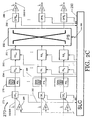
- FIG. 2A A block diagram of an intelligent switching system is illustrated in FIG. 2A.
- Components of the system 200 are shown selectively coupled by a plurality of interconnect lines. Packets enter the system through lines 202. Packets of the forms illustrated in FIGs. 1A, 1B, and 1C are well suited for switching by this system in applications where optical dispersion in not a significant factor. In the first embodiment described herein, it is assumed that the packet is of the form of FIG.1C.
- the system includes a plurality of module types, including:
- a packet enters the system on line 202 . It passes through packet detector 222 , which detects if (and precisely when) the leading edge of a packet has entered the system. This timing signal is sent to de-concentration unit 224 via line 242 and, in one embodiment, also to packet alignment unit 226 via line 244 . The packet continues through the switching system on its journey to output line 218 on the following path:
- the packet de-concentration units 224 and the packet alignment units 226 and 234 do not use the data content of the packet; instead, they use the timing of the "envelope" of the arriving packet.
- a header reader unit 228 employs an optical tap to send a copy of the packet header 180 to the system logic control unit, where it is converted to electronic form.
- Control system 260 employs means and apparatus to read and process header information for subsequent management of all packets and their flow through the switching system components.
- Fixed-delay loop 602 in the header reader acts as an optical packet buffer (an optical FIFO) that delays a packet for a sufficient amount of time for control system 260/280 to complete all operations that determine the subsequent path of the packet.
- Packet re-sequencing units 230 and packet switches 232 are controlled by the system logic control unit (SLC) 260/280.
- the system control unit sends control information (which is based on current traffic rates, packet priority, and target output port status) to re-sequencing units 230 and to switches 232. Understanding of the operation of the intelligent switching system is achieved by understanding each of its component units and their collective functions. The component units will be described in the order in which they receive packets and control signals.
- FIGs. 2B and 2C discussed in the section entitled "Alternate Embodiments".
- FIG. 3 is a block diagram of packet detector 222, optical amplifier 304, and fixed-delay loop (FDL) 276.
- the packet detector receives input on line 202 in the form of serially arriving optical packets, which exit the detector on lines 204.
- the leading edge (or timing bit) of the packet is picked off by an optical tap 302 and copies of it are sent to the de-concentration unit and to the packet alignment unit on lines 242 and lines 244, respectively.
- the packet detector may send the header (or timing information) to the de-concentrator unit, to the packet alignment unit, or to both units in either electronic or optical form.
- line 244 is omitted and the packet alignment unit has its own packet detector.
- the packet detector sends the header information in optical form.
- tap 302 drops only a small portion of the signal into lines 242 and (possibly) 244 ; it may be necessary to amplify the signals on these lines. In one embodiment, this could be accomplished by employing an erbium doped fiber amplifier or similar optical amplifier 304 in lines 242 and 244 ; these lines could be pumped by a single laser (not shown).
- the header it is convenient for the header to be of a specific wavelength ⁇ o so that device 302 can passively strip off a portion of the light of wavelength ⁇ o from the packet
- ⁇ o is the wavelength of the timing bit.
- the time of arrival of the packet is the only control information that is used by the de-concentration unit.
- the packet detector contains a delay loop 276. Accordingly, the packet detector sends a signal, which indicates the precise arrival time of the packet at the de-concentration unit.
- This signal is the timing bit in the header of packet M; it is this bit that governs the timing of the control bit in line 242.
- the header (which includes the timing signal) is sent directly from the packet detector to the de-concentrator. Depending on the technology, it may be necessary that the de-concentrator have an optical to electronic conversion unit.
- FIG. 4A for a schematic diagram of a packet de-concentration unit (DC) 224.
- This unit receives packets on input line 204 and outputs them on a plurality of lines 206.
- the unit receives timing information on line 242.
- FIG. 4B there is a time AM that indicates the length of time that it takes a packet M to pass a point on the fiber.
- the packet width AM is constant for all packets.
- There is minimum gap time ⁇ G which is the time that it takes for the shortest gap between packets to pass a point on the fiber.
- the intelligent switch system 200 sends packets downstream on output lines 218 in a manner preserving the minimum "dark gap" between successive packets.
- the dark gap between successive packets is ⁇ G plus an integer multiple of ( ⁇ G + AM). It is assumed that the intelligent switch 200 receives packets from other switches that use this format. In case the intelligent switch receives packets in another format, it may be necessary that there exist a packet format conversion unit that precedes the intelligent switch, 200.
- the de-concentration unit of FIG . 4A contains a plurality of 1x2 switches arranged in a tree structure. Lithium niobate gates and silicon optical amplifiers (SOA) are suitable for use in this application. Other technologies may be used for these gates as well. There is a single, high-speed 1x2 switch 402 at the root of the tree and a pair of slower speed 1x2 switches 404 at the second level of the tree.
- the tree illustrated in FIG. 4A is a binary tree with two levels. For various applications, the tree can have a number of levels different from two, and the tree can have a branching basis distinct from two. In the model embodiment of FIG.
- the binary tree of two levels enables the de-concentrator to receive packets on one line and output packets on four lines.
- This set of lines exiting a de-concentrator unit DC n (or other unit type), where o ⁇ n ⁇ N-1, will be referred to as an "internal line set", which is labeled L 1n , L 2n , L 3n and L 4n in the drawings for the model embodiment.
- the individual nodes in the tree structure are switched by a de-concentrator control unit 406.
- the control unit receives timing input on line 242 and sends control signals to node switch 402 through line 408 and to node switches 404 through lines 410.
- packet detector 222 sends a signal down line 242 indicating the time of entry of a packet M into the detector. While packet M passes through delay loop 276, the control signal in line 242 arrives at the de-concentrator control unit 406 so that the control signal sent via line 408 arrives at the proper time for switch 402 to change state after packet M has passed through switch 402, but before another packet arrives at switch 402. Alternately stated, switch 402 changes states during the time interval ⁇ G (refer to FIG. 4B ). Similarly, the control signals on lines 410 arrive at switches 404 so that these switches change states between entering packets.
- Node 402 is a high-speed, 1 ⁇ 2 optical switch that is capable of toggling in the brief time period ⁇ G, which is the minimum separation between incoming packets. Notice that the gap between packets entering switch 404 is at least of length AM + 2• ⁇ G. The cost of switch 404 as well as the power that it uses is a function of its switching speed. Therefore, the switch 404 is less expensive than switch 402. The minimum length of the blank space ⁇ B between packets on a line 206 is advantageously increased to at least 4• ⁇ G + 3• ⁇ M. Any switch that directs packets on lines 206 can be slower yet
- FIG. 4B shows a series of consecutive packets passing through the de-concentrator unit.
- the switch that it passes through changes state.
- first node 402 toggles with every packet
- second nodes 404 toggle with every other packet.
- the logic in the unit is simple; timing signal 242 arrives at a node at the beginning of the dark gap.
- control logic 406 immediately toggles node 402, and slightly later, toggles the appropriate second node 404. In both cases, the switches change state immediately after a packet clears the switch.
- FIG. 5A for a block diagram of packet alignment units (PA).
- the system has N alignment units 226, one for each port.
- Each PA is responsible for aligning a set of packets in reference to a system-global timing signal 262 as the packets arrive on internal lines 206 from the corresponding de-concentrator unit 224.
- FIG. 5B illustrates the application of global reference signal 262.
- FIG. 5C is a diagram of packet alignment unit 226 that incorporates optical variable-delay devices along each path.
- the packet logic unit (PLU) 510 uses a timing signal from packet detector 222 sent to it on line 244.
- FIG. 5 D is a diagram of an alignment unit with internal packet detector 522.
- VDL delay loops
- An advantage of the FIG. 5C embodiment is that it requires only one header reader and one packet detector on a packet's end-to-end path.
- PLU 510 keeps track of the state of the de-concentrator switches in order to know on what line a packet is arriving. This is possible because the de-concentrator always switches in a predetermined pattern that is known by the alignment unit.
- An advantage of the embodiment illustrated in FIG. 5D is that PLU 512 may be simpler and there is less likelihood for jitter in the timing.
- FIG. 5D embodiment is presented here.
- Packets arrive at PA 226 on line 206.
- the packet-timing signal is obtained from internal packet detector PD 522 and sent to PLU 512.
- System-wide reference signal 262 connects to the PLU.
- Fixed delay loop 530 provides the PLU with enough time to determine how long to delay each of the four (or fewer) packets that arrive in a given cycle determined by MD 2 .
- PLU 512 Based on the relative arrival time and the global timing signal, PLU 512 calculates how long to delay each packet so as to produce the relative alignment of exiting packets shown in FIG. 5A and sets nodes 524 accordingly.
- Variable delay unit 520 includes a serially connected set of optical delay loops 526 that can be switched in or out of the packet's path.
- the set of lengths of the loops are powers of 2 in this fashion: 1, 2, 4, 8, ..., 2 n-1 .
- the total amount of delay obtained from VDL 520 ranges from zero to the sum of the set, which is (2 n -1) time units.
- a delay of one time unit is the smallest timing adjustment needed to satisfy internal system function and to meet external (downstream) timing requirements. The longest delay is approximately the time associated with four consecutive packets and the gaps between them.
- sets of packets on the internal line sets arrive asynchronously at their respective variable delay units 522. After processing by the alignment unit, all packets on all lines in the intelligent switching system are globally aligned with respect to reference signal 262 .
- FIG. 5E is a packet alignment unit, 284, that is similar in function to PA 520 , except that unit 284 is controlled directly by electronic signals over lines 288 from input port controllers 724 (see FIGs. 2C and 7B).
- FIG. 6 illustrates a header reader and packet delay unit 228.
- Each unit contains a plurality of header readers and delay loops, one for each line 208 in its internal line set Header reader 240 obtains an optical copy of the entire packet or, minimally, packet header 180 for immediate use by control system 260.
- a packet M enters on line 208 and exits on line 210 after passing through fixed delay loop 602.
- This loop is an optical FIFO (first-in, first-out buffer) that delays all packets for a time interval sufficient for control system 260 to perform all scheduling operations for a packet prior to its exiting the FIFO.
- An optical copy of the header information is sent via lines 246 to system control unit 260.
- the header of a packet M includes the following data fields:
- SLC SLC immediately converts the packet header from optical to electronic form (unless O/E conversion has already been performed) and obtains the content of header fields.
- each header bit can be dropped using a chromatic filter or similar device. Otherwise, single-wavelength, serial O/E conversion can be employed.
- the packet header may contain other fields that are used by various embodiments of the intelligent switch. In particular, they may contain multicast bits.
- FIG . 7A is a schematic diagram illustrating the system logic control unit, SLC 260 .
- a central idea in the present patent and in patents No.8 and No. 10 is the scalable, intelligent control of all packets entering the switch fabric, taking into account current traffic rates and QoS requirements. The following is a summary of the means and apparatus for scalable control of a switching system taught in detail in these patents.
- a scalable control unit 706 (in conjunction with IPCs) schedules the timing of all packets entering switch(es) 232 .
- IPC 704 receives and processes header fields (including the QoS field) from all packets entering the system during each cycle.
- SLC 260 employs a scalable means and apparatus to determine at which time slot a given packet can enter optical packet switch 232 without colliding with any other packet.
- a collision occurs when two or more packets are sent to a single output port at the same time.
- a basic reason that the system management is so effective is that there is a logic unit (called a request processor RP) associated with each output port.
- RP considers all of the packets previously scheduled and currently wanting to use the output port and, given their priorities and timing, it schedules when each packet enters the packet switch, desirably preventing collisions. In order for RP 710 to be informed of all incoming packets scheduled for its port, it is necessary to route each request packet to the appropriate RP.
- the interconnect structures defined in patents No.1 to No.7 are self-routing and allow for multiple packets to be routed to the same target. Therefore, they are used here as request switch 708 for effective routing of the request packets to the desired request processors and also used as answer switch 712 for routing the answer packets from the request processors back to the input port controller that issued the request.
- optical header information enters the system logic control unit 260 via lines 246, where it is converted to electronics by O/E converters 702 and then sent via lines 722 to its corresponding input port controller (IPC) 704.
- IPC input port controller
- the IPC performs line-card functions including header lookup and other traffic management functions.
- the input port controller builds a request packet 130 and sends it via line 716 to the request system 706, which is similar in construction and function to those taught in patents No. 8 and 10.
- Sets of headers arrive at system control unit 260 in cycles determined by the global reference signal and in the order H 1 , H 2 , ..., H k .
- the packets associated with the headers in H k are in G k and thus are on the set of lines L kn (0 ⁇ n ⁇ N-1). Moreover, these packets are destined for packet switch PS k 232.
- an input port controller submits a single request for only one switch and receives a single answer from a request processor. The switch number and the packet ID are identified by knowing which set of headers is being processed. Input port controllers are also aware of the time at which each packet will exit the FIFO and enter the re-sequencing unit.
- an input port controller gives a list, AVT 114, of all available times for inserting the associated packet into the proper packet switch 232.
- the AVT times are based on the packet being sent either straight through the re-sequencing unit or else through a set of delay loops within this unit.
- the input port controller updates its AVT list and sends re-sequencing command 150 via line 248 to the re-sequencing unit at the appropriate time.
- the re-sequencing command is sent to and arrives at RS 230 just prior to the packet's exit from the FIFO 602 in the header reader; thus, the logic in the re-sequencing unit has time to set the appropriate switches.
- the RP updates its internal AVT based on packets it scheduled in the current cycle.
- Each request processor 710 controls the flow of packets into the packet switches. Based on information such as QoS and load on the target output port, a request processor selects an available time slot and returns it as TS 122 in an answer packet 140 (via the answer switch AS 712 and line 718) to the input port controller that sent the request. In some cases, it may be necessary to discard the packet. In one embodiment, during each request cycle, request packets are received for only one packet switch 232. Upon receipt of an answer packet by an input port controller, the IPC knows when to send its packet into the packet switch, and thus knows the required delay for the packet.
- SC 714 When a packet is approved by a request processor, it also sends switch-setting information for the packet via line 720 to the switch controller SC 714, either directly or via an input port controller. SC collects switch setting information from all of the request processors and organizes it by switch injection time. Just prior to a set of packets arriving at switches 232, SC sends the appropriate switch-setting information on lines 250 to set the crossbar nodes 902.
- O/E converter 702 is located in header reader 240 (rather than in SLC 260 ).
- lines 246 carry electronic signals. This embodiment advantageously reduces the amount of optical plumbing in the system, replacing it with low-cost, high-speed serial communications technology.
- SLC 260 determines the delay time per packet for all packets, where one time unit MD 2 consists of the time associated with one packet plus its minimum inter-packet gap on a "de-concentrated" line. The outcome of the SLC is the determination of how much time each packet must wait before it can enter packet switch 232, desirably avoiding collisions, while taking into account current traffic rates and QoS demands.
- Input port controller 704 is the final device in this process of determining the delay for a packet that has arrived at its associated input port. Importantly, the packet is moving through the FIFO during the time it takes to determine its delay value. Immediately before the packet exits FIFO 602, the input port controller informs the re-sequencing unit how long to delay the packet.
- re-sequencing unit 230 can be thought of as a set of fixed delay lines terminating at the same point.
- packets may enter the system in the order A, B, C, D, E, and F, and exit in an arbitrary sequence, such as C, F, B, D, A, and E
- packet A is delayed eight periods longer than packet F.
- the external control and interface unit (ECIU) 254 serves at least two functions. First, it has two-way communication with all processing element in the system, including IPCs 704 ( FIG. 7A) or 724 ( FIG. 7B), and RPs 710. Second, it is the interface between the system and the external world, for purposes including administration, operation, maintenance, performance measurements, and diagnoses.
- FIG. 8 for a schematic diagram of packet re-sequencing unit 230.
- a re-sequencing packet is received from SLC 260 on line 248, it is processed by the control unit CTL 810.
- CTL 810 Immediately prior to a packet arriving on line 210, re-sequencing packet 150 informs CTL 810 of the line number and the desired delay.
- CTL sets switches in demux 812, which may be implemented as a binary tree of 1 ⁇ 2 nodes in an arrangement such as indicated in FIG. 4A or by another suitable optical demux design.
- Demux 812 has a plurality of outputs.
- Output 814 causes the packet to be discarded, which could occur when the packet's output port is overloaded with traffic and the packet has a low QoS value.
- FIG. 9A illustrates a crossbar packet switch 232 suitable for use in the intelligent switching system 200.
- Crossbar packet switch 232 receives packets on lines 212, sends packets out on line 214, and receives switch setting information on lines 250.
- the crossbar nominally contains N 2 nodes.
- Node 902 makes an optical connection from an input line to an output line. According to the operation of control system 260, an input connects to zero or one output line, and one output is connected to zero or one input line.
- the system contains K packet switches 232, one switch for each line that exits a de-concentrator unit.
- Packet switch PS k 232 receives and switches all packets arriving on the set of lines L kn , where 1 ⁇ k ⁇ K and 0 ⁇ n ⁇ N-1.
- K 4 and thus, PS 1 switches packets from the set of lines L in , PS 2 switches packets from the set of lines L 2n , PS 3 switches packets from the set of lines L 3n , and PS 4 switches packets from the set of lines L 4n .
- the number of packet switches may be a number different from K. Suitable switches may be of several types:
- MLML switches may be self-routing or may be optical slaves to electronic MLML networks within the switch controller 714 (as described in patent No. 2).
- it is useful to attach optical delay lines of various lengths to the outputs of the innermost rings. The delay lines for all of the nodes at a single angle are equal. In this way, all of the packets are realigned after emerging from the system composed of the MLML network and these delay lines.
- FIG. 9B illustrates a crossbar packet switch 278 where input-to-output connections are set by means of a signal connected to each input port of the crossbar. It receives packets on lines 212, sends packets out on line 214, and receives switch setting information directly from the input port's associated IPC on line 726 (see FIGs. 7B and 2C).
- the crossbar nominally contains N 2 nodes. Node 902 makes an optical connection from an input line to an output line. According to the operation of control system 280, an input connects to zero or one output line.
- FIG. 10 illustrates an additional packet alignment unit 234 .
- This unit is similar in construction and function to the alignment unit 226 illustrated in FIG. 5A.
- Each input line 214 contains a packet detector unit 222 , which sends each incoming packet through a delay loop while sending a timing signal to the corresponding alignment unit 226.
- first alignment unit 226 could be somewhat course in aligning the packets
- the purpose of final alignment unit 234 is to perform a finer alignment that is required prior to the concentration process.
- FIG. 11 is a schematic diagram of a packet concentrator unit 236.
- Four optical lines 216 enter the unit and combine signals until all packets exit on a single fiber. Since the packets have been aligned with respect to a global reference signal, no two input lines send packets into the concentrator at the same time. Importantly, a minimum dark space ⁇ G is always maintained between packets sent downstream. Packets exit the concentrator and the switching system on lines 218. A final optical amplifier, such as shown in FIG. 2C, may be needed here.
- FIG. 2 B An embodiment of the invention with this property is illustrated in FIG. 2 B.
- N lines entering the intelligent switching system N lines internal to the system, and N lines exiting the system. Since the de-concentration step has been eliminated, this embodiment does not contain the following units that are illustrated in FIG. 2A:
- packets exit this system directly from the packet switch 232 on lines 220 .
- packets sent to the system on lines 202 are timed with a world-wide global clock.
- packets arriving on each input line would be evenly spaced on that line, and this spacing would be uniform on each of the N input lines.
- the switch settings in the packet alignment units 284 are determined for aligning the initial set of packets on the N input lines, these setting would remain the same for all future arriving packets. In one embodiment, however, the arrival of the packets is monitored and some minor adjustments to the alignment switches is made, if only on an infrequent basis.
- FIG. 5E illustrates a packet alignment unit 226 that uses optical demux 514 such that a packet passes through one of a plurality of optical delay lines 504 before exiting. Accordingly, the optical packet is delayed over a range determined by the longest delay line, with timing increments related to the number of delay loops in the chosen line.
- FIGs. 2C, 7B and 9B uses electronics whenever possible, thus reducing the amount of optical fibers, connectors, and other optical devices.
- System 270 incorporates these features:
- external control and interface unit (ECIU) 254 has connections to all IPCs and RPs in the system.
- ECIU has a plurality of connections 256 to input ports of request switch 708 and a plurality of connections 258 from output ports of request switch 708, and thus can send an I/O packet to any RP and receive one from any IPC.
- ECIU has a plurality of input and output connections to answer switch 712, and thus can send an I/O packet to any IPC and receive an I/O packet from any RP.
- Uses of this connection capability include:
- IPC-to-IPC communications One use for IPC-to-IPC communications is to generate an optical test packet and use it to gather timing information for paths from one port to another.
- One use for RP-to-IPC communication (in addition to its primary answer-packet function) is to inform an IPC of exceptional conditions such as excess traffic for the output address associated with the RP.
- an IPC has greater processing capabilities than an RP.
- An IPC analyzes the traffic information and can inform the ECIU, which has yet greater processing and analysis capabilities and can use the information in managing the system.
- ECIU functions include operator interface, maintenance, diagnosis and troubleshooting, collecting and analyzing traffic data, putting ports online and offline, and managing user requirements such as QoS service for different traffic types and different ports.
- System 270 ( FIG. 2C) can be employed in a system 290 (FIG. 2D) similar to the system 205 shown in FIG. 2B, where input 202 connects upstream and output 220 connects downstream.
- system 270 can be employed as the "switching core", using packet de-concentrators 224 and concentrators 236 in a fashion similar to their use in system 200 as shown in FIG. 2A.
- lines 206 from the de-concentrator are the input to system 270 and lines 216 are the output from system 270 , connecting directly to packet concentrators 236 .
- the system 200 packet alignment unit 234 is not needed because SLC 280 uses optical feedback 292 in conjunction with a single packet alignment unit 284 to fine-tune the timing of packets so that a second alignment/adjustment step is unnecessary.
- test-packet generator 296, optical feedbacks 292 and 298, and SLC 280 can be suitably incorporated for purposes and uses mentioned above, including system installation, setup, reconfiguration, operation, management, system analysis, diagnosis, and repair functions.
Landscapes
- Engineering & Computer Science (AREA)
- Computer Networks & Wireless Communication (AREA)
- Signal Processing (AREA)
- Physics & Mathematics (AREA)
- Mathematical Physics (AREA)
- Data Exchanges In Wide-Area Networks (AREA)
- Optical Communication System (AREA)
Applications Claiming Priority (1)
| Application Number | Priority Date | Filing Date | Title |
|---|---|---|---|
| US60613604P | 2004-09-01 | 2004-09-01 |
Publications (2)
| Publication Number | Publication Date |
|---|---|
| EP1662724A2 true EP1662724A2 (de) | 2006-05-31 |
| EP1662724A3 EP1662724A3 (de) | 2008-07-02 |
Family
ID=34981448
Family Applications (1)
| Application Number | Title | Priority Date | Filing Date |
|---|---|---|---|
| EP05019058A Withdrawn EP1662724A3 (de) | 2004-09-01 | 2005-09-01 | Mittel und Vorrichtung für eine skallierbare staufreie Vermittlung mit intelligenter Steuerung |
Country Status (4)
| Country | Link |
|---|---|
| US (2) | US20060171386A1 (de) |
| EP (1) | EP1662724A3 (de) |
| JP (1) | JP2006074788A (de) |
| CN (1) | CN1773958A (de) |
Cited By (3)
| Publication number | Priority date | Publication date | Assignee | Title |
|---|---|---|---|---|
| US7835278B2 (en) | 2004-09-01 | 2010-11-16 | Interactic Holdings, Llc | Means and apparatus for a scaleable congestion free switching system with intelligent control III |
| EP1965601A3 (de) * | 2007-02-28 | 2016-05-25 | Fujitsu Ltd. | System und Verfahren zur optischen Übertragung |
| TWI629877B (zh) * | 2016-12-09 | 2018-07-11 | 中華電信股份有限公司 | Intelligent scheduling system for optical buffer front end optical buffer |
Families Citing this family (25)
| Publication number | Priority date | Publication date | Assignee | Title |
|---|---|---|---|---|
| KR20070007769A (ko) * | 2003-10-29 | 2007-01-16 | 인터랙틱 홀딩스 엘엘시 | 에러 정정을 이용하는 높은 병렬 스위칭 시스템 |
| CN101112116B (zh) * | 2004-12-30 | 2011-05-25 | 诺基亚西门子通信有限责任两合公司 | 借助光突发交换网传输数据分组的方法和光突发交换网的网络节点 |
| US8693488B2 (en) * | 2005-09-13 | 2014-04-08 | Nxp B.V. | Method of transmitting messages |
| US20080285971A1 (en) * | 2007-03-23 | 2008-11-20 | Odile Liboiron-Ladouceur | Switch for optical interconnection networks |
| US8849110B2 (en) * | 2007-05-10 | 2014-09-30 | Telefonaktiebolaget Lm Ericsson | Optical node |
| US8040888B1 (en) * | 2007-12-17 | 2011-10-18 | Integrated Device Technology, Inc. | Packet switch with port route tables |
| US20090226185A1 (en) * | 2008-03-06 | 2009-09-10 | International Business Machines Corporation | Fiber optic communications using hue based encoding |
| EP2282427B1 (de) * | 2009-07-31 | 2015-03-04 | Alcatel Lucent | Verfahren zur Synchronisation einer Kundenuhrfrequenz mit einer Serveruhrfrequenz |
| US8320399B2 (en) | 2010-02-26 | 2012-11-27 | Net Optics, Inc. | Add-on module and methods thereof |
| JP5520209B2 (ja) * | 2010-12-16 | 2014-06-11 | 富士通テレコムネットワークス株式会社 | 光パケット交換システムおよび光パケット送信装置 |
| JP5588374B2 (ja) * | 2011-02-08 | 2014-09-10 | 富士通テレコムネットワークス株式会社 | 光パケット交換システム、光パケット交換装置、および光パケット送信装置 |
| JP5439408B2 (ja) * | 2011-02-09 | 2014-03-12 | 富士通テレコムネットワークス株式会社 | 光パケット交換システムおよび光パケット送信装置 |
| JP5411195B2 (ja) * | 2011-03-30 | 2014-02-12 | 富士通テレコムネットワークス株式会社 | 光パケット交換システム |
| US9054827B2 (en) * | 2012-01-27 | 2015-06-09 | Futurewei Technologies, Inc. | Optical switching device using spectral trigger |
| US9674116B2 (en) * | 2012-03-21 | 2017-06-06 | Lightfleet Corporation | Data distribution packet-flow interconnect fabric modular management optimized system |
| US9525621B2 (en) * | 2012-08-29 | 2016-12-20 | Marvell World Trade Ltd. | Semaphore soft and hard hybrid architecture |
| WO2015100636A1 (zh) * | 2013-12-31 | 2015-07-09 | 华为技术有限公司 | 一种环形光缓存器及光信号存入和读取方法 |
| JP6341601B2 (ja) * | 2014-04-01 | 2018-06-13 | 国立研究開発法人情報通信研究機構 | 波長多重分離器とそれを用いた波長多重器 |
| CN105282629A (zh) * | 2014-07-03 | 2016-01-27 | 中兴通讯股份有限公司 | 一种硅光交叉连接的控制方法和装置 |
| CN104601495B (zh) * | 2015-01-30 | 2018-11-30 | 杭州晨晓科技股份有限公司 | 一种扩展物理端口的系统 |
| CN107431535B (zh) * | 2015-04-27 | 2020-04-03 | 华为技术有限公司 | 用于光信号交换的传输路径建立方法及装置 |
| TWI580213B (zh) * | 2015-07-24 | 2017-04-21 | Chunghwa Telecom Co Ltd | A packet-programmable multi-optical delay device for light buffers |
| US10750255B2 (en) * | 2016-04-22 | 2020-08-18 | Huawei Technologies Co., Ltd. | Segment routing for optical networks |
| GB2631124A (en) * | 2023-06-20 | 2024-12-25 | Salience Labs Ltd | A system and method for routing an optical signal |
| US20250175254A1 (en) * | 2023-11-28 | 2025-05-29 | Ciena Corporation | Optical delay compensation in optical modules |
Family Cites Families (20)
| Publication number | Priority date | Publication date | Assignee | Title |
|---|---|---|---|---|
| DE69232305T2 (de) * | 1991-12-16 | 2002-07-25 | AT & T CORP., NEW YORK | Optische Paketvermittlungstelle |
| US5489284A (en) * | 1994-07-15 | 1996-02-06 | Smith & Nephew Richards Inc. | Cannulated modular intramedullary nail |
| DE19502547C1 (de) * | 1995-01-27 | 1996-03-28 | Siemens Ag | Verfahren zum Betrieb einer mehrstufigen NxN-Raumkoppelanordnung |
| US5996020A (en) | 1995-07-21 | 1999-11-30 | National Security Agency | Multiple level minimum logic network |
| US5790545A (en) * | 1996-03-14 | 1998-08-04 | Motorola Inc. | Efficient output-request packet switch and method |
| US5841556A (en) * | 1996-12-26 | 1998-11-24 | Electronics And Telecommunications Research Institute | Optical switching system with combined space and wavelength division multiplex based on the repeated contention resolution technique |
| US6289021B1 (en) | 1997-01-24 | 2001-09-11 | Interactic Holdings, Llc | Scaleable low-latency switch for usage in an interconnect structure |
| US6754207B1 (en) | 1998-01-20 | 2004-06-22 | Interactic Holdings, Llc | Multiple-path wormhole interconnect |
| JP3704438B2 (ja) * | 1998-12-09 | 2005-10-12 | 株式会社日立製作所 | 可変長パケット通信装置 |
| US6556571B1 (en) * | 1999-05-25 | 2003-04-29 | Nec Usa, Inc. | Fast round robin priority port scheduler for high capacity ATM switches |
| US6721315B1 (en) * | 1999-09-30 | 2004-04-13 | Alcatel | Control architecture in optical burst-switched networks |
| JP3627628B2 (ja) * | 2000-06-20 | 2005-03-09 | Kddi株式会社 | 光データ伝送方法及びシステム、光送信装置及び方法並びに光交換機 |
| US7221677B1 (en) | 2000-10-19 | 2007-05-22 | Interactic Holdings, Llc | Scalable apparatus and method for increasing throughput in multiple level minimum logic networks using a plurality of control lines |
| US7016363B1 (en) | 2000-10-19 | 2006-03-21 | Interactic Holdings, Llc | Scaleable interconnect structure utilizing quality-of-service handling |
| US6687253B1 (en) | 2000-10-19 | 2004-02-03 | Interactic Holdings, Llc | Scaleable wormhole-routing concentrator |
| US6587253B2 (en) * | 2001-08-16 | 2003-07-01 | Silicon Light Machines | Enhance thermal stability through optical segmentation |
| JP2003258725A (ja) * | 2002-02-26 | 2003-09-12 | Nec Corp | 光パケットヘッダ識別器並びにこれを用いた光ルータ及び光ルーティング方法 |
| US6956861B2 (en) | 2002-04-16 | 2005-10-18 | Interactics Holdings, Llc | Controlled shared memory smart switch system |
| US20040090964A1 (en) | 2002-11-07 | 2004-05-13 | Coke Reed | Means and apparatus for a scaleable congestion free switching system with intelligent control II |
| US20060171386A1 (en) | 2004-09-01 | 2006-08-03 | Interactic Holdings, Llc | Means and apparatus for a scaleable congestion free switching system with intelligent control III |
-
2005
- 2005-08-31 US US11/214,984 patent/US20060171386A1/en not_active Abandoned
- 2005-09-01 CN CN200510023007.6A patent/CN1773958A/zh active Pending
- 2005-09-01 EP EP05019058A patent/EP1662724A3/de not_active Withdrawn
- 2005-09-01 JP JP2005253757A patent/JP2006074788A/ja active Pending
-
2008
- 2008-11-17 US US12/272,274 patent/US7835278B2/en not_active Expired - Lifetime
Cited By (3)
| Publication number | Priority date | Publication date | Assignee | Title |
|---|---|---|---|---|
| US7835278B2 (en) | 2004-09-01 | 2010-11-16 | Interactic Holdings, Llc | Means and apparatus for a scaleable congestion free switching system with intelligent control III |
| EP1965601A3 (de) * | 2007-02-28 | 2016-05-25 | Fujitsu Ltd. | System und Verfahren zur optischen Übertragung |
| TWI629877B (zh) * | 2016-12-09 | 2018-07-11 | 中華電信股份有限公司 | Intelligent scheduling system for optical buffer front end optical buffer |
Also Published As
| Publication number | Publication date |
|---|---|
| JP2006074788A (ja) | 2006-03-16 |
| CN1773958A (zh) | 2006-05-17 |
| US20060171386A1 (en) | 2006-08-03 |
| US7835278B2 (en) | 2010-11-16 |
| US20090067837A1 (en) | 2009-03-12 |
| EP1662724A3 (de) | 2008-07-02 |
Similar Documents
| Publication | Publication Date | Title |
|---|---|---|
| US7835278B2 (en) | Means and apparatus for a scaleable congestion free switching system with intelligent control III | |
| Xiong et al. | Design and analysis of optical burst-switched networks | |
| US20020141398A1 (en) | Methods to process and forward control packets in OBS/LOBS and other burst switched networks | |
| Zhang et al. | Slotted optical burst switching (SOBS) networks | |
| US7139253B2 (en) | Packet switches | |
| US7801034B2 (en) | System and method for bandwidth allocation in an optical light-trail | |
| Yoo et al. | The effect of limited fiber delay lines on QoS performance of optical burst switched WDM networks | |
| Widjaja et al. | Simplified layering and flexible bandwidth with TWIN | |
| Papazoglou et al. | Design alternatives for optical-packet-interconnection network architectures | |
| HK1095444A (en) | Means and apparatus for a scaleable congestion free switching system with intelligent control | |
| Maach et al. | Congestion control and contention elimination in optical burst switching | |
| Sheeshia et al. | Synchronous optical burst switching | |
| Li et al. | Novel resource reservation schemes for optical burst switching | |
| Myers et al. | Performance of the Just-Enough-Time (JET) scheme for optical burst switching | |
| Rahbar et al. | Slot contention resolution for distributed TDM scheduling in an optical star network | |
| Yu et al. | Enhanced fat tree-an optical/electrical hybrid interconnection for data center | |
| Garg | Managing contention avoidance and maximizing throughput in OBS network | |
| Shuo | Analysis and synthesis of optical burst switched networks | |
| Jin et al. | APOSN: operation, modeling and performance evaluation | |
| Maach et al. | Contention avoidance in optical burst switching | |
| Riadi et al. | A controlled retransmission scheme for optical burst switching over star networks | |
| Cuda et al. | Getting routers out of the core: Building an optical wide area network with" multipaths" | |
| Reza et al. | Throughput and delay performance analysis of feed-forward and feedback shared fiber delay line based hybrid buffering optical packet switch | |
| Qiu | Performance analysis of a selective burst discarding scheme for deflection routing in OBS networks | |
| Shivae et al. | Quality of service provisioning in metropolitan area networks using optical burst switching |
Legal Events
| Date | Code | Title | Description |
|---|---|---|---|
| PUAI | Public reference made under article 153(3) epc to a published international application that has entered the european phase |
Free format text: ORIGINAL CODE: 0009012 |
|
| AK | Designated contracting states |
Kind code of ref document: A2 Designated state(s): AT BE BG CH CY CZ DE DK EE ES FI FR GB GR HU IE IS IT LI LT LU LV MC NL PL PT RO SE SI SK TR |
|
| AX | Request for extension of the european patent |
Extension state: AL BA HR MK YU |
|
| REG | Reference to a national code |
Ref country code: HK Ref legal event code: DE Ref document number: 1095444 Country of ref document: HK |
|
| PUAL | Search report despatched |
Free format text: ORIGINAL CODE: 0009013 |
|
| AK | Designated contracting states |
Kind code of ref document: A3 Designated state(s): AT BE BG CH CY CZ DE DK EE ES FI FR GB GR HU IE IS IT LI LT LU LV MC NL PL PT RO SE SI SK TR |
|
| AX | Request for extension of the european patent |
Extension state: AL BA HR MK YU |
|
| AKX | Designation fees paid | ||
| STAA | Information on the status of an ep patent application or granted ep patent |
Free format text: STATUS: THE APPLICATION IS DEEMED TO BE WITHDRAWN |
|
| 18D | Application deemed to be withdrawn |
Effective date: 20090108 |
|
| REG | Reference to a national code |
Ref country code: DE Ref legal event code: 8566 |
|
| REG | Reference to a national code |
Ref country code: HK Ref legal event code: WD Ref document number: 1095444 Country of ref document: HK |