EP1662572B1 - Flachbildschirm und Verfahren zu dessen Herstellung - Google Patents
Flachbildschirm und Verfahren zu dessen Herstellung Download PDFInfo
- Publication number
- EP1662572B1 EP1662572B1 EP05110991.6A EP05110991A EP1662572B1 EP 1662572 B1 EP1662572 B1 EP 1662572B1 EP 05110991 A EP05110991 A EP 05110991A EP 1662572 B1 EP1662572 B1 EP 1662572B1
- Authority
- EP
- European Patent Office
- Prior art keywords
- enclosure
- emitting device
- light emitting
- sealing
- edges
- Prior art date
- Legal status (The legal status is an assumption and is not a legal conclusion. Google has not performed a legal analysis and makes no representation as to the accuracy of the status listed.)
- Expired - Lifetime
Links
Images


Classifications
-
- H—ELECTRICITY
- H05—ELECTRIC TECHNIQUES NOT OTHERWISE PROVIDED FOR
- H05B—ELECTRIC HEATING; ELECTRIC LIGHT SOURCES NOT OTHERWISE PROVIDED FOR; CIRCUIT ARRANGEMENTS FOR ELECTRIC LIGHT SOURCES, IN GENERAL
- H05B33/00—Electroluminescent light sources
- H05B33/02—Details
- H05B33/04—Sealing arrangements, e.g. against humidity
-
- H—ELECTRICITY
- H10—SEMICONDUCTOR DEVICES; ELECTRIC SOLID-STATE DEVICES NOT OTHERWISE PROVIDED FOR
- H10K—ORGANIC ELECTRIC SOLID-STATE DEVICES
- H10K59/00—Integrated devices, or assemblies of multiple devices, comprising at least one organic light-emitting element covered by group H10K50/00
- H10K59/80—Constructional details
- H10K59/87—Passivation; Containers; Encapsulations
-
- H—ELECTRICITY
- H05—ELECTRIC TECHNIQUES NOT OTHERWISE PROVIDED FOR
- H05B—ELECTRIC HEATING; ELECTRIC LIGHT SOURCES NOT OTHERWISE PROVIDED FOR; CIRCUIT ARRANGEMENTS FOR ELECTRIC LIGHT SOURCES, IN GENERAL
- H05B33/00—Electroluminescent light sources
- H05B33/10—Apparatus or processes specially adapted to the manufacture of electroluminescent light sources
-
- H—ELECTRICITY
- H10—SEMICONDUCTOR DEVICES; ELECTRIC SOLID-STATE DEVICES NOT OTHERWISE PROVIDED FOR
- H10K—ORGANIC ELECTRIC SOLID-STATE DEVICES
- H10K50/00—Organic light-emitting devices
- H10K50/80—Constructional details
- H10K50/84—Passivation; Containers; Encapsulations
-
- H—ELECTRICITY
- H10—SEMICONDUCTOR DEVICES; ELECTRIC SOLID-STATE DEVICES NOT OTHERWISE PROVIDED FOR
- H10K—ORGANIC ELECTRIC SOLID-STATE DEVICES
- H10K50/00—Organic light-emitting devices
- H10K50/80—Constructional details
- H10K50/84—Passivation; Containers; Encapsulations
- H10K50/841—Self-supporting sealing arrangements
-
- H—ELECTRICITY
- H10—SEMICONDUCTOR DEVICES; ELECTRIC SOLID-STATE DEVICES NOT OTHERWISE PROVIDED FOR
- H10K—ORGANIC ELECTRIC SOLID-STATE DEVICES
- H10K50/00—Organic light-emitting devices
- H10K50/80—Constructional details
- H10K50/84—Passivation; Containers; Encapsulations
- H10K50/842—Containers
- H10K50/8426—Peripheral sealing arrangements, e.g. adhesives, sealants
-
- H—ELECTRICITY
- H10—SEMICONDUCTOR DEVICES; ELECTRIC SOLID-STATE DEVICES NOT OTHERWISE PROVIDED FOR
- H10K—ORGANIC ELECTRIC SOLID-STATE DEVICES
- H10K50/00—Organic light-emitting devices
- H10K50/80—Constructional details
- H10K50/84—Passivation; Containers; Encapsulations
- H10K50/844—Encapsulations
-
- H—ELECTRICITY
- H10—SEMICONDUCTOR DEVICES; ELECTRIC SOLID-STATE DEVICES NOT OTHERWISE PROVIDED FOR
- H10K—ORGANIC ELECTRIC SOLID-STATE DEVICES
- H10K50/00—Organic light-emitting devices
- H10K50/80—Constructional details
- H10K50/84—Passivation; Containers; Encapsulations
- H10K50/846—Passivation; Containers; Encapsulations comprising getter material or desiccants
-
- H—ELECTRICITY
- H10—SEMICONDUCTOR DEVICES; ELECTRIC SOLID-STATE DEVICES NOT OTHERWISE PROVIDED FOR
- H10K—ORGANIC ELECTRIC SOLID-STATE DEVICES
- H10K59/00—Integrated devices, or assemblies of multiple devices, comprising at least one organic light-emitting element covered by group H10K50/00
- H10K59/80—Constructional details
- H10K59/87—Passivation; Containers; Encapsulations
- H10K59/871—Self-supporting sealing arrangements
- H10K59/8722—Peripheral sealing arrangements, e.g. adhesives, sealants
-
- H—ELECTRICITY
- H10—SEMICONDUCTOR DEVICES; ELECTRIC SOLID-STATE DEVICES NOT OTHERWISE PROVIDED FOR
- H10K—ORGANIC ELECTRIC SOLID-STATE DEVICES
- H10K59/00—Integrated devices, or assemblies of multiple devices, comprising at least one organic light-emitting element covered by group H10K50/00
- H10K59/80—Constructional details
- H10K59/87—Passivation; Containers; Encapsulations
- H10K59/873—Encapsulations
-
- H—ELECTRICITY
- H10—SEMICONDUCTOR DEVICES; ELECTRIC SOLID-STATE DEVICES NOT OTHERWISE PROVIDED FOR
- H10K—ORGANIC ELECTRIC SOLID-STATE DEVICES
- H10K59/00—Integrated devices, or assemblies of multiple devices, comprising at least one organic light-emitting element covered by group H10K50/00
- H10K59/80—Constructional details
- H10K59/87—Passivation; Containers; Encapsulations
- H10K59/874—Passivation; Containers; Encapsulations including getter material or desiccant
-
- H—ELECTRICITY
- H10—SEMICONDUCTOR DEVICES; ELECTRIC SOLID-STATE DEVICES NOT OTHERWISE PROVIDED FOR
- H10K—ORGANIC ELECTRIC SOLID-STATE DEVICES
- H10K2102/00—Constructional details relating to the organic devices covered by this subclass
- H10K2102/301—Details of OLEDs
- H10K2102/311—Flexible OLED
-
- H—ELECTRICITY
- H10—SEMICONDUCTOR DEVICES; ELECTRIC SOLID-STATE DEVICES NOT OTHERWISE PROVIDED FOR
- H10K—ORGANIC ELECTRIC SOLID-STATE DEVICES
- H10K59/00—Integrated devices, or assemblies of multiple devices, comprising at least one organic light-emitting element covered by group H10K50/00
- H10K59/10—OLED displays
- H10K59/12—Active-matrix OLED [AMOLED] displays
Definitions
- the present invention relates to a flat panel display and a method of manufacturing a flat panel display, and more particularly, to a sealed, flexible flat panel display and a method of manufacturing the sealed, flexible flat panel display.
- FPDs flat panel displays
- OELDs organic electroluminescent displays
- TFT-LCD thin film transistor liquid crystal displays
- a flexible substrate is used to produce thin, flexible FPDs, and a plastic substrate is typically used as the flexible substrate.
- FPDs undergo complicated manufacturing processes, such as formation of an organic film, a thin film transistor layer, an electrode layer, an orientation layer, etc., on a substrate, depending on the particular characteristics of the FPD, when using a plastic substrate, such processes may deform the plastic substrate or thin layers formed on the plastic substrate.
- plastic is generally less dense than glass.
- a plastic substrate may not effectively prevent permeation of water or air.
- a plastic substrate may be coated with a barrier layer to block permeation of water or air.
- U.S. Patent Nos. 6,268,695 and 6,497,598 disclose an organic light emitting device encapsulated in a film including polymer layers and a ceramic layer interposed between the polymer layers.
- U.S. Patent No. 6,413,645 discloses an organic light emitting device encapsulated in a stack of at least one polymer layer and at least one inorganic layer.
- U.S. Patent No. 6,522,067 discloses an organic light emitting device encapsulated in a stack of at least one barrier layer and at least one polymer layer.
- U.S. Patent No. 6,548,912 discloses a microelectronic device encapsulated in a stack of at least one barrier layer and at least one polymer layer.
- 6,570,325 disclosed an organic light emitting device encapsulated in a stack where a barrier layer is interposed between decoupling layers.
- U.S. Patent No. 6,573,652 discloses a display device encapsulated in a stack of at least one barrier layer and at least one polymer layer.
- the barrier layer which includes an inorganic film, to encapsulate an FPD
- the barrier layer may be too thin, which may degrade its durability.
- the limit of a process temperature is low, so that manufacturing the FPD may be difficult.
- Korean Patent Publication No. 2003-2946 discloses an organic light emitting device sealed by plastic that is heated and press-fitted onto the light emitting device instead of being adhered by an adhesive.
- the plastic may not completely prevent permeation of water and air. This results in degradation of the lifespan and durability of the organic light emitting device.
- U.S. Patent Publication No. 2003/0027369 A1 discloses a method of making a light emitting device that is vacuum-sealed with a bag-like plastic film inside of which inorganic insulating films, which can prevent oxygen or water from penetrating therein, and an organic insulating film, which has a smaller internal stress than the inorganic insulating films, are laminated.
- the plastic film having the inorganic insulative film bends, the inorganic insulative film may crack, leading to degradation of the ability of preventing permeation of water and air.
- Japanese Patent Publication No. 1993-144569 discloses a method of manufacturing a light emitting device that is sealed by forming a thermoplastic hygroscopic film on both sides of the light emitting device, heating and press-fitting the film onto the light emitting device to seal all of the device's peripheral parts, and then covering the sealed light emitting device with an outer cover film.
- the thermoplastic hygroscopic film and the outer cover film may not completely prevent permeation of water and air.
- the present invention provides a flexible flat panel display according to claim 1 that may be simply manufactured and that may block water and oxygen, and a method of manufacturing the flat panel display according to claim 12.
- the present invention discloses a flat panel display including a light emitting device having a sealed image display area/portion.
- the flat display panel further comprises a clip coupled to an exterior surface of the curved portion of the enclosure.
- the enclosure is flexible.
- the enclosure comprises a single sheet.
- the enclosure comprises three edge where sealing occurs.
- the flat display panel further comprises an adhering unit interposed between the enclosure and the light emitting device.
- the flat display panel further comprises a moisture absorbing unit interposed between the enclosure and the light emitting device.
- the enclosure comprises a plastic film including an inorganic layer.
- the inorganic layer is formed of at least one material selected from the group consisting of silicon, metal oxide, metal nitride, metal carbide, metal oxynitride, a ceramic derivative of silicon, a ceramic derivative of metal, diamond-like carbon, and a compound thereof.
- the plastic film further includes a polymer layer, the polymer layer being formed of at least one material selected from the group consisting of an organic polymer, an inorganic polymer, an organometallic polymer, and a hybrid organic/inorganic polymer.
- the substrate is formed of one of glass, plastic, and metal.
- a sealing element seals the image display area by being coupled to a substrate of the light emitting device; and wherein the sealing element is a plate.
- a sealing element seals the image display area by being coupled to a substrate of the light emitting device; and wherein the sealing element is a film.
- the step of sealing edge of the enclosure comprises: coating the edge of the enclosure with an adhesive; sealing the edge of the enclosure with at least a portion of the edge open; exhausting air from the enclosure; and sealing the open portion.
- the step of sealing edge of the enclosure comprises: coating the edge of the enclosure with an adhesive; sealing the edge of the enclosure with at least a portion of the edge open; inserting an inert gas into the enclosure; and sealing the open portion.
- the step of sealing edge of the enclosure comprises: coating the edge of the enclosure with an adhesive; forming a vacuum in an internal space formed by the enclosure; and sealing the edge of the enclosure coated with the adhesive.
- the step of sealing edge of the enclosure comprises: coating the edge of the enclosure with an adhesive; forming an inert gas ambient in an internal space formed by the enclosure; and sealing the edge of the enclosure coated with the adhesive.
- the method further comprises forming an adhering unit on a surface of the enclosure to seat the light emitting device thereon.
- the method further comprises forming a moisture absorbing unit on a surface of the enclosure to seat the light emitting device thereon.
- the enclosure is flexible.
- the enclosure is a plastic film including an inorganic layer.
- the inorganic layer is formed of at least one material selected from the group consisting of silicon, metal oxide, metal nitride, metal carbide, metal oxynitride, a ceramic derivative of silicon, a ceramic derivative of metal, diamond-like carbon, and a compound thereof.
- the plastic film further includes a polymer layer, the polymer layer being formed of at least one material selected from the group consisting of an organic polymer, an inorganic polymer, an organometallic polymer, and a hybrid organic/inorganic polymer.
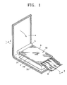
- FIG. 1 is an exploded perspective view of a flat panel display according to an embodiment of the present invention.
- FIG. 2 is a cross-section taken along line I-I of FIG. 1 . While the flat panel display of FIG. 1 and FIG. 2 is shown as an organic electroluminescent display, it may be one of various types of flat panel displays, such as, liquid crystal displays, inorganic light emitting displays, electron emission displays, etc.
- the flat panel display includes an enclosure 4 and a light-emitting device 10 arranged inside the enclosure 4. At least one supporter 5 is placed on an edge of the light emitting device 10.
- the light emitting device 10 includes a substrate 1, an image display portion 2 formed on the substrate 1 and including an organic light-emitting device, and a sealing element 3 coupled to the substrate 1 to protect the image display portion 2 from the external atmosphere.
- the image display portion 2 which includes the organic light emitting device, displays an image.
- organic light emitting devices may be used as the organic light emitting device included in the image display portion 2.
- a simple passive-matrix (PM) organic light emitting device or an active-matrix (AM) organic light emitting device, which has a thin film transistor (TFT) layer may be used as the organic light emitting device included in the image display portion 2.
- PM passive-matrix
- AM active-matrix
- TFT thin film transistor
- FIG. 3 shows an example of a PM organic light emitting device.
- a first electrode layer 21 is formed on a substrate 1 in strips, and an organic layer 23 and a second electrode layer 24 are sequentially formed on the first electrode layer 21.
- An insulative layer 22 may be interposed between adjacent first electrode strips 21, and the second electrode layer 24 may be formed in strips that cross the first electrode strips 21 at right angles.
- the organic layer 23 may be a monomer organic layer or a polymer organic layer.
- a hole injection layer (HIL), a hole transport layer (HTL), an emissive layer (EML), an electron transport layer (ETL), an electron injection layer (EIL), etc. may be stacked in a single or complex structure.
- the organic material may be various materials including copper phthalocyanine (CuPc), N,N-Di(naphthalene-1-yl)-N,N' -diphenyl-benzidine;NPB, and tris-8-hydroxyquinoline aluminum (Alq3).
- the monomer organic layer may be formed by vacuum deposition.
- a polymer organic layer usually includes an HTL and an EML.
- the HTL may be PEDOT
- the EML may be formed of a polymer organic material, such as poly-phenylenevinylene (PPV) or polyfluorene, by screen printing, inkjet printing, etc.
- the first electrode layer 21 serves as an anode electrode
- the second electrode layer 24 serves as a cathode electrode.
- the first electrode layer 21 may serve as the cathode
- the second electrode layer 24 may serve as the anode.
- the second electrode layer 24 may be a transparent indium-tin-oxide (ITO) electrode.
- the first electrode layer 21 may be a transparent electrode.
- the second electrode layer 24 may be produced by forming a thin semi-permeable metal film, such as, Mg, Ag, etc., and depositing transparent ITO on the thin semi-permeable film.
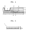
- FIG. 4 shows an example of an AM organic light emitting device.
- each pixel of the image display portion 2 shown in FIG. 1 and FIG. 2 has a TFT and a self-luminant electroluminescent (EL) device.
- EL electroluminescent
- the TFT included in each pixel need not have the exemplary structure shown in FIG. 4 . Additionally, the number of TFTs included in each pixel and the structure of each TFT may be changed into various forms.
- the AM organic light emitting device is described in greater detail below.
- a TFT is formed on the substrate 1.
- the TFT includes an active layer 12 formed on the substrate 1, a gate insulating film 13 formed on the active layer 12, and a gate electrode 14 formed on the gate insulating film 13.
- An inter-insulator 15 is formed on the gate electrode 14 and the gate insulating film 13.
- a source electrode 16 and a drain electrode 17 are formed on the inter-insulator 15 and are coupled with a source area and a drain area, respectively, of the active layer 12 via contact holes.
- a passivation film 18 of an insulative material is formed on the source and drain electrodes 16 and 17, and an insulative pixel defining film 19 is formed on the passivation film 18.
- the passivation film 18 may have a single-layered structure or a multi-layered structure.
- At least one capacitor is coupled to the TFT.
- the organic light emitting device may emit red, green or blue light according to an organic material and a flow of current to display image information.
- the organic light emitting device includes the first electrode layer 21 coupled to the drain electrode 17 of the TFT and receiving positive power from the drain electrode 17, a second electrode layer 24 covering the entire area of each pixel and supplying negative power to the pixel, and an organic layer 23 interposed between the first and second electrode layers 21 and 24 and emitting light.
- the first electrode layer 21 may be a reflective electrode including a reflective layer of Ag, Mg, Al, Pt, Pd, Au, Ni, Nd, Ir, Cr, or a compound thereof, and ITO, IZO, ZnO, or In 2 O 3 deposited on the reflective layer.
- the second electrode layer 24 may be a transparent electrode formed by depositing a metal with a small work function, such as Li, Ca, LiF/Ca, LiF/Al, Al, Mg, or a compound thereof, in a direction facing the organic layer 23 and forming an auxiliary electrode layer or a bus electrode line of a material suitable for forming a transparent electrode, such as ITO, IZO, ZnO, or In 2 O 3 , on the metal.
- a metal with a small work function such as Li, Ca, LiF/Ca, LiF/Al, Al, Mg, or a compound thereof
- the second electrode layer 24 need not be deposited on the entire surface of each pixel. Rather, it may be formed to have various patterns. As described above, the first and second electrode layers 21 and 24 may be formed in strips that are orthogonal to each other.
- the TFT structure and the organic light emitting device structure are not limited to the above-described embodiment as they may be modified into various structures.
- the substrate 1 on which the image display portion 2 is formed may be transparent or opaque. Glass or plastic may be used for the transparent substrate 1, and glass, plastic, or metal may be used for the opaque substrate 1. When the substrate 1 is transparent, the image display portion 2 may emit light toward the substrate 1 and/or the sealing element 3. When the substrate 1 is opaque, the image display portion 2 emits light toward the sealing element 3.
- the substrate 1 may be flexible.
- the substrate 1 may comprise a plastic material.
- the substrate 1 may be made of various materials including thin glass or metal.
- plastic materials used to form the substrate 1 may include polyethylene terephthalate (PET), polyethylene naphthalate (PEN), polycarbonate (PC), polyether sulfone (PES), etc.
- PET polyethylene terephthalate
- PEN polyethylene naphthalate
- PC polycarbonate
- PES polyether sulfone
- the image display portion 2 may be formed directly on the substrate 1, as shown in FIG. 3 and FIG. 4 , so that a protection layer for protecting the image display portion 2 from water and air is not formed on the substrate 1. Since such a protection layer includes an inorganic layer, which may be difficult to form, it is preferable that a protection layer is not formed on the substrate 1 having the image display portion 2 formed directly thereon.
- the sealing element 3, which seals the image display portion 2 may be transparent or opaque.
- the sealing element 3 may be formed of either a transparent material or an opaque material.
- the sealing element 3 is formed of a transparent material.
- Glass or plastic may be used to form a transparent sealing element 3, and glass, plastic, or metal may be used to form an opaque sealing element 3.
- the substrate 1, the image display portion 2, and the sealing element 3 are all shown as having plate shapes.
- the sealing element 3 is a plastic plate
- the plastic plate may have no protection layers, as in the case where the substrate 1 is made of plastic.
- the present invention is not limited to this embodiment, and the sealing element 3 may be a plastic plate having a protection layer formed on at least one surface thereof. Such a protection layer will be described in greater detail later.
- the first sealant 71 may be a thermosetting adhesive and/or an ultraviolet thermosetting adhesive.
- the first sealant 71 may be frit glass.
- a moisture absorbing agent may be included in the space between the substrate 1 and the sealing element 3.
- the moisture absorbing agent which absorbs oxygen and water, may be made of barium oxide, calcium oxide, or porous oxide.
- the porous oxide include porous silica, hydrated amorphous alumina, or a compound thereof.
- the hydrated amorphous alumina may be at least one of bohemite (AIOOH) and bayerite (Al(OH) 3 ).
- the moisture absorbing agent may be any other material that absorbs oxygen and water.
- Pads (not shown) coupled to the image display portion 2 are exposed on one end of the substrate 1.
- a flexible printed circuit-board (FPC) 6 is bonded to the pads.
- the FPC 6 provides power to the image display portion 2 and is coupled to external electronic devices to provide various signals to the image display portion 2. After forming the light-emitting device 10, the light-emitting device 10 may be seated on the enclosure 4.
- An adhering unit 73 may be formed on the enclosure 4, and the substrate 1 of the light-emitting device 10 is bonded to the adhering unit 73 to be seated on the enclosure 4.
- the adhering unit 73 may be a thermosetting adhesive and/or an ultraviolet thermosetting adhesive.
- the adhering unit 73 may be double-sided adhering tape.
- the adhering unit 73 may contain the above-described moisture absorbing agent. Additionally, the adhering unit 73 may be replaced by a moisture absorbing unit, such as, a moisture absorbing agent or a moisture absorbing tape.
- the enclosure 4 is bent as shown in FIG. 1 and FIG. 2 to seal the light-emitting device 10. Because the enclosure 4 has a second sealant 72 formed along its edge, two ends of the enclosure 4 may be bonded together.
- the second sealant 72 may be a thermosetting adhesive and/or an ultraviolet thermosetting adhesive. Alternatively, the second sealant 72 may be frit glass.
- the enclosure 4 is bent to seal the light-emitting device 10, it is preferred that the enclosure 4 is flexible.
- the enclosure 4 comprises a single sheet to seal the light-emitting device 10
- only three portions need to be bonded. Having fewer bonded portions may improve the sealing effect.
- the enclosure 4 may include a base film 41 having a protection layer 42.
- the base film 41 may be made of plastic.
- the protection layer 42 may be formed of a transparent material that blocks water and air.
- the protection layer 42 includes at least one inorganic layer 421, which may be formed of metal oxide, metal nitride, metal carbide, metal oxynitride, or a compound thereof.
- the metal oxide include silica, alumina, titania, indium oxide, tin oxide, indium tin oxide, and a combination thereof.
- the metal nitride include aluminum nitride, silicon nitride, and a combination thereof.
- the metal carbide may be a silicon carbide, and the metal oxynitride may be silicon oxynitride.
- the inorganic layer 421 may be formed of silicon, a ceramic derivative of silicon, or a ceramic derivative of metal. Furthermore, the inorganic layer 421 may be formed of any inorganic material that can block permeation of water and oxygen, for example, diamond-like carbon (DLC).
- DLC diamond-like carbon
- the inorganic layer 421 may be formed by vacuum deposition. In this case, pores included in the inorganic layer 421 may keep growing. Hence, a polymer layer 422 may be included to prevent the pores from continuously growing at the initial locations.
- the polymer layer 422 may be formed of an organic polymer, an inorganic polymer, an organometallic polymer, a hybrid organic/inorganic polymer, etc.
- the protection layer 42 may be formed on an inside surface of the base film 41, as shown in FIG. 5 , and it may also be formed on an outside surface thereof.
- the enclosure 4 shown in FIG. 5 is preferably transparent.
- the protection layer 42 is also preferably formed of a transparent material.
- the enclosure 4 may be sealed by thermal pressing instead of using the second sealant 72.
- a part of the enclosure 4 is thermally pressed so that the enclosure 4 may not include the protection layer 42 anymore.
- This thermal pressing preferably occurs on a part of the enclosure 4 to which the FPC 6 is bonded, because the part of the enclosure 4 can be bonded to the FPC 6.
- the protection layer 42 can be formed using a separate process.
- the process of making an encapsulated organic light-emitting device may be simplified, and the process of forming the protection layer 42 may also be simplified.
- the supporter 5 is interposed between the light emitting device 10 and the enclosure 4 at a location corresponding to the bent portion of the enclosure 4 so that the bent portion of the enclosure 4 is not folded too flat.
- An exterior surface of the supporter 5 is rounded so that the enclosure 4 can be smoothly bent along the round exterior surface of the supporter 5. As FIG. 1 shows, the supporter 5 is coupled to an edge of the light emitting device 10.
- the supporter 5 may be formed of metal or plastic. Alternatively, the supporter 5 may be formed by depositing silicon or other like materials and hardening the same.
- the supporter 5 prevents excessive bending of the enclosure 4, the inorganic layer 421 of the protection layer 42 may not be damaged, thereby enhancing blockage of water and air. Additionally, because the supporter 5 covers a lateral side of the light emitting device 10, the supporter 5 can more effectively protect the light emitting device 10 from an external impact.
- the space formed by the bent enclosure 4 may be vacuum-sealed or filled with an inert gas.
- the enclosure 4 may be sealed within a chamber that keeps a predetermined vacuum atmosphere.
- the enclosure 4 may be sealed within a chamber into which the inert gas is injected.
- edge of the enclosure 4 may be coated with the second sealant 72, and the enclosure 4 is sealed with at least a portion of the edge of the enclosure 4 open. Thereafter, air may be exhausted from the enclosure 4 through the open portion, and then the open portion of the enclosure 4 is sealed. In this case, sealing occurs twice, but the vacuum sealing of the space formed by the bent enclosure 4 may be smoothly performed.
- the enclosure 4 is sealed with at least a portion of the edge of the enclosure 4 open, the inert gas is injected into the enclosure 4 through the open portion, and then the open portion of the enclosure 4 is sealed.
- a clip 8 may be further coupled to an exterior surface of the bent portion of the enclosure 4 to more firmly fix the enclosure 4, the light emitting device 10, and the supporter 5.
- the clip 8 may be formed of metal or plastic.
- a portion of the enclosure 4 on which the substrate 1 is formed may be flat.
- the sealing element 3 may be a sealing film instead of a sealing plate as in the previous embodiments.
- the film-shaped sealing element 3 may include at least one inorganic layer and at least one polymer layer. Similar to structure of the enclosure 4, the sealing film 3 may be a plastic film on which a protection layer is formed.
- the inorganic layer of the sealing film 3 may be formed of a transparent material that blocks water and air, examples of which include metal oxide, metal nitride, metal carbide, metal oxynitride, and a compound thereof.
- the metal oxide include silica, alumina, titania, indium oxide, tin oxide, indium tin oxide, and a combination thereof.
- the metal nitride include aluminum nitride, silicon nitride, and a combination thereof.
- the metal carbide may be a silicon carbide, and the metal oxynitride may be silicon oxynitride.
- the inorganic layer may be formed of silicon, a ceramic derivative of silicon, or a ceramic derivative of metal.
- the inorganic layer may be formed of any inorganic material that can block permeation of water and oxygen for example, DLC.
- the polymer layer included in the sealing film 3 of FIG. 8 may be formed of an organic polymer, an inorganic polymer, an organometallic polymer, a hybrid organic/inorganic polymer, etc.
- Embodiments of the present invention may be applied to organic light emitting displays, as well as to other various flat panel displays, such as, liquid crystal displays, inorganic light emitting displays, electron emission displays, etc.
- a flat panel display according to an embodiment of the present invention may have the following advantages. First, an ultra thin, flexible flat panel display may be simply manufactured.
- a flexible flat panel display may still have high moisture resistance and high air resistance.
- sealing is enhanced because fewer edge of an enclosure have to be sealed.
- the enclosure is bent without a flatly folded portion to prevent damage to a protection layer of the enclosure.
Landscapes
- Physics & Mathematics (AREA)
- Optics & Photonics (AREA)
- Engineering & Computer Science (AREA)
- Manufacturing & Machinery (AREA)
- Electroluminescent Light Sources (AREA)
- Devices For Indicating Variable Information By Combining Individual Elements (AREA)
Claims (19)
- Flachbildschirm, aufweisend:eine lichtemittierende Vorrichtung (10), die einen abgedichteten Bildanzeigeabschnitt (2) aufweist,wobei der Bildanzeigeabschnitt (2) durch ein Dichtungselement (3) und ein erstes Dichtungsmittel (71) abgedichtet ist, wobei Ränder des Dichtungselements (3) mittels des ersten Dichtungsmittels (71) mit einem Substrat (1) der lichtemittierenden Vorrichtung (10) gekoppelt sind; undwobei der Flachbildschirm ferner eine Umhüllung (4) aufweist, die einen eine Schutzschicht aufweisenden Film aufweist, und die Umhüllung (4) gebogen ist, um einen Raum aufzuweisen, in dem die lichtemittierende Vorrichtung (10) abgedichtet ist, wobei der gebogene Abschnitt der Umhüllung (4) gerundet ist,dadurch gekennzeichnet, dass der gebogene Abschnitt der Umhüllung (4) von einem Träger (5), der zwischen der lichtemittierenden Vorrichtung (10) und dem gebogenen Abschnitt der Umhüllung (4) angeordnet ist, getragen wird, wobei der Träger (5) mit einem Rand der lichtemittierenden Vorrichtung (10) gekoppelt und auf diesem platziert ist, wobei der Träger (5) eine gerundete Außenfläche aufweist.
- Flachbildschirm nach Anspruch 1, wobei die Umhüllung (4) einen Kunststofffilm, mit einer anorganischen Schicht aufweist.
- Flachbildschirm nach Anspruch 1, wobei der Flachbildschirm ferner eine Klammer (8) aufweist, die an eine Außenfläche des gebogenen Abschnitts der Umhüllung (4) verkoppelt ist.
- Flachbildschirm nach Anspruch 1, wobei die Umhüllung (4) eine einzelne Platte aufweist.
- Flachbildschirm nach Anspruch 1, wobei die Umhüllung (4) drei Ränder, an denen die Abdichtung erfolgt, aufweist.
- Flachbildschirm nach Anspruch 1, ferner aufweisend eine Hafteinheit (73) und/oder eine feuchtigkeitsabsorbierende Einheit, die zwischen der Umhüllung (4) und der lichtemittierenden Vorrichtung (10) eingefügt sind/ist.
- Flachbildschirm nach Anspruch 2, wobei die anorganische Schicht aus zumindest einem Material ausgebildet ist, das aus der Gruppe bestehend aus Silizium, Metalloxid, Metallnitrid, Metallkarbid, Metalloxynitrid, einem Keramikderivat aus Silizium, einem Keramikderivat aus Metall, diamantähnlichem Kohlenstoff und einer Verbindung derselben ausgewählt ist.
- Flachbildschirm nach Anspruch 2, wobei der Kunststofffilm ferner eine Polymerschicht aufweist, wobei die Polymerschicht aus zumindest einem Material ausgebildet ist, das aus der Gruppe bestehend aus einem organischen Polymer, einem anorganischen Polymer, einem organometallischen Polymer und einem hybriden organischen/anorganischen Polymer ausgewählt ist.
- Flachbildschirm nach Anspruch 1, wobei das Substrat (1) aus einem von Glas, Kunststoff und Metall ausgebildet ist.
- Flachbildschirm nach Anspruch 1, wobei das Dichtungselement (3) eine Platte ist.
- Flachbildschirm nach Anspruch 1, wobei das Dichtungselement (3) ein Film ist.
- Verfahren zur Herstellung eines Flachbildschirms, aufweisend:Ausbilden einer lichtemittierenden Vorrichtung (10) durch Ausbilden eines Bildanzeigeabschnitts (2) und Abdichten des Bildanzeigeabschnitts (2); aufweisend die Schritte:Abdichten des Bildanzeigeabschnitts (2) auf einem Dichtungselement (3) und einem ersten Dichtungsmittel (71),Verkoppeln von Rändern eines Dichtungselements (3) auf einem Substrat (1) der lichtemittierenden Vorrichtung (10);Abdichten der lichtemittierenden Vorrichtung (10) auf einer Umhüllung (4), mit einem eine Schutzschicht aufweisenden Film;gekennzeichnet durch das Anordnen eines Trägers (5) zwischen einem gebogenen Abschnitt der Umhüllung (4) und der lichtemittierenden Vorrichtung (10);Platzieren des Trägers (5) auf und Koppeln des Trägers (5) mit einem Rand der lichtemittierenden Vorrichtung (10);Umgeben der lichtemittierenden Vorrichtung (10) mit der Umhüllung (4) in einem gebogenen Raum der Umhüllung (4), in dem die lichtemittierende Vorrichtung (10) abdichtend ist, undAbdichten von Rändern der Umhüllung (4);wobei der Träger (5) eine gerundete Außenfläche aufweist.
- Verfahren nach Anspruch 12, ferner aufweisend den Schritt des Koppelns einer Klammer (8) mit einer Außenfläche des gebogenen Abschnitts der Umhüllung (4).
- Verfahren nach Anspruch 12, wobei der Schritt des Abdichtens der Ränder der Umhüllung (4) aufweist: Beschichten der Ränder der Umhüllung (4) mit einem Haftmittel (72); Abdichten der Ränder der Umhüllung (4), wobei zumindest ein Abschnitt der Ränder offen bleibt; Auspumpen von Luft aus der Umhüllung; und Abdichten des offenen Abschnitts.
- Verfahren nach Anspruch 12, wobei der Schritt des Abdichtens der Ränder der Umhüllung (4) aufweist: Beschichten der Ränder der Umhüllung (4) mit einem Haftmittel (72); Abdichten der Ränder der Umhüllung (4), wobei zumindest ein Abschnitt der Ränder offen bleibt; Einbringen eines Inertgases in die Umhüllung (4); und Abdichten des offenen Abschnitts.
- Verfahren nach Anspruch 12, wobei der Schritt des Abdichtens der Ränder der Umhüllung (4) aufweist: Beschichten der Ränder der Umhüllung (4) mit einem Haftmittel (72); Ausbilden eines Vakuums in einem von der Umhüllung (4) ausgebildeten Innenraum; und Abdichten der mit dem Haftmittel beschichteten Ränder der Umhüllung (4).
- Verfahren nach Anspruch 12, wobei der Schritt des Abdichtens der Ränder der Umhüllung (4) aufweist: Beschichten der Ränder der Umhüllung (4) mit einem Haftmittel (72); Ausbilden einer Inertgasumgebung in einem von der Umhüllung (4) ausgebildeten Innenraum; und Abdichten der Ränder der mit dem Haftmittel beschichten Umhüllung (4).
- Verfahren nach Anspruch 12, ferner aufweisend das Ausbilden einer Hafteinheit (73) auf einer Oberfläche der Umhüllung (4), um die lichtemittierende Vorrichtung (10) darauf zu platzieren.
- Verfahren nach Anspruch 12, ferner aufweisend das Ausbilden einer feuchtigkeitsabsorbierenden Einheit auf einer Oberfläche der Umhüllung, um die lichtemittierende Vorrichtung darauf zu platzieren.
Applications Claiming Priority (1)
| Application Number | Priority Date | Filing Date | Title |
|---|---|---|---|
| KR1020040097521A KR100637197B1 (ko) | 2004-11-25 | 2004-11-25 | 평판 표시장치 및 그 제조방법 |
Publications (3)
| Publication Number | Publication Date |
|---|---|
| EP1662572A2 EP1662572A2 (de) | 2006-05-31 |
| EP1662572A3 EP1662572A3 (de) | 2006-08-16 |
| EP1662572B1 true EP1662572B1 (de) | 2014-10-15 |
Family
ID=35586265
Family Applications (1)
| Application Number | Title | Priority Date | Filing Date |
|---|---|---|---|
| EP05110991.6A Expired - Lifetime EP1662572B1 (de) | 2004-11-25 | 2005-11-21 | Flachbildschirm und Verfahren zu dessen Herstellung |
Country Status (3)
| Country | Link |
|---|---|
| US (1) | US7777415B2 (de) |
| EP (1) | EP1662572B1 (de) |
| KR (1) | KR100637197B1 (de) |
Families Citing this family (13)
| Publication number | Priority date | Publication date | Assignee | Title |
|---|---|---|---|---|
| US20080102223A1 (en) * | 2006-11-01 | 2008-05-01 | Sigurd Wagner | Hybrid layers for use in coatings on electronic devices or other articles |
| KR101457563B1 (ko) * | 2008-11-11 | 2014-11-04 | 삼성전자주식회사 | 멀티 디스플레이 장치 |
| TWI591871B (zh) * | 2010-12-16 | 2017-07-11 | 半導體能源研究所股份有限公司 | 發光裝置及照明裝置 |
| KR20140052730A (ko) * | 2012-10-25 | 2014-05-07 | 삼성디스플레이 주식회사 | 유기 발광 표시 장치, 이를 이용한 인증 방법 및 유기 발광 표시 장치를 포함한 신분증 |
| KR20140054790A (ko) | 2012-10-29 | 2014-05-09 | 삼성디스플레이 주식회사 | 가요성 표시 장치 |
| US8971032B2 (en) * | 2012-11-02 | 2015-03-03 | Blackberry Limited | Support for a flexible display |
| US9013864B2 (en) | 2012-11-02 | 2015-04-21 | Blackberry Limited | Support for a flexible display |
| WO2014145770A2 (en) * | 2013-03-15 | 2014-09-18 | Cirque Corporation | Flying sense electrodes for creating a secure cage for integrated circuits and pathways |
| KR102202228B1 (ko) * | 2014-06-11 | 2021-01-13 | 삼성전자 주식회사 | 플렉서블 디스플레이를 포함하는 전자 장치 |
| KR101587822B1 (ko) * | 2014-07-03 | 2016-01-25 | 엘지디스플레이 주식회사 | 유기전계발광 표시장치 및 그 제조 방법 |
| KR102317715B1 (ko) * | 2014-09-30 | 2021-10-25 | 엘지디스플레이 주식회사 | 유기 발광 표시 장치 및 그 제조 방법 |
| KR102232693B1 (ko) * | 2014-10-17 | 2021-03-29 | 삼성디스플레이 주식회사 | 플렉서블 디스플레이 장치 |
| CN110993814B (zh) * | 2019-11-15 | 2021-09-03 | 深圳市华星光电半导体显示技术有限公司 | 显示装置及其制备方法 |
Citations (3)
| Publication number | Priority date | Publication date | Assignee | Title |
|---|---|---|---|---|
| EP0470333A1 (de) * | 1990-08-07 | 1992-02-12 | Katsuo Hosokawa | Flexibler Schlauch für Volumetrische Maschine |
| JP2003258390A (ja) * | 2002-03-06 | 2003-09-12 | Sumitomo Electric Printed Circuit Inc | フレキシブルプリント配線板 |
| US20030184219A1 (en) * | 2002-03-29 | 2003-10-02 | General Electric Company | Mechanically flexible organic electroluminescent device with directional light emission |
Family Cites Families (19)
| Publication number | Priority date | Publication date | Assignee | Title |
|---|---|---|---|---|
| US3157813A (en) | 1962-02-15 | 1964-11-17 | Sylvania Electric Prod | Electroluminescent cell having electrical contact with increased reliability |
| JPS585720A (ja) | 1981-07-02 | 1983-01-13 | Asahi Glass Co Ltd | 積層液晶表示素子 |
| JPS5885416A (ja) | 1981-11-16 | 1983-05-21 | Sharp Corp | 液晶表示装置の製造方法 |
| GB2134299B (en) | 1982-12-23 | 1986-04-30 | Epson Corp | Liquid crystal display device |
| WO1989010607A1 (en) * | 1988-04-24 | 1989-11-02 | Calamia Thomas J | Illuminated sign |
| JPH05144569A (ja) | 1991-11-20 | 1993-06-11 | Nec Kansai Ltd | 電界発光灯の製造方法 |
| JPH05242966A (ja) | 1992-02-26 | 1993-09-21 | Nec Kansai Ltd | 電界発光灯及びその製造方法 |
| US5686360A (en) * | 1995-11-30 | 1997-11-11 | Motorola | Passivation of organic devices |
| US6377324B1 (en) | 1997-12-24 | 2002-04-23 | Mitsubishi Denki Kabushiki Kaisha | Structure for installing flexible liquid crystal display panel |
| EP1145338B1 (de) | 1998-12-16 | 2012-12-05 | Samsung Display Co., Ltd. | Umwelt-sperrmaterial für organische elektrolumineszente vorrichtung und herstellungsverfahren |
| US6268695B1 (en) | 1998-12-16 | 2001-07-31 | Battelle Memorial Institute | Environmental barrier material for organic light emitting device and method of making |
| US6624570B1 (en) * | 1999-09-29 | 2003-09-23 | Sanyo Electric Co., Ltd. | Electroluminescent display device and method for its fabrication |
| US6548912B1 (en) | 1999-10-25 | 2003-04-15 | Battelle Memorial Institute | Semicoductor passivation using barrier coatings |
| US6573652B1 (en) | 1999-10-25 | 2003-06-03 | Battelle Memorial Institute | Encapsulated display devices |
| US6413645B1 (en) | 2000-04-20 | 2002-07-02 | Battelle Memorial Institute | Ultrabarrier substrates |
| AU7282801A (en) * | 2000-08-09 | 2002-03-04 | Si Han Kim | Case for portable display devices |
| US6577496B1 (en) * | 2001-01-18 | 2003-06-10 | Palm, Inc. | Non-rigid mounting of a foldable display |
| TW546857B (en) | 2001-07-03 | 2003-08-11 | Semiconductor Energy Lab | Light-emitting device, method of manufacturing a light-emitting device, and electronic equipment |
| KR100442240B1 (ko) | 2001-07-03 | 2004-07-30 | 엘지전자 주식회사 | 유기 전계발광 소자 |
-
2004
- 2004-11-25 KR KR1020040097521A patent/KR100637197B1/ko not_active Expired - Fee Related
-
2005
- 2005-11-18 US US11/281,703 patent/US7777415B2/en not_active Expired - Fee Related
- 2005-11-21 EP EP05110991.6A patent/EP1662572B1/de not_active Expired - Lifetime
Patent Citations (3)
| Publication number | Priority date | Publication date | Assignee | Title |
|---|---|---|---|---|
| EP0470333A1 (de) * | 1990-08-07 | 1992-02-12 | Katsuo Hosokawa | Flexibler Schlauch für Volumetrische Maschine |
| JP2003258390A (ja) * | 2002-03-06 | 2003-09-12 | Sumitomo Electric Printed Circuit Inc | フレキシブルプリント配線板 |
| US20030184219A1 (en) * | 2002-03-29 | 2003-10-02 | General Electric Company | Mechanically flexible organic electroluminescent device with directional light emission |
Also Published As
| Publication number | Publication date |
|---|---|
| KR100637197B1 (ko) | 2006-10-23 |
| EP1662572A2 (de) | 2006-05-31 |
| US20060108920A1 (en) | 2006-05-25 |
| US7777415B2 (en) | 2010-08-17 |
| EP1662572A3 (de) | 2006-08-16 |
| KR20060058463A (ko) | 2006-05-30 |
Similar Documents
| Publication | Publication Date | Title |
|---|---|---|
| EP1531502B1 (de) | Verfahren zur Herstellung einer sehr dünnen OLED Vorrichtung | |
| KR100884218B1 (ko) | 발광 장치의 제조 방법 | |
| US7431628B2 (en) | Method of manufacturing flat panel display device, flat panel display device, and panel of flat panel display device | |
| US8169132B2 (en) | Organic light emitting diode display device and method of manufacturing the same | |
| KR101904465B1 (ko) | 평판 표시장치 | |
| KR100838504B1 (ko) | 발광 장치 | |
| KR100603345B1 (ko) | 평판 표시장치의 제조방법, 평판 표시장치, 및 평판표시장치의 패널 | |
| KR101955465B1 (ko) | 표시 장치 | |
| US7777415B2 (en) | Sealed, flexible flat panel display | |
| CN102593148A (zh) | 平板显示器装置和有机发光显示器装置 | |
| JP4227134B2 (ja) | 平板表示装置の製造方法、平板表示装置、及び平板表示装置のパネル | |
| KR100719554B1 (ko) | 평판 디스플레이 장치 및 그 제조방법 | |
| EP1662573B1 (de) | Flachbildschirm und Verfahren zu dessen Herstellung | |
| KR101174873B1 (ko) | 유기 발광 디스플레이 장치 및 이를 제조하는 방법 | |
| CN100468144C (zh) | 平面显示面板和具有该平面显示面板的平板显示器件 | |
| US8004184B2 (en) | Electro-luminescent display device | |
| KR100637181B1 (ko) | 평판 표시장치 및 그 제조방법 | |
| KR100637182B1 (ko) | 평판 표시장치 및 그 제조방법 | |
| KR100647611B1 (ko) | 평판 표시장치 | |
| KR100637183B1 (ko) | 평판 표시장치 및 그 제조방법 | |
| KR100647664B1 (ko) | 평판 표시장치 및 그 제조방법 | |
| KR100670256B1 (ko) | 평판 표시장치 및 그 제조방법 | |
| JP2007250251A (ja) | 光デバイス、および光デバイスの製造方法 | |
| KR20050115408A (ko) | 평판 표시장치 및 그 제조방법 |
Legal Events
| Date | Code | Title | Description |
|---|---|---|---|
| PUAI | Public reference made under article 153(3) epc to a published international application that has entered the european phase |
Free format text: ORIGINAL CODE: 0009012 |
|
| AK | Designated contracting states |
Kind code of ref document: A2 Designated state(s): AT BE BG CH CY CZ DE DK EE ES FI FR GB GR HU IE IS IT LI LT LU LV MC NL PL PT RO SE SI SK TR |
|
| AX | Request for extension of the european patent |
Extension state: AL BA HR MK YU |
|
| PUAL | Search report despatched |
Free format text: ORIGINAL CODE: 0009013 |
|
| AK | Designated contracting states |
Kind code of ref document: A3 Designated state(s): AT BE BG CH CY CZ DE DK EE ES FI FR GB GR HU IE IS IT LI LT LU LV MC NL PL PT RO SE SI SK TR |
|
| AX | Request for extension of the european patent |
Extension state: AL BA HR MK YU |
|
| 17P | Request for examination filed |
Effective date: 20070207 |
|
| 17Q | First examination report despatched |
Effective date: 20070309 |
|
| AKX | Designation fees paid |
Designated state(s): DE FR GB NL |
|
| RAP1 | Party data changed (applicant data changed or rights of an application transferred) |
Owner name: SAMSUNG MOBILE DISPLAY CO., LTD. |
|
| RAP1 | Party data changed (applicant data changed or rights of an application transferred) |
Owner name: SAMSUNG DISPLAY CO., LTD. |
|
| RIC1 | Information provided on ipc code assigned before grant |
Ipc: H01L 51/52 20060101ALI20140311BHEP Ipc: H01L 27/32 20060101AFI20140311BHEP |
|
| GRAP | Despatch of communication of intention to grant a patent |
Free format text: ORIGINAL CODE: EPIDOSNIGR1 |
|
| INTG | Intention to grant announced |
Effective date: 20140502 |
|
| GRAS | Grant fee paid |
Free format text: ORIGINAL CODE: EPIDOSNIGR3 |
|
| GRAA | (expected) grant |
Free format text: ORIGINAL CODE: 0009210 |
|
| AK | Designated contracting states |
Kind code of ref document: B1 Designated state(s): DE FR GB NL |
|
| REG | Reference to a national code |
Ref country code: GB Ref legal event code: FG4D |
|
| REG | Reference to a national code |
Ref country code: DE Ref legal event code: R096 Ref document number: 602005044919 Country of ref document: DE Effective date: 20141127 |
|
| REG | Reference to a national code |
Ref country code: NL Ref legal event code: VDEP Effective date: 20141015 |
|
| PG25 | Lapsed in a contracting state [announced via postgrant information from national office to epo] |
Ref country code: NL Free format text: LAPSE BECAUSE OF FAILURE TO SUBMIT A TRANSLATION OF THE DESCRIPTION OR TO PAY THE FEE WITHIN THE PRESCRIBED TIME-LIMIT Effective date: 20141015 |
|
| REG | Reference to a national code |
Ref country code: DE Ref legal event code: R097 Ref document number: 602005044919 Country of ref document: DE |
|
| PLBE | No opposition filed within time limit |
Free format text: ORIGINAL CODE: 0009261 |
|
| STAA | Information on the status of an ep patent application or granted ep patent |
Free format text: STATUS: NO OPPOSITION FILED WITHIN TIME LIMIT |
|
| 26N | No opposition filed |
Effective date: 20150716 |
|
| REG | Reference to a national code |
Ref country code: FR Ref legal event code: PLFP Year of fee payment: 11 |
|
| REG | Reference to a national code |
Ref country code: FR Ref legal event code: PLFP Year of fee payment: 12 |
|
| REG | Reference to a national code |
Ref country code: FR Ref legal event code: PLFP Year of fee payment: 13 |
|
| REG | Reference to a national code |
Ref country code: FR Ref legal event code: PLFP Year of fee payment: 14 |
|
| PGFP | Annual fee paid to national office [announced via postgrant information from national office to epo] |
Ref country code: DE Payment date: 20191105 Year of fee payment: 15 |
|
| PGFP | Annual fee paid to national office [announced via postgrant information from national office to epo] |
Ref country code: FR Payment date: 20191107 Year of fee payment: 15 |
|
| PGFP | Annual fee paid to national office [announced via postgrant information from national office to epo] |
Ref country code: GB Payment date: 20191106 Year of fee payment: 15 |
|
| REG | Reference to a national code |
Ref country code: DE Ref legal event code: R119 Ref document number: 602005044919 Country of ref document: DE |
|
| GBPC | Gb: european patent ceased through non-payment of renewal fee |
Effective date: 20201121 |
|
| PG25 | Lapsed in a contracting state [announced via postgrant information from national office to epo] |
Ref country code: FR Free format text: LAPSE BECAUSE OF NON-PAYMENT OF DUE FEES Effective date: 20201130 |
|
| PG25 | Lapsed in a contracting state [announced via postgrant information from national office to epo] |
Ref country code: DE Free format text: LAPSE BECAUSE OF NON-PAYMENT OF DUE FEES Effective date: 20210601 Ref country code: GB Free format text: LAPSE BECAUSE OF NON-PAYMENT OF DUE FEES Effective date: 20201121 |