EP1662465A2 - Dispositif d'affichage à plasma - Google Patents
Dispositif d'affichage à plasma Download PDFInfo
- Publication number
- EP1662465A2 EP1662465A2 EP05024903A EP05024903A EP1662465A2 EP 1662465 A2 EP1662465 A2 EP 1662465A2 EP 05024903 A EP05024903 A EP 05024903A EP 05024903 A EP05024903 A EP 05024903A EP 1662465 A2 EP1662465 A2 EP 1662465A2
- Authority
- EP
- European Patent Office
- Prior art keywords
- potential
- sustain
- row electrode
- discharge
- plasma display
- Prior art date
- Legal status (The legal status is an assumption and is not a legal conclusion. Google has not performed a legal analysis and makes no representation as to the accuracy of the status listed.)
- Withdrawn
Links
Images


Classifications
-
- G—PHYSICS
- G09—EDUCATION; CRYPTOGRAPHY; DISPLAY; ADVERTISING; SEALS
- G09G—ARRANGEMENTS OR CIRCUITS FOR CONTROL OF INDICATING DEVICES USING STATIC MEANS TO PRESENT VARIABLE INFORMATION
- G09G3/00—Control arrangements or circuits, of interest only in connection with visual indicators other than cathode-ray tubes
- G09G3/20—Control arrangements or circuits, of interest only in connection with visual indicators other than cathode-ray tubes for presentation of an assembly of a number of characters, e.g. a page, by composing the assembly by combination of individual elements arranged in a matrix no fixed position being assigned to or needed to be assigned to the individual characters or partial characters
- G09G3/22—Control arrangements or circuits, of interest only in connection with visual indicators other than cathode-ray tubes for presentation of an assembly of a number of characters, e.g. a page, by composing the assembly by combination of individual elements arranged in a matrix no fixed position being assigned to or needed to be assigned to the individual characters or partial characters using controlled light sources
- G09G3/28—Control arrangements or circuits, of interest only in connection with visual indicators other than cathode-ray tubes for presentation of an assembly of a number of characters, e.g. a page, by composing the assembly by combination of individual elements arranged in a matrix no fixed position being assigned to or needed to be assigned to the individual characters or partial characters using controlled light sources using luminous gas-discharge panels, e.g. plasma panels
- G09G3/288—Control arrangements or circuits, of interest only in connection with visual indicators other than cathode-ray tubes for presentation of an assembly of a number of characters, e.g. a page, by composing the assembly by combination of individual elements arranged in a matrix no fixed position being assigned to or needed to be assigned to the individual characters or partial characters using controlled light sources using luminous gas-discharge panels, e.g. plasma panels using AC panels
- G09G3/296—Driving circuits for producing the waveforms applied to the driving electrodes
- G09G3/2965—Driving circuits for producing the waveforms applied to the driving electrodes using inductors for energy recovery
-
- G—PHYSICS
- G09—EDUCATION; CRYPTOGRAPHY; DISPLAY; ADVERTISING; SEALS
- G09G—ARRANGEMENTS OR CIRCUITS FOR CONTROL OF INDICATING DEVICES USING STATIC MEANS TO PRESENT VARIABLE INFORMATION
- G09G3/00—Control arrangements or circuits, of interest only in connection with visual indicators other than cathode-ray tubes
- G09G3/20—Control arrangements or circuits, of interest only in connection with visual indicators other than cathode-ray tubes for presentation of an assembly of a number of characters, e.g. a page, by composing the assembly by combination of individual elements arranged in a matrix no fixed position being assigned to or needed to be assigned to the individual characters or partial characters
- G09G3/22—Control arrangements or circuits, of interest only in connection with visual indicators other than cathode-ray tubes for presentation of an assembly of a number of characters, e.g. a page, by composing the assembly by combination of individual elements arranged in a matrix no fixed position being assigned to or needed to be assigned to the individual characters or partial characters using controlled light sources
- G09G3/28—Control arrangements or circuits, of interest only in connection with visual indicators other than cathode-ray tubes for presentation of an assembly of a number of characters, e.g. a page, by composing the assembly by combination of individual elements arranged in a matrix no fixed position being assigned to or needed to be assigned to the individual characters or partial characters using controlled light sources using luminous gas-discharge panels, e.g. plasma panels
- G09G3/288—Control arrangements or circuits, of interest only in connection with visual indicators other than cathode-ray tubes for presentation of an assembly of a number of characters, e.g. a page, by composing the assembly by combination of individual elements arranged in a matrix no fixed position being assigned to or needed to be assigned to the individual characters or partial characters using controlled light sources using luminous gas-discharge panels, e.g. plasma panels using AC panels
- G09G3/291—Control arrangements or circuits, of interest only in connection with visual indicators other than cathode-ray tubes for presentation of an assembly of a number of characters, e.g. a page, by composing the assembly by combination of individual elements arranged in a matrix no fixed position being assigned to or needed to be assigned to the individual characters or partial characters using controlled light sources using luminous gas-discharge panels, e.g. plasma panels using AC panels controlling the gas discharge to control a cell condition, e.g. by means of specific pulse shapes
- G09G3/293—Control arrangements or circuits, of interest only in connection with visual indicators other than cathode-ray tubes for presentation of an assembly of a number of characters, e.g. a page, by composing the assembly by combination of individual elements arranged in a matrix no fixed position being assigned to or needed to be assigned to the individual characters or partial characters using controlled light sources using luminous gas-discharge panels, e.g. plasma panels using AC panels controlling the gas discharge to control a cell condition, e.g. by means of specific pulse shapes for address discharge
-
- G—PHYSICS
- G09—EDUCATION; CRYPTOGRAPHY; DISPLAY; ADVERTISING; SEALS
- G09G—ARRANGEMENTS OR CIRCUITS FOR CONTROL OF INDICATING DEVICES USING STATIC MEANS TO PRESENT VARIABLE INFORMATION
- G09G3/00—Control arrangements or circuits, of interest only in connection with visual indicators other than cathode-ray tubes
- G09G3/20—Control arrangements or circuits, of interest only in connection with visual indicators other than cathode-ray tubes for presentation of an assembly of a number of characters, e.g. a page, by composing the assembly by combination of individual elements arranged in a matrix no fixed position being assigned to or needed to be assigned to the individual characters or partial characters
- G09G3/22—Control arrangements or circuits, of interest only in connection with visual indicators other than cathode-ray tubes for presentation of an assembly of a number of characters, e.g. a page, by composing the assembly by combination of individual elements arranged in a matrix no fixed position being assigned to or needed to be assigned to the individual characters or partial characters using controlled light sources
- G09G3/28—Control arrangements or circuits, of interest only in connection with visual indicators other than cathode-ray tubes for presentation of an assembly of a number of characters, e.g. a page, by composing the assembly by combination of individual elements arranged in a matrix no fixed position being assigned to or needed to be assigned to the individual characters or partial characters using controlled light sources using luminous gas-discharge panels, e.g. plasma panels
- G09G3/288—Control arrangements or circuits, of interest only in connection with visual indicators other than cathode-ray tubes for presentation of an assembly of a number of characters, e.g. a page, by composing the assembly by combination of individual elements arranged in a matrix no fixed position being assigned to or needed to be assigned to the individual characters or partial characters using controlled light sources using luminous gas-discharge panels, e.g. plasma panels using AC panels
- G09G3/291—Control arrangements or circuits, of interest only in connection with visual indicators other than cathode-ray tubes for presentation of an assembly of a number of characters, e.g. a page, by composing the assembly by combination of individual elements arranged in a matrix no fixed position being assigned to or needed to be assigned to the individual characters or partial characters using controlled light sources using luminous gas-discharge panels, e.g. plasma panels using AC panels controlling the gas discharge to control a cell condition, e.g. by means of specific pulse shapes
- G09G3/294—Control arrangements or circuits, of interest only in connection with visual indicators other than cathode-ray tubes for presentation of an assembly of a number of characters, e.g. a page, by composing the assembly by combination of individual elements arranged in a matrix no fixed position being assigned to or needed to be assigned to the individual characters or partial characters using controlled light sources using luminous gas-discharge panels, e.g. plasma panels using AC panels controlling the gas discharge to control a cell condition, e.g. by means of specific pulse shapes for lighting or sustain discharge
- G09G3/2946—Control arrangements or circuits, of interest only in connection with visual indicators other than cathode-ray tubes for presentation of an assembly of a number of characters, e.g. a page, by composing the assembly by combination of individual elements arranged in a matrix no fixed position being assigned to or needed to be assigned to the individual characters or partial characters using controlled light sources using luminous gas-discharge panels, e.g. plasma panels using AC panels controlling the gas discharge to control a cell condition, e.g. by means of specific pulse shapes for lighting or sustain discharge by introducing variations of the frequency of sustain pulses within a frame or non-proportional variations of the number of sustain pulses in each subfield
-
- H—ELECTRICITY
- H01—ELECTRIC ELEMENTS
- H01J—ELECTRIC DISCHARGE TUBES OR DISCHARGE LAMPS
- H01J11/00—Gas-filled discharge tubes with alternating current induction of the discharge, e.g. alternating current plasma display panels [AC-PDP]; Gas-filled discharge tubes without any main electrode inside the vessel; Gas-filled discharge tubes with at least one main electrode outside the vessel
- H01J11/20—Constructional details
- H01J11/34—Vessels, containers or parts thereof, e.g. substrates
- H01J11/40—Layers for protecting or enhancing the electron emission, e.g. MgO layers
-
- G—PHYSICS
- G09—EDUCATION; CRYPTOGRAPHY; DISPLAY; ADVERTISING; SEALS
- G09G—ARRANGEMENTS OR CIRCUITS FOR CONTROL OF INDICATING DEVICES USING STATIC MEANS TO PRESENT VARIABLE INFORMATION
- G09G2310/00—Command of the display device
- G09G2310/06—Details of flat display driving waveforms
- G09G2310/066—Waveforms comprising a gently increasing or decreasing portion, e.g. ramp
-
- G—PHYSICS
- G09—EDUCATION; CRYPTOGRAPHY; DISPLAY; ADVERTISING; SEALS
- G09G—ARRANGEMENTS OR CIRCUITS FOR CONTROL OF INDICATING DEVICES USING STATIC MEANS TO PRESENT VARIABLE INFORMATION
- G09G2320/00—Control of display operating conditions
- G09G2320/02—Improving the quality of display appearance
- G09G2320/0223—Compensation for problems related to R-C delay and attenuation in electrodes of matrix panels, e.g. in gate electrodes or on-substrate video signal electrodes
-
- G—PHYSICS
- G09—EDUCATION; CRYPTOGRAPHY; DISPLAY; ADVERTISING; SEALS
- G09G—ARRANGEMENTS OR CIRCUITS FOR CONTROL OF INDICATING DEVICES USING STATIC MEANS TO PRESENT VARIABLE INFORMATION
- G09G2330/00—Aspects of power supply; Aspects of display protection and defect management
- G09G2330/02—Details of power systems and of start or stop of display operation
- G09G2330/025—Reduction of instantaneous peaks of current
Definitions
- the present invention relates to a plasma display device using a plasma display panel.
- an AC type (alternating discharge type) plasma display panel becomes commercially available.
- two substrates that is, a front glass substrate and a rear glass substrate are disposed with a predetermined space as faced to each other.
- multiple row electrode pairs are formed as sustain electrode pairs, which are paired with each other and extended in parallel.
- multiple column electrodes are extended and formed as address electrodes as intersecting with the row electrode pairs, and are coated with a fluorescent material.
- a display cell corresponding to a pixel is formed at the intersection part of the row electrode pair with the column electrode.
- gray scale addressing using a subfield method is implemented in order to obtain halftone display brightness as corresponding to input video signals.
- gray scale addressing based on the subfield method, a plurality of subfields are provided.
- display addressing is implemented to one field of video signals.
- an address stage and a sustain stage are in turn implemented.
- the address stage in accordance with input video signals, selective discharge is selectively generated between the row electrode and the column electrode in each of the display cells to form a predetermined amount of wall electric charge (or remove it).
- the sustain stage only a display cell where a predetermined amount of wall electric charge is formed is repeatedly discharged, and a light emission state in association with that discharge is maintained.
- an initializing stage is implemented.
- the initializing stage in all the display cells, reset discharge is generated between the paired row electrodes to implement the initializing stage which initializes the amount of wall electric charge remaining in all the display cells.
- It is an object of the present invention is to provide a plasma display device which can prevent variation in discharge intensity in each display cell to improve display quality.
- a plasma display device is a device for displaying an image on a plasma display panel in accordance with an input video signal, the plasma display panel having a plurality of row electrode pairs, a plurality of column electrodes intersecting with the plurality of row electrode pairs and forming display cells at the intersections, respectively, and a display period for one field of the input video signal is configured of a plurality of subfields each formed of an address period and a sustain period for the image display, the plasma display device comprising: address means for selectively generating address discharge in each of the display cells in accordance with pixel data based on the video signal in the address period; sustain means for applying a sustain pulse between row electrodes forming each of the row electrode pairs in the sustain period; and reset means for applying a reset pulse between the row electrodes forming the row electrode pair before the address period for at least one subfield in one field of a display period in order to generate reset discharge in all of the display cells, wherein the sustain means includes: first transition means for making resonance transition of a potential of a row electrode
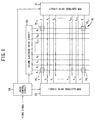
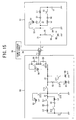
- Fig. 1 is a diagram illustrating an outline configuration of a plasma display device according to the invention.
- the plasma display device is configured of a PDP 50 as a plasma display panel, an X-row electrode drive circuit 51, a Y-row electrode drive circuit 53, a column electrode drive circuit 55, and a drive control circuit 56.
- column electrodes D 1 to D m are extended and arranged in the longitudinal direction (vertical direction) of a two-dimensional display screen, and row electrodes X 1 to X n and row electrodes Y 1 to Y n are extended and arranged in the lateral direction (the horizontal direction) thereof.
- the row electrodes X 1 to X n and row electrodes Y 1 to Y n forms row electrodes pairs (Y 1 , X 1 ), (Y 2 , X 2 ), (Y 3 , X 3 ) ..., (Y n , X n ) which are paired with those adjacent to each other serve as the first display line to the nth display line in the PDP 50.
- a display cell PC which serves as a pixel is formed. More specifically, in the PDP 50, the display cells PC 1,1 to PC 1,m belonging to the first display line, the display cells PC 2,1 to PC 2,m belonging to the second display line, and the display cells PC n,1 to PC n,m belonging to the nth display line are each arranged in a matrix.
- Each of the column electrodes D 1 to D m of the PDP 50 is connected to the column electrode drive circuit 55, each of the row electrodes X 1 to X n is connected to the X-row electrode drive circuit 51, and each of the row electrodes Y 1 to Y n is connected to the Y-row electrode drive circuit 53.
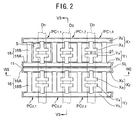
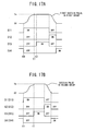
- Fig. 2 is a front view schematically illustrating the internal configuration of the PDF 50 seen from the display surface side.
- Fig. 2 depicts each of the intersection parts of each of the column electrodes D 1 to D 3 with the first display line (Y 1 , X 1 ) and the second display line (Y 2 , X 2 ) in the PDP 50.
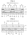
- Fig. 3 depicts a diagram illustrating a cross section of the PDP 50 at a line V3-V3 in Fig. 2
- Fig. 4 depicts a diagram illustrating a cross section of the PDP 50 at a line W2-W2 in Fig. 2.
- each of the row electrodes X is configured of a bus electrode Xb extended in the horizontal direction in the two-dimensional display screen and a T-shaped transparent electrode Xa formed as contacted with the position corresponding to each of the display cells PC on the bus electrode Xb.
- Each of the row electrodes Y is configured of a bus electrode Yb extended in the horizontal direction of the two-dimensional display screen and a T-shaped transparent electrode Ya formed as contacted with the position corresponding to each of the display cells PC on the bus electrode Yb.
- the transparent electrodes Xa and Ya are formed of a transparent conductive film such as ITO, and the bus electrodes Xb and Yb are formed of a metal film, for example. As shown in Fig.
- the front sides thereof are formed on the rear side of a front transparent substrate 10 to be the display surface of the PDP 50.
- the transparent electrodes Xa and Ya in each row electrode pair (X, Y) are extended to the counterpart row electrode side to be paired, and the flat tops of the broad parts are faced to each other through a predetermined width of discharge gap g1.
- a black or dark light absorbing layer (shade layer) 11 extended in the horizontal direction of the two-dimensional display screen is formed between a pair of the row electrode pair (X 1 , Y 1 ) and the row electrode pair (X 2 , Y 2 ) adjacent to this row electrode pair.
- a dielectric layer 12 is formed so as to cover the row electrode pair (X, Y).
- an increased dielectric layer 12A is formed at the portion corresponding to the area where a light absorbing layer 11 and the bus electrodes Xb and Yb adjacent to the light absorbing layer 11 are formed as shown in Fig. 3.
- each of the column electrodes D is formed as extended in the direction orthogonal to the row electrode pair (X, Y) at the position facing the transparent electrodes Xa and Ya in each row electrode pair (X, Y).
- a white column electrode protective layer 15 which covers the column electrode D is further formed.
- partition 16 is formed on the column electrode protective layer 15.
- the partition 16 is formed in a ladder shape of a lateral wall 16A extended in the lateral direction of the two-dimensional display screen at the position corresponding to the bus electrodes Xb and Yb of each row electrode pair (X, Y), and of a vertical wall 16B extended in the longitudinal direction of the two-dimensional display screen at the middle between the column electrodes D adjacent to each other.
- the partition 16 in a ladder shape as shown in Fig. 2 are formed at every display line of the PDF 50, and a space SL exists between the partitions 16 adjacent to each other as shown in Fig. 2.
- the partitions 16 in a ladder shape partition the display cells PC including a discharge Space S, and the transparent electrodes Xa and Ya, each of them is separated.
- a fluorescent material layer 17 is formed so as to cover the entire surfaces thereof as shown in Fig. 3.
- the fluorescent material layer 17 is actually formed of three types of fluorescent materials: a fluorescent material for red light emission, a fluorescent material for green light emission, and a fluorescent material for blue light emission.
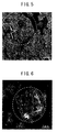
- magnesium oxide crystals forming the magnesium oxide layer 13 contain monocrystals obtained by vapor phase oxidation of magnesium steam that is generated by heating magnesium, such as vapor phase magnesium oxide crystals that are excited by irradiating electron beams to do CL light emission having a peak within a wavelength range of 200 to 300 nm (particularly, near 235 nm within 230 to 250 nm).
- the vapor phase magnesium oxide crystals contain a magnesium monocrystal having a particle diameter of 2000 angstrom or greater with a polycrystal structure in which cubic crystals are fit into each other in a SEM photo image as shown in Fig. 5, or with a cubic monocrystal structure in a SEM photo image as shown in Fig. 6.
- the magnesium monocrystal has features of higher purity, finer particles and less particle coagulation than magnesium oxides generated by other methods have, which contributes to improved discharge properties in discharge delay, etc.
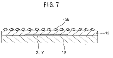
- the vapor phase magnesium oxide monocrystals, which are used have an average particle diameter of 500 angstrom or greater measured by the BET method, preferably 2000 angstrom or greater. Then, as shown in Fig. 7, the magnesium oxide monocrystals are attached to the surface of the dielectric layer 12 by spraying or electrostatic coating to form the magnesium oxide layer 13.
- the magnesium oxide layer 13 may be formed in which a thin magnesium oxide layer is formed on the surface of the dielectric layer 12 and the increased dielectric layer 12A by vapor deposition or sputtering and vapor phase magnesium oxide monocrystals are attached thereon.
- the drive control circuit 56 supplies various control signals that drive the PDP 50 having the structure in accordance with the light emission addressing sequence adopting a subfield method (subframe method) as shown in Fig. 8 to the X-row electrode drive circuit 51, the Y-row electrode drive circuit 53, and the column electrode drive circuit 55.
- the X-row electrode drive circuit 51, the Y-row electrode drive circuit 53, and the column electrode drive circuit 55 generate various drive pulses to be supplied to the PDP 50 in accordance with the light emission addressing sequence as shown in Fig. 8 and supply them to the PDP 50.
- a display period for one field has subfields SF1 to SF12, and the address stage W and the sustain stage I are implanted in each of the subfields SF1 to SF12. Furthermore, only in the starting subfield SF1, a rest stage R is implemented prior to the address stage W.
- the period of the sustain stage I for the subfields SF1 to SF12 is prolonged in order of SF1 to SF12.
- the period where the address stage W is implemented is an address period
- the period where the sustain stage I is implemented is a sustain period.
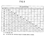
- Fig. 9 depicts a diagram illustrating all the patterns of light emission addressing implemented based on the light emission addressing sequence as shown in Fig. 8. 13 gray scales are formed by the light emission addressing sequence of the subfields SF1 to SF12. As shown in Fig. 9, in the address stage W in one subfield in the subfields SF1 to SF12, selective erasure discharge is implemented for each of the display cells for each of the gray scales (depicted by a black circle). More specifically, wall electric charge formed in all the display cells of the PDP 50 by implementing the reset stage R remains until selective erasure discharge is implemented, and prompts discharge and light emission in the sustain stage I in each subfield SF that exists during that (depicted by a while circle). Each of the display cells becomes in a light emission state while selective erasure discharge is being done for one field period, and 13 gray scales can be obtained by the length of the light emission state.
- Fig. 10 depicts a diagram illustrating the application timing of various drive pulses to be applied to the column electrodes D, and the row electrodes X and Y of the PDP 50, extracting SF1 and SF2 from the subfields SF1 to SF12.
- the X-row electrode drive circuit 51 simultaneously applies a negative reset pulse RP X to the row electrodes X 1 to X n as shown in Fig. 10.
- the reset pulse RP X has a pulse waveform that the voltage value is slowly increased to reach a peak voltage value over time.
- the Y-row electrode drive circuit 53 simultaneously applies to the row electrodes Y 1 to Y n a positive reset pulse RP Y having a waveform that the voltage value is slowly increased to reach a peak voltage value over time as similar to the reset pulse RP X as shown in Fig. 10.
- reset discharge is generated between the row electrodes X and Y in each of all the display cells PC 1,1 to PC n,m .
- a predetermined amount of wall electric charge is formed on the surface of the magnesium oxide layer 13 in the discharge space S in each of the display cells PC. More specifically, it is the state that a so-called wall electric charge is formed in which positive electric charge is formed near the row electrode X and negative electric charge is formed near the row electrode Y on the surface of the magnesium oxide layer 13.
- the discharge probability is significantly improved, the application of a single reset pulse, that is, even a one-time reset discharge allows priming effect to be continued.
- the reset operation and the selective erasure operation can be further stabilized.
- the number of times to do reset discharge is minimized to enhance contrast.
- the Y-row electrode drive circuit 53 applies positive voltages to all the row electrodes Y 1 to Y n , and sequentially applies a scanning pulse SP having a negative voltage to each of the row electrodes Y 1 to Y n . While this is being done, the X-electrode drive circuit 51 changes the potentials of the electrodes X 1 to X n to 0 V.
- the column electrode drive circuit 55 converts each data bit in a pixel drive data bit group DB1 corresponding to the subfield SF1 to a pixel data pulse DP having a pulse voltage corresponding to its logic level.
- the column electrode drive circuit 55 converts the pixel drive data bit of a logic level of 0 to the pixel data pulse DP of a positive high voltage, while converts the pixel drive data bit of a logic level of 1 to the pixel data pulse DP of a low voltage (0 volt). Then, it applies the pixel data pulse DP to the column electrodes D 1 to D m for each display line in synchronization with the application timing of a scanning pulse SP.
- the column electrode drive circuit 55 first applies the pixel data pulse group DP1 formed of m pulses of the pixel data pulses DP corresponding to the first display line to the column electrodes D 1 to D m , and then applies the pixel data pulse group DP2 formed of m pulses of the pixel data pulses DP corresponding to the second display line to the column electrodes D 1 to D m .
- selective erasure discharge is generated to eliminate wall electric charge formed in the display cell PC.
- the selective erasure discharge as above is not generated. Therefore, the state to form wall electric charge is maintained in the display cell PC. More specifically, wall electric charge remains as it is when it exists in the display cell PC, whereas the state not to form wall electric charge is maintained when wall electric charge does not exist.
- selective erasure addressing discharge is selectively generated in each of the display cells PC in accordance with each data bit in the pixel drive data bit group corresponding to the subfield, and then wall electric charge is removed.
- the display cell PC in which wall electric charge remains is set in the lighting state
- the display cell PC in which wall electric charge is removed is set in the unlighted state.
- the X-row electrode drive circuit 51 and the Y-row electrode drive circuit 53 alternately, repeatedly apply positive sustain pulses IP X and IP Y to the row electrodes X 1 to X n and Y 1 to Y n .
- the number of times to apply the sustain pulses IP X and IP Y depends on weighting brightness in each of the subfields.
- the sustain pulses IP X and IP Y are applied, only the display cells PC in the lighting state do sustain discharge, the cells in which a predetermined amount of wall electric charge is formed, and the fluorescent material layer 17 emits light in association with this discharge to form an image on the panel surface.
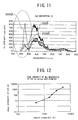
- the vapor phase magnesium monocrystals contained in the magnesium oxide layer 13 formed in each of the display cells PC are excited by irradiating electron beams to do CL light emission having a peak within a wavelength range of 200 to 300 nm (particularly, near 235 nm within 230 to 250 nm) as shown in Fig. 11.
- vapor phase magnesium oxide monocrystals having the average particle diameter of 500 angstrom are formed as well as relatively large monocrystals having the particle diameter of 2000 angstrom or greater as shown in Fig. 5 or Fig. 6. Since temperature to heat magnesium is higher than usual, the length of flame generated by reacting magnesium with oxygen also becomes longer. Thus, the difference between a temperature of the flame and an ambient temperature becomes great, and therefore a group of vapor phase magnesium oxide monocrystals having a greater particle diameter particularly contain many monocrystals of high energy level corresponding to 200 to 300 nm (particularly near 235 nm).
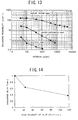
- Fig. 13 is a diagram illustrating discharge probabilities: the discharge probability when no magnesium oxide layer was provided in the display cell PC; the discharge probability when the magnesium oxide layer is constructed by traditional vapor deposition; and the discharge probability when the magnesium oxide layer was provided which contained vapor phase magnesium oxide monocrystals to generate CL light emission having a peak at 200 to 300 nm (particularly near 235 nm within 230 to 250 nm) by irradiating electron beams.
- the horizontal axis is dwell time of discharge, that is, a time interval from discharge being generated to next discharge being generated.
- the magnesium oxide layer 13 which contains the vapor phase magnesium oxide monocrystals that do CL light emission having a peak at 200 to 300 nm (particularly near 235 nm within 230 to 250 nm) by irradiating electron beams as shown in Fig. 5 or Fig. 6 in the discharge space S in each of the display cells PC, the discharge probability is higher than the case where the magnesium oxide layer is formed by traditional vapor deposition.
- those of greater CL light emission intensity having a peak particularly at 235 nm in irradiating electron beams can shorten discharge delay generated in the discharge space S.
- the pulse widths of the pixel data pulse DP and the scanning pulse SP to be applied to the column electrode D and the row electrode Y in order to generate address discharge as shown in Fig. 10 can be shortened. By that amount, processing time for the address stage W can be shortened.
- the pulse width of the sustain pulse IP Y to be applied to the row electrode Y in order to generate sustain discharge as shown in Fig. 10 can be shortened. By that amount, processing time for the sustain stage I can be shortened.
- the number of subfields to be provided in one field (or one frame) display period can be increased, and the number of gray scales can be intended to increase.
- Fig. 15 depicts a specific configuration of the X-row electrode drive circuit 51 and the Y-row electrode drive circuit 53 on electrodes X j and Y j .
- the electrode X j is the electrode at the jth line in electrodes X 1 to X n
- the electrode Y j is the electrode at the jth line in the electrodes Y 1 to Y n .
- the portion between the electrodes X j and Y j serves as a condenser CO.
- the power source B1 outputs a voltage V s (for example, 170 V), and the power source B2 outputs a voltage V r (for example, 190 V).
- V s for example, 170 V
- V r for example, 190 V
- a positive terminal of the power source B1 is connected to a connection line 21 for the electrode X j through a switching element S3, and a negative terminal thereof is grounded.
- a switching element S4 is connected, as well as a series circuit formed of a switching element S1, a diode D1 and a coil L1, and a series circuit formed of a coil L2, a diode D2 and a switching element S2 are connected to the ground side commonly through a condenser C1.
- the diode D1 has an anode on the condenser C1 side, and the diode D2 is connected as the condenser C1 side is a cathode. Furthermore, a positive terminal of the power source B2 is connected to the connection line 21 through a switching element S8 and a resistor R1, and a negative terminal of the power source B2 is grounded.
- the power source B3 outputs a voltage V s (for example, 170 V), the power source B4 outputs a voltage V r (for example, 190 V), the power source B5 outputs a voltage V off (for example, 140 V), and the power source B6 outputs a voltage V h (for example, 160 V, V h > V off ) .
- V s for example, 170 V
- V r for example, 190 V
- V off for example, 140 V
- V a voltage V h for example, 160 V, V h > V off
- a switching element S14 is connected as well as a series circuit formed of a switching element S11, a diode D3 and a coil L3, and a series circuit formed of a coil L4, a diode D4 and a switching element S12 are connected to the ground side commonly through a condenser C2.
- the diode D3 has an anode on the condenser C2 side, and the diode D4 is connected as the condenser C2 side is a cathode.
- connection line 22 is connected to a connection line 23 for the negative terminal of the power source B6 through the switching element S15.
- Positive terminals of the power sources B4 and B5 are grounded, and negative terminals thereof are connected to the connection line 23 through a switching element S16 and a resistor R2.
- the negative terminal of the power source B5 is connected to the connection line 23 through a switching element S17.
- the positive terminal of the power source B6 is connected to a connection line 24 for the electrode Y j through a switching element S21, and the negative terminal of the power source B6 connected to the connection line 23 is connected to the connection line 24 through a switching element S22.
- the diode D5 is connected in parallel to the switching element S21, and the diode D6 is connected in parallel to the switching element S22.
- the diode D5 has an anode on the connection line 24 side, and the diode D6 is connected as the connection line 24 side is a cathode.
- the drive control circuit 56 controls turning on and off the switching elements S1 to S4, S8, S11 to S17, S21 and S22.
- the power source B3, the switching elements S11 to S15, the coils L3 and L4, the diodes D3 and D4, and the condenser C2 configure a sustain driver part
- the power source B4, the resistor R2, and the switching element S16 configure a reset driver part
- the remaining power sources B5 and B6, the switching elements S13, S17, S21, S22, and the diodes D5 and D6 configure a scan driver part.
- the switching element S8 of the X-row electrode drive circuit 51 is turned on, and the switching elements S16 and S22 of the Y-row electrode drive circuit 53 are both turned on. The other switching elements are off. Turning on the switching elements S16 and S22 carries current from the positive terminal of the power source B4 to the electrode Y j through the switching element S16, the resistor R2 and the switching element S22, and turning on the switching element S8 carries current from the electrode X j through the resistor R1, and the switching element S8 to the negative terminal of the power source B2.
- the potential of the electrode X j is gradually decreased by the time constant of the condenser CO and the resistor R1, and is the reset pulse PR X
- the potential of the electrode Y j is gradually increased by the time constant of the condenser CO and the resistor R2, and is the reset pulse PR Y
- the reset pulse PR X finally becomes a voltage -V r
- the reset pulse PR Y finally becomes a voltage V r .
- the reset pulse PR X is applied to all the electrodes X 1 to X n at the same time
- the reset pulse PR Y is generated for each of the electrodes Y 1 to Y n and is applied to all the electrodes Y 1 to Y n .
- the switching elements S8 and S16 are turned off before the reset stage is ended. Furthermore, the switching elements S4, S14 and S15 are turned on at this time, and the electrodes X j and Y j are both grounded. Thus, the reset pulses RP X and RP Y go out.
- the switching elements S14, S15 and S22 are turned off, the switching element S17 is turned on, and the switching element S21 is turned on at the same time.
- the power source B6 is serially connected to the power source B5
- the potential of the positive terminal of the power source B6 is V h - V off .
- the positive potential is applied to the electrode Y j through the switching element S21.
- the column electrode drive circuit 55 converts pixel data for each pixel based on the video signal to the pixel data pulses DP 1 to DP n having a voltage value corresponding to its logic level, and sequentially applies them to the column electrodes D 1 to D m for each one display line.
- the pixel data pulses DP j , DP j-1 with respect to the electrodes Y j , Y j+1 are applied to the column electrode D i .
- the Y-row electrode drive circuit 53 sequentially applies the scanning pulse SP of the negative voltage to the row electrodes Y 1 to Y n in synchronization with the timing of each of the pixel data pulse groups DP 1 to DP n .
- the switching element S21 is turned off, and the switching element S22 is tuned on.
- the negative potential -V off of the negative terminal of the power source B5 is applied to the electrode Y j as the scanning pulse SP through the switching element S17 and the switching element S22.
- the switching element S21 is turned on, the switching element S22 is turned off, and the potential V h - V off of the positive terminal of the power source B6 is applied to the electrode Y j through the switching element S21.
- the scanning pulse SP is applied to the electrode Y j+1 as similar to the electrode Y j in synchronization with the application of the pixel data pulse DP j+1 from the column electrode drive circuit 55.
- the switching elements S17 and S21 are turned off, and the switching elements S14, S15 and S22 are instead turned on.
- the ON-state of the switching element S4 continues.
- the switching element S3 is turned on.
- the potential V s (second potential) of the positive terminal of the power source B1 is applied to the electrode X j , and the potential of the electrode X j is clamped to V s .
- the switching elements S1 and S3 are turned off, the switching element S2 is turned on, and current is carried from the electrode X j into the condenser C1 through the coil L2, the diode D2, and the switching element S2 by electric charge charged in the condenser CO.
- the time constant of the coil L2 and the condenser C1 gradually decreases the potential of the electrode X j as shown in Fig. 16.
- the switching element S2 is turned off, and the switching element S4 is turned on.
- the ON-period of the switching element S3 is the period for the second step.
- the ON-period for the switching element S2 is the period for the third step.
- the X-row electrode drive circuit 51 applies the sustain pulse IP x of the positive voltage to the electrode X j as shown in Fig. 16.
- the switching element S11 is turned on, and the switching element S14 is turned off.
- the potential of the electrode Y j is the ground potential of nearly 0 V when the switching element S14 is on.
- current reaches the electrode Y j through the coil L3, the diode D3, the switching element S11, the switching element S15, and the diode D6 by electric charge charged in the condenser C2 to flow into the condenser CO, and then the condenser CO is charged.
- the time constant of the coil L3 and the condenser CO gradually increases the potential of the electrode Y j as shown in Fig. 16.
- the switching element S13 is turned on.
- the potential V s of the positive terminal of the power source B3 is applied to the electrode Y j through the switching element S13, the switching element S15, and the diode D6.
- the switching elements S11 and S13 are turned off, the switching element S12 is turned on, the switching element S22 is turned on, and current flows from the electrode Y j into the condenser C2 through the switching element S22, the switching element S15, the coil L4, the diode D4, and the switching element S12 by electric charge charged in the condenser CO.
- the time constant of the coil L4 and the condenser C2 gradually decreases the potential of the electrode Y j as shown in Fig. 16.
- the switching elements S12 and S22 are turned off, and the switching element S14 is turned on.
- the Y-row electrode drive circuit 53 it is the period for the first step from when turning on the switching element S11 to right before turning on the switching element S13.
- the ON-period of the switching element S13 is the period for the second step.
- the ON-period of the switching element S12 is the period for third step.
- the Y-row electrode drive circuit 53 applies the sustain pulse IP Y of the positive voltage to the electrode Y j as shown in Fig. 16.
- the sustain pulse IP X and the sustain pulse IP Y are alternately generated and alternately applied to the electrodes X 1 to X n and the electrodes Y 1 to Y n , the display cell in which the wall electric charge still remains repeats discharge light emission to maintain its lighting state.
- the timing to clamp the potential of the sustain pulse IP X (IP Y ) to V s is different between the first group including the beginning first sustain pulse of each of the subfields and the second group after that.
- IP X IP Y
- the switching element S3 is turned on at a time point t2 in the first group, as shown in Fig. 17A, but in the second group, as shown in Fig. 17B, the switching element S3 is turned on at a time point t1 earlier than the time point t2.
- the sustain pulse IP X in the second group is clamped to the potential V s at the time point t1. More specifically, the sustain pulse IP X in the second group is clamped to the potential V s by resonance effect before it reaches the potential V s .
- the sustain pulse IP X in the first group is clamped to the potential V s at the time point t2 delayed from the time point t1.
- the time point t2 is a time after reached to the potential V s of the sustain pulse IP X by resonance effect.
- the second sustain pulse may be generated at a time point for clamping to the potential V s as the first sustain pulse shown in Fig. 17A.
- the sustain pulse IP Y in the Y-row electrode drive circuit 53 is the same, not limited to the X-row electrode drive circuit 51.
- the following may be configured: a rise period of the first sustain pulse in the first group (resonance transition period; t0 to t2) > a rise period of the second sustain pulse in the first group (resonance transition period; t0 to t2') > a rise period of the sustain pulse in the second group (resonance transition period; t0 to t1).
- the rise periods of the first and second sustain pulses are made longer than the rise period of the sustain pulse in the second group in the sustain period of the subfield where three or more of sustain pulses exist to be applied to the sustain period (resonance transition period; t0 to t1) . Namely a time point to be clamped to the second potential is delayed.
- the rise period of the sustain pulse in the first group in the subfield where the number of the sustain pulses to be assigned is small among multiple subfields (a time point to be clamped to the second potential) is made longer (delayed) than the rise period of the sustain pulse in the first group in the subfield where the number of the sustain pulses to be assigned is great (a time point to be clamped to the second potential).
- the time point to be clamped to V s is delayed, that is, the electrode potential is clamped to V s after it reaches V s , and thus ringing of the voltage waveform can be suppressed, and instability of discharge can be suppressed.
- the structure is adopted in which the display cell PC is formed between the row electrodes X and the row electrodes Y that are paired with each other as (X 1 , Y 1 ), (X 2 , Y 2 ) , (X 3 , Y 3 ) , ..., (X n , Y n ).
- the structure may be adopted in which the display cell PC is formed between all the row electrodes.
- the structure may be adopted in which the display cell PC is formed between the row electrodes X 1 and Y 1 , the row electrode Y 1 and X 2 , the row electrode X 2 and Y 2 , ..., the row electrode Y n-1 and X n , the row electrode X n and Y n .
- the structure is adopted in which the row electrodes X and Y are formed in the front transparent substrate 10 and the column electrode D and the fluorescent material layer 17 are formed in the rear substrate 14.
- the structure may be adopted in which the column electrodes D as well as the row electrodes X and Y are formed in the front transparent substrate 10 and the fluorescent material layer 17 is formed in the rear substrate 14.
Landscapes
- Engineering & Computer Science (AREA)
- Physics & Mathematics (AREA)
- Power Engineering (AREA)
- Plasma & Fusion (AREA)
- Computer Hardware Design (AREA)
- General Physics & Mathematics (AREA)
- Theoretical Computer Science (AREA)
- Control Of Indicators Other Than Cathode Ray Tubes (AREA)
- Control Of Gas Discharge Display Tubes (AREA)
- Transforming Electric Information Into Light Information (AREA)
- Gas-Filled Discharge Tubes (AREA)
Applications Claiming Priority (1)
| Application Number | Priority Date | Filing Date | Title |
|---|---|---|---|
| JP2004338724A JP4694823B2 (ja) | 2004-11-24 | 2004-11-24 | プラズマディスプレイ装置 |
Publications (2)
| Publication Number | Publication Date |
|---|---|
| EP1662465A2 true EP1662465A2 (fr) | 2006-05-31 |
| EP1662465A3 EP1662465A3 (fr) | 2008-11-19 |
Family
ID=35976632
Family Applications (1)
| Application Number | Title | Priority Date | Filing Date |
|---|---|---|---|
| EP05024903A Withdrawn EP1662465A3 (fr) | 2004-11-24 | 2005-11-15 | Dispositif d'affichage à plasma |
Country Status (4)
| Country | Link |
|---|---|
| US (1) | US7609232B2 (fr) |
| EP (1) | EP1662465A3 (fr) |
| JP (1) | JP4694823B2 (fr) |
| KR (1) | KR100726934B1 (fr) |
Cited By (2)
| Publication number | Priority date | Publication date | Assignee | Title |
|---|---|---|---|---|
| EP1981016A1 (fr) | 2007-04-09 | 2008-10-15 | Samsung SDI Co., Ltd. | Écran à plasma et dispositif de commande correspondant |
| CN101178868B (zh) * | 2006-11-07 | 2010-06-02 | 三星Sdi株式会社 | 等离子体显示装置及其驱动方法 |
Families Citing this family (8)
| Publication number | Priority date | Publication date | Assignee | Title |
|---|---|---|---|---|
| JP4704109B2 (ja) * | 2005-05-30 | 2011-06-15 | パナソニック株式会社 | プラズマディスプレイ装置 |
| JP4987255B2 (ja) * | 2005-06-22 | 2012-07-25 | パナソニック株式会社 | プラズマディスプレイ装置 |
| JP4976684B2 (ja) * | 2005-11-04 | 2012-07-18 | パナソニック株式会社 | プラズマディスプレイ装置 |
| CN101136165A (zh) | 2006-10-12 | 2008-03-05 | 乐金电子(南京)等离子有限公司 | 等离子显示装置 |
| JPWO2009063624A1 (ja) | 2007-11-15 | 2011-03-31 | パナソニック株式会社 | プラズマディスプレイ装置およびプラズマディスプレイパネルの駆動方法 |
| KR101067165B1 (ko) | 2007-11-15 | 2011-09-22 | 파나소닉 주식회사 | 플라즈마 디스플레이 장치 및 플라즈마 디스플레이 패널의 구동 방법 |
| JP2009259671A (ja) * | 2008-04-18 | 2009-11-05 | Panasonic Corp | プラズマディスプレイ装置 |
| KR102389482B1 (ko) | 2017-12-04 | 2022-04-21 | 삼성전자주식회사 | 이미지 센서 패키지 및 이미지 센싱 모듈 |
Citations (4)
| Publication number | Priority date | Publication date | Assignee | Title |
|---|---|---|---|---|
| JPH07192630A (ja) * | 1993-12-27 | 1995-07-28 | Oki Electric Ind Co Ltd | ガス放電表示パネル及びその保護膜形成方法 |
| EP1152387A1 (fr) * | 1999-11-12 | 2001-11-07 | Matsushita Electric Industrial Co., Ltd. | Ecran et son procede de commande |
| US20020054002A1 (en) * | 2000-05-25 | 2002-05-09 | Pioneer Corporation | Method for driving a plasma display panel |
| WO2004055771A1 (fr) * | 2002-12-13 | 2004-07-01 | Matsushita Electric Industrial Co., Ltd. | Procede d'activation d'un panneau d'affichage plasma |
Family Cites Families (13)
| Publication number | Priority date | Publication date | Assignee | Title |
|---|---|---|---|---|
| JPH08152864A (ja) * | 1994-11-29 | 1996-06-11 | Oki Electric Ind Co Ltd | Ac型ガス放電パネルの駆動方法 |
| JPH0934397A (ja) * | 1995-07-24 | 1997-02-07 | Fujitsu Ltd | プラズマ・ディスプレイ・パネル |
| JP3630290B2 (ja) * | 1998-09-28 | 2005-03-16 | パイオニアプラズマディスプレイ株式会社 | プラズマディスプレイパネルの駆動方法およびプラズマディスプレイ |
| JP2001228823A (ja) * | 1999-12-07 | 2001-08-24 | Pioneer Electronic Corp | プラズマディスプレイ装置 |
| JP3512075B2 (ja) * | 2000-03-23 | 2004-03-29 | 日本電気株式会社 | プラズマディスプレイパネルの駆動方法 |
| WO2002019368A1 (fr) * | 2000-08-29 | 2002-03-07 | Matsushita Electric Industrial Co., Ltd. | Ecran a plasma et son procede de production et unite d'affichage d'ecran a plasma |
| JP2004045704A (ja) * | 2002-07-11 | 2004-02-12 | Matsushita Electric Ind Co Ltd | プラズマディスプレイの駆動方法および駆動装置 |
| KR100484175B1 (ko) * | 2002-11-08 | 2005-04-18 | 삼성전자주식회사 | 고효율 플라즈마 디스플레이 패널 구동 장치 및 방법 |
| JP4100338B2 (ja) * | 2002-12-13 | 2008-06-11 | 松下電器産業株式会社 | プラズマディスプレイパネルの駆動方法 |
| JP4541832B2 (ja) * | 2004-03-19 | 2010-09-08 | パナソニック株式会社 | プラズマディスプレイパネル |
| JP4541108B2 (ja) * | 2004-04-26 | 2010-09-08 | パナソニック株式会社 | プラズマディスプレイ装置 |
| JP4481131B2 (ja) * | 2004-05-25 | 2010-06-16 | パナソニック株式会社 | プラズマディスプレイ装置 |
| JP4704109B2 (ja) * | 2005-05-30 | 2011-06-15 | パナソニック株式会社 | プラズマディスプレイ装置 |
-
2004
- 2004-11-24 JP JP2004338724A patent/JP4694823B2/ja not_active Expired - Fee Related
-
2005
- 2005-11-15 EP EP05024903A patent/EP1662465A3/fr not_active Withdrawn
- 2005-11-17 US US11/280,271 patent/US7609232B2/en not_active Expired - Fee Related
- 2005-11-24 KR KR1020050112787A patent/KR100726934B1/ko not_active IP Right Cessation
Patent Citations (4)
| Publication number | Priority date | Publication date | Assignee | Title |
|---|---|---|---|---|
| JPH07192630A (ja) * | 1993-12-27 | 1995-07-28 | Oki Electric Ind Co Ltd | ガス放電表示パネル及びその保護膜形成方法 |
| EP1152387A1 (fr) * | 1999-11-12 | 2001-11-07 | Matsushita Electric Industrial Co., Ltd. | Ecran et son procede de commande |
| US20020054002A1 (en) * | 2000-05-25 | 2002-05-09 | Pioneer Corporation | Method for driving a plasma display panel |
| WO2004055771A1 (fr) * | 2002-12-13 | 2004-07-01 | Matsushita Electric Industrial Co., Ltd. | Procede d'activation d'un panneau d'affichage plasma |
Cited By (3)
| Publication number | Priority date | Publication date | Assignee | Title |
|---|---|---|---|---|
| CN101178868B (zh) * | 2006-11-07 | 2010-06-02 | 三星Sdi株式会社 | 等离子体显示装置及其驱动方法 |
| US7978155B2 (en) | 2006-11-07 | 2011-07-12 | Samsung Sdi Co., Ltd. | Plasma display device and driving method thereof |
| EP1981016A1 (fr) | 2007-04-09 | 2008-10-15 | Samsung SDI Co., Ltd. | Écran à plasma et dispositif de commande correspondant |
Also Published As
| Publication number | Publication date |
|---|---|
| KR20060058038A (ko) | 2006-05-29 |
| JP2006146035A (ja) | 2006-06-08 |
| US20060109210A1 (en) | 2006-05-25 |
| JP4694823B2 (ja) | 2011-06-08 |
| EP1662465A3 (fr) | 2008-11-19 |
| US7609232B2 (en) | 2009-10-27 |
| KR100726934B1 (ko) | 2007-06-14 |
Similar Documents
| Publication | Publication Date | Title |
|---|---|---|
| US7852296B2 (en) | Plasma display device | |
| US7965259B2 (en) | Plasma display device | |
| US7609232B2 (en) | Plasma display device | |
| US7834820B2 (en) | Plasma display device | |
| US7742018B2 (en) | Plasma display device | |
| EP1763001A2 (fr) | Dispositif d'affichage à plasma | |
| US7777695B2 (en) | Plasma display device | |
| US7724213B2 (en) | Plasma display device | |
| US7786957B2 (en) | Plasma display device | |
| US20080074354A1 (en) | Plasma display apparatus | |
| JP5110838B2 (ja) | プラズマディスプレイ装置 | |
| WO2003015068A1 (fr) | Procede pour piloter un ecran d'affichage a plasma de type a ca | |
| JP2010008583A (ja) | プラズマディスプレイパネルの駆動方法 |
Legal Events
| Date | Code | Title | Description |
|---|---|---|---|
| PUAI | Public reference made under article 153(3) epc to a published international application that has entered the european phase |
Free format text: ORIGINAL CODE: 0009012 |
|
| AK | Designated contracting states |
Kind code of ref document: A2 Designated state(s): AT BE BG CH CY CZ DE DK EE ES FI FR GB GR HU IE IS IT LI LT LU LV MC NL PL PT RO SE SI SK TR |
|
| AX | Request for extension of the european patent |
Extension state: AL BA HR MK YU |
|
| PUAL | Search report despatched |
Free format text: ORIGINAL CODE: 0009013 |
|
| AK | Designated contracting states |
Kind code of ref document: A3 Designated state(s): AT BE BG CH CY CZ DE DK EE ES FI FR GB GR HU IE IS IT LI LT LU LV MC NL PL PT RO SE SI SK TR |
|
| AX | Request for extension of the european patent |
Extension state: AL BA HR MK YU |
|
| 17P | Request for examination filed |
Effective date: 20081114 |
|
| 17Q | First examination report despatched |
Effective date: 20090108 |
|
| AKX | Designation fees paid |
Designated state(s): DE FR GB |
|
| RAP1 | Party data changed (applicant data changed or rights of an application transferred) |
Owner name: PANASONIC CORPORATION |
|
| STAA | Information on the status of an ep patent application or granted ep patent |
Free format text: STATUS: THE APPLICATION IS DEEMED TO BE WITHDRAWN |
|
| 18D | Application deemed to be withdrawn |
Effective date: 20120601 |