EP1662327A2 - Table pour substrat, méthode de mesure de position de substrat et appareil lithographique - Google Patents
Table pour substrat, méthode de mesure de position de substrat et appareil lithographique Download PDFInfo
- Publication number
- EP1662327A2 EP1662327A2 EP05110761A EP05110761A EP1662327A2 EP 1662327 A2 EP1662327 A2 EP 1662327A2 EP 05110761 A EP05110761 A EP 05110761A EP 05110761 A EP05110761 A EP 05110761A EP 1662327 A2 EP1662327 A2 EP 1662327A2
- Authority
- EP
- European Patent Office
- Prior art keywords
- substrate
- alignment
- optical
- grating
- mark
- Prior art date
- Legal status (The legal status is an assumption and is not a legal conclusion. Google has not performed a legal analysis and makes no representation as to the accuracy of the status listed.)
- Withdrawn
Links
Images


Classifications
-
- G—PHYSICS
- G03—PHOTOGRAPHY; CINEMATOGRAPHY; ANALOGOUS TECHNIQUES USING WAVES OTHER THAN OPTICAL WAVES; ELECTROGRAPHY; HOLOGRAPHY
- G03F—PHOTOMECHANICAL PRODUCTION OF TEXTURED OR PATTERNED SURFACES, e.g. FOR PRINTING, FOR PROCESSING OF SEMICONDUCTOR DEVICES; MATERIALS THEREFOR; ORIGINALS THEREFOR; APPARATUS SPECIALLY ADAPTED THEREFOR
- G03F9/00—Registration or positioning of originals, masks, frames, photographic sheets or textured or patterned surfaces, e.g. automatically
- G03F9/70—Registration or positioning of originals, masks, frames, photographic sheets or textured or patterned surfaces, e.g. automatically for microlithography
- G03F9/7088—Alignment mark detection, e.g. TTR, TTL, off-axis detection, array detector, video detection
-
- G—PHYSICS
- G03—PHOTOGRAPHY; CINEMATOGRAPHY; ANALOGOUS TECHNIQUES USING WAVES OTHER THAN OPTICAL WAVES; ELECTROGRAPHY; HOLOGRAPHY
- G03F—PHOTOMECHANICAL PRODUCTION OF TEXTURED OR PATTERNED SURFACES, e.g. FOR PRINTING, FOR PROCESSING OF SEMICONDUCTOR DEVICES; MATERIALS THEREFOR; ORIGINALS THEREFOR; APPARATUS SPECIALLY ADAPTED THEREFOR
- G03F7/00—Photomechanical, e.g. photolithographic, production of textured or patterned surfaces, e.g. printing surfaces; Materials therefor, e.g. comprising photoresists; Apparatus specially adapted therefor
- G03F7/70—Microphotolithographic exposure; Apparatus therefor
- G03F7/70691—Handling of masks or workpieces
- G03F7/70716—Stages
-
- G—PHYSICS
- G03—PHOTOGRAPHY; CINEMATOGRAPHY; ANALOGOUS TECHNIQUES USING WAVES OTHER THAN OPTICAL WAVES; ELECTROGRAPHY; HOLOGRAPHY
- G03F—PHOTOMECHANICAL PRODUCTION OF TEXTURED OR PATTERNED SURFACES, e.g. FOR PRINTING, FOR PROCESSING OF SEMICONDUCTOR DEVICES; MATERIALS THEREFOR; ORIGINALS THEREFOR; APPARATUS SPECIALLY ADAPTED THEREFOR
- G03F9/00—Registration or positioning of originals, masks, frames, photographic sheets or textured or patterned surfaces, e.g. automatically
- G03F9/70—Registration or positioning of originals, masks, frames, photographic sheets or textured or patterned surfaces, e.g. automatically for microlithography
- G03F9/7003—Alignment type or strategy, e.g. leveling, global alignment
- G03F9/7007—Alignment other than original with workpiece
- G03F9/7011—Pre-exposure scan; original with original holder alignment; Prealignment, i.e. workpiece with workpiece holder
-
- G—PHYSICS
- G03—PHOTOGRAPHY; CINEMATOGRAPHY; ANALOGOUS TECHNIQUES USING WAVES OTHER THAN OPTICAL WAVES; ELECTROGRAPHY; HOLOGRAPHY
- G03F—PHOTOMECHANICAL PRODUCTION OF TEXTURED OR PATTERNED SURFACES, e.g. FOR PRINTING, FOR PROCESSING OF SEMICONDUCTOR DEVICES; MATERIALS THEREFOR; ORIGINALS THEREFOR; APPARATUS SPECIALLY ADAPTED THEREFOR
- G03F9/00—Registration or positioning of originals, masks, frames, photographic sheets or textured or patterned surfaces, e.g. automatically
- G03F9/70—Registration or positioning of originals, masks, frames, photographic sheets or textured or patterned surfaces, e.g. automatically for microlithography
- G03F9/7049—Technique, e.g. interferometric
-
- G—PHYSICS
- G03—PHOTOGRAPHY; CINEMATOGRAPHY; ANALOGOUS TECHNIQUES USING WAVES OTHER THAN OPTICAL WAVES; ELECTROGRAPHY; HOLOGRAPHY
- G03F—PHOTOMECHANICAL PRODUCTION OF TEXTURED OR PATTERNED SURFACES, e.g. FOR PRINTING, FOR PROCESSING OF SEMICONDUCTOR DEVICES; MATERIALS THEREFOR; ORIGINALS THEREFOR; APPARATUS SPECIALLY ADAPTED THEREFOR
- G03F9/00—Registration or positioning of originals, masks, frames, photographic sheets or textured or patterned surfaces, e.g. automatically
- G03F9/70—Registration or positioning of originals, masks, frames, photographic sheets or textured or patterned surfaces, e.g. automatically for microlithography
- G03F9/7073—Alignment marks and their environment
- G03F9/7084—Position of mark on substrate, i.e. position in (x, y, z) of mark, e.g. buried or resist covered mark, mark on rearside, at the substrate edge, in the circuit area, latent image mark, marks in plural levels
Definitions
- the present invention relates to a substrate table arranged to support a substrate provided with at least one substrate mark, the at least one substrate mark having a position that can be measured using an alignment system.
- the present invention further relates to a method of measuring a position of a substrate on the substrate table.
- a lithographic apparatus is a machine that applies a desired pattern onto a substrate, usually onto a target portion of the substrate.
- a lithographic apparatus can be used, for example, in the manufacture of integrated circuits (ICs).
- a patterning device which is alternatively referred to as a mask or a reticle, may be used to generate a circuit pattern to be formed on an individual layer of the IC.
- This pattern can be transferred onto a target portion (e.g. comprising part of, one, or several dies) on a substrate (e.g. a silicon wafer). Transfer of the pattern is typically via imaging onto a layer of radiation-sensitive material (resist) provided on the substrate.
- resist radiation-sensitive material
- a single substrate will contain a network of adjacent target portions that are successively patterned.
- lithographic apparatus include so-called steppers, in which each target portion is irradiated by exposing an entire pattern onto the target portion at one time, and so-called scanners, in which each target portion is irradiated by scanning the pattern through a radiation beam in a given direction (the "scanning"-direction) while synchronously scanning the substrate parallel or anti-parallel to this direction. It is also possible to transfer the pattern from the patterning device to the substrate by imprinting the pattern onto the substrate.
- lithographic apparatus in the manufacture of ICs, it should be understood that the lithographic apparatus described herein may have other applications, such as the manufacture of integrated optical systems, guidance and detection patterns for magnetic domain memories, flatpanel displays, liquid-crystal displays (LCDs), thin-film magnetic heads, etc.
- LCDs liquid-crystal displays
- any use of the terms “wafer” or “die” herein may be considered as synonymous with the more general terms “substrate” or “target portion”, respectively.
- the substrate referred to herein may be processed, before or after exposure, in for example a track (a tool that typically applies a layer of resist to a substrate and develops the exposed resist), a metrology tool and/or an inspection tool.
- the disclosure herein may be applied to such and other substrate processing tools.
- the substrate may be processed more than once, for example in order to create a multilayer IC, so that the term substrate used herein may also refer to a substrate that already contains multiple processed layers.
- imprint lithography a topography in a patterning device defines the pattern created on a substrate.
- the topography of the patterning device may be pressed into a layer of resist supplied to the substrate whereupon the resist is cured by applying electromagnetic radiation, heat, pressure or a combination thereof
- the patterning device is moved out of the resist leaving a pattern in it after the resist is cured.
- UV radiation e.g. having a wavelength of or about 436, 365, 355, 248, 193, 157 or 126 nm
- EUV radiation e.g. having a wavelength in the range of 5-20 nm
- particle beams such as ion beams or electron beams.
- lens may refer to any one or combination of various types of optical components, including refractive, reflective, magnetic, electromagnetic and electrostatic optical components.
- Alignment is the process of positioning the image of a specific point on the mask to a specific point on the substrate that is to be exposed.
- one or more alignment marks such as a small pattern, are provided on each of the substrate and the mask.
- a device may comprise many layers that are built up by successive exposures with intermediate processing steps. Before each exposure, alignment is performed to minimize any positional error between the new exposure and the previous ones, such error being termed overlay error.
- CMP chemical mechanical polishing
- rapid thermal annealing rapid thermal annealing
- thick layer deposition thick layer deposition
- deep trench etching can damage or distort the alignment marks on the substrate or bury them under opaque layers.
- the alignment marks are not clearly visible or not visible at all, negatively influencing the accuracy of alignment. This can cause overlay errors.
- MST micro systems technology
- MEMS micro electro-mechanical systems
- New techniques are developed that allow the imaging of patterning features having even smaller patterns by using so-called immersion techniques.
- This technique is based on the fact that the space between the lens and the substrate is filled with a fluid, such as water. Since the refractive index of water is higher than the refractive index of air of some low pressure gas, the numerical aperture of the system is increased. This allows the system to image even smaller patterns, while using the same radiation system and projection system. More information about immersion techniques may be found in EP 1 420 298 A2, EP 1 429 188 and EP 1 420 300 A2. The presence of water may, however, influence the alignment measurements. As a result of the presence of water in the space between the lens and the substrate, it becomes difficult to perform alignment measurements on marks provided on the substrate. Furthermore, comparing such 'wet' measurements with previously obtained 'dry' alignment measurements is also rather difficult.
- the conventional alignment techniques are all performed on the top side of the substrate, i.e. at the side at which the exposure is performed. This side will be referred to as the first side or the front side of the substrate.
- Such alignment techniques all measure the position of the substrate by measuring the position of alignment marks provided on the top side of the substrate.
- these conventional alignment techniques are difficult to perform and are less accurate.
- Conventional alignment techniques typically use optical measurement techniques that measure the position of alignment marks provided on the top side of the substrate, i.e. the side of the substrate that does not face the substrate table on which the substrate is positioned. This makes it difficult to use these alignment techniques in combination with devices fabricated from both sides since, in that case, a substrate needs to be positioned such that the alignment marks face the substrate table.
- the optics of the alignment system are usually positioned outside the area filled with liquid, so the optics and/or the optical signals need to be guided into the liquid. This is not an easy task and requires complicated and expensive techniques.
- alignment techniques that are arranged to measure the position of an alignment mark provided on the back-side of the substrate, i.e. the side of the substrate facing the substrate table and the side that is not exposed. This side will also be referred to as the second side of the substrate.
- the second side faces the substrate table that supports the substrate.
- optical devices are provided in the substrate table. This technique is generally referred to as backside alignment and will be discussed in more detail below. A more extensive description can be found in US 2002/0109825 A1, owned by ASML.
- the perception at this moment is that alignment measurements via the second side of the substrate using the optical devices provided in the substrate table may be less accurate than alignment measurements based on alignment markers provided on the first side of the substrate that can be measured directly. Therefore, improvements of backside alignment techniques are needed.
- reference to an alignment mark being located on a particular side of the substrate includes the alignment mark being etched into a respective side of the substrate and includes having subsequent material deposited on top of the alignment mark such that it is embedded and is no longer necessarily exposed at the surface.
- the apparatus may be employed in the manufacture of integrated optical systems, guidance and detection patterns for magnetic domain memories, liquid-crystal display panels, thin-film magnetic heads, etc.
- a device for generating at least one virtual substrate mark comprising a substrate table that is arranged to support a substrate having at least one substrate mark, an optical system that is associated with the substrate table, the optical system having one or more optical arms comprising at least two mirrors arranged to reflect radiation, and at least two lenses positioned to receive radiation reflected from the mirrors, the lenses providing a magnification factor deviating from one, wherein the one or more optical arms generate the at least one virtual substrate mark from a corresponding at least one substrate mark.
- a method of measuring a position of a substrate provided on a substrate table, the substrate having a plurality of substrate marks thereon with at least two of the substrate marks being of different sizes comprises creating a first virtual substrate mark corresponding to a substrate mark having a first size, the first virtual substrate mark being created using a first magnification factor, creating a second virtual substrate mark corresponding to a substrate mark having a second size, the second virtual substrate mark being created using a second magnification factor, and determining a first alignment position for the first virtual substrate mark.
- an apparatus for generating a Moiré pattern comprising a substrate table that is arranged to support a substrate having at least one substrate alignment grating, and a window provided with an alignment grating, wherein the window alignment grating is configured such that when the substrate is supported by the substrate table, the substrate alignment grating and the window alignment grating together form a Moiré pattern which may be used by an alignment system to determine the position of the substrate.
- a method of measuring a position of a substrate provided on a substrate table comprising providing the substrate at a location such that an alignment grating provided on the substrate and an alignment grating provided on a window in the substrate table will together form a Moiré pattern, forming an image of the Moiré pattern using optics located in the substrate table, then measuring the location of the image of the Moiré pattern using an alignment system.
- a method of measuring a position of a substrate provided on a substrate table comprising providing the substrate at a location such that an alignment grating provided on the substrate and an alignment grating provided on a window in an alignment system will together form a Moiré pattern, then measuring the location of the Moiré pattern using the alignment system.
- Figure 1 illustrates a lithographic apparatus according to an embodiment of the invention
- Figure 2 is a schematic cross section illustrating the substrate table incorporating two branches of an optical system for double side alignment
- Figure 3 is a plan view of a substrate showing the position and orientation of the double side alignment optics
- Figure 4 is plan view showing an alternative position and orientation of the double side alignment optics
- Figure 5 is a cross section of a portion of a substrate table having integral optical components
- Figure 6 is a cross section of a portion of a substrate table having integral optical components according to the invention.
- Figure 7 is a top view of a portion of a substrate table having integral optical components according to a further embodiment of the invention.
- Figure 8 depicts a mark that may be used in an embodiment according to the invention.
- Figure 9 is a cross sectional view of an alternative embodiment of the invention.
- Figure 10 is a schematic diagram which illustrates the operation of the alternative embodiment of the invention.
- Figure 11 is a plan view of part of the apparatus shown in figure 9.
- Figure 12 is a side vie of an implementation of the alternative embodiment of the invention.
- Figure 1 schematically depicts a lithographic apparatus according to one embodiment of the invention.
- the apparatus comprises:
- the illumination system may include various types of optical components, such as refractive, reflective, magnetic, electromagnetic, electrostatic or other types of optical components, or any combination thereof, for directing, shaping, or controlling radiation.
- optical components such as refractive, reflective, magnetic, electromagnetic, electrostatic or other types of optical components, or any combination thereof, for directing, shaping, or controlling radiation.
- the support structure supports, i.e. bears the weight of, the patterning device. It holds the patterning device in a manner that depends on the orientation of the patterning device, the design of the lithographic apparatus, and other conditions, such as, for example, whether or not the patterning device is held in a vacuum environment.
- the support structure can use mechanical, vacuum, electrostatic or other clamping techniques to hold the patterning device.
- the support structure may be a frame or a table, for example, which may be fixed or movable as required.
- the support structure may ensure that the patterning device is at a desired position, for example, with respect to the projection system. Any use of the terms "reticle” or “mask” herein may be considered synonymous with the more general term "patterning device.”
- patterning device used herein should be broadly interpreted as referring to any device that can be used to impart a radiation beam with a pattern in its cross-section such as to create a pattern in a target portion of the substrate. It should be noted that the pattern imparted to the radiation beam may not exactly correspond to the desired pattern in the target portion of the substrate, for example, if the pattern includes phase-shifting features or so called assist features. Generally, the pattern imparted to the radiation beam will correspond to a particular functional layer in a device being created in the target portion, such as an integrated circuit.
- the patterning device may be transmissive or reflective.
- Examples of patterning devices include masks, programmable mirror arrays, and programmable LCD panels.
- Masks are well known in lithography, and include mask types such as binary, alternating phase-shift, and attenuated phase-shift, as well as various hybrid mask types.
- An example of a programmable mirror array employs a matrix arrangement of small mirrors, each of which can be individually tilted so as to reflect an incoming radiation beam in different directions. The tilted mirrors impart a pattern in a radiation beam which is reflected by the mirror matrix.
- projection system used herein should be broadly interpreted as encompassing any type of projection system, including refractive, reflective, catadioptric, magnetic, electromagnetic and electrostatic optical systems, or any combination thereof, as appropriate for the exposure radiation being used, or for other factors such as the use of an immersion liquid or the use of a vacuum. Any use of the term “projection lens” herein may be considered as synonymous with the more general term “projection system”.
- the apparatus is of a transmissive type (e.g. employing a transmissive mask).
- the apparatus may be of a reflective type (e.g. employing a programmable mirror array or employing a reflective mask).
- the lithographic apparatus may be of a type having two (dual stage) or more substrate tables (and/or two or more mask tables). In such "multiple stage” machines the additional tables may be used in parallel, or preparatory steps may be carried out on one or more tables while one or more other tables are being used for exposure.
- the lithographic apparatus may also be of a type wherein at least a portion of the substrate may be covered by a liquid having a relatively high refractive index, e.g. water, so as to fill a space between the projection system and the substrate.
- a liquid having a relatively high refractive index e.g. water
- An immersion liquid may also be applied to other spaces in the lithographic apparatus, for example, between the mask and the projection system. Immersion techniques are well known in the art for increasing the numerical aperture of projection systems.
- immersion as used herein does not mean that a structure, such as a substrate, must be submerged in liquid, but rather means that liquid is located between the projection system and the substrate during exposure.
- the illuminator IL receives a radiation beam from a radiation source SO.
- the source and the lithographic apparatus may be separate entities, for example when the source is an excimer laser. In such cases, the source is not considered to form part of the lithographic apparatus and the radiation beam is passed from the source SO to the illuminator IL with the aid of a beam delivery system BD comprising, for example, suitable directing mirrors and/or a beam expander. In other cases the source may be an integral part of the lithographic apparatus, for example when the source is a mercury lamp.
- the source SO and the illuminator IL, together with the beam delivery system BD if required, may be referred to as a radiation system.
- the illuminator IL may comprise an adjuster AD for adjusting the angular intensity distribution of the radiation beam.
- an adjuster AD for adjusting the angular intensity distribution of the radiation beam.
- at least the outer and/or inner radial extent (commonly referred to as ⁇ -outer and ⁇ -inner, respectively) of the intensity distribution in a pupil plane of the illuminator may be adjusted.
- the illuminator IL may comprise various other components, such as an integrator IN and a condenser CO.
- the illuminator may be used to condition the radiation beam, to have a desired uniformity and intensity distribution in its cross-section.
- the radiation beam B is incident on the patterning device (e.g., mask MA), which is held on the support structure (e.g., mask table MT), and is patterned by the patterning device. Having traversed the mask MA, the radiation beam B passes through the projection system PS, which focuses the beam onto a target portion C of the substrate W.
- the substrate table WT can be moved accurately, e.g. so as to position different target portions C in the path of the radiation beam B.
- the first positioner PM and another position sensor may be used to accurately position the mask MA with respect to the path of the radiation beam B, e.g. after mechanical retrieval from a mask library, or during a scan.
- movement of the mask table MT may be realized with the aid of a long-stroke module (coarse positioning) and a short-stroke module (fine positioning), which form part of the first positioner PM.
- movement of the substrate table WT may be realized using a long-stroke module and a short-stroke module, which form part of the second positioner PW.
- the mask table MT may be connected to a short-stroke actuator only, or may be fixed.
- Mask MA and substrate W may be aligned using mask alignment marks M1, M2 and substrate alignment marks PI, P2.
- the substrate alignment marks as illustrated, occupy dedicated target portions, they may be located in spaces between target portions (these are known as scribe-lane alignment marks).
- the mask alignment marks may be located between the dies.
- the depicted apparatus could be used in at least one of the following modes:
- FIG. 2 shows a substrate W on a substrate table WT.
- Substrate marks WM3 and WM4 are provided on a first side ("front side") of the substrate W and light may be reflected from these marks, as indicated by the arrows above WM3 and WM4, and used for alignment with marks on a mask in conjunction with an alignment system (not shown).
- a more detailed description of this is disclosed in US patent application number 10/736, 911, filed 17 December 2003, which is hereby incorporated by reference in its entirety.
- substrate marks WM1 and WM2 are provided on a second side ("back side") of the substrate W.
- An optical system is built into the substrate table WT for providing optical access to the substrate marks WM1, WM2 on the back side of the substrate W.
- the optical system comprises a pair of arms 10a, 10b. Each arm consists of two mirrors, 12, 14 and two lenses 16, 18.
- the mirrors 12, 14 in each arm are inclined such that the sum of the angles that they make with the horizontal is 90°. In this way, a beam of light impinging vertically on one of the mirrors will remain vertical when reflected off the other mirror.
- the lenses and the mounting may be designed in such a way that they may take account of a large part of the direction change, as long as the total of the optical system provides a direction change of 180°.
- light is directed from above the substrate table WT onto mirror 12, through lenses 16 and 18, onto mirror 14 and then onto the respective substrate mark WM1, WM2.
- Light is reflected off portions of the substrate mark and returns along the arm of the optical system via mirror 14, lenses 18 and 16 and mirror 12.
- the mirrors 12, 14 and lenses 16, 18 are arranged such that an image 20a, 20b20a, 20b of the substrate mark WM1, WM2 is formed at the plane of the front (top) surface of the substrate W, corresponding to the vertical position of any substrate marks WM3, WM4 provided on the front side of the substrate W.
- the order of the lenses 16, 18 and the mirrors 12, 14 may be different, as appropriate to the optical system.
- lens 18 may be between the mirror 14 and the substrate W (see illustrations of later embodiments).
- Image 20a, 20b of substrate mark WM1, WM2 acts as a virtual substrate mark and may be used for alignment by the pre-existing alignment system (not shown) in exactly the same way as a real substrate mark provided on the front (top) side of the substrate W.
- the arms of the optical system 10a, 10b produce images 20a, 20b which are displaced to the side of the substrate W so that they may be viewed by an alignment system above the substrate W.
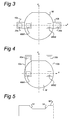
- Two preferred orientations of the arms of the optical system 10a, 10b are shown in Figures 3 and 4, which are plan views of the substrate W, which lies in the XY plane.
- the substrate table WT is omitted from Figures 3 and 4 for clarity.
- the arms of the optical system 10a, 10b are aligned along the X axis.
- the arms of the optical system 10a, 10b are parallel to the Y axis. In both cases, the substrate marks WM1, WM2 lie on the X axis.
- the substrate marks WM1, WM2 are located on the underside of the substrate W, so they are reversed from the point of view of the top side of the substrate W.
- the arrangement of the mirrors 12, 14 of the arms of the optical system may be configured so that the images 20a, 20b of the substrate marks WM1, WM2 are restored proper orientation.
- the optical system also may be arranged so that the ratio of the size of a substrate mark WM1, WM2 to its image 20a, 20b is 1:1 i.e. there is no magnification or reduction. Consequently, the images 20a, 20b can be used exactly as if they were real substrate marks on the front side of the substrate W.
- a common alignment pattern or key provided on a mask may be used to perform alignment with both real and virtual substrate marks.
- substrate marks are provided on both the front and back sides of the substrate W at corresponding positions, as shown in Figure 2.
- Figures 3 and 4 only the substrate marks on the back side of the substrate W are shown, for clarity.
- a substrate mark that was on the top side of the substrate W now may be on the underside of the substrate W, but at a position such that it may be imaged by an arm of the optical system 10a, 10b.
- a substrate table WT may be provided with a mirror arrangement that does not change the direction of movement of the images 20a, 20b with respect to the movement of the substrate marks WM1, WM2.
- At least two substrate marks may be provided per side of the substrate W.
- a single mark may provide information about the relative positioning of an image of a specific point on a mask to a specific point on the substrate. However, to ensure the correct orientational alignment and magnification, at least two marks may be used.
- Figure 5 shows a portion of the substrate table WT in cross section.
- the optical system 10a, 10b for imaging the substrate marks on the back side of a substrate may be built into the substrate table WT in a particular fashion.
- the mirrors 12, 14 of an arm of the optical system may not be provided as discrete components, but are integral with the substrate table WT.
- Appropriate faces are machined into the substrate table WT, which may then be provided with a coating to improve reflectivity, thus forming the mirrors 12, 14.
- the optical system may be made from the same material as the substrate table, such a Zerodur TM , which has a very low coefficient of thermal expansion and therefore ensures that high alignment accuracy can be maintained.
- the substrate marks WM1, WM2, WM3, WM4 may be provided on the substrate W in order to allow alignment of the substrate W with respect to the projected patterned beam. Alignment is necessary to allow optimal positioning of different layers of the substrate W with respect to each other.
- a substrate W may be built up from a plurality of layers that are each formed on the substrate W one after the other and are subject to an exposure. Since the different layers are configured to form a working device, the different exposures should be optimally aligned with respect to each other.
- integrated circuits are made in layers.
- Each layer may start with the exposure of a (different) pattern on the substrate W. This pattern may need to fit optimally on the previous one.
- a measure for accomplished accuracy in this alignment is overlay O.
- a formula may be derived to describe a relationship between the position of the substrate marks WM3, WM4 on the substrate W and the overlay O in case a conventional alignment technique is used, i.e. the substrate marks WM3, WM4 may be positioned on the first side of the substrate W.
- the overlay O depends on how accurate the machine may expose the images and how accurate the substrate position is measured. These are two independent error sources.
- stage overlay S The accuracy of the machine in exposing the images is called stage overlay S.
- the stage overlay S is the overlay difference between a first layer and a second layer when the substrate W stays on the stage in between the two exposures.
- the stage overlay S is thus a measure for the machine exposure positioning error.
- the accuracy that may be obtained when measuring the position of the substrate W depends on the geometrical position of the substrate markers.
- Substrate alignment parameters include expansion, rotation and translation. The overlay error caused by substrate expansion and rotation are largest at the edge of the substrate.
- O ( ( 3 ⁇ ( 1 2 ⁇ D W 2 D P M + 1 2 ) ) 2 + S 2 )
- the value for ⁇ is a measure for the error in the distribution of the measurement of a mark position. If the error distribution is considered as a Gaussian distribution, the 3 ⁇ value indicates the error value for which approximately 99.7% of all errors are smaller, as will be understood by the skilled person.
- ⁇ FS f ront s ide
- ⁇ BS b ack s ide
- an optical system may be built into the substrate table WT analogous to the optical system shown in Fig. 2 that provides optical access to substrate marks WM5, WM6 on the back side of the substrate W and provides a magnification M.
- An example of such an optical system according to the invention is shown in Fig. 6. The same references are used for identical parts seen in previous Figures.
- the optical system comprises a pair of arms 10a, 10b.
- each arm may include two mirrors, 12, 14 and two lenses 116, 118.
- Other configurations may be used.
- the mirrors 12, 14 in each arm are inclined such that the sum of the angles that they make with the horizontal is 90°. In this way, a beam of light impinging vertically on one of the mirrors will remain vertical when reflected off the other mirror. It will be understood that this 180° change in direction could also (partially) be obtained by other optical elements provided in the optical system, such as the lenses 116, 118.
- the lenses 116, 118 may be designed in such a way that magnified images 120a, 120b of the substrate marks WM5, WM6 may be formed at the plane of the front (top) surface of the substrate W, corresponding to the vertical position of any substrate marks WM3, WM4 provided on the front side of the substrate W.
- the order of the lenses 116, 118 and the mirrors 12, 14 may be different, as appropriate to the optical system.
- lens 118 may be between the mirror 14 and the substrate W.
- the magnification factor M may be obtained by providing the lenses 116, 118 with different focal distances.
- the positioning of the mirrors with respect to the substrate marks WM5, WM6 and the magnified images 120a, 120b may be different with respect to the embodiment depicted in Fig. 2, i.e. the distance between the substrate marks WM5, WM6 and the first lenses 116 may equal a third of the distance between the second lenses 118 and the magnified images 120a, 120b. This is schematically shown in Fig. 6. Other configurations may be used.
- the distance between the mirrors 12, 14 determine the position in the direction of the optical arms where the magnified images 120a, 120b of the substrate marks WM5, WM6 are found. If the mirrors 12, 14 are positioned further away from each other, the magnified images 120a, 120b may move to the left, and right respectively.
- the position in the vertical direction, according to the orientation as shown in Fig. 6, where the magnified images 120a, 120b may be found depends on the focal distances of the lenses 116, 118, as will readily be understood by a skilled person. These could for instance be chosen such that the magnified images 120a, 120b are at the same (vertical) level as the substrate marks WM3, WM4 positioned at the front side of the substrate W, as is shown in Fig. 6.
- the magnified images 120a, 120b of the substrate marks WM5, WM6 preferably may be of a size that can be detected by the optics present to perform the alignment measurement.
- the substrate marks WM5, WM6 may be smaller, i.e. a factor M smaller, compared to the substrate markers WM1, WM2 used in the example referring to Fig. 2, in which no magnification was provided.
- the value for ⁇ BS,M is even smaller than the value of ⁇ FS that may be obtained using direct measurement of wafer marks WM3, WM4 positioned at the front side of the substrate W.
- displacement of the substrate W in one direction with respect to the optical system may displace the corresponding image 120a, 120b of a substrate mark WM5, WM6 on the under side of the substrate in the opposite direction and with a magnification M.
- the images 120a, 120b may be displaced M times the certain distance to the left.
- Software controlling the alignment system may take this into account when determining the position of the substrate marks WM5, WM6 and when adjusting the relative positions of the substrate W and a mask when performing alignment.
- a substrate table WT may be provided with a mirror arrangement that does not change the direction of movement of the images 120a, 120b with respect to the movement of the substrate marks WM5, WM6.
- This can be done in many ways, as will be understood by a person skilled in the art. It may for instance be done using techniques similar to reflex cameras, using a mirror in combination with a prism.
- back-side alignment with a magnification may provide more accurate results than using conventional back-side alignment or even using front-side alignment.
- the invention may also be used for substrate marks provided on the front side of the substrate W. Modifications may be implemented to incorporate a design for this at the front side of the substrate table WT.
- the magnification optics may need to be fixed to the substrate table WT so that the movements of the substrate table WT are not enlarged.
- the position of the substrate marks WM5, WM6 may be determined in a more accurate way.
- the capture range of the system may be reduced by a factor equal to the magnification factor M.
- the capture range is the area in the x and y direction in which the substrate marker may be located in order to detect the right mark position by the measurement system.
- the substrate W may be provided with first substrate marks WM1, WM2 that are positioned such that they may be detected via the first pair of optical arms 110a, 110b.
- the substrate W may be further provided with second substrate marks WM5, WM 6 that are positioned such that they may be detected via the second pair of optical arms 110c, 110d.
- the first substrate marks WM1, WM2 have a 'normal' size, which means that they may be detected via the optical arms 110a, 110b according to the state of the art, without providing magnification.
- the second substrate marks WM5, WM6 have a reduced size, in accordance with the magnification factor M that is built in the optical arms 110c, 110d.
- the capture range of the first substrate marks WM1, WM2 is thus larger than the capture range of the second substrate marks WM5, WM6.
- the alignment may now be performed in two phases. First, an alignment position may be determined using the first substrate marks WM1, WM2 via the first pair of optical arms 110a, 110b. This may result in coarse alignment information. This coarse alignment information is used to find the second substrate marks WM5, WM6 during a second alignment phase, in which a fine alignment position is determined using the second substrate marks WM5, WM6 via the second pair of optical arms 110c, 110c.
- a substrate table WT may be designed having a mix of optical arms, having different orientations (e.g. x and y direction) and having different magnifications.
- three or more optical branches may be provided having different magnifications M.
- three optical branches could be provided in one direction, the first optical branch having a magnification of 1, the second optical branch having a magnification of 3 and the third optical branch having a magnification of 9.
- the substrate W is in that case provided with three types of substrate marks, each type having dimensions that are adopted to be used in one of the three optical arms.
- a cascade of optical branches may be provided.
- the optical arms may also be provided with a structure to vary the magnification M provided by the optics provided in the optical arms. For instance by varying the position of the lenses 116, 118 in the direction of their optical axes the magnification M may be varied. According to a further alternative embodiment, the magnification M may be changed by providing a mechanism to replace a lens with a different lens, having a different focal distance. With the use of such mechanisms the magnification M may be altered based on the situation. It may also be used to overcome the smaller capture range that is associated with the invention.
- the substrate W may also be provided with substrate marks that may be used for different magnifications.
- Fig. 8 shows an example of such a substrate mark 200, comprising relatively thin lines, that are positioned in groups of, for instance, six (6) thin lines, to form relatively thick lines.
- the thick lines are used for measurements when using a first magnification factor M 1
- the thin lines are used for measurements when using a second magnification factor M 2 , where M 1 ⁇ M 2 .
- the optical arms according to the invention provide the image of the substrate marks WM5, WM6 with a magnification M that enables more accurate measurements
- the location of the optical elements, such as the lenses 116, 118 and the mirrors 12, 14 need to be known with a great accuracy. However, these locations do not change with every substrate W and can therefore be corrected for by expressing this error as a systematic error.
- the substrate marks WM3, WM4 provided on the front side of the substrate W may still be used for conventional alignment, but more accurate alignment is required.
- a more accurate alignment may be obtained by using the substrate marks WM5, WM6 that are suitable to be used in combination with optical arms provided with a magnification.
- the present invention may be used to provide a more accurate alignment, front side as well as back side.
- Providing a magnification M may advantageously be done in an optical arm provided in the substrate table WT.
- the substrate table according to the invention may be provided with a magnification factor M > 1, but it may also be provided with a magnification factor M ⁇ 1, thus in fact being a reduction instead of a magnification.
- a substrate table WT can be used to solve the possible problem that the alignment system used is not able to find a substrate mark, when it is outside the capture range of the alignment system.
- the capture range is increased.
- WM5 a magnification factor
- substrate marks should be provided on the substrate W that are increased in size, by a factor 1/M.
- magnification factor M 1/4 is used, the accuracy is reduced with a factor 4, for instance from 50 nm to 200 nm, while the capture range is increased, for instance from 88 ⁇ m to 352 ⁇ m.
- a substrate table WT may be designed having a mix of optical arms, having different orientations (e.g. x and y direction) and having different magnifications.
- three or more optical branches may be provided having different magnifications M.
- three optical branches may be provided in one direction, the first optical branch having a magnification of 1/4, the second optical branch having a magnification of 1 and the third optical branch having a magnification of 4.
- the substrate W may be provided with three types of substrate marks, each type having dimensions that are adopted to be used in one of the three optical arms.
- a cascade of optical branches may be provided.
- a magnified image of substrate marks may also be obtained by using fibers, convex and/or concave mirrors.
- prisms may be used, analogous to a prism used in a reflex camera, to reverse the orientation of the image created of the substrate marks WM5, WM6.
- all kinds of optical elements may be used, as long as a correct redirection, focal plane and magnification are obtained.
- magnification includes enlargement as well as reduction or shrinking.
- FIG 9 is a schematic illustration of an optical arm provided in a substrate table WT.
- the optical system comprises two mirrors 212, 214 and two lenses 216, 218.
- the mirrors 212, 214 are inclined such that the sum of angles that they make with the horizontal is 90 degrees. In this way a beam of light impinging vertically on one of the mirrors will remain vertical when reflected off the other mirror.
- Other ways of obtaining this 180 degree change in direction may be used, for example as described further above.
- An optical stop 219 is provided between the lenses 216, 218, the optical stop being provided with a central disc shaped opening and an additional annular opening. The function of the optical stop 219 will be described further below.
- the substrate table WT is provided with a window 220 which is located above one of the mirrors 214.
- this window will hereafter be referred to as the object window 220, and the mirror will hereafter be referred to as the object mirror 214.
- a second window 222 is provided in the substrate table WT above the other mirror 212.
- this window will hereafter be referred to as the image window 222, and the mirror will hereafter be referred to as the image mirror 212.
- the object window 220 is provided with a diffraction grating pattern 221 on its upper surface.
- the diffraction grating pattern 221, which will hereafter be referred to as the object window alignment grating 221 will be described further below.
- the substrate table WT is provided with an array of pimples 224 (the use of an array of pimples is well known in the prior art).
- a substrate 226 is supported by the pimples, and includes a substrate alignment grating 228 which is located above the object window 220.
- the substrate alignment grating 228 comprises a diffraction grating having a period of 5.33 microns.
- the object window alignment grating 221 has a period of 4 microns. The difference between the period of the substrate alignment grating 228 and the object window alignment grating 221 is such that it gives rise to a Moiré pattern 229 with a period of 16 microns directly below the object window alignment grating.
- the mirrors 212, 214 and the lenses 216, 218 act to form an image of the Moiré pattern above the image window 222, hereafter referred to as the Moiré pattern image 230.
- An alignment system 232 which may for example comprise a set of detectors arranged to detect diffraction gratings is located above the Moiré pattern image 230. Suitable alignment systems will be well known to those skilled in the art. The alignment system measures the position of the Moiré pattern image 230 in the same way that a diffraction grating provided on an upper surface of the substrate 226 would be measured.
- the optical stop 219 provided between the lenses 216, 218 allows the transmission of only zero and first order light from the Moiré pattern (via the central disc shaped opening and an additional annular opening respectively). This improves the performance of the embodiment of the invention.
- the effect of the Moiré pattern is to magnify any movement of the substrate 226 into a movement of the Moiré pattern image 230 which is three times as large. This allows more accurate alignment of the substrate 226 to be achieved, without requiring that the lenses 214, 216 provide magnification.
- Figure 10 illustrates the amount of movement of the Moiré pattern 229 (and hence the Moiré pattern image 230) with respect to movement between substrate alignment grating 228 and the object window alignment grating 221.
- the right hand side of figure 10 shows the object window alignment grating 221
- the upper left hand side of figure 10 shows the substrate alignment grating in a first position 228a
- the lower left hand side of figure 10 shows the substrate alignment grating in a second position 228b.
- the Moiré pattern formed by the combination of the substrate alignment grating in the first position 228a and the object window alignment grating 221 is shown as Moiré pattern 229a in the upper half of figure 10.
- the Moiré pattern formed by the combination of the substrate alignment grating in the second position 228b and the object window alignment grating 221 is shown as 229b in the lower half of figure 10. It can be seen from figure 10 that a small movement of the substrate alignment grating 228 causes a much larger movement of the Moiré pattern 229.
- a Moiré pattern with a period of 16 microns can result from the interference of a 16/n period substrate alignment grating with a 16/(n+1) period object window alignment grating.
- a distance moved of 2.66 microns by the substrate alignment grating 228 causes the Moiré pattern 229 to move by 8 microns (i.e. 2.66 x 3).
- n may be used, for example 5, 7 or larger values.
- the use of a larger value of n provides an increased multiplication of the amount of movement of the Moiré pattern compared with the movement of the substrate.
- a Moiré pattern with a different period may be formed if desired.
- a 16 micron period Moiré pattern is described here because it is easily detectable by some known prior art alignment systems, but any other suitable period may be used.
- Figure 11 shows in more detail the object window 220 shown in figure 9.
- the object window 220 comprises a first object window alignment grating 221a which extends in the x-direction and a second object window alignment grating 221b which extends in the y-direction.
- These object window alignment gratings allow alignment of the substrate to be performed in the x and y directions, as is in general required in order to properly align a substrate.
- a substantial region 240 of the object window 220 does not include any grating.
- a substrate alignment grating is located over this region 240, it does not form a Moiré pattern.
- the mirrors 212, 214 and optics 216, 218 in the substrate table WT form an image of the substrate alignment grating. Movement of this alignment grating image is not magnified with respect to movement of the substrate. This is advantageous because it allows capture of the substrate 226 to be performed over a larger range than would be the case if the Moiré pattern were to be used for capture.
- the capture range provided by the Moiré pattern 229 is inversely proportional to the magnification of movement of the substrate provided by the Moiré pattern.
- the capture range provided by the Moiré pattern is reduced by a factor of three. This reduction of the capture range is avoided by using, for capture, a substrate alignment mark which lies over the non-grating region 240 of the object window 220.
- the term capture range is intended to mean the range of substrate positions over which the alignment system 232 is capable of determining the position of the substrate.
- an extra optical arm may be provided in the substrate table WT.
- the extra optical arm has the same construction as shown in figure 9, but has an object window which is not provided with an alignment grating. This extra optical arm may be used for capture.
- the substrate alignment grating 228 does not touch the object window alignment grating 221, but instead is held above the object window alignment grating by the pimples 224.
- the Moiré pattern may be formed by interference between the etched part of the substrate alignment grating or the non-etched part of the substrate alignment grating (where the substrate alignment grating comprises a series of ridges provided in the substrate 226). This is dependent upon whether the distance between the substrate alignment grating 229 and the object window alignment grating 221 is a multiple of the wavelength of light used by the alignment system, or a multiple of the wavelength of light plus one half of a wavelength.
- figure 10 The net result of this effect can be understood by interpreting figure 10 in a different way, i.e. by considering the position of the substrate grating 238a to represent the situation where the distance between the substrate and the object window is k times by ⁇ /2 (where k is a natural number, and ⁇ is the wavelength of light used by the alignment system).
- the position of the lower half of figure 10 represents the same substrate at the same lateral position, but a non-lateral distance ⁇ /4 further away from the object window.
- the alignment system cannot determine whether the substrate is ⁇ /4 further away from the object window or has moved laterally by 2.66 microns.
- this problem may be overcome by reducing the capture range of the alignment system by an additional factor of 2, i.e. ensuring that the position of the substrate is sufficiently accurate before alignment takes place such that it can be determined whether the Moiré pattern is formed by the etched part of the substrate alignment grating or the non-etched part of the substrate alignment grating.
- the separation between the substrate 226 and the object window 220 should not be too big.
- the Talbot effect is the repeated self-imaging of a diffraction grating.
- the height of the pimples 224 provided on the substrate table may be selected such that there is a desired separation between the substrate alignment grating 228 and the object window alignment grating 221.
- the object window 220 may be arranged such that its upper surface is raised above the upper surface of the substrate table WT, thereby moving the object window alignment grating 221 closer to the substrate alignment grating 228. This may for example be done if the height of the pimples 224 is greater than the desired separation between the object window alignment grating 221 closer to the substrate alignment grating 228.
- the separation between the object window alignment grating 221 and the substrate alignment grating 228 may be selected to be the Talbot length, or may be selected to be some other suitable value.
- the angle at which light from the alignment system is incident upon the image window 222 may be kept as constant as possible.
- the unflatness of the underside of the substrate 226 may be kept to a minimum. This will help to ensure accuracy of alignment.
- the alignment grating provided on the object window 221 may instead be provided on the image window 222.
- a disadvantage of this arrangement is that the lenses 216, 218 are then required to transmit a grating with a higher numerical aperture, and would need to be larger in order to achieve an equivalent accuracy.
- an alignment system 250 is provided with an alignment grating 251, which will hereafter be referred to as the alignment system grating.
- a substrate 253 is provided with a substrate alignment grating 254.
- the substrate 253 is positioned such that the substrate alignment grating 254 is located beneath the alignment system grating 251. This causes a Moiré pattern 255 to be formed above the alignment system grating 251.
- the alignment system 250 is configured to monitor the position of the Moiré pattern 255, and thereby allow the position of the substrate 253 to be accurately detected.
- the alignment system may be provided with an additional grating (not illustrated) which may be used to selectively filter out the Moiré pattern.
Applications Claiming Priority (1)
| Application Number | Priority Date | Filing Date | Title |
|---|---|---|---|
| US10/998,180 US7251018B2 (en) | 2004-11-29 | 2004-11-29 | Substrate table, method of measuring a position of a substrate and a lithographic apparatus |
Publications (2)
| Publication Number | Publication Date |
|---|---|
| EP1662327A2 true EP1662327A2 (fr) | 2006-05-31 |
| EP1662327A3 EP1662327A3 (fr) | 2006-09-13 |
Family
ID=35966026
Family Applications (1)
| Application Number | Title | Priority Date | Filing Date |
|---|---|---|---|
| EP05110761A Withdrawn EP1662327A3 (fr) | 2004-11-29 | 2005-11-15 | Table pour substrat, méthode de mesure de position de substrat et appareil lithographique |
Country Status (7)
| Country | Link |
|---|---|
| US (1) | US7251018B2 (fr) |
| EP (1) | EP1662327A3 (fr) |
| JP (1) | JP2006157013A (fr) |
| KR (1) | KR100734589B1 (fr) |
| CN (1) | CN1782884A (fr) |
| SG (1) | SG122929A1 (fr) |
| TW (1) | TW200630759A (fr) |
Cited By (1)
| Publication number | Priority date | Publication date | Assignee | Title |
|---|---|---|---|---|
| TWI420263B (zh) * | 2006-12-01 | 2013-12-21 | Asml Netherlands Bv | 用於形成重疊圖案之方法及用於判定方法參數之值且形成重疊圖案的裝置 |
Families Citing this family (11)
| Publication number | Priority date | Publication date | Assignee | Title |
|---|---|---|---|---|
| US20050118532A1 (en) * | 2003-11-14 | 2005-06-02 | International Business Machines Corporation | Back to Front Alignment with Latent Imaging |
| US7442476B2 (en) * | 2004-12-27 | 2008-10-28 | Asml Netherlands B.V. | Method and system for 3D alignment in wafer scale integration |
| US20060267231A1 (en) * | 2005-05-27 | 2006-11-30 | Asml Netherlands B.V. | Imprint lithography |
| US7611960B2 (en) * | 2006-04-24 | 2009-11-03 | Taiwan Semiconductor Manufacturing Company, Ltd. | Method and system for wafer backside alignment |
| DE102007043896A1 (de) * | 2007-09-14 | 2009-04-02 | Carl Zeiss Smt Ag | Mikrooptik zur Messung der Position eines Luftbildes |
| JP2010245123A (ja) * | 2009-04-01 | 2010-10-28 | Mitsuboshi Diamond Industrial Co Ltd | 透過照明付きテーブル |
| CN102483576A (zh) | 2009-09-08 | 2012-05-30 | 卡尔蔡司Smt有限责任公司 | 低表面外形变形的光学元件 |
| US8846494B2 (en) | 2011-07-07 | 2014-09-30 | Aptina Imaging Corporation | Alignment marks and alignment methods for aligning backside components to frontside components in integrated circuits |
| US9207549B2 (en) | 2011-12-29 | 2015-12-08 | Nikon Corporation | Exposure apparatus and exposure method, and device manufacturing method with encoder of higher reliability for position measurement |
| US10770327B2 (en) | 2017-07-28 | 2020-09-08 | Taiwan Semiconductor Manufacturing Co., Ltd. | System and method for correcting non-ideal wafer topography |
| US10585360B2 (en) * | 2017-08-25 | 2020-03-10 | Applied Materials, Inc. | Exposure system alignment and calibration method |
Citations (3)
| Publication number | Priority date | Publication date | Assignee | Title |
|---|---|---|---|---|
| US20030224262A1 (en) | 2002-03-01 | 2003-12-04 | Asml Netherlands, B.V. | Calibration methods, calibration substrates, lithographic apparatus and device manufacturing methods |
| US20040179184A1 (en) | 2002-12-16 | 2004-09-16 | Asml Netherlands B.V. | Lithographic apparatus with alignment subsystem, device manufacturing method, and device manufactured thereby |
| EP1615077A2 (fr) | 2004-07-09 | 2006-01-11 | ASML Netherlands B.V. | Méthode et appareil d'alignement, appareil lithographique, méthode de fabrication d'un dispositif et dispositif d'alignement |
Family Cites Families (15)
| Publication number | Priority date | Publication date | Assignee | Title |
|---|---|---|---|---|
| US4596467A (en) | 1984-03-16 | 1986-06-24 | Hughes Aircraft Company | Dissimilar superimposed grating precision alignment and gap measurement systems |
| EP0355496A3 (fr) * | 1988-08-15 | 1990-10-10 | Sumitomo Heavy Industries Co., Ltd. | Détecteur de position utilisant une plaque de zones fresnel sectorielle |
| JPH03154803A (ja) * | 1989-11-13 | 1991-07-02 | Tosoh Corp | 位置合わせ方法 |
| JPH07183187A (ja) * | 1993-12-22 | 1995-07-21 | Nikon Corp | アライメント装置 |
| JPH07297115A (ja) * | 1994-04-28 | 1995-11-10 | Ushio Inc | マスクとワークの位置合わせ方法および装置 |
| US5808742A (en) | 1995-05-31 | 1998-09-15 | Massachusetts Institute Of Technology | Optical alignment apparatus having multiple parallel alignment marks |
| KR0174486B1 (ko) * | 1995-09-28 | 1999-02-01 | 이해규 | 노광 장비에서 시시디 카메라를 이용한 정렬 장치 |
| JP3428829B2 (ja) | 1996-08-27 | 2003-07-22 | キヤノン株式会社 | 位置合わせ方法及びそれを用いた投影露光装置 |
| US5929997A (en) | 1997-07-02 | 1999-07-27 | Winbond Electronics Corp. | Alignment-mark measurements on the backside of a wafer for synchronous wafer alignment |
| US6376329B1 (en) | 1997-08-04 | 2002-04-23 | Nikon Corporation | Semiconductor wafer alignment using backside illumination |
| US5985764A (en) | 1997-12-22 | 1999-11-16 | Taiwan Semiconductor Manufacturing Company, Ltd. | Layer independent alignment system |
| US6768539B2 (en) * | 2001-01-15 | 2004-07-27 | Asml Netherlands B.V. | Lithographic apparatus |
| US6525805B2 (en) | 2001-05-14 | 2003-02-25 | Ultratech Stepper, Inc. | Backside alignment system and method |
| EP1341046A3 (fr) | 2002-03-01 | 2004-12-15 | ASML Netherlands B.V. | Méthodes de calibration, substrats de calibration, appareil lithographique et méthodes pour la fabrication de dispositifs |
| US7288779B2 (en) | 2003-12-17 | 2007-10-30 | Asml Netherlands B.V. | Method for position determination, method for overlay optimization, and lithographic projection apparatus |
-
2004
- 2004-11-29 US US10/998,180 patent/US7251018B2/en not_active Expired - Fee Related
-
2005
- 2005-11-15 EP EP05110761A patent/EP1662327A3/fr not_active Withdrawn
- 2005-11-16 TW TW094140204A patent/TW200630759A/zh unknown
- 2005-11-25 SG SG200507500A patent/SG122929A1/en unknown
- 2005-11-28 JP JP2005342198A patent/JP2006157013A/ja active Pending
- 2005-11-28 CN CN200510127016.XA patent/CN1782884A/zh active Pending
- 2005-11-29 KR KR1020050114633A patent/KR100734589B1/ko not_active IP Right Cessation
Patent Citations (3)
| Publication number | Priority date | Publication date | Assignee | Title |
|---|---|---|---|---|
| US20030224262A1 (en) | 2002-03-01 | 2003-12-04 | Asml Netherlands, B.V. | Calibration methods, calibration substrates, lithographic apparatus and device manufacturing methods |
| US20040179184A1 (en) | 2002-12-16 | 2004-09-16 | Asml Netherlands B.V. | Lithographic apparatus with alignment subsystem, device manufacturing method, and device manufactured thereby |
| EP1615077A2 (fr) | 2004-07-09 | 2006-01-11 | ASML Netherlands B.V. | Méthode et appareil d'alignement, appareil lithographique, méthode de fabrication d'un dispositif et dispositif d'alignement |
Cited By (1)
| Publication number | Priority date | Publication date | Assignee | Title |
|---|---|---|---|---|
| TWI420263B (zh) * | 2006-12-01 | 2013-12-21 | Asml Netherlands Bv | 用於形成重疊圖案之方法及用於判定方法參數之值且形成重疊圖案的裝置 |
Also Published As
| Publication number | Publication date |
|---|---|
| US7251018B2 (en) | 2007-07-31 |
| EP1662327A3 (fr) | 2006-09-13 |
| SG122929A1 (en) | 2006-06-29 |
| CN1782884A (zh) | 2006-06-07 |
| JP2006157013A (ja) | 2006-06-15 |
| TW200630759A (en) | 2006-09-01 |
| KR20060059834A (ko) | 2006-06-02 |
| US20060114442A1 (en) | 2006-06-01 |
| KR100734589B1 (ko) | 2007-07-02 |
Similar Documents
| Publication | Publication Date | Title |
|---|---|---|
| EP1662327A2 (fr) | Table pour substrat, méthode de mesure de position de substrat et appareil lithographique | |
| US6768539B2 (en) | Lithographic apparatus | |
| US6936385B2 (en) | Calibration methods, calibration substrates, lithographic apparatus and device manufacturing methods | |
| US8319940B2 (en) | Position measurement system and lithographic apparatus | |
| US7463337B2 (en) | Substrate table with windows, method of measuring a position of a substrate and a lithographic apparatus | |
| EP1406126A1 (fr) | Méthode de fabrication d'un dispositif | |
| US7751047B2 (en) | Alignment and alignment marks | |
| CN109154782B (zh) | 光刻装置 | |
| US7113258B2 (en) | Lithographic apparatus | |
| JP4559461B2 (ja) | 接合基板の接合性測定 | |
| US20100231890A1 (en) | Device Manufacturing Method, Lithographic Apparatus and a Computer Program | |
| EP1675176B1 (fr) | Procédé de mesure de la qualité de liaison de substrats liés et procédé de production d'un dispositif à partir d'un substrat lié | |
| EP1491961B1 (fr) | Appareil lithographique et méthode de fabrication d'un dispositif | |
| US7398177B2 (en) | Measurement substrate, substrate table, lithographic apparatus, method of calculating an angle of an alignment beam of an alignment system, and alignment verification method | |
| EP1341046A2 (fr) | Méthodes de calibration, substrats de calibration, appareil lithographique et méthodes pour la fabrication de dispositifs | |
| US20060035159A1 (en) | Method of providing alignment marks, method of aligning a substrate, device manufacturing method, computer program, and device | |
| EP0893738B1 (fr) | Appareil d'exposition par balayage et méthode de fabrication d'un dispositif | |
| NL1036096A1 (nl) | Lithographic method. | |
| KR20070035531A (ko) | 모아레 패턴 생성 장치 및 기판의 위치를 측정하는 방법 | |
| US7041996B2 (en) | Method of aligning a substrate, a computer program, a device manufacturing method and a device manufactured thereby | |
| EP1398670A2 (fr) | Procédé d'alignement d'un substrat, programme informatique et procédé pour la production d'un dispositif |
Legal Events
| Date | Code | Title | Description |
|---|---|---|---|
| PUAI | Public reference made under article 153(3) epc to a published international application that has entered the european phase |
Free format text: ORIGINAL CODE: 0009012 |
|
| AK | Designated contracting states |
Kind code of ref document: A2 Designated state(s): AT BE BG CH CY CZ DE DK EE ES FI FR GB GR HU IE IS IT LI LT LU LV MC NL PL PT RO SE SI SK TR |
|
| AX | Request for extension of the european patent |
Extension state: AL BA HR MK YU |
|
| PUAL | Search report despatched |
Free format text: ORIGINAL CODE: 0009013 |
|
| AK | Designated contracting states |
Kind code of ref document: A3 Designated state(s): AT BE BG CH CY CZ DE DK EE ES FI FR GB GR HU IE IS IT LI LT LU LV MC NL PL PT RO SE SI SK TR |
|
| AX | Request for extension of the european patent |
Extension state: AL BA HR MK YU |
|
| AKX | Designation fees paid |
Designated state(s): DE FR GB IT NL |
|
| 17P | Request for examination filed |
Effective date: 20070505 |
|
| 17Q | First examination report despatched |
Effective date: 20070611 |
|
| STAA | Information on the status of an ep patent application or granted ep patent |
Free format text: STATUS: THE APPLICATION IS DEEMED TO BE WITHDRAWN |
|
| 18D | Application deemed to be withdrawn |
Effective date: 20090922 |