EP1662021A2 - Highly-oriented diamond film, method for manufacturing the same, and electronic device having highly-oriented diamond film - Google Patents
Highly-oriented diamond film, method for manufacturing the same, and electronic device having highly-oriented diamond film Download PDFInfo
- Publication number
- EP1662021A2 EP1662021A2 EP05024544A EP05024544A EP1662021A2 EP 1662021 A2 EP1662021 A2 EP 1662021A2 EP 05024544 A EP05024544 A EP 05024544A EP 05024544 A EP05024544 A EP 05024544A EP 1662021 A2 EP1662021 A2 EP 1662021A2
- Authority
- EP
- European Patent Office
- Prior art keywords
- diamond
- diamond layer
- oriented
- highly
- layer
- Prior art date
- Legal status (The legal status is an assumption and is not a legal conclusion. Google has not performed a legal analysis and makes no representation as to the accuracy of the status listed.)
- Granted
Links
Images


Classifications
-
- C—CHEMISTRY; METALLURGY
- C30—CRYSTAL GROWTH
- C30B—SINGLE-CRYSTAL GROWTH; UNIDIRECTIONAL SOLIDIFICATION OF EUTECTIC MATERIAL OR UNIDIRECTIONAL DEMIXING OF EUTECTOID MATERIAL; REFINING BY ZONE-MELTING OF MATERIAL; PRODUCTION OF A HOMOGENEOUS POLYCRYSTALLINE MATERIAL WITH DEFINED STRUCTURE; SINGLE CRYSTALS OR HOMOGENEOUS POLYCRYSTALLINE MATERIAL WITH DEFINED STRUCTURE; AFTER-TREATMENT OF SINGLE CRYSTALS OR A HOMOGENEOUS POLYCRYSTALLINE MATERIAL WITH DEFINED STRUCTURE; APPARATUS THEREFOR
- C30B29/00—Single crystals or homogeneous polycrystalline material with defined structure characterised by the material or by their shape
- C30B29/02—Elements
- C30B29/04—Diamond
-
- C—CHEMISTRY; METALLURGY
- C23—COATING METALLIC MATERIAL; COATING MATERIAL WITH METALLIC MATERIAL; CHEMICAL SURFACE TREATMENT; DIFFUSION TREATMENT OF METALLIC MATERIAL; COATING BY VACUUM EVAPORATION, BY SPUTTERING, BY ION IMPLANTATION OR BY CHEMICAL VAPOUR DEPOSITION, IN GENERAL; INHIBITING CORROSION OF METALLIC MATERIAL OR INCRUSTATION IN GENERAL
- C23C—COATING METALLIC MATERIAL; COATING MATERIAL WITH METALLIC MATERIAL; SURFACE TREATMENT OF METALLIC MATERIAL BY DIFFUSION INTO THE SURFACE, BY CHEMICAL CONVERSION OR SUBSTITUTION; COATING BY VACUUM EVAPORATION, BY SPUTTERING, BY ION IMPLANTATION OR BY CHEMICAL VAPOUR DEPOSITION, IN GENERAL
- C23C16/00—Chemical coating by decomposition of gaseous compounds, without leaving reaction products of surface material in the coating, i.e. chemical vapour deposition [CVD] processes
- C23C16/02—Pretreatment of the material to be coated
- C23C16/0272—Deposition of sub-layers, e.g. to promote the adhesion of the main coating
-
- C—CHEMISTRY; METALLURGY
- C23—COATING METALLIC MATERIAL; COATING MATERIAL WITH METALLIC MATERIAL; CHEMICAL SURFACE TREATMENT; DIFFUSION TREATMENT OF METALLIC MATERIAL; COATING BY VACUUM EVAPORATION, BY SPUTTERING, BY ION IMPLANTATION OR BY CHEMICAL VAPOUR DEPOSITION, IN GENERAL; INHIBITING CORROSION OF METALLIC MATERIAL OR INCRUSTATION IN GENERAL
- C23C—COATING METALLIC MATERIAL; COATING MATERIAL WITH METALLIC MATERIAL; SURFACE TREATMENT OF METALLIC MATERIAL BY DIFFUSION INTO THE SURFACE, BY CHEMICAL CONVERSION OR SUBSTITUTION; COATING BY VACUUM EVAPORATION, BY SPUTTERING, BY ION IMPLANTATION OR BY CHEMICAL VAPOUR DEPOSITION, IN GENERAL
- C23C16/00—Chemical coating by decomposition of gaseous compounds, without leaving reaction products of surface material in the coating, i.e. chemical vapour deposition [CVD] processes
- C23C16/22—Chemical coating by decomposition of gaseous compounds, without leaving reaction products of surface material in the coating, i.e. chemical vapour deposition [CVD] processes characterised by the deposition of inorganic material, other than metallic material
- C23C16/26—Deposition of carbon only
- C23C16/27—Diamond only
- C23C16/274—Diamond only using microwave discharges
-
- C—CHEMISTRY; METALLURGY
- C23—COATING METALLIC MATERIAL; COATING MATERIAL WITH METALLIC MATERIAL; CHEMICAL SURFACE TREATMENT; DIFFUSION TREATMENT OF METALLIC MATERIAL; COATING BY VACUUM EVAPORATION, BY SPUTTERING, BY ION IMPLANTATION OR BY CHEMICAL VAPOUR DEPOSITION, IN GENERAL; INHIBITING CORROSION OF METALLIC MATERIAL OR INCRUSTATION IN GENERAL
- C23C—COATING METALLIC MATERIAL; COATING MATERIAL WITH METALLIC MATERIAL; SURFACE TREATMENT OF METALLIC MATERIAL BY DIFFUSION INTO THE SURFACE, BY CHEMICAL CONVERSION OR SUBSTITUTION; COATING BY VACUUM EVAPORATION, BY SPUTTERING, BY ION IMPLANTATION OR BY CHEMICAL VAPOUR DEPOSITION, IN GENERAL
- C23C16/00—Chemical coating by decomposition of gaseous compounds, without leaving reaction products of surface material in the coating, i.e. chemical vapour deposition [CVD] processes
- C23C16/22—Chemical coating by decomposition of gaseous compounds, without leaving reaction products of surface material in the coating, i.e. chemical vapour deposition [CVD] processes characterised by the deposition of inorganic material, other than metallic material
- C23C16/26—Deposition of carbon only
- C23C16/27—Diamond only
- C23C16/277—Diamond only using other elements in the gas phase besides carbon and hydrogen; using other elements besides carbon, hydrogen and oxygen in case of use of combustion torches; using other elements besides carbon, hydrogen and inert gas in case of use of plasma jets
-
- C—CHEMISTRY; METALLURGY
- C23—COATING METALLIC MATERIAL; COATING MATERIAL WITH METALLIC MATERIAL; CHEMICAL SURFACE TREATMENT; DIFFUSION TREATMENT OF METALLIC MATERIAL; COATING BY VACUUM EVAPORATION, BY SPUTTERING, BY ION IMPLANTATION OR BY CHEMICAL VAPOUR DEPOSITION, IN GENERAL; INHIBITING CORROSION OF METALLIC MATERIAL OR INCRUSTATION IN GENERAL
- C23C—COATING METALLIC MATERIAL; COATING MATERIAL WITH METALLIC MATERIAL; SURFACE TREATMENT OF METALLIC MATERIAL BY DIFFUSION INTO THE SURFACE, BY CHEMICAL CONVERSION OR SUBSTITUTION; COATING BY VACUUM EVAPORATION, BY SPUTTERING, BY ION IMPLANTATION OR BY CHEMICAL VAPOUR DEPOSITION, IN GENERAL
- C23C16/00—Chemical coating by decomposition of gaseous compounds, without leaving reaction products of surface material in the coating, i.e. chemical vapour deposition [CVD] processes
- C23C16/22—Chemical coating by decomposition of gaseous compounds, without leaving reaction products of surface material in the coating, i.e. chemical vapour deposition [CVD] processes characterised by the deposition of inorganic material, other than metallic material
- C23C16/26—Deposition of carbon only
- C23C16/27—Diamond only
- C23C16/279—Diamond only control of diamond crystallography
-
- C—CHEMISTRY; METALLURGY
- C30—CRYSTAL GROWTH
- C30B—SINGLE-CRYSTAL GROWTH; UNIDIRECTIONAL SOLIDIFICATION OF EUTECTIC MATERIAL OR UNIDIRECTIONAL DEMIXING OF EUTECTOID MATERIAL; REFINING BY ZONE-MELTING OF MATERIAL; PRODUCTION OF A HOMOGENEOUS POLYCRYSTALLINE MATERIAL WITH DEFINED STRUCTURE; SINGLE CRYSTALS OR HOMOGENEOUS POLYCRYSTALLINE MATERIAL WITH DEFINED STRUCTURE; AFTER-TREATMENT OF SINGLE CRYSTALS OR A HOMOGENEOUS POLYCRYSTALLINE MATERIAL WITH DEFINED STRUCTURE; APPARATUS THEREFOR
- C30B25/00—Single-crystal growth by chemical reaction of reactive gases, e.g. chemical vapour-deposition growth
- C30B25/02—Epitaxial-layer growth
- C30B25/10—Heating of the reaction chamber or the substrate
- C30B25/105—Heating of the reaction chamber or the substrate by irradiation or electric discharge
-
- H—ELECTRICITY
- H10—SEMICONDUCTOR DEVICES; ELECTRIC SOLID-STATE DEVICES NOT OTHERWISE PROVIDED FOR
- H10D—INORGANIC ELECTRIC SEMICONDUCTOR DEVICES
- H10D62/00—Semiconductor bodies, or regions thereof, of devices having potential barriers
- H10D62/40—Crystalline structures
- H10D62/405—Orientations of crystalline planes
-
- H—ELECTRICITY
- H10—SEMICONDUCTOR DEVICES; ELECTRIC SOLID-STATE DEVICES NOT OTHERWISE PROVIDED FOR
- H10D—INORGANIC ELECTRIC SEMICONDUCTOR DEVICES
- H10D62/00—Semiconductor bodies, or regions thereof, of devices having potential barriers
- H10D62/80—Semiconductor bodies, or regions thereof, of devices having potential barriers characterised by the materials
- H10D62/83—Semiconductor bodies, or regions thereof, of devices having potential barriers characterised by the materials being Group IV materials, e.g. B-doped Si or undoped Ge
- H10D62/8303—Diamond
-
- Y—GENERAL TAGGING OF NEW TECHNOLOGICAL DEVELOPMENTS; GENERAL TAGGING OF CROSS-SECTIONAL TECHNOLOGIES SPANNING OVER SEVERAL SECTIONS OF THE IPC; TECHNICAL SUBJECTS COVERED BY FORMER USPC CROSS-REFERENCE ART COLLECTIONS [XRACs] AND DIGESTS
- Y10—TECHNICAL SUBJECTS COVERED BY FORMER USPC
- Y10T—TECHNICAL SUBJECTS COVERED BY FORMER US CLASSIFICATION
- Y10T428/00—Stock material or miscellaneous articles
- Y10T428/30—Self-sustaining carbon mass or layer with impregnant or other layer
Definitions
- the present invention relates to highly-oriented diamond films of which crystal grains are highly oriented, methods for manufacturing the same, and electronic devices having highly-oriented diamond films. Specifically, the present invention relates to highly-oriented diamond films suitable for electronic devices such as transistors and diodes, methods for manufacturing the same, and electronic devices having the highly-oriented diamond films.
- a highly-oriented diamond film is a polycrystalline film in a broad sense, but a growth direction and an inplane direction of the crystal grains are each oriented in one direction and the surface is in a characteristic state of a series of flat (001) facets. Therefore, the highly-oriented diamond film is known that the crystal defect density near the surface is lower than that of general polycrystalline films and that the carrier mobility near the surface is about two figures higher than that of general polycrystalline films. Because of this, it is thought that the highly-oriented diamond film is suitable for electronic devices such as a field-effect transistor utilizing the carrier mobility in the lateral direction.
- Such a highly-oriented diamond film can be formed by, for example, subjecting a silicon substrate to microwave radiation while applying a negative bias voltage in a gas phase containing methane gas (US Patent No. 5,523,160). Furthermore, a method for preparing a heteroepitaxial diamond film having a flat surface is suggested in B. Dischler, C. Wild, eds. Low-Pressure Synthetic Diamond, 1998:153-158 (referred to as non-patent document, hereinafter).
- a bias voltage to a substrate
- predominant [001] growth of diamond is performed at a rate of 3.9 to 4.5 ⁇ m/hr for improving a degree of orientation of crystal grains
- surface-planarizing growth is performed at a rate of 2 ⁇ m/hr or less for planarizing the surface.
- the above-mentioned conventional technologies have some problems as follows:
- properties of the device are improved with an increase in the diamond crystal grain size.
- the highly-oriented diamond film must have a crystal grain size of at least 30 ⁇ m, preferably 100 ⁇ m or more.
- diamond crystals grow in a columnar form in the first growth to gradually increase the grain sizes.
- the increasing rate is small, a film having a large thickness is required for ensuring a crystal grain size of 30 ⁇ m or more; which is a problem.
- a diamond film having a flat surface is desirable.
- the diamond in the second growth is synthesized under such conditions that a growth rate in [111] orientation is higher than that in [001] orientation. Therefore, even if protruding non-oriented crystals are slight, the non-oriented crystals predominantly grow.
- the surface is planarized by polishing after a film is epitaxially deposited on the diamond film for preventing inner damage caused by the polishing and for doping. This causes changes in growth sectors at the non-oriented crystal portions.
- the non-oriented crystal portions and the other portions each have an impurity content being different from that of each other when the epitaxially grown film is doped with the impurity. This is undesirable for device movement. Therefore, when the method disclosed in the non-patent document is conducted, the first growth must be performed until the non-oriented crystals do not protrude. Consequently, a thin film, for example, having a thickness of 50 ⁇ m or less cannot be formed by this method; which is a problem.
- the non-patent document discloses that a smooth diamond film having a film thickness is 5 ⁇ m or less can be formed by using a favorable SiC film as a buffer layer.
- a ratio of the average crystal grain size to the film thickness is still 1/2 or lower, so a large film thickness is required for yielding an average crystal grain size of 30 ⁇ m or more. This problem has not been solved yet.
- the present invention has been accomplished in view of such problems. Accordingly, it is an object of the present invention to provide a highly-oriented diamond film of which surface is flat and does not contain non-oriented crystals and of which crystal grain size is large though the film thickness being smaller than that of conventional films. Another object of the present invention is to provide a method for manufacturing the highly-oriented diamond film and an electronic device having the highly-oriented diamond film.
- the crystal grain size sharply increases such that the grain-size-increasing rate M is 50% or more
- a highly-oriented diamond film having large grain sizes though the film thickness being smaller than that of conventional films can be yielded.
- the highly-oriented diamond film has the second diamond layer deposited by the ⁇ 100 ⁇ sector growth on the first diamond layer deposited by the ⁇ 111 ⁇ sector growth, the surface is flat and hardly contains non-oriented crystals. With this, a process, such as polishing, for planarizing the surface is unnecessary.
- the highly-oriented diamond film used in an electronic device does not prevent the conduction of electric charge. Additionally, even if diamond is epitaxially deposited on the surface of the highly-oriented diamond film, variation in impurity content does not occur; thus, an epitaxial film of diamond having a flat surface can be yielded.
- the superficial layer at the second diamond layer side of the first diamond layer can be formed such that differences ( ⁇ , ⁇ , ⁇ between Euler angles ⁇ , ⁇ , ⁇ of adjacent crystal grains are
- Euler angles ⁇ , ⁇ , ⁇ are values showing crystal orientation of a crystal grain.
- the average crystal grain size at the surface of the second diamond layer is preferably 30 ⁇ m or more, more preferably 100 ⁇ m or more. With this, characteristics of a transistor to which the highly-oriented diamond film is applied can be improved.
- the surface of the second diamond layer can be made of (100) planes. With this, the surface can be planarized.
- a method for manufacturing a highly-oriented diamond film according to a second aspect of the present invention includes:
- defects in the second diamond layer can be decreased and the average grain-size-increasing rate can be increased to 50% or more by optimizing conditions of gas-phase composition when the second diamond layer is deposited.
- the substrate temperature in the step of depositing the second diamond layer may be between 750°C and 900°C when the material gas composition is such that a value calculated by dividing the difference between the amount (mole) of carbon atoms and the amount (mole) of oxygen atoms by the amount (mole) of total gas molecules is 1.0 x 10 -2 or more or such that a ratio (O/C) of the amount (mole) of oxygen atoms to the amount (mole) of carbon atoms is 0.5 or less.
- the second diamond layer can be deposited, for example, by a plasma vapor deposition method or a hot-filament vapor deposition method. With this, non-oriented crystals in the surface of the second diamond layer can be decreased.
- oriented diamond nuclei may be formed on a surface of the substrate. Then, the first diamond layer may be deposited on the substrate by ⁇ 111 ⁇ sector growth of diamond crystals by a chemical vapor deposition method using a material gaseous mixture not containing oxygen gas.
- the second diamond layer may be deposited by ⁇ 100 ⁇ sector growth of diamond crystals while gradually or stepwise raising the ratio of oxygen gas. With this, the second diamond layer can be efficiently deposited with proper balance of an increase in the grain size and a growth rate.
- a diamond electronic device includes the above-mentioned highly-oriented diamond film.
- the diamond electronic device since the diamond electronic device has the above-mentioned highly-oriented diamond film, the characteristics can be improved and the cost can be decreased in comparison with the conventional diamond electronic devices.
- the electronic device may be, for example, a transistor.
- the crystal grain sizes are sharply increased so that the grain-size-increasing rate M is 50% or more. Therefore, the crystal grain sizes can be increased though the film thickness being smaller than that of conventional films.
- the second diamond layer is deposited by the ⁇ 100 ⁇ sector growth on the first diamond layer deposited by the ⁇ 111 ⁇ sector growth. Therefore, the highly-oriented diamond film of which surface is flat and does not contain non-oriented crystals can be yielded.
- FIG. 1 is a schematic diagram showing a highly-oriented diamond film according to an embodiment.
- the highly-oriented diamond film according to this embodiment includes a first diamond layer 1 having substantially constant crystal grain sizes and a second diamond layer 2 on the first diamond layer 1.
- the second diamond layer 2 includes a portion of which crystal grain sizes increase with distance from the first diamond layer 1.
- Diamond crystals which appear in the surface of the second diamond layer are formed by continuous growth of the crystals from the boundary between the first diamond layer and the second diamond layer at a grain-size-increasing rate of 50% or more.
- the diamond layer 1 is mainly deposited by ⁇ 111 ⁇ sector growth of diamond crystals on a substrate 3 made of silicon, nickel, platinum, iridium, palladium, sapphire, gallium nitride, silicon carbide, strontium titanate, or the like.
- a superficial layer at the diamond layer 2 side of the diamond layer 1 preferably has the differences such that
- the diamond layer 2 is mainly deposited by ⁇ 100 ⁇ sector growth of diamond crystals.
- the surface namely, the surface of the highly-oriented diamond film according to this embodiment is a flat plane constituted by (100) planes.
- the surface of the second diamond layer 2 preferably has an average roughness Ra of 100 nm or less at the portions other than the grain boundaries.
- the average roughness Ra in this embodiment is based on JIS B0601: Arithmetic Average Roughness Ra.
- the diamond layer 2 is mainly constituted by oriented crystals 4, and the surface hardly contains non-oriented crystals 5.
- the average crystal grain size at the surface of the diamond layer 2 is 30 ⁇ m or more. The grain size can be increased to about 10 mm, but a grain size of 100 ⁇ m to 1 mm is preferable.
- the average crystal grain size of the second diamond layer 2 at the surface is represented by Da ( ⁇ m).
- the average crystal grain size of the first diamond layer 1 at the boundary is represented by Db ( ⁇ m).
- Db the average crystal grain size of the first diamond layer 1 at the cross-section which is parallel to the surface of the second diamond layer 2 and is the closest to the boundary in the first diamond layer 1 is represented by Db ( ⁇ m).
- a distance between the surface of the diamond layer 2 and the boundary or the cross-section (A-A line) is represented by L ( ⁇ m) .
- the grain-size-increasing rate M (%) calculated by the following mathematical formula 2 using the Da, Db, and L is 50% or higher.
- a larger grain-size-increasing rate M is preferable.
- a grain-size-increasing rate M of about 500% can be achieved by adjusting manufacturing conditions.
- the grain-size-increasing rate M is preferably 60% to 500%, more preferably 60% to 200%, from the viewpoint of the balance with a film deposition rate.
- M ⁇ ( D a ⁇ D b ) / L ⁇ ⁇ 100
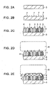
- FIGs. 2A to 2E are schematic diagrams showing a method for manufacturing the highly-oriented diamond film in order of processing according to this embodiment.
- FIGs. 2C to 2E non-oriented crystals are shown by fine hatching for easy view.
- a substrate 3 made of silicon, nickel, platinum, iridium, palladium, sapphire, gallium nitride, silicon carbide, strontium titanate, or the like is prepared.
- a bias voltage is applied to the substrate 3 under exposure to methane and hydrogen gas plasma in order to form oriented diamond nuclei 7 on a surface of the substrate 3.
- the ⁇ 111 ⁇ sector growth of diamond on the substrate 3 is performed by a chemical vapor deposition (CVD) method using a gaseous mixture of methane and hydrogen as material gas.
- CVD chemical vapor deposition
- ⁇ 1° is deposited.
- the diamond layer 1 having such a constitution crystal grain sizes in a diamond layer 2 to be deposited on the diamond layer 1 can be effectively increased.
- the thickness of the diamond layer 1 does not have any limitation as far as a sufficient degree of the orientation of the diamond crystals is achieved. However, the thinner diamond layer 1 is preferable for yielding the highly-oriented diamond film having a smaller thickness though an average crystal grain size being large.
- the surface state of the diamond layer 1 does not also have any limitation.
- the surface may be a flat face of predominant (100) planes parallel to the surface of the substrate 3 or may be a pyramidal state having a peak in the ⁇ 100> direction.
- the diamond layer 2 is deposited on the diamond layer 1 by the ⁇ 100 ⁇ sector growth of diamond by the CVD method using a gaseous mixture of methane, hydrogen, and oxygen as material gas.
- the CVD method when the surface has microscopic asperities, the growth rate at the salients is different from that at the reentrants.
- the most preferable example of the CVD method is a plasma CVD method in which electric field tends to converge to the salients, so the growth rate of diamond at the salients is higher than that at reentrants.
- a hot-filament CVD method in which electric field tends to converge to the salients by applying a bias voltage, so the growth rate of diamond at the salients is higher than that at the reentrants, can be also used.
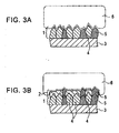
- FIGs. 3A and 3B are schematic diagrams showing film deposition states of the diamond layer 2 in order of processing when the gas pressure is lower than 133 hPa (which is outside of the scope of the present invention).
- active species hereinafter
- the active species reach the surface without substantial influence from microscopic asperities in the surface.
- plasma 6 equally covers the surface of the diamond layer 1 so as to trace the asperities formed in the surface of the diamond layer 1. Therefore, the difference in temperature is decreased and the growth rates become equal.
- FIG. 3B not only oriented crystals 4 but also non-oriented crystals 5 grow, so many non-oriented crystals 5 also appear in the surface of the diamond film and the flatness of the surface is decreased. Furthermore, the crystal size-increasing rate is also decreased.
- the free paths of the active species are short.
- electrode distribution between plasma and a diamond film has a property to focus on salients.
- the active species hardly reach the reentrants. Therefore, the growth rate at the reentrants is decreased because the plasma 6 becomes weak to decrease the temperature.
- the growth rate at the salients is increased because a large amount of active species reach the salients to increase the temperature.
- oxygen has an effect to etch defects generated in the diamond layer, and the effect is increased with the temperature. Therefore, as shown in FIG. 2E, when the material gas contains oxygen atoms at an adequate content as in this embodiment, the occurrence of the non-diamond carbon, the microcrystalline diamond, and the twin-crystalline diamond in the diamond layer can be suppressed. Consequently, the asperities in the surface of the diamond layer do not grow larger than a certain difference in the height; thus, the surface is planarized.
- the shape of the diamond layer 1 of the lower layer at this stage is important. Since the diamond layer 1 is synthesized under conditions such that the growth rate in the ⁇ 100> direction is the highest, each crystal has a pyramidal state having a peak in the ⁇ 100> direction. However, the ⁇ 100> direction of each crystal has a tilt against the substrate at within ⁇ 5°. It is believed that this is caused by difference in lattice constants of silicon and diamond. Since the growth rate at the ⁇ 100> direction is thought to be constant, a crystal having the highest peak against the surface of the substrate does not have a tilt. When the diamond layer 2 is deposited, a crystal having a higher peak grows faster. Therefore, crystals not having a tilt preferentially grow and increase the gain size. Then, only the crystals not having a tilt further grow to become into contact with each other at grain boundaries. This readily causes coalescence of a plurality of crystals, so the grain size is acceleratingly increased.
- the material gas composition and the substrate temperature during the deposition of the diamond layer 2 also have influence on the properties of the film. Therefore, in the method for manufacturing the highly-oriented diamond film according to this embodiment, the material gas composition is preferably determined such that a value calculated by dividing a difference between an amount (mole) of carbon atoms [C] and an amount (mole) of oxygen atoms [O] by an amount (mole) of total gas molecules [CH 3 + H 2 + O 2 ], i.e., ([C] - [O])/[CH 3 + H 2 + O 2 ], is -0.2 x 10 -2 or more and a ratio of the amount (mole) of oxygen atoms [O] to the amount (mole) of carbon atoms [C], i.e., [O]/[C], is 1.2 or less.
- the preferable range of ([C] - [O])/[CH 3 + H 2 + O 2 ] is from 0 to 0.04, and the preferable range of [O]/[C] is from 0 to 1.00.
- the substrate temperature is higher than 750°C and is lower than 1000°C.
- the upper limit of the substrate temperature is 900°C when a value calculated by dividing a difference between an amount (mole) of carbon atoms [C] and an amount (mole) of oxygen atoms [O] by an amount (mole) of total gas molecules [CH 3 + H 2 + O 2 ] is 1.0 ⁇ 10 -2 or more, or when a ratio ([O]/[C]) of an amount (mole) of oxygen atoms [O] to an amount (mole) of carbon atoms [C] is 0.5 or less.
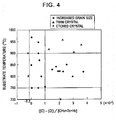
- FIG. 4 is a graph showing the relationship among material gas, substrate temperature, and film properties of the diamond layer 2 by plotting ([C] - [O]) / [CH 3 + H 2 + O 2 ] on the horizontal axis and substrate temperature on the vertical axis.
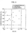
- FIG. 5 is a graph showing the relationship among material gas, substrate temperature, and film properties of the diamond layer 2 by plotting [O]/[C] on the horizontal axis and substrate temperature on the vertical axis. As shown in FIGs.
- twin crystals are generated in the diamond layer 2 to increase defects by raising the substrate temperatures to higher than 900°C.
- the diamond layer 1 is deposited by ⁇ 111 ⁇ sector growth and has substantially constant crystal grain size.
- the diamond layer 2 is deposited by ⁇ 100 ⁇ sector growth on the diamond layer 1 so that the crystal grain size of the diamond layer 2 increases with distance from the diamond layer 1.
- a highly-oriented diamond film including the diamond layer 1 and the diamond layer 2 deposited on the diamond layer 1 is yield.
- the diamond layer 1 and the diamond layer 2 are deposited by ⁇ 111 ⁇ sector growth and ⁇ 100 ⁇ sector growth, respectively; which can be confirmed by cathodoluminescence spectra.
- band A a luminescent band referred to as band A, which has a peak at 420 to 440 nm and a half-width of about 70 nm, weakly appears in the ⁇ 111 ⁇ sector growth and strongly appears in the ⁇ 100 ⁇ sector growth. Therefore, in the cathodoluminescence spectra of the highly-oriented diamond film according to this embodiment, band A is hardly observed and a 575 nm center is predominant in the diamond layer 1. On the other hand, band A appears stronger than the 575 nm center in the diamond layer 2. This proves that the diamond layer 1 has been deposited by the ⁇ 111 ⁇ sector growth and the diamond layer 2 has been deposited by the ⁇ 100 ⁇ sector growth.
- the second diamond layer 2 In the beginning of the ⁇ 100 ⁇ sector growth, oxygen at a low content is better from the viewpoint of the growth rate. When oxygen exists at a high content from the beginning, the growth rate is slow. However, when the growth rate is too high, the grain size cannot be sufficiently increased. Consequently, by controlling the oxygen gas content from the viewpoint of these respects, the second diamond layer can be also deposited by the ⁇ 100 ⁇ sector growth of diamond crystals. The second diamond layer can be efficiently deposited with a balance between the growth rate and the increase of grain size by using the oxygen gas at a low content (O/C) in the beginning and then increasing the oxygen gas content gradually or stepwise.
- O/C oxygen gas at a low content
- the surface of the highly-oriented diamond film according to this embodiment is flat and hardly contains non-oriented crystals, so a process, such as polishing, for planarizing the surface is unnecessary. Furthermore, the highly-oriented diamond film used in an electronic device does not prevent the conduction of electric charge. Furthermore, even if a diamond film is epitaxially deposited on the surface of the highly-oriented diamond film, variation in the impurity content does not occur and the planarity of the surface after the deposition is not lost. Thus, the highly-oriented diamond film has such advantageous effects.
- the highly-oriented diamond film according to this embodiment has a large average crystal grain size of 50 ⁇ m or more and the crystal grain size sharply increases such that the grain-size-increasing rate M is 50% or more, so a highly-oriented diamond film having large grain sizes though the film thickness being smaller than that of conventional films can be yielded. Consequently, the highly-oriented diamond films according to this embodiment are suitable for the use in electronic devices, such as transistors and diodes, in which the grain boundaries and non-oriented crystals may cause a decrease in performance, and are suitable as light-transmission windows. Improvement of performance and a decrease in manufacturing cost can be achieved by the application of the highly-oriented diamond film.
- a silicon substrate having a surface constituted by (100) planes was placed in a microwave CVD system and was irradiated with microwaves at a substrate temperature of 650°C for 15 mins under a flow of a gaseous mixture of 2% methane by volume and 98% hydrogen by volume under conditions with a pressure of 33 hPa and a flow rate of 300 standard cm 3 /min (sccm) .
- the microwave input power was about 1 kW and then was slightly controlled so as to maintain the substrate temperature at 650°C.
- a negative bias voltage was applied to the silicon substrate so that a current of 10 mA/cm 2 flows.
- oriented diamond nuclei were formed on the surface of the silicon substrate.
- a diamond layer was deposited on the silicon substrate so as to have a thickness of about 2 to 8 ⁇ m by ⁇ 111 ⁇ sector growth of diamond crystals with the microwave CVD system by using a gaseous mixture of 2% methane by volume and 98% hydrogen by volume as material gas at a substrate temperature of 800 to 850°C under a flow of the material gas under conditions with a pressure of 160 hPa and a flow rate of 400 standard cm 3 /min (sccm).
- the crystal grain sizes of this diamond layer were substantially constant.
- Diamond films of Examples 1 to 16 and Comparative Examples 1 to 9 were prepared by depositing diamond crystals by ⁇ 100 ⁇ sector growth on the diamond layer deposited by the ⁇ 111 ⁇ sector growth using a gaseous mixture of methane, hydrogen, and oxygen as material gas under conditions shown in Table 1.
- the pressure of the material gas was 160 hPa and the flow rate of the whole gas was 400 standard cm 3 /min (sccm). Film deposition rates, grain-size-increasing rates, and surface states of the resulting diamond films were evaluated. The results are shown in Table 1.
- diamond films of Comparative Examples 1 to 4 in which the substrate temperature was higher than 900°C had surfaces containing twin crystals, although [O] / [C] was 0.5 or less.
- the substrate temperature was 750°C or less
- diamond was etched during the ⁇ 100 ⁇ sector growth, so diamond layers were not deposited on the diamond layers prepared by the ⁇ 111 ⁇ sector growth.
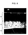
- FIG. 6 is a scanning electron microscope (SEM) photograph (x 350) of the highly-oriented diamond film according to this test. As shown in FIG. 6, the grain size r 11 of the first diamond layer 11 deposited on the silicon substrate 13 was about 3 ⁇ m on an average.
- the grain size r 12 was increased to 8 ⁇ m (grain-size-increasing rate: about 60%) and the surface became flat. Furthermore, the film was deposited until the film thickness became 25 ⁇ m under the same conditions, but the grain-size-increasing rate was decreased. Additionally, the grain size started to increase again by depositing a third diamond layer on the diamond layer 12 under modified conditions, and the average crystal grain size increased to 35 ⁇ m (grain-size-increasing rate: 68%) till the film thickness became about 40 ⁇ m. Then, the grain-size-increasing rate was decreased. Finally, the highly-oriented diamond film having an average crystal grain size of 35 ⁇ m and the surface being flat and hardly containing non-oriented crystals was yielded.
- FIG. 7A is a SEM photograph (x 250) of a cross-section of the diamond film of Example 8
- FIG. 7B is the cathodoluminescence image (x 250).
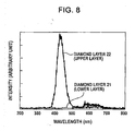
- FIG. 8 is a graph showing cathodoluminescence spectra of the diamond film of Example 8 by plotting wavelength on the horizontal axis and intensity on the vertical axis.
- the diamond film of Example 8 had a diamond layer 22 on a diamond layer 21.
- the grain sizes of the diamond layer 22 increased with growth and the grain sizes of the diamond layer 21 were substantially constant.
- the diamond layer 22 of the upper layer is seen to have two layers, but this is not changes in the properties of the film. This is caused by charge-up at observation time.
- the white portion was emitting light having a wavelength of 431 nm.
- the diamond layer 22 of the upper layer was evidently emitting light, but the diamond layer 21 of the lower layer was barely emitting light.
- the diamond layer 22 of the upper layer predominantly emitted a light having a wavelength of 431 nm and slightly emitted a light having a wavelength of 575 nm center.
- the diamond layer 21 of the lower layer barely emitted a light having a wavelength of 431 nm and emitted a light having a wavelength of 575 nm center alone. This also proves that the diamond layer 21 of the lower layer was mainly deposited by ⁇ 111 ⁇ sector growth and the diamond layer 22 of the upper layer was mainly deposited by ⁇ 100 ⁇ sector growth.
- the highly-oriented diamond films according to the present invention are suitable for the use in electronic devices such as transistors and diodes and are suitable as light-transmission windows.
- a highly-oriented diamond film which has a flat surface but does not have non-oriented crystals in the surface can be provided by depositing a first diamond layer on a substrate by ⁇ 111 ⁇ sector growth of diamond crystals by a CVD method using a gaseous mixture of methane and hydrogen as material gas, and then depositing a second diamond layer on the first diamond layer by ⁇ 100 ⁇ sector growth of diamond crystals by a plasma CVD method using a gaseous mixture of methane, hydrogen, and oxygen as material gas under the conditions that the pressure of the material gas is 133 hPa or more; the material gas composition is determined such that ([C] - [O])/[CH 3 + H 2 + O 2 ] is -0.2 x 10 -2 or more and [O]/[C] is 1.2 or less; and the substrate temperature is between 750°C and 1000°C.
Landscapes
- Chemical & Material Sciences (AREA)
- Engineering & Computer Science (AREA)
- Materials Engineering (AREA)
- Metallurgy (AREA)
- Organic Chemistry (AREA)
- Chemical Kinetics & Catalysis (AREA)
- General Chemical & Material Sciences (AREA)
- Mechanical Engineering (AREA)
- Crystallography & Structural Chemistry (AREA)
- Inorganic Chemistry (AREA)
- Physics & Mathematics (AREA)
- Combustion & Propulsion (AREA)
- Plasma & Fusion (AREA)
- Crystals, And After-Treatments Of Crystals (AREA)
- Chemical Vapour Deposition (AREA)
- Carbon And Carbon Compounds (AREA)
- Inorganic Insulating Materials (AREA)
Abstract
Description
- The present invention relates to highly-oriented diamond films of which crystal grains are highly oriented, methods for manufacturing the same, and electronic devices having highly-oriented diamond films. Specifically, the present invention relates to highly-oriented diamond films suitable for electronic devices such as transistors and diodes, methods for manufacturing the same, and electronic devices having the highly-oriented diamond films.
- A highly-oriented diamond film is a polycrystalline film in a broad sense, but a growth direction and an inplane direction of the crystal grains are each oriented in one direction and the surface is in a characteristic state of a series of flat (001) facets. Therefore, the highly-oriented diamond film is known that the crystal defect density near the surface is lower than that of general polycrystalline films and that the carrier mobility near the surface is about two figures higher than that of general polycrystalline films. Because of this, it is thought that the highly-oriented diamond film is suitable for electronic devices such as a field-effect transistor utilizing the carrier mobility in the lateral direction.
- Such a highly-oriented diamond film can be formed by, for example, subjecting a silicon substrate to microwave radiation while applying a negative bias voltage in a gas phase containing methane gas (US Patent No. 5,523,160). Furthermore, a method for preparing a heteroepitaxial diamond film having a flat surface is suggested in B. Dischler, C. Wild, eds. Low-Pressure Synthetic Diamond, 1998:153-158 (referred to as non-patent document, hereinafter). In the method, after the application of a bias voltage to a substrate, predominant [001] growth of diamond (a first growth) is performed at a rate of 3.9 to 4.5 µm/hr for improving a degree of orientation of crystal grains, and then surface-planarizing growth (a second growth) of diamond is performed at a rate of 2 µm/hr or less for planarizing the surface.
- The above-mentioned conventional technologies have some problems as follows: In an electronic device such as a transistor having a diamond film, properties of the device are improved with an increase in the diamond crystal grain size. For example, in the application to a transistor, since a gate length is generally 30 to 100 µm, the highly-oriented diamond film must have a crystal grain size of at least 30 µm, preferably 100 µm or more. When the highly-oriented diamond film is prepared according to the method disclosed in the non-patent document, diamond crystals grow in a columnar form in the first growth to gradually increase the grain sizes. However, since the increasing rate is small, a film having a large thickness is required for ensuring a crystal grain size of 30 µm or more; which is a problem.
- Furthermore, a diamond film having a flat surface is desirable. However, in the method described in the non-patent document, the diamond in the second growth is synthesized under such conditions that a growth rate in [111] orientation is higher than that in [001] orientation. Therefore, even if protruding non-oriented crystals are slight, the non-oriented crystals predominantly grow. When a highly-oriented diamond film containing non-oriented crystals is applied to an electronic device as a substrate, the surface is planarized by polishing after a film is epitaxially deposited on the diamond film for preventing inner damage caused by the polishing and for doping. This causes changes in growth sectors at the non-oriented crystal portions. Since distribution coefficients of an impurity differ in the growth sectors, the non-oriented crystal portions and the other portions each have an impurity content being different from that of each other when the epitaxially grown film is doped with the impurity. This is undesirable for device movement. Therefore, when the method disclosed in the non-patent document is conducted, the first growth must be performed until the non-oriented crystals do not protrude. Consequently, a thin film, for example, having a thickness of 50 µm or less cannot be formed by this method; which is a problem.
- The non-patent document discloses that a smooth diamond film having a film thickness is 5 µm or less can be formed by using a favorable SiC film as a buffer layer. However, in this case, a ratio of the average crystal grain size to the film thickness (average crystal grain size/film thickness) is still 1/2 or lower, so a large film thickness is required for yielding an average crystal grain size of 30 µm or more. This problem has not been solved yet.
- The present invention has been accomplished in view of such problems. Accordingly, it is an object of the present invention to provide a highly-oriented diamond film of which surface is flat and does not contain non-oriented crystals and of which crystal grain size is large though the film thickness being smaller than that of conventional films. Another object of the present invention is to provide a method for manufacturing the highly-oriented diamond film and an electronic device having the highly-oriented diamond film.
- A highly-oriented diamond film according to a first aspect of the present invention includes a first diamond layer deposited by {111} sector growth and a second diamond layer deposited on the first diamond layer by {100} sector growth so that the crystal grain sizes increase with distance from the first diamond layer, wherein
an average crystal grain size of the second diamond layer at the surface is represented by Da (µm); an average crystal grain size of the first diamond layer at the boundary of the first diamond layer and the second diamond layer or an average crystal grain size of the first diamond layer at a cross-section being the closest to the boundary and parallel to the surface of the second diamond layer when the boundary is not parallel to the surface of the second diamond layer is represented by Db (µm); and a distance from the surface of the second diamond layer to the boundary or the cross-section is represented by L (µm), wherein
a grain-size-increasing rate M (%) that is calculated by the following mathematical formula:
is 50% or higher. - In the present invention, since the crystal grain size sharply increases such that the grain-size-increasing rate M is 50% or more, a highly-oriented diamond film having large grain sizes though the film thickness being smaller than that of conventional films can be yielded. Additionally, since the highly-oriented diamond film has the second diamond layer deposited by the {100} sector growth on the first diamond layer deposited by the {111} sector growth, the surface is flat and hardly contains non-oriented crystals. With this, a process, such as polishing, for planarizing the surface is unnecessary. Furthermore, the highly-oriented diamond film used in an electronic device does not prevent the conduction of electric charge. Additionally, even if diamond is epitaxially deposited on the surface of the highly-oriented diamond film, variation in impurity content does not occur; thus, an epitaxial film of diamond having a flat surface can be yielded.
- The superficial layer at the second diamond layer side of the first diamond layer can be formed such that differences (Δα, Δβ, Δγ} between Euler angles {α, β, γ} of adjacent crystal grains are |Δα| ≤ 1°, |Δβ| ≤ 1°, and |Δγ| ≤ 1°. With this, the second diamond layer can be deposited on the first diamond layer so that the surface is flat and hardly contains non-oriented crystals. Here, Euler angles {α, β, γ} are values showing crystal orientation of a crystal grain.
- The average crystal grain size at the surface of the second diamond layer is preferably 30 µm or more, more preferably 100 µm or more. With this, characteristics of a transistor to which the highly-oriented diamond film is applied can be improved.
- The surface of the second diamond layer can be made of (100) planes. With this, the surface can be planarized.
- A method for manufacturing a highly-oriented diamond film according to a second aspect of the present invention includes:
- a step of depositing a first diamond layer on a substrate by {111} sector growth of diamond crystals by a chemical vapor deposition method; and
- a step of depositing a second diamond layer on the first diamond layer by {100} sector growth of diamond crystals by a chemical vapor deposition method using a material gaseous mixture containing carbon-containing gas and oxygen gas, wherein
- the gas pressure of the material gas is 133 hPa or more;
- the material gas composition is determined such that a value calculated by dividing a difference between an amount (mole) of carbon atoms and an amount (mole) of oxygen atoms by an amount (mole) of total gas molecules is -0.2 × 10⁻² or more and a ratio (O/C) of the amount (mole) of oxygen atoms to the amount (mole) of carbon atoms is 1.2 or less; and
- a substrate temperature is higher than 750°C and is lower than 1000°C.
- In the present invention, defects in the second diamond layer can be decreased and the average grain-size-increasing rate can be increased to 50% or more by optimizing conditions of gas-phase composition when the second diamond layer is deposited.
- In the method for manufacturing the highly-oriented diamond film, the substrate temperature in the step of depositing the second diamond layer may be between 750°C and 900°C when the material gas composition is such that a value calculated by dividing the difference between the amount (mole) of carbon atoms and the amount (mole) of oxygen atoms by the amount (mole) of total gas molecules is 1.0 x 10⁻² or more or such that a ratio (O/C) of the amount (mole) of oxygen atoms to the amount (mole) of carbon atoms is 0.5 or less. With this, occurrence of defects in the second diamond layer can be suppressed.
- The second diamond layer can be deposited, for example, by a plasma vapor deposition method or a hot-filament vapor deposition method. With this, non-oriented crystals in the surface of the second diamond layer can be decreased.
- In the step of depositing the first diamond layer, oriented diamond nuclei may be formed on a surface of the substrate. Then, the first diamond layer may be deposited on the substrate by {111} sector growth of diamond crystals by a chemical vapor deposition method using a material gaseous mixture not containing oxygen gas.
- In the step of depositing the second diamond layer, the second diamond layer may be deposited by {100} sector growth of diamond crystals while gradually or stepwise raising the ratio of oxygen gas. With this, the second diamond layer can be efficiently deposited with proper balance of an increase in the grain size and a growth rate.
- A diamond electronic device according to a third aspect of the present invention includes the above-mentioned highly-oriented diamond film.
- According to the present invention, since the diamond electronic device has the above-mentioned highly-oriented diamond film, the characteristics can be improved and the cost can be decreased in comparison with the conventional diamond electronic devices.
- The electronic device may be, for example, a transistor.
- According to the present invention, the crystal grain sizes are sharply increased so that the grain-size-increasing rate M is 50% or more. Therefore, the crystal grain sizes can be increased though the film thickness being smaller than that of conventional films. The second diamond layer is deposited by the {100} sector growth on the first diamond layer deposited by the {111} sector growth. Therefore, the highly-oriented diamond film of which surface is flat and does not contain non-oriented crystals can be yielded.
-
- FIG. 1 is a schematic cross-sectional view of a highly-oriented diamond film according to an embodiment of the present invention.
- FIGs. 2A to 2E are schematic diagrams showing a method for manufacturing a highly-oriented diamond film in order of processing according to an embodiment of the present invention.
- FIGs. 3A and 3B are schematic diagrams showing film states of a
diamond layer 2 in order of processing when the gas pressure is less than 130 hPa (which is outside of the scope of the present invention). - FIG. 4 is a graph showing the relationship among material gas, substrate temperature, and film properties of the
diamond layer 2 by plotting ([C] - [O])/[CH3 + H2 + O2] on the horizontal axis and substrate temperature on the vertical axis. - FIG. 5 is a graph showing the relationship among material gas, substrate temperature, and film properties of the
diamond layer 2 by plotting [O]/[C] on the horizontal axis and substrate temperature on the vertical axis. - FIG. 6 is a photograph (SEM photograph: x 350) of a highly-oriented diamond film of a second test according to the present invention.
- FIG. 7A is a photograph (SEM photograph: x 250) of a cross-section of a diamond film of Example 8 according to the present invention, and FIG. 7B is a photograph (x 250) of cathodoluminescence image of the diamond film.
- FIG. 8 is a graph showing cathodoluminescence spectra of the diamond film of Example 8 by plotting wavelength on the horizontal axis and intensity on the vertical axis.
- Highly-oriented diamond films according to the embodiments of the present invention will now be specifically described with reference to the attached drawings. FIG. 1 is a schematic diagram showing a highly-oriented diamond film according to an embodiment. In FIG. 1, non-oriented crystals are shown by fine hatching for easy view. As shown in FIG. 1, the highly-oriented diamond film according to this embodiment includes a
first diamond layer 1 having substantially constant crystal grain sizes and asecond diamond layer 2 on thefirst diamond layer 1. Thesecond diamond layer 2 includes a portion of which crystal grain sizes increase with distance from thefirst diamond layer 1. Diamond crystals which appear in the surface of the second diamond layer are formed by continuous growth of the crystals from the boundary between the first diamond layer and the second diamond layer at a grain-size-increasing rate of 50% or more. - The
diamond layer 1 is mainly deposited by {111} sector growth of diamond crystals on asubstrate 3 made of silicon, nickel, platinum, iridium, palladium, sapphire, gallium nitride, silicon carbide, strontium titanate, or the like. In this case, when differences {(α1 - α2), (β1 - β2), (γ1 - γ2)} between Euler angles {α1, β1, γ1} and {α2, β2, γ2} of the respective adjacent crystal grains are defined as {Δα, Δβ, Δγ}, a superficial layer at thediamond layer 2 side of thediamond layer 1 preferably has the differences such that |△α| ≤ 1°, |△β| ≤ 1°, and |△γ| ≤ 1°. With this, thediamond layer 2 which has a flat surface hardly containing non-oriented crystals can be deposited on thediamond layer 1. The superficial layer contains thediamond layer 1 in the range of at least 50 µm from the surface at thediamond layer 2 side of thediamond layer 1 in the thickness direction. - The
diamond layer 2 is mainly deposited by {100} sector growth of diamond crystals. The surface, namely, the surface of the highly-oriented diamond film according to this embodiment is a flat plane constituted by (100) planes. The surface of thesecond diamond layer 2 preferably has an average roughness Ra of 100 nm or less at the portions other than the grain boundaries. The average roughness Ra in this embodiment is based on JIS B0601: Arithmetic Average Roughness Ra. Thediamond layer 2 is mainly constituted by orientedcrystals 4, and the surface hardly containsnon-oriented crystals 5. The average crystal grain size at the surface of thediamond layer 2 is 30 µm or more. The grain size can be increased to about 10 mm, but a grain size of 100 µm to 1 mm is preferable. - In the highly-oriented diamond film according to this embodiment, the average crystal grain size of the
second diamond layer 2 at the surface is represented by Da (µm). When the boundary (shown by the A-A line in FIG. 1) of thefirst diamond layer 1 and thesecond diamond layer 2 is parallel to the surface of thesecond diamond layer 2, the average crystal grain size of thefirst diamond layer 1 at the boundary is represented by Db (µm). When the boundary is not parallel to the surface of thesecond diamond layer 2, the average grain size of thefirst diamond layer 1 at the cross-section which is parallel to the surface of thesecond diamond layer 2 and is the closest to the boundary in thefirst diamond layer 1 is represented by Db (µm). Furthermore, a distance between the surface of thediamond layer 2 and the boundary or the cross-section (A-A line) is represented by L (µm) . In the present invention, the grain-size-increasing rate M (%) calculated by the followingmathematical formula 2 using the Da, Db, and L is 50% or higher. A larger grain-size-increasing rate M is preferable. In the highly-oriented diamond film according to this embodiment, a grain-size-increasing rate M of about 500% can be achieved by adjusting manufacturing conditions. The grain-size-increasing rate M is preferably 60% to 500%, more preferably 60% to 200%, from the viewpoint of the balance with a film deposition rate.
- A method for manufacturing the highly-oriented diamond film according to this embodiment will now be described. FIGs. 2A to 2E are schematic diagrams showing a method for manufacturing the highly-oriented diamond film in order of processing according to this embodiment. In FIGs. 2C to 2E, non-oriented crystals are shown by fine hatching for easy view. Firstly, with reference to FIG. 2A, a
substrate 3 made of silicon, nickel, platinum, iridium, palladium, sapphire, gallium nitride, silicon carbide, strontium titanate, or the like is prepared. Then, with reference to FIG. 2B, a bias voltage is applied to thesubstrate 3 under exposure to methane and hydrogen gas plasma in order to form orienteddiamond nuclei 7 on a surface of thesubstrate 3. - With reference to FIG. 2C, the {111} sector growth of diamond on the
substrate 3 is performed by a chemical vapor deposition (CVD) method using a gaseous mixture of methane and hydrogen as material gas. This suppresses the growth of non-oriented crystals and generates differences in height ofnon-oriented crystals 5 and orientedcrystals 4; thus, adiamond layer 1 having a superficial layer in which differences {Δα, Δβ, Δy} between Euler angles of adjacent crystal grains are |Δα| ≤ 1°, |Δβ| ≤ 1°, and |Δγ| ≤ 1° is deposited. With thediamond layer 1 having such a constitution, crystal grain sizes in adiamond layer 2 to be deposited on thediamond layer 1 can be effectively increased. - The thickness of the
diamond layer 1 does not have any limitation as far as a sufficient degree of the orientation of the diamond crystals is achieved. However, thethinner diamond layer 1 is preferable for yielding the highly-oriented diamond film having a smaller thickness though an average crystal grain size being large. The surface state of thediamond layer 1 does not also have any limitation. For example, the surface may be a flat face of predominant (100) planes parallel to the surface of thesubstrate 3 or may be a pyramidal state having a peak in the <100> direction. - As shown in FIGs. 2D and 2E, the
diamond layer 2 is deposited on thediamond layer 1 by the {100} sector growth of diamond by the CVD method using a gaseous mixture of methane, hydrogen, and oxygen as material gas. In the CVD method, when the surface has microscopic asperities, the growth rate at the salients is different from that at the reentrants. The most preferable example of the CVD method is a plasma CVD method in which electric field tends to converge to the salients, so the growth rate of diamond at the salients is higher than that at reentrants. A hot-filament CVD method, in which electric field tends to converge to the salients by applying a bias voltage, so the growth rate of diamond at the salients is higher than that at the reentrants, can be also used. - At this stage, the pressure of the material gas is maintained at 133 hPa or higher. The crystal grain size of the
diamond layer 2 to be deposited increases with the gas pressure when thediamond layer 2 is deposited. The pressure of the material gas may be at around atmospheric pressure of 1013 hPa, but a material gas pressure of 267 hPa or less is preferable. FIGs. 3A and 3B are schematic diagrams showing film deposition states of thediamond layer 2 in order of processing when the gas pressure is lower than 133 hPa (which is outside of the scope of the present invention). When the gas pressure is lower than 133 hPa, free paths of active molecules and active atoms (these are collectively referred to as active species, hereinafter) in the material gas are long. Consequently, the active species reach the surface without substantial influence from microscopic asperities in the surface. As shown in FIG. 3A,plasma 6 equally covers the surface of thediamond layer 1 so as to trace the asperities formed in the surface of thediamond layer 1. Therefore, the difference in temperature is decreased and the growth rates become equal. As a result, as shown in FIG. 3B, not only orientedcrystals 4 but alsonon-oriented crystals 5 grow, so manynon-oriented crystals 5 also appear in the surface of the diamond film and the flatness of the surface is decreased. Furthermore, the crystal size-increasing rate is also decreased. - On the other hand, when the gas pressure is equal to or higher than 133 hPa as in this embodiment, the free paths of the active species are short. Generally, electrode distribution between plasma and a diamond film has a property to focus on salients. In a method for manufacturing the highly-oriented diamond film according to this embodiment, since the free paths of active species are short, as shown in FIG. 2D, the active species hardly reach the reentrants. Therefore, the growth rate at the reentrants is decreased because the
plasma 6 becomes weak to decrease the temperature. On the other hand, the growth rate at the salients is increased because a large amount of active species reach the salients to increase the temperature. As a result, crystals do not grow at the reentrants, i.e., on thenon-oriented crystals 5, but crystals grow larger at the salients, i.e., on the orientedcrystals 4. However, with this alone, the difference in height of the crystals is enhanced and the planarization of the surface cannot be achieved. Then, the increase of difference in the height of the crystals at the surface can be suppressed by adjusting the oxygen content in the material gas. When a salient height becomes large, the temperature at the salient increases too high, for example, it exceeds 1000°C. By using the material gas not containing oxygen atoms, non-diamond carbon, microcrystalline diamond, and twin-crystalline diamond start to grow at this salient. On the other hand, oxygen has an effect to etch defects generated in the diamond layer, and the effect is increased with the temperature. Therefore, as shown in FIG. 2E, when the material gas contains oxygen atoms at an adequate content as in this embodiment, the occurrence of the non-diamond carbon, the microcrystalline diamond, and the twin-crystalline diamond in the diamond layer can be suppressed. Consequently, the asperities in the surface of the diamond layer do not grow larger than a certain difference in the height; thus, the surface is planarized. - The shape of the
diamond layer 1 of the lower layer at this stage is important. Since thediamond layer 1 is synthesized under conditions such that the growth rate in the <100> direction is the highest, each crystal has a pyramidal state having a peak in the <100> direction. However, the <100> direction of each crystal has a tilt against the substrate at within ±5°. It is believed that this is caused by difference in lattice constants of silicon and diamond. Since the growth rate at the <100> direction is thought to be constant, a crystal having the highest peak against the surface of the substrate does not have a tilt. When thediamond layer 2 is deposited, a crystal having a higher peak grows faster. Therefore, crystals not having a tilt preferentially grow and increase the gain size. Then, only the crystals not having a tilt further grow to become into contact with each other at grain boundaries. This readily causes coalescence of a plurality of crystals, so the grain size is acceleratingly increased. - Furthermore, the material gas composition and the substrate temperature during the deposition of the
diamond layer 2 also have influence on the properties of the film. Therefore, in the method for manufacturing the highly-oriented diamond film according to this embodiment, the material gas composition is preferably determined such that a value calculated by dividing a difference between an amount (mole) of carbon atoms [C] and an amount (mole) of oxygen atoms [O] by an amount (mole) of total gas molecules [CH3 + H2 + O2], i.e., ([C] - [O])/[CH3 + H2 + O2], is -0.2 x 10⁻² or more and a ratio of the amount (mole) of oxygen atoms [O] to the amount (mole) of carbon atoms [C], i.e., [O]/[C], is 1.2 or less. Specifically, the preferable range of ([C] - [O])/[CH3 + H2 + O2] is from 0 to 0.04, and the preferable range of [O]/[C] is from 0 to 1.00. The substrate temperature is higher than 750°C and is lower than 1000°C. However, the upper limit of the substrate temperature is 900°C when a value calculated by dividing a difference between an amount (mole) of carbon atoms [C] and an amount (mole) of oxygen atoms [O] by an amount (mole) of total gas molecules [CH3 + H2 + O2] is 1.0 × 10⁻² or more, or when a ratio ([O]/[C]) of an amount (mole) of oxygen atoms [O] to an amount (mole) of carbon atoms [C] is 0.5 or less. - FIG. 4 is a graph showing the relationship among material gas, substrate temperature, and film properties of the
diamond layer 2 by plotting ([C] - [O]) / [CH3 + H2 + O2] on the horizontal axis and substrate temperature on the vertical axis. FIG. 5 is a graph showing the relationship among material gas, substrate temperature, and film properties of thediamond layer 2 by plotting [O]/[C] on the horizontal axis and substrate temperature on the vertical axis. As shown in FIGs. 4 and 5, when ([C] - [O]) / [CH3 + H2 + O2] is lower than -0.2 x 10⁻² or when [O] / [C] is higher than 1.2, diamond is etched during the {100} sector growth and thediamond layer 2 cannot be deposited. When the substrate temperature is 750°C or less, the film deposition rate becomes lower than 0.4 µm/hr. Therefore, the manufacturing cost increases and, concurrently, diamond is etched during the {100} sector growth and thediamond layer 2 cannot be deposited. Reversely, when substrate temperature is 1000°C or higher, twin crystals or microcrystals are generated in thediamond layer 2 to increase defects; which is impractical. When ([C]-[O]) / [CH3 + H2 + O2] is 1.0 x 10⁻² or more or when [O] / [C] is 0.5 or less, twin crystals are generated in thediamond layer 2 to increase defects by raising the substrate temperatures to higher than 900°C. - With reference to FIG. 1, the
diamond layer 1 is deposited by {111} sector growth and has substantially constant crystal grain size. Thediamond layer 2 is deposited by {100} sector growth on thediamond layer 1 so that the crystal grain size of thediamond layer 2 increases with distance from thediamond layer 1. Thus, a highly-oriented diamond film including thediamond layer 1 and thediamond layer 2 deposited on thediamond layer 1 is yield. Thediamond layer 1 and thediamond layer 2 are deposited by {111} sector growth and {100} sector growth, respectively; which can be confirmed by cathodoluminescence spectra. Specifically, in a cathodoluminescence spectrum, a luminescent band referred to as band A, which has a peak at 420 to 440 nm and a half-width of about 70 nm, weakly appears in the {111} sector growth and strongly appears in the {100} sector growth. Therefore, in the cathodoluminescence spectra of the highly-oriented diamond film according to this embodiment, band A is hardly observed and a 575 nm center is predominant in thediamond layer 1. On the other hand, band A appears stronger than the 575 nm center in thediamond layer 2. This proves that thediamond layer 1 has been deposited by the {111} sector growth and thediamond layer 2 has been deposited by the {100} sector growth. - The deposition of the
second diamond layer 2 will now be described. In the beginning of the {100} sector growth, oxygen at a low content is better from the viewpoint of the growth rate. When oxygen exists at a high content from the beginning, the growth rate is slow. However, when the growth rate is too high, the grain size cannot be sufficiently increased. Consequently, by controlling the oxygen gas content from the viewpoint of these respects, the second diamond layer can be also deposited by the {100} sector growth of diamond crystals. The second diamond layer can be efficiently deposited with a balance between the growth rate and the increase of grain size by using the oxygen gas at a low content (O/C) in the beginning and then increasing the oxygen gas content gradually or stepwise. - The surface of the highly-oriented diamond film according to this embodiment is flat and hardly contains non-oriented crystals, so a process, such as polishing, for planarizing the surface is unnecessary. Furthermore, the highly-oriented diamond film used in an electronic device does not prevent the conduction of electric charge. Furthermore, even if a diamond film is epitaxially deposited on the surface of the highly-oriented diamond film, variation in the impurity content does not occur and the planarity of the surface after the deposition is not lost. Thus, the highly-oriented diamond film has such advantageous effects. Additionally, the highly-oriented diamond film according to this embodiment has a large average crystal grain size of 50 µm or more and the crystal grain size sharply increases such that the grain-size-increasing rate M is 50% or more, so a highly-oriented diamond film having large grain sizes though the film thickness being smaller than that of conventional films can be yielded. Consequently, the highly-oriented diamond films according to this embodiment are suitable for the use in electronic devices, such as transistors and diodes, in which the grain boundaries and non-oriented crystals may cause a decrease in performance, and are suitable as light-transmission windows. Improvement of performance and a decrease in manufacturing cost can be achieved by the application of the highly-oriented diamond film.
- The advantageous effects of the present invention will now be described with reference to Examples in comparison with Comparative Examples which are out of the scope of the present invention.
- Firstly, the results of a first test will be described. A silicon substrate having a surface constituted by (100) planes was placed in a microwave CVD system and was irradiated with microwaves at a substrate temperature of 650°C for 15 mins under a flow of a gaseous mixture of 2% methane by volume and 98% hydrogen by volume under conditions with a pressure of 33 hPa and a flow rate of 300 standard cm3/min (sccm) . At this time, the microwave input power was about 1 kW and then was slightly controlled so as to maintain the substrate temperature at 650°C. Simultaneously, a negative bias voltage was applied to the silicon substrate so that a current of 10 mA/cm2 flows. Thus, oriented diamond nuclei were formed on the surface of the silicon substrate.
- Then, a diamond layer was deposited on the silicon substrate so as to have a thickness of about 2 to 8 µm by {111} sector growth of diamond crystals with the microwave CVD system by using a gaseous mixture of 2% methane by volume and 98% hydrogen by volume as material gas at a substrate temperature of 800 to 850°C under a flow of the material gas under conditions with a pressure of 160 hPa and a flow rate of 400 standard cm3/min (sccm). The crystal grain sizes of this diamond layer were substantially constant.
- Diamond films of Examples 1 to 16 and Comparative Examples 1 to 9 were prepared by depositing diamond crystals by {100} sector growth on the diamond layer deposited by the {111} sector growth using a gaseous mixture of methane, hydrogen, and oxygen as material gas under conditions shown in Table 1. At this time, the pressure of the material gas was 160 hPa and the flow rate of the whole gas was 400 standard cm3/min (sccm). Film deposition rates, grain-size-increasing rates, and surface states of the resulting diamond films were evaluated. The results are shown in Table 1.
Table 1 Film-forming condition Evaluation result CH3 flow rate (sccm) O2 flow rate (sccm) [O]/[C] ([C]-[O])/ [CH3+O2+H2] Substrate temperature (°C) Film-forming rate (µm/hr) Increasing rate of grain size (%) Surface state Example 1 5.0 0.50 0.20 1.00×10⁻² 754 0.4 72 Increased grain size Example 2 5.0 1.50 0.60 0.50×10⁻² 950 1.7 112 Increased grain size Example 3 5.0 2.50 1.00 0.00 969 0.6 93 Increased grain size Example 4 10.0 1.50 0.30 1.74×10⁻² 840 0.7 65 Increased grain size Example 5 15.0 2.50 0.33 2.48×10⁻² 851 1.0 76 Increased grain size Example 8 10.0 0.50 0.10 2.25×10⁻² 821 15.0 59 Increased grain size Example 7 10.0 1.00 0.20 2.00×10⁻² 821 12.3 72 Increased grain size Example 8 10.0 1.20 0.24 1.89×10⁻² 821 9.1 79 Increased grain size Example 9 10.0 2.00 0.40 1.49×10⁻² 830 7.8 86 Increased grain size Example 10 10.0 4.00 0.80 0.50×10⁻² 900 1.0 98 Increased grain size Example 11 35.0 10.00 0.57 3.66×10⁻² 820 17.3 74 Increased grain size Example 12 6.0 1.80 0.60 0.60×10⁻² 870 1.1 59 Increased grain size Example 13 15.0 7.50 1.00 0.00 850 0.7 68 Increased grain size Example 14 7.5 2.25 0.60 0.75×10⁻² 800 2.1 85 Increased grain size Example 15 40.0 14,00 0.70 2.90×10⁻² 800 6.5 70 Increased grain size Comparative Example 1 10.0 0.50 0.10 2.25×10⁻² 958 5.6 43 Having twin-crystal Comparative Comparative Example 2 10.0 2.50 0.50 1.24×10⁻² 920 5.1 22 Having twin-crystal Comparative Example 3 15.0 0.50 0.07 3.50×10⁻² 940 11.1 19 Having twin-crystal Comparative Example 4 15.0 1.50 0.20 2.89×10⁻² 906 6.8 22 Having twin-crystal Comparative Example 5 5.0 1.50 0.60 0.50×10⁻² 750 - - Etched crystal Comparative Example 6 5.0 2.50 1.00 0.00 750 - - Etched crystal Comparative Example 7 5.0 3.00 1.20 -0.25×10⁻² 600 - - Etched crystal Comparative Example 8 5.0 3.00 1.20 -0.25×10⁻² 900 - - Etched crystal Comparative Example 9 10.0 1.00 0.20 2.00×10⁻² 700 - - Etched crystal - As shown in Table 1, diamond films of Comparative Examples 1 to 4 in which the substrate temperature was higher than 900°C had surfaces containing twin crystals, although [O] / [C] was 0.5 or less. In the diamond films of Comparative Examples 5, 6, and 9 in which the substrate temperature was 750°C or less, diamond was etched during the {100} sector growth, so diamond layers were not deposited on the diamond layers prepared by the {111} sector growth. Additionally, in the diamond films of Comparative Examples 7 and 8 in which ([C] - [O]) / [CH3 + H2 + O2] was lower than 0.2 x 10⁻², diamond was similarly etched during the {100} sector growth, so diamond layers were not deposited on the diamond layers prepared by the {111} sector growth. On the other hand, all diamond films of Examples 1 to 15 exhibited a grain-size-increasing rate of higher than 50%, and the average rate was 70% and the highest rate was 112% (Example 2). Non-orientation was not observed in the surfaces of these diamond films, and the surfaces were flat. Furthermore, even the lowest film deposition rate was 0.4 µm/hr (Example 1) and the highest film deposition rate was 17.3 µm/hr (Example 11) .
- As Comparative Example 10, diamond layers were deposited by {100} sector growth of diamond crystals on each of the diamond layers deposited by the {111} sector growth of diamond crystals under the same conditions as in Examples 6, 7, and 8 except that the material gas pressure was 67 hPa. The surfaces of all diamond films were flat, but the crystal grain sizes were not substantially increased and some non-oriented crystals were observed in the surfaces. Furthermore, the film deposition rate was 0.3 µm/hr or less.
- Next, the results of a second test will be described. With the same method and conditions as in the first test, diamond crystals were deposited on a silicon substrate by {111} sector growth, and then diamond crystals were deposited by {100} sector growth on the resulting diamond layer under the same conditions as in Example 6 shown in Table 1. Then, diamond crystals were further deposited by {100} sector growth under the same conditions as in Example 7 shown in Table 1. Changes in the grain sizes were observed. FIG. 6 is a scanning electron microscope (SEM) photograph (x 350) of the highly-oriented diamond film according to this test. As shown in FIG. 6, the grain size r11 of the
first diamond layer 11 deposited on thesilicon substrate 13 was about 3 µm on an average. When the film thickness of thesecond diamond layer 12 was 8 µm, the grain size r12 was increased to 8 µm (grain-size-increasing rate: about 60%) and the surface became flat. Furthermore, the film was deposited until the film thickness became 25 µm under the same conditions, but the grain-size-increasing rate was decreased. Additionally, the grain size started to increase again by depositing a third diamond layer on thediamond layer 12 under modified conditions, and the average crystal grain size increased to 35 µm (grain-size-increasing rate: 68%) till the film thickness became about 40 µm. Then, the grain-size-increasing rate was decreased. Finally, the highly-oriented diamond film having an average crystal grain size of 35 µm and the surface being flat and hardly containing non-oriented crystals was yielded. - Next, the results of a third test will be described. The cross-section observation and cathodoluminescence measurement of the diamond film of Example 8 shown in Table 1 were performed. FIG. 7A is a SEM photograph (x 250) of a cross-section of the diamond film of Example 8, and FIG. 7B is the cathodoluminescence image (x 250). FIG. 8 is a graph showing cathodoluminescence spectra of the diamond film of Example 8 by plotting wavelength on the horizontal axis and intensity on the vertical axis. As shown in FIG. 7A, the diamond film of Example 8 had a
diamond layer 22 on adiamond layer 21. The grain sizes of thediamond layer 22 increased with growth and the grain sizes of thediamond layer 21 were substantially constant. In addition, in FIG. 7A, thediamond layer 22 of the upper layer is seen to have two layers, but this is not changes in the properties of the film. This is caused by charge-up at observation time. - In the cathodoluminescence image shown in FIG. 7B, the white portion was emitting light having a wavelength of 431 nm. As shown in FIG. 7B, the
diamond layer 22 of the upper layer was evidently emitting light, but thediamond layer 21 of the lower layer was barely emitting light. Furthermore, as shown in FIG. 8, thediamond layer 22 of the upper layer predominantly emitted a light having a wavelength of 431 nm and slightly emitted a light having a wavelength of 575 nm center. On the other hand, thediamond layer 21 of the lower layer barely emitted a light having a wavelength of 431 nm and emitted a light having a wavelength of 575 nm center alone. This also proves that thediamond layer 21 of the lower layer was mainly deposited by {111} sector growth and thediamond layer 22 of the upper layer was mainly deposited by {100} sector growth. - Thus, the highly-oriented diamond films according to the present invention are suitable for the use in electronic devices such as transistors and diodes and are suitable as light-transmission windows.
- A highly-oriented diamond film which has a flat surface but does not have non-oriented crystals in the surface can be provided by depositing a first diamond layer on a substrate by {111} sector growth of diamond crystals by a CVD method using a gaseous mixture of methane and hydrogen as material gas, and then depositing a second diamond layer on the first diamond layer by {100} sector growth of diamond crystals by a plasma CVD method using a gaseous mixture of methane, hydrogen, and oxygen as material gas under the conditions that the pressure of the material gas is 133 hPa or more; the material gas composition is determined such that ([C] - [O])/[CH3 + H2 + O2] is -0.2 x 10⁻² or more and [O]/[C] is 1.2 or less; and the substrate temperature is between 750°C and 1000°C.
Claims (12)
- A highly-oriented diamond film comprising a first diamond layer deposited by {111} sector growth and a second diamond layer deposited on the first diamond layer by {100} sector growth so that the crystal grain sizes increase with distance from the first diamond layer, wherein
an average crystal grain size of the second diamond layer at the surface is represented by Da (µm) ; an average crystal grain size of the first diamond layer at the boundary of the first diamond layer and the second diamond layer or an average crystal grain size of the first diamond layer at a cross-section of the first diamond layer being the closest to the boundary and parallel to the surface of the second diamond layer when the boundary is not parallel to the surface of the second diamond layer is represented by Db (µm); and a distance from the surface of the second diamond layer to the boundary or the cross-section is represented by L (µm), wherein
a grain size-increasing rate M (%) that is calculated by the following formula:
is 50% or higher. - The highly-oriented diamond film according to claim 1, wherein differences {Δα, Δβ, Δγ} between Euler angles {α, β, γ} of adjacent crystal grains in a superficial layer at the second diamond layer side of the first diamond layer are |△α| ≤ 1°, |△β| ≤ 1°, and |△γ| ≤ 1°.
- The highly-oriented diamond film according to claim 1 or 2, wherein the average crystal grain size at the surface of the second diamond layer is 30 µm or more.
- The highly-oriented diamond film according to claim 3, wherein the average crystal grain size at the surface of the second diamond layer is 100 µm or more.
- The highly-oriented diamond film according to any one of claims 1 to 4, wherein the surface of the second diamond layer is a (100) plane.
- A method for manufacturing a highly-oriented diamond film, the method comprising:a step of depositing a first diamond layer on a substrate by {111} sector growth of diamond crystals by a chemical vapor deposition method; anda step of depositing a second diamond layer on the first diamond layer by {100} sector growth of diamond crystals by a chemical vapor deposition method using a material gaseous mixture containing carbon-containing gas and oxygen gas, whereinthe gas pressure of the material gas is 133 hPa or more;the material gas composition is determined such that a value calculated by dividing a difference between an amount (mole) of carbon atoms and an amount (mole) of oxygen atoms by an amount (mole) of total gas molecules is -0.2 × 10⁻² or more and a ratio (O/C) of the amount (mole) of oxygen atoms to the amount (mole) of carbon atoms is 1.2 or less; anda substrate temperature is higher than 750°C and is lower than 1000°C.
- The method for manufacturing a highly-oriented diamond film according to claim 6, wherein the substrate temperature in the step of depositing the second diamond layer is higher than 750°C but does not exceed 900°C when the material gas composition is such that a value calculated by dividing the difference between the amount (mole) of carbon atoms and the amount (mole) of oxygen atoms by the amount (mole) of total gas molecules is 1.0 x 10⁻² or more or such that a ratio (O/C) of the amount (mole) of oxygen atoms to the amount (mole) of carbon atoms is 0.5 or less.
- The method for manufacturing a highly-oriented diamond film according to claim 6 or 7, wherein the second diamond layer is deposited by a plasma vapor deposition method or a hot-filament vapor deposition method.
- The method for manufacturing a highly-oriented diamond film according to any one of claims 6 to 8, wherein the step of depositing the first diamond layer is performed by formation of oriented diamond nuclei on the surface of the substrate and then by {111} sector growth of diamond crystals on the substrate by the chemical vapor deposition method using a material gaseous mixture not containing oxygen gas.
- The method for manufacturing a highly-oriented diamond film according to any one of claims 6 to 9, wherein the second diamond layer is deposited by {100} sector growth of diamond crystals while gradually or stepwise raising the ratio of oxygen gas in the step of depositing the second diamond layer.
- An electronic device having the highly-oriented diamond film according to any one of claims 1 to 5.
- The electronic device according to claim 11, wherein the electronic device is a transistor.
Applications Claiming Priority (2)
| Application Number | Priority Date | Filing Date | Title |
|---|---|---|---|
| JP2004344860 | 2004-11-29 | ||
| JP2005261335A JP4646752B2 (en) | 2004-11-29 | 2005-09-08 | Highly oriented diamond film, manufacturing method thereof, and electronic device provided with highly oriented diamond film |
Publications (3)
| Publication Number | Publication Date |
|---|---|
| EP1662021A2 true EP1662021A2 (en) | 2006-05-31 |
| EP1662021A3 EP1662021A3 (en) | 2006-06-07 |
| EP1662021B1 EP1662021B1 (en) | 2010-07-21 |
Family
ID=35871118
Family Applications (1)
| Application Number | Title | Priority Date | Filing Date |
|---|---|---|---|
| EP05024544A Expired - Lifetime EP1662021B1 (en) | 2004-11-29 | 2005-11-10 | Highly-oriented diamond film, method for manufacturing the same, and electronic device having highly-oriented diamond film |
Country Status (8)
| Country | Link |
|---|---|
| US (1) | US7311977B2 (en) |
| EP (1) | EP1662021B1 (en) |
| JP (1) | JP4646752B2 (en) |
| KR (1) | KR100736281B1 (en) |
| CN (1) | CN1804116B (en) |
| AT (1) | ATE474941T1 (en) |
| DE (1) | DE602005022397D1 (en) |
| TW (1) | TWI303670B (en) |
Cited By (1)
| Publication number | Priority date | Publication date | Assignee | Title |
|---|---|---|---|---|
| US11896964B2 (en) | 2018-12-06 | 2024-02-13 | Element Six (Uk) Limited | Polycrystalline diamond construction and method of making same |
Families Citing this family (259)
| Publication number | Priority date | Publication date | Assignee | Title |
|---|---|---|---|---|
| JP4953356B2 (en) * | 2006-09-25 | 2012-06-13 | 株式会社神戸製鋼所 | Porous diamond film and method for producing the same |
| JP5020147B2 (en) * | 2008-03-31 | 2012-09-05 | 株式会社神戸製鋼所 | Highly oriented diamond film and method for producing the same |
| FR2940326B1 (en) * | 2008-12-19 | 2011-03-25 | Centre Nat Rech Scient | METHOD FOR MANUFACTURING DIAMOND COMPOSITE MATERIALS |
| JP5377212B2 (en) | 2009-10-13 | 2013-12-25 | 信越化学工業株式会社 | Method for producing single crystal diamond substrate |
| JP5468528B2 (en) | 2010-06-28 | 2014-04-09 | 信越化学工業株式会社 | SUBSTRATE FOR GROWING SINGLE CRYSTAL DIAMOND, METHOD FOR PRODUCING THE SAME, AND METHOD FOR PRODUCING SINGLE CRYSTAL DIAMOND SUBSTRATE |
| JP2012031000A (en) * | 2010-07-29 | 2012-02-16 | Kobe Steel Ltd | Grain-arranged diamond film, and method for production thereof |
| US20130023129A1 (en) | 2011-07-20 | 2013-01-24 | Asm America, Inc. | Pressure transmitter for a semiconductor processing environment |
| US20160376700A1 (en) | 2013-02-01 | 2016-12-29 | Asm Ip Holding B.V. | System for treatment of deposition reactor |
| JP6335729B2 (en) * | 2013-12-06 | 2018-05-30 | キヤノン株式会社 | Transmission target and X-ray generating tube provided with the transmission target |
| US10858737B2 (en) | 2014-07-28 | 2020-12-08 | Asm Ip Holding B.V. | Showerhead assembly and components thereof |
| US10941490B2 (en) | 2014-10-07 | 2021-03-09 | Asm Ip Holding B.V. | Multiple temperature range susceptor, assembly, reactor and system including the susceptor, and methods of using the same |
| US10276355B2 (en) | 2015-03-12 | 2019-04-30 | Asm Ip Holding B.V. | Multi-zone reactor, system including the reactor, and method of using the same |
| US10907264B2 (en) * | 2015-06-10 | 2021-02-02 | Advanced Diamond Technologies, Inc. | Extreme durability composite diamond electrodes |
| US11139308B2 (en) | 2015-12-29 | 2021-10-05 | Asm Ip Holding B.V. | Atomic layer deposition of III-V compounds to form V-NAND devices |
| US10529554B2 (en) | 2016-02-19 | 2020-01-07 | Asm Ip Holding B.V. | Method for forming silicon nitride film selectively on sidewalls or flat surfaces of trenches |
| US10343920B2 (en) | 2016-03-18 | 2019-07-09 | Asm Ip Holding B.V. | Aligned carbon nanotubes |
| US11453943B2 (en) | 2016-05-25 | 2022-09-27 | Asm Ip Holding B.V. | Method for forming carbon-containing silicon/metal oxide or nitride film by ALD using silicon precursor and hydrocarbon precursor |
| US9859151B1 (en) | 2016-07-08 | 2018-01-02 | Asm Ip Holding B.V. | Selective film deposition method to form air gaps |
| US10612137B2 (en) | 2016-07-08 | 2020-04-07 | Asm Ip Holdings B.V. | Organic reactants for atomic layer deposition |
| US9887082B1 (en) | 2016-07-28 | 2018-02-06 | Asm Ip Holding B.V. | Method and apparatus for filling a gap |
| US9812320B1 (en) | 2016-07-28 | 2017-11-07 | Asm Ip Holding B.V. | Method and apparatus for filling a gap |
| CN106637143A (en) * | 2016-09-23 | 2017-05-10 | 常州大学 | Preparation method of MPCVD diamond film |
| EP3529397A4 (en) | 2016-10-20 | 2020-06-24 | Advanced Diamond Technologies, Inc. | OZONE GENERATORS, METHODS OF MANUFACTURING OZONE GENERATORS, AND METHODS OF OZONE GENERATION |
| US11532757B2 (en) | 2016-10-27 | 2022-12-20 | Asm Ip Holding B.V. | Deposition of charge trapping layers |
| US10714350B2 (en) | 2016-11-01 | 2020-07-14 | ASM IP Holdings, B.V. | Methods for forming a transition metal niobium nitride film on a substrate by atomic layer deposition and related semiconductor device structures |
| KR102546317B1 (en) | 2016-11-15 | 2023-06-21 | 에이에스엠 아이피 홀딩 비.브이. | Gas supply unit and substrate processing apparatus including the same |
| US11447861B2 (en) | 2016-12-15 | 2022-09-20 | Asm Ip Holding B.V. | Sequential infiltration synthesis apparatus and a method of forming a patterned structure |
| US11581186B2 (en) | 2016-12-15 | 2023-02-14 | Asm Ip Holding B.V. | Sequential infiltration synthesis apparatus |
| US11390950B2 (en) | 2017-01-10 | 2022-07-19 | Asm Ip Holding B.V. | Reactor system and method to reduce residue buildup during a film deposition process |
| US10468261B2 (en) | 2017-02-15 | 2019-11-05 | Asm Ip Holding B.V. | Methods for forming a metallic film on a substrate by cyclical deposition and related semiconductor device structures |
| US10770286B2 (en) | 2017-05-08 | 2020-09-08 | Asm Ip Holdings B.V. | Methods for selectively forming a silicon nitride film on a substrate and related semiconductor device structures |
| CN107267954B (en) * | 2017-06-14 | 2020-02-14 | 哈尔滨工业大学深圳研究生院 | Method for preparing highly-oriented diamond nanosheet array material through epitaxial growth |
| US12040200B2 (en) | 2017-06-20 | 2024-07-16 | Asm Ip Holding B.V. | Semiconductor processing apparatus and methods for calibrating a semiconductor processing apparatus |
| US11306395B2 (en) | 2017-06-28 | 2022-04-19 | Asm Ip Holding B.V. | Methods for depositing a transition metal nitride film on a substrate by atomic layer deposition and related deposition apparatus |
| KR20190009245A (en) | 2017-07-18 | 2019-01-28 | 에이에스엠 아이피 홀딩 비.브이. | Methods for forming a semiconductor device structure and related semiconductor device structures |
| US11374112B2 (en) | 2017-07-19 | 2022-06-28 | Asm Ip Holding B.V. | Method for depositing a group IV semiconductor and related semiconductor device structures |
| US10590535B2 (en) | 2017-07-26 | 2020-03-17 | Asm Ip Holdings B.V. | Chemical treatment, deposition and/or infiltration apparatus and method for using the same |
| TWI815813B (en) | 2017-08-04 | 2023-09-21 | 荷蘭商Asm智慧財產控股公司 | Showerhead assembly for distributing a gas within a reaction chamber |
| US10692741B2 (en) | 2017-08-08 | 2020-06-23 | Asm Ip Holdings B.V. | Radiation shield |
| US10770336B2 (en) | 2017-08-08 | 2020-09-08 | Asm Ip Holding B.V. | Substrate lift mechanism and reactor including same |
| US11769682B2 (en) | 2017-08-09 | 2023-09-26 | Asm Ip Holding B.V. | Storage apparatus for storing cassettes for substrates and processing apparatus equipped therewith |
| US11830730B2 (en) | 2017-08-29 | 2023-11-28 | Asm Ip Holding B.V. | Layer forming method and apparatus |
| US11295980B2 (en) | 2017-08-30 | 2022-04-05 | Asm Ip Holding B.V. | Methods for depositing a molybdenum metal film over a dielectric surface of a substrate by a cyclical deposition process and related semiconductor device structures |
| US10658205B2 (en) | 2017-09-28 | 2020-05-19 | Asm Ip Holdings B.V. | Chemical dispensing apparatus and methods for dispensing a chemical to a reaction chamber |
| US10403504B2 (en) | 2017-10-05 | 2019-09-03 | Asm Ip Holding B.V. | Method for selectively depositing a metallic film on a substrate |
| US10923344B2 (en) | 2017-10-30 | 2021-02-16 | Asm Ip Holding B.V. | Methods for forming a semiconductor structure and related semiconductor structures |
| JP7206265B2 (en) | 2017-11-27 | 2023-01-17 | エーエスエム アイピー ホールディング ビー.ブイ. | Equipment with a clean mini-environment |
| CN111316417B (en) | 2017-11-27 | 2023-12-22 | 阿斯莫Ip控股公司 | Storage device for use with batch furnaces for storing wafer cassettes |
| US10872771B2 (en) | 2018-01-16 | 2020-12-22 | Asm Ip Holding B. V. | Method for depositing a material film on a substrate within a reaction chamber by a cyclical deposition process and related device structures |
| TWI799494B (en) | 2018-01-19 | 2023-04-21 | 荷蘭商Asm 智慧財產控股公司 | Deposition method |
| CN111630203A (en) | 2018-01-19 | 2020-09-04 | Asm Ip私人控股有限公司 | Method of depositing a gap fill layer by plasma assisted deposition |
| US11081345B2 (en) | 2018-02-06 | 2021-08-03 | Asm Ip Holding B.V. | Method of post-deposition treatment for silicon oxide film |
| US10896820B2 (en) | 2018-02-14 | 2021-01-19 | Asm Ip Holding B.V. | Method for depositing a ruthenium-containing film on a substrate by a cyclical deposition process |
| JP7124098B2 (en) | 2018-02-14 | 2022-08-23 | エーエスエム・アイピー・ホールディング・ベー・フェー | Method for depositing a ruthenium-containing film on a substrate by a cyclical deposition process |
| US10731249B2 (en) | 2018-02-15 | 2020-08-04 | Asm Ip Holding B.V. | Method of forming a transition metal containing film on a substrate by a cyclical deposition process, a method for supplying a transition metal halide compound to a reaction chamber, and related vapor deposition apparatus |
| KR102636427B1 (en) | 2018-02-20 | 2024-02-13 | 에이에스엠 아이피 홀딩 비.브이. | Substrate processing method and apparatus |
| US10975470B2 (en) | 2018-02-23 | 2021-04-13 | Asm Ip Holding B.V. | Apparatus for detecting or monitoring for a chemical precursor in a high temperature environment |
| US11473195B2 (en) | 2018-03-01 | 2022-10-18 | Asm Ip Holding B.V. | Semiconductor processing apparatus and a method for processing a substrate |
| KR102646467B1 (en) | 2018-03-27 | 2024-03-11 | 에이에스엠 아이피 홀딩 비.브이. | Method of forming an electrode on a substrate and a semiconductor device structure including an electrode |
| KR102600229B1 (en) | 2018-04-09 | 2023-11-10 | 에이에스엠 아이피 홀딩 비.브이. | Substrate supporting device, substrate processing apparatus including the same and substrate processing method |
| CN108360065A (en) * | 2018-04-12 | 2018-08-03 | 西安交通大学 | A kind of method and growth structure of growth single-crystal diamond |
| US12025484B2 (en) | 2018-05-08 | 2024-07-02 | Asm Ip Holding B.V. | Thin film forming method |
| US12272527B2 (en) | 2018-05-09 | 2025-04-08 | Asm Ip Holding B.V. | Apparatus for use with hydrogen radicals and method of using same |
| KR102596988B1 (en) | 2018-05-28 | 2023-10-31 | 에이에스엠 아이피 홀딩 비.브이. | Method of processing a substrate and a device manufactured by the same |
| US11718913B2 (en) | 2018-06-04 | 2023-08-08 | Asm Ip Holding B.V. | Gas distribution system and reactor system including same |
| US10797133B2 (en) | 2018-06-21 | 2020-10-06 | Asm Ip Holding B.V. | Method for depositing a phosphorus doped silicon arsenide film and related semiconductor device structures |
| KR102568797B1 (en) | 2018-06-21 | 2023-08-21 | 에이에스엠 아이피 홀딩 비.브이. | Substrate processing system |
| US11499222B2 (en) | 2018-06-27 | 2022-11-15 | Asm Ip Holding B.V. | Cyclic deposition methods for forming metal-containing material and films and structures including the metal-containing material |
| KR20250134000A (en) | 2018-06-27 | 2025-09-09 | 에이에스엠 아이피 홀딩 비.브이. | Cyclic deposition methods for forming metal-containing material and films and structures including the metal-containing material |
| US10388513B1 (en) | 2018-07-03 | 2019-08-20 | Asm Ip Holding B.V. | Method for depositing silicon-free carbon-containing film as gap-fill layer by pulse plasma-assisted deposition |
| US10755922B2 (en) | 2018-07-03 | 2020-08-25 | Asm Ip Holding B.V. | Method for depositing silicon-free carbon-containing film as gap-fill layer by pulse plasma-assisted deposition |
| US11053591B2 (en) | 2018-08-06 | 2021-07-06 | Asm Ip Holding B.V. | Multi-port gas injection system and reactor system including same |
| US11430674B2 (en) | 2018-08-22 | 2022-08-30 | Asm Ip Holding B.V. | Sensor array, apparatus for dispensing a vapor phase reactant to a reaction chamber and related methods |
| US11024523B2 (en) | 2018-09-11 | 2021-06-01 | Asm Ip Holding B.V. | Substrate processing apparatus and method |
| KR102707956B1 (en) | 2018-09-11 | 2024-09-19 | 에이에스엠 아이피 홀딩 비.브이. | Method for deposition of a thin film |
| CN110970344B (en) | 2018-10-01 | 2024-10-25 | Asmip控股有限公司 | Substrate holding device, system including the same and method of using the same |
| KR102592699B1 (en) | 2018-10-08 | 2023-10-23 | 에이에스엠 아이피 홀딩 비.브이. | Substrate support unit and apparatuses for depositing thin film and processing the substrate including the same |
| KR102546322B1 (en) | 2018-10-19 | 2023-06-21 | 에이에스엠 아이피 홀딩 비.브이. | Substrate processing apparatus and substrate processing method |
| US12378665B2 (en) | 2018-10-26 | 2025-08-05 | Asm Ip Holding B.V. | High temperature coatings for a preclean and etch apparatus and related methods |
| US11087997B2 (en) | 2018-10-31 | 2021-08-10 | Asm Ip Holding B.V. | Substrate processing apparatus for processing substrates |
| KR102748291B1 (en) * | 2018-11-02 | 2024-12-31 | 에이에스엠 아이피 홀딩 비.브이. | Substrate support unit and substrate processing apparatus including the same |
| US11572620B2 (en) | 2018-11-06 | 2023-02-07 | Asm Ip Holding B.V. | Methods for selectively depositing an amorphous silicon film on a substrate |
| US10818758B2 (en) | 2018-11-16 | 2020-10-27 | Asm Ip Holding B.V. | Methods for forming a metal silicate film on a substrate in a reaction chamber and related semiconductor device structures |
| US12040199B2 (en) | 2018-11-28 | 2024-07-16 | Asm Ip Holding B.V. | Substrate processing apparatus for processing substrates |
| US11217444B2 (en) | 2018-11-30 | 2022-01-04 | Asm Ip Holding B.V. | Method for forming an ultraviolet radiation responsive metal oxide-containing film |
| KR102636428B1 (en) | 2018-12-04 | 2024-02-13 | 에이에스엠 아이피 홀딩 비.브이. | A method for cleaning a substrate processing apparatus |
| US11158513B2 (en) | 2018-12-13 | 2021-10-26 | Asm Ip Holding B.V. | Methods for forming a rhenium-containing film on a substrate by a cyclical deposition process and related semiconductor device structures |
| JP7504584B2 (en) | 2018-12-14 | 2024-06-24 | エーエスエム・アイピー・ホールディング・ベー・フェー | Method and system for forming device structures using selective deposition of gallium nitride - Patents.com |
| TWI819180B (en) | 2019-01-17 | 2023-10-21 | 荷蘭商Asm 智慧財產控股公司 | Methods of forming a transition metal containing film on a substrate by a cyclical deposition process |
| US11482533B2 (en) | 2019-02-20 | 2022-10-25 | Asm Ip Holding B.V. | Apparatus and methods for plug fill deposition in 3-D NAND applications |
| TWI845607B (en) | 2019-02-20 | 2024-06-21 | 荷蘭商Asm Ip私人控股有限公司 | Cyclical deposition method and apparatus for filling a recess formed within a substrate surface |
| KR102638425B1 (en) | 2019-02-20 | 2024-02-21 | 에이에스엠 아이피 홀딩 비.브이. | Method and apparatus for filling a recess formed within a substrate surface |
| TWI842826B (en) | 2019-02-22 | 2024-05-21 | 荷蘭商Asm Ip私人控股有限公司 | Substrate processing apparatus and method for processing substrate |
| KR102858005B1 (en) | 2019-03-08 | 2025-09-09 | 에이에스엠 아이피 홀딩 비.브이. | Method for Selective Deposition of Silicon Nitride Layer and Structure Including Selectively-Deposited Silicon Nitride Layer |
| KR102762833B1 (en) | 2019-03-08 | 2025-02-04 | 에이에스엠 아이피 홀딩 비.브이. | STRUCTURE INCLUDING SiOCN LAYER AND METHOD OF FORMING SAME |
| JP2020167398A (en) | 2019-03-28 | 2020-10-08 | エーエスエム・アイピー・ホールディング・ベー・フェー | Door openers and substrate processing equipment provided with door openers |
| KR102809999B1 (en) | 2019-04-01 | 2025-05-19 | 에이에스엠 아이피 홀딩 비.브이. | Method of manufacturing semiconductor device |
| US11447864B2 (en) | 2019-04-19 | 2022-09-20 | Asm Ip Holding B.V. | Layer forming method and apparatus |
| KR20200125453A (en) | 2019-04-24 | 2020-11-04 | 에이에스엠 아이피 홀딩 비.브이. | Gas-phase reactor system and method of using same |
| KR102929471B1 (en) | 2019-05-07 | 2026-02-20 | 에이에스엠 아이피 홀딩 비.브이. | Chemical source vessel with dip tube |
| KR102929472B1 (en) | 2019-05-10 | 2026-02-20 | 에이에스엠 아이피 홀딩 비.브이. | Method of depositing material onto a surface and structure formed according to the method |
| JP7598201B2 (en) | 2019-05-16 | 2024-12-11 | エーエスエム・アイピー・ホールディング・ベー・フェー | Wafer boat handling apparatus, vertical batch furnace and method |
| JP7612342B2 (en) | 2019-05-16 | 2025-01-14 | エーエスエム・アイピー・ホールディング・ベー・フェー | Wafer boat handling apparatus, vertical batch furnace and method |
| USD975665S1 (en) | 2019-05-17 | 2023-01-17 | Asm Ip Holding B.V. | Susceptor shaft |
| USD947913S1 (en) | 2019-05-17 | 2022-04-05 | Asm Ip Holding B.V. | Susceptor shaft |
| KR20200141003A (en) | 2019-06-06 | 2020-12-17 | 에이에스엠 아이피 홀딩 비.브이. | Gas-phase reactor system including a gas detector |
| KR102918757B1 (en) | 2019-06-10 | 2026-01-28 | 에이에스엠 아이피 홀딩 비.브이. | Method for cleaning quartz epitaxial chambers |
| KR20200143254A (en) | 2019-06-11 | 2020-12-23 | 에이에스엠 아이피 홀딩 비.브이. | Method of forming an electronic structure using an reforming gas, system for performing the method, and structure formed using the method |
| KR102911421B1 (en) | 2019-07-03 | 2026-01-12 | 에이에스엠 아이피 홀딩 비.브이. | Temperature control assembly for substrate processing apparatus and method of using same |
| JP7499079B2 (en) | 2019-07-09 | 2024-06-13 | エーエスエム・アイピー・ホールディング・ベー・フェー | Plasma device using coaxial waveguide and substrate processing method |
| CN112216646B (en) | 2019-07-10 | 2026-02-10 | Asmip私人控股有限公司 | Substrate support assembly and substrate processing apparatus including the thereof |
| KR102895115B1 (en) | 2019-07-16 | 2025-12-03 | 에이에스엠 아이피 홀딩 비.브이. | Substrate processing apparatus |
| KR102955799B1 (en) | 2019-07-17 | 2026-04-21 | 에이에스엠 아이피 홀딩 비.브이. | Radical assist ignition plasma system and method |
| KR102860110B1 (en) | 2019-07-17 | 2025-09-16 | 에이에스엠 아이피 홀딩 비.브이. | Methods of forming silicon germanium structures |
| US11643724B2 (en) | 2019-07-18 | 2023-05-09 | Asm Ip Holding B.V. | Method of forming structures using a neutral beam |
| KR102903090B1 (en) | 2019-07-19 | 2025-12-19 | 에이에스엠 아이피 홀딩 비.브이. | Method of Forming Topology-Controlled Amorphous Carbon Polymer Film |
| TWI851767B (en) | 2019-07-29 | 2024-08-11 | 荷蘭商Asm Ip私人控股有限公司 | Methods for selective deposition utilizing n-type dopants and/or alternative dopants to achieve high dopant incorporation |
| KR20210015655A (en) | 2019-07-30 | 2021-02-10 | 에이에스엠 아이피 홀딩 비.브이. | Substrate processing apparatus and method |
| CN112309899B (en) | 2019-07-30 | 2025-11-14 | Asmip私人控股有限公司 | Substrate processing equipment |
| CN112309900B (en) | 2019-07-30 | 2025-11-04 | Asmip私人控股有限公司 | Substrate processing equipment |
| US11587814B2 (en) | 2019-07-31 | 2023-02-21 | Asm Ip Holding B.V. | Vertical batch furnace assembly |
| US12622218B2 (en) | 2019-07-31 | 2026-05-05 | Asm Ip Holding B.V. | Cassette lid opening device |
| US11587815B2 (en) | 2019-07-31 | 2023-02-21 | Asm Ip Holding B.V. | Vertical batch furnace assembly |
| US11227782B2 (en) | 2019-07-31 | 2022-01-18 | Asm Ip Holding B.V. | Vertical batch furnace assembly |
| CN112323048B (en) | 2019-08-05 | 2024-02-09 | Asm Ip私人控股有限公司 | Liquid level sensor for chemical source container |
| KR20210018761A (en) | 2019-08-09 | 2021-02-18 | 에이에스엠 아이피 홀딩 비.브이. | heater assembly including cooling apparatus and method of using same |
| USD965044S1 (en) | 2019-08-19 | 2022-09-27 | Asm Ip Holding B.V. | Susceptor shaft |
| USD965524S1 (en) | 2019-08-19 | 2022-10-04 | Asm Ip Holding B.V. | Susceptor support |
| JP7810514B2 (en) | 2019-08-21 | 2026-02-03 | エーエスエム・アイピー・ホールディング・ベー・フェー | Film-forming raw material mixed gas generating device and film-forming device |
| USD979506S1 (en) | 2019-08-22 | 2023-02-28 | Asm Ip Holding B.V. | Insulator |
| KR20210024423A (en) | 2019-08-22 | 2021-03-05 | 에이에스엠 아이피 홀딩 비.브이. | Method for forming a structure with a hole |
| US11286558B2 (en) | 2019-08-23 | 2022-03-29 | Asm Ip Holding B.V. | Methods for depositing a molybdenum nitride film on a surface of a substrate by a cyclical deposition process and related semiconductor device structures including a molybdenum nitride film |
| KR102928101B1 (en) | 2019-08-23 | 2026-02-13 | 에이에스엠 아이피 홀딩 비.브이. | Method for depositing silicon oxide film having improved quality by peald using bis(diethylamino)silane |
| CN112442674A (en) | 2019-09-03 | 2021-03-05 | Asm Ip私人控股有限公司 | Method and apparatus for depositing chalcogenide films and structures including films |
| KR102806450B1 (en) | 2019-09-04 | 2025-05-12 | 에이에스엠 아이피 홀딩 비.브이. | Methods for selective deposition using a sacrificial capping layer |
| KR102733104B1 (en) | 2019-09-05 | 2024-11-22 | 에이에스엠 아이피 홀딩 비.브이. | Substrate processing apparatus |
| US12469693B2 (en) | 2019-09-17 | 2025-11-11 | Asm Ip Holding B.V. | Method of forming a carbon-containing layer and structure including the layer |
| US11562901B2 (en) | 2019-09-25 | 2023-01-24 | Asm Ip Holding B.V. | Substrate processing method |
| CN112593212B (en) | 2019-10-02 | 2023-12-22 | Asm Ip私人控股有限公司 | Method for forming topologically selective silicon oxide film through cyclic plasma enhanced deposition process |
| KR102948143B1 (en) | 2019-10-08 | 2026-04-07 | 에이에스엠 아이피 홀딩 비.브이. | Reactor system including a gas distribution assembly for use with activated species and method of using same |
| TWI846953B (en) | 2019-10-08 | 2024-07-01 | 荷蘭商Asm Ip私人控股有限公司 | Substrate processing device |
| US12428726B2 (en) | 2019-10-08 | 2025-09-30 | Asm Ip Holding B.V. | Gas injection system and reactor system including same |
| TWI846966B (en) | 2019-10-10 | 2024-07-01 | 荷蘭商Asm Ip私人控股有限公司 | Method of forming a photoresist underlayer and structure including same |
| US12009241B2 (en) | 2019-10-14 | 2024-06-11 | Asm Ip Holding B.V. | Vertical batch furnace assembly with detector to detect cassette |
| TWI834919B (en) | 2019-10-16 | 2024-03-11 | 荷蘭商Asm Ip私人控股有限公司 | Method of topology-selective film formation of silicon oxide |
| US11637014B2 (en) | 2019-10-17 | 2023-04-25 | Asm Ip Holding B.V. | Methods for selective deposition of doped semiconductor material |
| KR102845724B1 (en) | 2019-10-21 | 2025-08-13 | 에이에스엠 아이피 홀딩 비.브이. | Apparatus and methods for selectively etching films |
| US11996292B2 (en) | 2019-10-25 | 2024-05-28 | Asm Ip Holding B.V. | Methods for filling a gap feature on a substrate surface and related semiconductor structures |
| US11646205B2 (en) | 2019-10-29 | 2023-05-09 | Asm Ip Holding B.V. | Methods of selectively forming n-type doped material on a surface, systems for selectively forming n-type doped material, and structures formed using same |
| KR102890638B1 (en) | 2019-11-05 | 2025-11-25 | 에이에스엠 아이피 홀딩 비.브이. | Structures with doped semiconductor layers and methods and systems for forming same |
| US11501968B2 (en) | 2019-11-15 | 2022-11-15 | Asm Ip Holding B.V. | Method for providing a semiconductor device with silicon filled gaps |
| KR102861314B1 (en) | 2019-11-20 | 2025-09-17 | 에이에스엠 아이피 홀딩 비.브이. | Method of depositing carbon-containing material on a surface of a substrate, structure formed using the method, and system for forming the structure |
| KR20210065848A (en) | 2019-11-26 | 2021-06-04 | 에이에스엠 아이피 홀딩 비.브이. | Methods for selectivley forming a target film on a substrate comprising a first dielectric surface and a second metallic surface |
| CN112951697B (en) | 2019-11-26 | 2025-07-29 | Asmip私人控股有限公司 | Substrate processing apparatus |
| CN120432376A (en) | 2019-11-29 | 2025-08-05 | Asm Ip私人控股有限公司 | Substrate processing equipment |
| CN120998766A (en) | 2019-11-29 | 2025-11-21 | Asm Ip私人控股有限公司 | Substrate processing equipment |
| JP7527928B2 (en) | 2019-12-02 | 2024-08-05 | エーエスエム・アイピー・ホールディング・ベー・フェー | Substrate processing apparatus and substrate processing method |
| KR20210070898A (en) | 2019-12-04 | 2021-06-15 | 에이에스엠 아이피 홀딩 비.브이. | Substrate processing apparatus |
| JP7703317B2 (en) | 2019-12-17 | 2025-07-07 | エーエスエム・アイピー・ホールディング・ベー・フェー | Methods for forming vanadium nitride layers and structures including vanadium nitride layers - Patents.com |
| KR102943768B1 (en) | 2019-12-19 | 2026-03-26 | 에이에스엠 아이피 홀딩 비.브이. | Methods for filling a gap feature on a substrate and related semiconductor structures |
| TWI887322B (en) | 2020-01-06 | 2025-06-21 | 荷蘭商Asm Ip私人控股有限公司 | Reactor system, lift pin, and processing method |
| TWI901623B (en) | 2020-01-06 | 2025-10-21 | 荷蘭商Asm Ip私人控股有限公司 | Gas supply assembly and valve plate assembly |
| US20230031266A1 (en) * | 2020-01-08 | 2023-02-02 | The Regents Of The University Of California | Methods and apparatuses involving diamond growth on gan |
| US11993847B2 (en) | 2020-01-08 | 2024-05-28 | Asm Ip Holding B.V. | Injector |
| KR102882467B1 (en) | 2020-01-16 | 2025-11-05 | 에이에스엠 아이피 홀딩 비.브이. | Method of forming high aspect ratio features |
| KR102675856B1 (en) | 2020-01-20 | 2024-06-17 | 에이에스엠 아이피 홀딩 비.브이. | Method of forming thin film and method of modifying surface of thin film |
| TWI889744B (en) | 2020-01-29 | 2025-07-11 | 荷蘭商Asm Ip私人控股有限公司 | Contaminant trap system, and baffle plate stack |
| TWI871421B (en) | 2020-02-03 | 2025-02-01 | 荷蘭商Asm Ip私人控股有限公司 | Devices and structures including a vanadium or indium layer and methods and systems for forming the same |
| KR20210100010A (en) | 2020-02-04 | 2021-08-13 | 에이에스엠 아이피 홀딩 비.브이. | Method and apparatus for transmittance measurements of large articles |
| US11776846B2 (en) | 2020-02-07 | 2023-10-03 | Asm Ip Holding B.V. | Methods for depositing gap filling fluids and related systems and devices |
| KR20210103953A (en) | 2020-02-13 | 2021-08-24 | 에이에스엠 아이피 홀딩 비.브이. | Gas distribution assembly and method of using same |
| KR102916725B1 (en) | 2020-02-13 | 2026-01-23 | 에이에스엠 아이피 홀딩 비.브이. | Substrate processing apparatus including light receiving device and calibration method of light receiving device |
| US11781243B2 (en) | 2020-02-17 | 2023-10-10 | Asm Ip Holding B.V. | Method for depositing low temperature phosphorous-doped silicon |
| TWI895326B (en) | 2020-02-28 | 2025-09-01 | 荷蘭商Asm Ip私人控股有限公司 | System dedicated for parts cleaning |
| TWI914330B (en) | 2020-03-04 | 2026-02-11 | 荷蘭商Asm Ip私人控股有限公司 | Reactor system, and alignment fixture |
| KR20210116240A (en) | 2020-03-11 | 2021-09-27 | 에이에스엠 아이피 홀딩 비.브이. | Substrate handling device with adjustable joints |
| KR20210116249A (en) | 2020-03-11 | 2021-09-27 | 에이에스엠 아이피 홀딩 비.브이. | lockout tagout assembly and system and method of using same |
| CN113394086A (en) | 2020-03-12 | 2021-09-14 | Asm Ip私人控股有限公司 | Method for producing a layer structure having a target topological profile |
| US12173404B2 (en) | 2020-03-17 | 2024-12-24 | Asm Ip Holding B.V. | Method of depositing epitaxial material, structure formed using the method, and system for performing the method |
| KR102755229B1 (en) | 2020-04-02 | 2025-01-14 | 에이에스엠 아이피 홀딩 비.브이. | Thin film forming method |
| TWI887376B (en) | 2020-04-03 | 2025-06-21 | 荷蘭商Asm Ip私人控股有限公司 | Method for manufacturing semiconductor device |
| TWI888525B (en) | 2020-04-08 | 2025-07-01 | 荷蘭商Asm Ip私人控股有限公司 | Apparatus and methods for selectively etching silcon oxide films |
| KR20210127620A (en) | 2020-04-13 | 2021-10-22 | 에이에스엠 아이피 홀딩 비.브이. | method of forming a nitrogen-containing carbon film and system for performing the method |
| KR20210128343A (en) | 2020-04-15 | 2021-10-26 | 에이에스엠 아이피 홀딩 비.브이. | Method of forming chromium nitride layer and structure including the chromium nitride layer |
| US11821078B2 (en) | 2020-04-15 | 2023-11-21 | Asm Ip Holding B.V. | Method for forming precoat film and method for forming silicon-containing film |
| US11996289B2 (en) | 2020-04-16 | 2024-05-28 | Asm Ip Holding B.V. | Methods of forming structures including silicon germanium and silicon layers, devices formed using the methods, and systems for performing the methods |
| KR102901748B1 (en) | 2020-04-21 | 2025-12-17 | 에이에스엠 아이피 홀딩 비.브이. | Method for processing a substrate |
| KR20210132612A (en) | 2020-04-24 | 2021-11-04 | 에이에스엠 아이피 홀딩 비.브이. | Methods and apparatus for stabilizing vanadium compounds |
| US11898243B2 (en) | 2020-04-24 | 2024-02-13 | Asm Ip Holding B.V. | Method of forming vanadium nitride-containing layer |
| KR20210132600A (en) | 2020-04-24 | 2021-11-04 | 에이에스엠 아이피 홀딩 비.브이. | Methods and systems for depositing a layer comprising vanadium, nitrogen, and a further element |
| KR102934380B1 (en) | 2020-04-24 | 2026-03-05 | 에이에스엠 아이피 홀딩 비.브이. | Methods of forming structures including vanadium boride and vanadium phosphide layers |
| KR102866804B1 (en) | 2020-04-24 | 2025-09-30 | 에이에스엠 아이피 홀딩 비.브이. | Vertical batch furnace assembly comprising a cooling gas supply |
| KR102783898B1 (en) | 2020-04-29 | 2025-03-18 | 에이에스엠 아이피 홀딩 비.브이. | Solid source precursor vessel |
| KR20210134869A (en) | 2020-05-01 | 2021-11-11 | 에이에스엠 아이피 홀딩 비.브이. | Fast FOUP swapping with a FOUP handler |
| JP7726664B2 (en) | 2020-05-04 | 2025-08-20 | エーエスエム・アイピー・ホールディング・ベー・フェー | Substrate processing system for processing a substrate |
| JP7736446B2 (en) | 2020-05-07 | 2025-09-09 | エーエスエム・アイピー・ホールディング・ベー・フェー | Reactor system with tuned circuit |
| KR20210137395A (en) | 2020-05-07 | 2021-11-17 | 에이에스엠 아이피 홀딩 비.브이. | Apparatus and methods for performing an in-situ etch of reaction chambers with fluorine-based radicals |
| KR102788543B1 (en) | 2020-05-13 | 2025-03-27 | 에이에스엠 아이피 홀딩 비.브이. | Laser alignment fixture for a reactor system |
| TWI915365B (en) | 2020-05-15 | 2026-02-21 | 荷蘭商Asm Ip私人控股有限公司 | Method of forming a silicon germanium layer, semiconductor structure, semiconductor device, method of forming a deposition layer, and deposition system |
| TWI911214B (en) | 2020-05-19 | 2026-01-11 | 荷蘭商Asm Ip私人控股有限公司 | Substrate processing apparatus |
| KR20210145079A (en) | 2020-05-21 | 2021-12-01 | 에이에스엠 아이피 홀딩 비.브이. | Flange and apparatus for processing substrates |
| KR102795476B1 (en) | 2020-05-21 | 2025-04-11 | 에이에스엠 아이피 홀딩 비.브이. | Structures including multiple carbon layers and methods of forming and using same |
| TWI873343B (en) | 2020-05-22 | 2025-02-21 | 荷蘭商Asm Ip私人控股有限公司 | Reaction system for forming thin film on substrate |
| KR20210146802A (en) | 2020-05-26 | 2021-12-06 | 에이에스엠 아이피 홀딩 비.브이. | Method for depositing boron and gallium containing silicon germanium layers |
| TWI876048B (en) | 2020-05-29 | 2025-03-11 | 荷蘭商Asm Ip私人控股有限公司 | Substrate processing device |
| CN113755818A (en) * | 2020-06-02 | 2021-12-07 | 阿里山钻石科技股份有限公司 | Diamond manufacturing apparatus, diamond manufacturing method using the same, and diamond inspection method |
| TW202212620A (en) | 2020-06-02 | 2022-04-01 | 荷蘭商Asm Ip私人控股有限公司 | Apparatus for processing substrate, method of forming film, and method of controlling apparatus for processing substrate |
| KR20210156219A (en) | 2020-06-16 | 2021-12-24 | 에이에스엠 아이피 홀딩 비.브이. | Method for depositing boron containing silicon germanium layers |
| TWI908816B (en) | 2020-06-24 | 2025-12-21 | 荷蘭商Asm Ip私人控股有限公司 | Method for forming a layer provided with silicon |
| TWI873359B (en) | 2020-06-30 | 2025-02-21 | 荷蘭商Asm Ip私人控股有限公司 | Substrate processing method |
| TW202202649A (en) | 2020-07-08 | 2022-01-16 | 荷蘭商Asm Ip私人控股有限公司 | Substrate processing method |
| TWI864307B (en) | 2020-07-17 | 2024-12-01 | 荷蘭商Asm Ip私人控股有限公司 | Structures, methods and systems for use in photolithography |
| TWI878570B (en) | 2020-07-20 | 2025-04-01 | 荷蘭商Asm Ip私人控股有限公司 | Method and system for depositing molybdenum layers |
| KR20220011092A (en) | 2020-07-20 | 2022-01-27 | 에이에스엠 아이피 홀딩 비.브이. | Method and system for forming structures including transition metal layers |
| US12322591B2 (en) | 2020-07-27 | 2025-06-03 | Asm Ip Holding B.V. | Thin film deposition process |
| TW202605918A (en) | 2020-08-11 | 2026-02-01 | 荷蘭商Asm Ip私人控股有限公司 | Gate stack |
| KR102915124B1 (en) | 2020-08-14 | 2026-01-19 | 에이에스엠 아이피 홀딩 비.브이. | Method for processing a substrate |
| US12040177B2 (en) | 2020-08-18 | 2024-07-16 | Asm Ip Holding B.V. | Methods for forming a laminate film by cyclical plasma-enhanced deposition processes |
| TWI911263B (en) | 2020-08-25 | 2026-01-11 | 荷蘭商Asm Ip私人控股有限公司 | Method for cleaning a substrate, method for selectively depositing, and reaction system |
| US11725280B2 (en) | 2020-08-26 | 2023-08-15 | Asm Ip Holding B.V. | Method for forming metal silicon oxide and metal silicon oxynitride layers |
| TWI911265B (en) | 2020-08-27 | 2026-01-11 | 荷蘭商Asm Ip私人控股有限公司 | Method of forming patterned structures, method of manipulating mechanical property, and device structure |
| USD990534S1 (en) | 2020-09-11 | 2023-06-27 | Asm Ip Holding B.V. | Weighted lift pin |
| KR20220036866A (en) | 2020-09-16 | 2022-03-23 | 에이에스엠 아이피 홀딩 비.브이. | Silicon oxide deposition method |
| USD1012873S1 (en) | 2020-09-24 | 2024-01-30 | Asm Ip Holding B.V. | Electrode for semiconductor processing apparatus |
| TWI889903B (en) | 2020-09-25 | 2025-07-11 | 荷蘭商Asm Ip私人控股有限公司 | Semiconductor processing method |
| US12009224B2 (en) | 2020-09-29 | 2024-06-11 | Asm Ip Holding B.V. | Apparatus and method for etching metal nitrides |
| CN114388427A (en) | 2020-10-06 | 2022-04-22 | Asm Ip私人控股有限公司 | Method and system for forming silicon nitride on sidewalls of features |
| KR20220045900A (en) | 2020-10-06 | 2022-04-13 | 에이에스엠 아이피 홀딩 비.브이. | Deposition method and an apparatus for depositing a silicon-containing material |
| CN114293174A (en) | 2020-10-07 | 2022-04-08 | Asm Ip私人控股有限公司 | Gas supply unit and substrate processing apparatus including the same |
| KR102855834B1 (en) | 2020-10-14 | 2025-09-04 | 에이에스엠 아이피 홀딩 비.브이. | Method of Depositing Material on Stepped Structure |
| KR102873665B1 (en) | 2020-10-15 | 2025-10-17 | 에이에스엠 아이피 홀딩 비.브이. | Method of manufacturing semiconductor device, and substrate treatment apparatus using ether-cat |
| TW202217037A (en) | 2020-10-22 | 2022-05-01 | 荷蘭商Asm Ip私人控股有限公司 | Method of depositing vanadium metal, structure, device and a deposition assembly |
| TW202223136A (en) | 2020-10-28 | 2022-06-16 | 荷蘭商Asm Ip私人控股有限公司 | Method for forming layer on substrate, and semiconductor processing system |
| TW202229620A (en) | 2020-11-12 | 2022-08-01 | 特文特大學 | Deposition system, method for controlling reaction condition, method for depositing |
| TW202229795A (en) | 2020-11-23 | 2022-08-01 | 荷蘭商Asm Ip私人控股有限公司 | A substrate processing apparatus with an injector |
| TW202235649A (en) | 2020-11-24 | 2022-09-16 | 荷蘭商Asm Ip私人控股有限公司 | Methods for filling a gap and related systems and devices |
| KR20220076343A (en) | 2020-11-30 | 2022-06-08 | 에이에스엠 아이피 홀딩 비.브이. | an injector configured for arrangement within a reaction chamber of a substrate processing apparatus |
| KR20220077875A (en) | 2020-12-02 | 2022-06-09 | 에이에스엠 아이피 홀딩 비.브이. | Cleaning fixture for showerhead assemblies |
| US12255053B2 (en) | 2020-12-10 | 2025-03-18 | Asm Ip Holding B.V. | Methods and systems for depositing a layer |
| US12159788B2 (en) | 2020-12-14 | 2024-12-03 | Asm Ip Holding B.V. | Method of forming structures for threshold voltage control |
| US11946137B2 (en) | 2020-12-16 | 2024-04-02 | Asm Ip Holding B.V. | Runout and wobble measurement fixtures |
| TW202232639A (en) | 2020-12-18 | 2022-08-16 | 荷蘭商Asm Ip私人控股有限公司 | Wafer processing apparatus with a rotatable table |
| KR20220090438A (en) | 2020-12-22 | 2022-06-29 | 에이에스엠 아이피 홀딩 비.브이. | Transition metal deposition method |
| TW202226899A (en) | 2020-12-22 | 2022-07-01 | 荷蘭商Asm Ip私人控股有限公司 | Plasma treatment device having matching box |
| KR20220090435A (en) | 2020-12-22 | 2022-06-29 | 에이에스엠 아이피 홀딩 비.브이. | Precursor capsule, vessel and method |
| JP7480699B2 (en) * | 2020-12-24 | 2024-05-10 | 株式会社Sumco | Multilayer substrate using freestanding polycrystalline diamond substrate and its manufacturing method |
| CN113089093B (en) * | 2021-04-01 | 2022-09-13 | 化合积电(厦门)半导体科技有限公司 | Method for forming diamond semiconductor structure |
| US11913634B2 (en) * | 2021-05-05 | 2024-02-27 | Wangs Alliance Corporation | Enhanced lighting |
| US12117158B2 (en) * | 2021-05-05 | 2024-10-15 | Wangs Alliance Corporation | Enhanced lighting |
| USD981973S1 (en) | 2021-05-11 | 2023-03-28 | Asm Ip Holding B.V. | Reactor wall for substrate processing apparatus |
| USD980814S1 (en) | 2021-05-11 | 2023-03-14 | Asm Ip Holding B.V. | Gas distributor for substrate processing apparatus |
| USD980813S1 (en) | 2021-05-11 | 2023-03-14 | Asm Ip Holding B.V. | Gas flow control plate for substrate processing apparatus |
| USD1023959S1 (en) | 2021-05-11 | 2024-04-23 | Asm Ip Holding B.V. | Electrode for substrate processing apparatus |
| USD990441S1 (en) | 2021-09-07 | 2023-06-27 | Asm Ip Holding B.V. | Gas flow control plate |
| CN113699588A (en) * | 2021-10-21 | 2021-11-26 | 天津本钻科技有限公司 | Growth method for controlling polycrystalline diamond grain size by microwave CVD method |
| USD1099184S1 (en) | 2021-11-29 | 2025-10-21 | Asm Ip Holding B.V. | Weighted lift pin |
| USD1060598S1 (en) | 2021-12-03 | 2025-02-04 | Asm Ip Holding B.V. | Split showerhead cover |
| CN115896741A (en) * | 2022-12-30 | 2023-04-04 | 重庆启石元素科技发展有限公司 | A method for growing large-size diamond discs |
| CN120018524B (en) * | 2025-02-10 | 2025-12-02 | 西安电子科技大学 | A diamond diode with selectively controlled doping concentration and its fabrication method |
Family Cites Families (2)
| Publication number | Priority date | Publication date | Assignee | Title |
|---|---|---|---|---|
| JP3549228B2 (en) * | 1993-05-14 | 2004-08-04 | 株式会社神戸製鋼所 | Highly oriented diamond heat dissipation substrate |
| JP3549227B2 (en) * | 1993-05-14 | 2004-08-04 | 株式会社神戸製鋼所 | Highly oriented diamond thin film |
-
2005
- 2005-09-08 JP JP2005261335A patent/JP4646752B2/en not_active Expired - Fee Related
- 2005-11-10 EP EP05024544A patent/EP1662021B1/en not_active Expired - Lifetime
- 2005-11-10 AT AT05024544T patent/ATE474941T1/en not_active IP Right Cessation
- 2005-11-10 DE DE602005022397T patent/DE602005022397D1/en not_active Expired - Lifetime
- 2005-11-17 TW TW094140493A patent/TWI303670B/en not_active IP Right Cessation
- 2005-11-18 US US11/281,607 patent/US7311977B2/en not_active Expired - Fee Related
- 2005-11-28 KR KR1020050113997A patent/KR100736281B1/en not_active Expired - Fee Related
- 2005-11-29 CN CN2005101315940A patent/CN1804116B/en not_active Expired - Fee Related
Cited By (1)
| Publication number | Priority date | Publication date | Assignee | Title |
|---|---|---|---|---|
| US11896964B2 (en) | 2018-12-06 | 2024-02-13 | Element Six (Uk) Limited | Polycrystalline diamond construction and method of making same |
Also Published As
| Publication number | Publication date |
|---|---|
| JP4646752B2 (en) | 2011-03-09 |
| US7311977B2 (en) | 2007-12-25 |
| KR20060059820A (en) | 2006-06-02 |
| EP1662021B1 (en) | 2010-07-21 |
| KR100736281B1 (en) | 2007-07-06 |
| EP1662021A3 (en) | 2006-06-07 |
| DE602005022397D1 (en) | 2010-09-02 |
| US20060112874A1 (en) | 2006-06-01 |
| ATE474941T1 (en) | 2010-08-15 |
| CN1804116B (en) | 2010-06-16 |
| TW200630501A (en) | 2006-09-01 |
| JP2006176389A (en) | 2006-07-06 |
| TWI303670B (en) | 2008-12-01 |
| CN1804116A (en) | 2006-07-19 |
Similar Documents
| Publication | Publication Date | Title |
|---|---|---|
| EP1662021B1 (en) | Highly-oriented diamond film, method for manufacturing the same, and electronic device having highly-oriented diamond film | |
| US7411274B2 (en) | Silicon semiconductor substrate and its manufacturing method | |
| EP2395133B1 (en) | Method for producing epitaxial silicon carbide single crystal substrate | |
| US9200379B2 (en) | Base material for growing single crystal diamond and method for producing single crystal diamond substrate | |
| US20230250553A1 (en) | Diamond substrate and method for manufacturing the same | |
| EP2221859A1 (en) | Semiconductor device and semiconductor device manufacturing method | |
| US11753740B2 (en) | Diamond substrate and method for manufacturing the same | |
| US7628856B2 (en) | Method for producing substrate for single crystal diamond growth | |
| US20110081531A1 (en) | Base material for growing single crystal diamond and method for producing single crystal diamond substrate | |
| JP2009540565A (en) | Selective epitaxial formation of semiconductor films | |
| US20240332362A1 (en) | Laminate substrate, freestanding substrate, method for manufacturing laminate substrate, and method for manufacturing freestanding substrate | |
| US8026523B2 (en) | Nitride semiconductor free-standing substrate and device using the same | |
| EP1555337B1 (en) | Diamond single crystal substrate manufacturing method and diamond single crystal substrate | |
| TW201518562A (en) | Production method of single crystalline diamond | |
| US20120073495A1 (en) | Manufacturing method of silicon carbide single crystal | |
| WO2016133089A1 (en) | Method for producing silicon carbide single crystal epitaxial wafer and silicon carbide single crystal epitaxial wafer | |
| JP2006032655A (en) | Method for manufacturing silicon carbide substrate | |
| EP1712661A1 (en) | Single crystalline diamond and producing method thereof | |
| EP2226413B1 (en) | Method for manufacturing diamond monocrystal having a thin film, and diamond monocrystal having a thin film. | |
| Hu et al. | High-rate growth of single-crystal diamond with an atomically flat surface by microwave plasma chemical vapor deposition | |
| JP2004115305A (en) | Gallium nitride single crystal substrate, method of manufacturing the same, gallium nitride-based semiconductor device and light emitting diode | |
| JP2004165564A (en) | Method for manufacturing gallium nitride crystal substrate, gallium nitride crystal substrate and gallium nitride semiconductor element | |
| EP3967793A1 (en) | Diamond crystal substrate and production method for diamond crystal substrate | |
| Kato et al. | N-type doping on (001)-oriented diamond | |
| Richards-Babb et al. | An Atomic Force Microscopy Study of the Initial Nucleation of GaN on Sapphire |
Legal Events
| Date | Code | Title | Description |
|---|---|---|---|
| PUAI | Public reference made under article 153(3) epc to a published international application that has entered the european phase |
Free format text: ORIGINAL CODE: 0009012 |
|
| PUAL | Search report despatched |
Free format text: ORIGINAL CODE: 0009013 |
|
| 17P | Request for examination filed |
Effective date: 20051110 |
|
| AK | Designated contracting states |
Kind code of ref document: A2 Designated state(s): AT BE BG CH CY CZ DE DK EE ES FI FR GB GR HU IE IS IT LI LT LU LV MC NL PL PT RO SE SI SK TR |
|
| AX | Request for extension of the european patent |
Extension state: AL BA HR MK YU |
|
| AK | Designated contracting states |
Kind code of ref document: A3 Designated state(s): AT BE BG CH CY CZ DE DK EE ES FI FR GB GR HU IE IS IT LI LT LU LV MC NL PL PT RO SE SI SK TR |
|
| AX | Request for extension of the european patent |
Extension state: AL BA HR MK YU |
|
| AKX | Designation fees paid |
Designated state(s): AT BE BG CH CY CZ DE DK EE ES FI FR GB GR HU IE IS IT LI LT LU LV MC NL PL PT RO SE SI SK TR |
|
| 17Q | First examination report despatched |
Effective date: 20070514 |
|
| GRAP | Despatch of communication of intention to grant a patent |
Free format text: ORIGINAL CODE: EPIDOSNIGR1 |
|
| GRAS | Grant fee paid |
Free format text: ORIGINAL CODE: EPIDOSNIGR3 |
|
| GRAA | (expected) grant |
Free format text: ORIGINAL CODE: 0009210 |
|
| AK | Designated contracting states |
Kind code of ref document: B1 Designated state(s): AT BE BG CH CY CZ DE DK EE ES FI FR GB GR HU IE IS IT LI LT LU LV MC NL PL PT RO SE SI SK TR |
|
| REG | Reference to a national code |
Ref country code: GB Ref legal event code: FG4D |
|
| REG | Reference to a national code |
Ref country code: CH Ref legal event code: EP |
|
| REG | Reference to a national code |
Ref country code: IE Ref legal event code: FG4D |
|
| REF | Corresponds to: |
Ref document number: 602005022397 Country of ref document: DE Date of ref document: 20100902 Kind code of ref document: P |
|
| REG | Reference to a national code |
Ref country code: NL Ref legal event code: VDEP Effective date: 20100721 |
|
| LTIE | Lt: invalidation of european patent or patent extension |
Effective date: 20100721 |
|
| PG25 | Lapsed in a contracting state [announced via postgrant information from national office to epo] |
Ref country code: NL Free format text: LAPSE BECAUSE OF FAILURE TO SUBMIT A TRANSLATION OF THE DESCRIPTION OR TO PAY THE FEE WITHIN THE PRESCRIBED TIME-LIMIT Effective date: 20100721 Ref country code: LT Free format text: LAPSE BECAUSE OF FAILURE TO SUBMIT A TRANSLATION OF THE DESCRIPTION OR TO PAY THE FEE WITHIN THE PRESCRIBED TIME-LIMIT Effective date: 20100721 Ref country code: FI Free format text: LAPSE BECAUSE OF FAILURE TO SUBMIT A TRANSLATION OF THE DESCRIPTION OR TO PAY THE FEE WITHIN THE PRESCRIBED TIME-LIMIT Effective date: 20100721 Ref country code: AT Free format text: LAPSE BECAUSE OF FAILURE TO SUBMIT A TRANSLATION OF THE DESCRIPTION OR TO PAY THE FEE WITHIN THE PRESCRIBED TIME-LIMIT Effective date: 20100721 |
|
| PG25 | Lapsed in a contracting state [announced via postgrant information from national office to epo] |
Ref country code: CY Free format text: LAPSE BECAUSE OF FAILURE TO SUBMIT A TRANSLATION OF THE DESCRIPTION OR TO PAY THE FEE WITHIN THE PRESCRIBED TIME-LIMIT Effective date: 20100721 Ref country code: SI Free format text: LAPSE BECAUSE OF FAILURE TO SUBMIT A TRANSLATION OF THE DESCRIPTION OR TO PAY THE FEE WITHIN THE PRESCRIBED TIME-LIMIT Effective date: 20100721 Ref country code: BG Free format text: LAPSE BECAUSE OF FAILURE TO SUBMIT A TRANSLATION OF THE DESCRIPTION OR TO PAY THE FEE WITHIN THE PRESCRIBED TIME-LIMIT Effective date: 20101021 Ref country code: IS Free format text: LAPSE BECAUSE OF FAILURE TO SUBMIT A TRANSLATION OF THE DESCRIPTION OR TO PAY THE FEE WITHIN THE PRESCRIBED TIME-LIMIT Effective date: 20101121 Ref country code: PL Free format text: LAPSE BECAUSE OF FAILURE TO SUBMIT A TRANSLATION OF THE DESCRIPTION OR TO PAY THE FEE WITHIN THE PRESCRIBED TIME-LIMIT Effective date: 20100721 Ref country code: PT Free format text: LAPSE BECAUSE OF FAILURE TO SUBMIT A TRANSLATION OF THE DESCRIPTION OR TO PAY THE FEE WITHIN THE PRESCRIBED TIME-LIMIT Effective date: 20101122 |
|
| PG25 | Lapsed in a contracting state [announced via postgrant information from national office to epo] |
Ref country code: BE Free format text: LAPSE BECAUSE OF FAILURE TO SUBMIT A TRANSLATION OF THE DESCRIPTION OR TO PAY THE FEE WITHIN THE PRESCRIBED TIME-LIMIT Effective date: 20100721 Ref country code: SE Free format text: LAPSE BECAUSE OF FAILURE TO SUBMIT A TRANSLATION OF THE DESCRIPTION OR TO PAY THE FEE WITHIN THE PRESCRIBED TIME-LIMIT Effective date: 20100721 Ref country code: LV Free format text: LAPSE BECAUSE OF FAILURE TO SUBMIT A TRANSLATION OF THE DESCRIPTION OR TO PAY THE FEE WITHIN THE PRESCRIBED TIME-LIMIT Effective date: 20100721 Ref country code: GR Free format text: LAPSE BECAUSE OF FAILURE TO SUBMIT A TRANSLATION OF THE DESCRIPTION OR TO PAY THE FEE WITHIN THE PRESCRIBED TIME-LIMIT Effective date: 20101022 |
|
| PG25 | Lapsed in a contracting state [announced via postgrant information from national office to epo] |
Ref country code: DK Free format text: LAPSE BECAUSE OF FAILURE TO SUBMIT A TRANSLATION OF THE DESCRIPTION OR TO PAY THE FEE WITHIN THE PRESCRIBED TIME-LIMIT Effective date: 20100721 |
|
| PLBE | No opposition filed within time limit |
Free format text: ORIGINAL CODE: 0009261 |
|
| STAA | Information on the status of an ep patent application or granted ep patent |
Free format text: STATUS: NO OPPOSITION FILED WITHIN TIME LIMIT |
|
| PG25 | Lapsed in a contracting state [announced via postgrant information from national office to epo] |
Ref country code: EE Free format text: LAPSE BECAUSE OF FAILURE TO SUBMIT A TRANSLATION OF THE DESCRIPTION OR TO PAY THE FEE WITHIN THE PRESCRIBED TIME-LIMIT Effective date: 20100721 Ref country code: RO Free format text: LAPSE BECAUSE OF FAILURE TO SUBMIT A TRANSLATION OF THE DESCRIPTION OR TO PAY THE FEE WITHIN THE PRESCRIBED TIME-LIMIT Effective date: 20100721 Ref country code: CZ Free format text: LAPSE BECAUSE OF FAILURE TO SUBMIT A TRANSLATION OF THE DESCRIPTION OR TO PAY THE FEE WITHIN THE PRESCRIBED TIME-LIMIT Effective date: 20100721 Ref country code: SK Free format text: LAPSE BECAUSE OF FAILURE TO SUBMIT A TRANSLATION OF THE DESCRIPTION OR TO PAY THE FEE WITHIN THE PRESCRIBED TIME-LIMIT Effective date: 20100721 Ref country code: IT Free format text: LAPSE BECAUSE OF FAILURE TO SUBMIT A TRANSLATION OF THE DESCRIPTION OR TO PAY THE FEE WITHIN THE PRESCRIBED TIME-LIMIT Effective date: 20100721 |
|
| 26N | No opposition filed |
Effective date: 20110426 |
|
| PG25 | Lapsed in a contracting state [announced via postgrant information from national office to epo] |
Ref country code: MC Free format text: LAPSE BECAUSE OF NON-PAYMENT OF DUE FEES Effective date: 20101130 Ref country code: ES Free format text: LAPSE BECAUSE OF FAILURE TO SUBMIT A TRANSLATION OF THE DESCRIPTION OR TO PAY THE FEE WITHIN THE PRESCRIBED TIME-LIMIT Effective date: 20101101 |
|
| REG | Reference to a national code |
Ref country code: CH Ref legal event code: PL |
|
| PG25 | Lapsed in a contracting state [announced via postgrant information from national office to epo] |
Ref country code: CH Free format text: LAPSE BECAUSE OF NON-PAYMENT OF DUE FEES Effective date: 20101130 Ref country code: LI Free format text: LAPSE BECAUSE OF NON-PAYMENT OF DUE FEES Effective date: 20101130 |
|
| REG | Reference to a national code |
Ref country code: DE Ref legal event code: R097 Ref document number: 602005022397 Country of ref document: DE Effective date: 20110426 |
|
| REG | Reference to a national code |
Ref country code: FR Ref legal event code: ST Effective date: 20110801 |
|
| PG25 | Lapsed in a contracting state [announced via postgrant information from national office to epo] |
Ref country code: FR Free format text: LAPSE BECAUSE OF NON-PAYMENT OF DUE FEES Effective date: 20101130 Ref country code: IE Free format text: LAPSE BECAUSE OF NON-PAYMENT OF DUE FEES Effective date: 20101110 |
|
| PG25 | Lapsed in a contracting state [announced via postgrant information from national office to epo] |
Ref country code: LU Free format text: LAPSE BECAUSE OF NON-PAYMENT OF DUE FEES Effective date: 20101110 Ref country code: HU Free format text: LAPSE BECAUSE OF FAILURE TO SUBMIT A TRANSLATION OF THE DESCRIPTION OR TO PAY THE FEE WITHIN THE PRESCRIBED TIME-LIMIT Effective date: 20110122 |
|
| PG25 | Lapsed in a contracting state [announced via postgrant information from national office to epo] |
Ref country code: TR Free format text: LAPSE BECAUSE OF FAILURE TO SUBMIT A TRANSLATION OF THE DESCRIPTION OR TO PAY THE FEE WITHIN THE PRESCRIBED TIME-LIMIT Effective date: 20100721 |
|
| PGFP | Annual fee paid to national office [announced via postgrant information from national office to epo] |
Ref country code: DE Payment date: 20151103 Year of fee payment: 11 Ref country code: GB Payment date: 20151104 Year of fee payment: 11 |
|
| REG | Reference to a national code |
Ref country code: DE Ref legal event code: R119 Ref document number: 602005022397 Country of ref document: DE |
|
| GBPC | Gb: european patent ceased through non-payment of renewal fee |
Effective date: 20161110 |
|
| PG25 | Lapsed in a contracting state [announced via postgrant information from national office to epo] |
Ref country code: DE Free format text: LAPSE BECAUSE OF NON-PAYMENT OF DUE FEES Effective date: 20170601 Ref country code: GB Free format text: LAPSE BECAUSE OF NON-PAYMENT OF DUE FEES Effective date: 20161110 |