EP1659680B1 - Controller for power converter - Google Patents
Controller for power converter Download PDFInfo
- Publication number
- EP1659680B1 EP1659680B1 EP03818300.0A EP03818300A EP1659680B1 EP 1659680 B1 EP1659680 B1 EP 1659680B1 EP 03818300 A EP03818300 A EP 03818300A EP 1659680 B1 EP1659680 B1 EP 1659680B1
- Authority
- EP
- European Patent Office
- Prior art keywords
- voltage
- zero
- vector
- output
- vectors
- Prior art date
- Legal status (The legal status is an assumption and is not a legal conclusion. Google has not performed a legal analysis and makes no representation as to the accuracy of the status listed.)
- Expired - Lifetime
Links
Images









Classifications
-
- H—ELECTRICITY
- H02—GENERATION; CONVERSION OR DISTRIBUTION OF ELECTRIC POWER
- H02M—APPARATUS FOR CONVERSION BETWEEN AC AND AC, BETWEEN AC AND DC, OR BETWEEN DC AND DC, AND FOR USE WITH MAINS OR SIMILAR POWER SUPPLY SYSTEMS; CONVERSION OF DC OR AC INPUT POWER INTO SURGE OUTPUT POWER; CONTROL OR REGULATION THEREOF
- H02M7/00—Conversion of AC power input into DC power output; Conversion of DC power input into AC power output
- H02M7/42—Conversion of DC power input into AC power output without possibility of reversal
- H02M7/44—Conversion of DC power input into AC power output without possibility of reversal by static converters
- H02M7/48—Conversion of DC power input into AC power output without possibility of reversal by static converters using discharge tubes with control electrode or semiconductor devices with control electrode
- H02M7/53—Conversion of DC power input into AC power output without possibility of reversal by static converters using discharge tubes with control electrode or semiconductor devices with control electrode using devices of a triode or transistor type requiring continuous application of a control signal
- H02M7/537—Conversion of DC power input into AC power output without possibility of reversal by static converters using discharge tubes with control electrode or semiconductor devices with control electrode using devices of a triode or transistor type requiring continuous application of a control signal using semiconductor devices only, e.g. single switched pulse inverters
- H02M7/5387—Conversion of DC power input into AC power output without possibility of reversal by static converters using discharge tubes with control electrode or semiconductor devices with control electrode using devices of a triode or transistor type requiring continuous application of a control signal using semiconductor devices only, e.g. single switched pulse inverters in a bridge configuration
- H02M7/53871—Conversion of DC power input into AC power output without possibility of reversal by static converters using discharge tubes with control electrode or semiconductor devices with control electrode using devices of a triode or transistor type requiring continuous application of a control signal using semiconductor devices only, e.g. single switched pulse inverters in a bridge configuration with automatic control of output voltage or current
- H02M7/53873—Conversion of DC power input into AC power output without possibility of reversal by static converters using discharge tubes with control electrode or semiconductor devices with control electrode using devices of a triode or transistor type requiring continuous application of a control signal using semiconductor devices only, e.g. single switched pulse inverters in a bridge configuration with automatic control of output voltage or current with digital control
-
- H—ELECTRICITY
- H02—GENERATION; CONVERSION OR DISTRIBUTION OF ELECTRIC POWER
- H02M—APPARATUS FOR CONVERSION BETWEEN AC AND AC, BETWEEN AC AND DC, OR BETWEEN DC AND DC, AND FOR USE WITH MAINS OR SIMILAR POWER SUPPLY SYSTEMS; CONVERSION OF DC OR AC INPUT POWER INTO SURGE OUTPUT POWER; CONTROL OR REGULATION THEREOF
- H02M7/00—Conversion of AC power input into DC power output; Conversion of DC power input into AC power output
- H02M7/42—Conversion of DC power input into AC power output without possibility of reversal
- H02M7/44—Conversion of DC power input into AC power output without possibility of reversal by static converters
- H02M7/48—Conversion of DC power input into AC power output without possibility of reversal by static converters using discharge tubes with control electrode or semiconductor devices with control electrode
- H02M7/53—Conversion of DC power input into AC power output without possibility of reversal by static converters using discharge tubes with control electrode or semiconductor devices with control electrode using devices of a triode or transistor type requiring continuous application of a control signal
- H02M7/537—Conversion of DC power input into AC power output without possibility of reversal by static converters using discharge tubes with control electrode or semiconductor devices with control electrode using devices of a triode or transistor type requiring continuous application of a control signal using semiconductor devices only, e.g. single switched pulse inverters
- H02M7/5387—Conversion of DC power input into AC power output without possibility of reversal by static converters using discharge tubes with control electrode or semiconductor devices with control electrode using devices of a triode or transistor type requiring continuous application of a control signal using semiconductor devices only, e.g. single switched pulse inverters in a bridge configuration
- H02M7/53871—Conversion of DC power input into AC power output without possibility of reversal by static converters using discharge tubes with control electrode or semiconductor devices with control electrode using devices of a triode or transistor type requiring continuous application of a control signal using semiconductor devices only, e.g. single switched pulse inverters in a bridge configuration with automatic control of output voltage or current
- H02M7/53875—Conversion of DC power input into AC power output without possibility of reversal by static converters using discharge tubes with control electrode or semiconductor devices with control electrode using devices of a triode or transistor type requiring continuous application of a control signal using semiconductor devices only, e.g. single switched pulse inverters in a bridge configuration with automatic control of output voltage or current with analogue control of three-phase output
-
- H—ELECTRICITY
- H02—GENERATION; CONVERSION OR DISTRIBUTION OF ELECTRIC POWER
- H02M—APPARATUS FOR CONVERSION BETWEEN AC AND AC, BETWEEN AC AND DC, OR BETWEEN DC AND DC, AND FOR USE WITH MAINS OR SIMILAR POWER SUPPLY SYSTEMS; CONVERSION OF DC OR AC INPUT POWER INTO SURGE OUTPUT POWER; CONTROL OR REGULATION THEREOF
- H02M7/00—Conversion of AC power input into DC power output; Conversion of DC power input into AC power output
- H02M7/42—Conversion of DC power input into AC power output without possibility of reversal
- H02M7/44—Conversion of DC power input into AC power output without possibility of reversal by static converters
- H02M7/48—Conversion of DC power input into AC power output without possibility of reversal by static converters using discharge tubes with control electrode or semiconductor devices with control electrode
- H02M7/53—Conversion of DC power input into AC power output without possibility of reversal by static converters using discharge tubes with control electrode or semiconductor devices with control electrode using devices of a triode or transistor type requiring continuous application of a control signal
- H02M7/537—Conversion of DC power input into AC power output without possibility of reversal by static converters using discharge tubes with control electrode or semiconductor devices with control electrode using devices of a triode or transistor type requiring continuous application of a control signal using semiconductor devices only, e.g. single switched pulse inverters
- H02M7/5387—Conversion of DC power input into AC power output without possibility of reversal by static converters using discharge tubes with control electrode or semiconductor devices with control electrode using devices of a triode or transistor type requiring continuous application of a control signal using semiconductor devices only, e.g. single switched pulse inverters in a bridge configuration
- H02M7/53871—Conversion of DC power input into AC power output without possibility of reversal by static converters using discharge tubes with control electrode or semiconductor devices with control electrode using devices of a triode or transistor type requiring continuous application of a control signal using semiconductor devices only, e.g. single switched pulse inverters in a bridge configuration with automatic control of output voltage or current
- H02M7/53875—Conversion of DC power input into AC power output without possibility of reversal by static converters using discharge tubes with control electrode or semiconductor devices with control electrode using devices of a triode or transistor type requiring continuous application of a control signal using semiconductor devices only, e.g. single switched pulse inverters in a bridge configuration with automatic control of output voltage or current with analogue control of three-phase output
- H02M7/53876—Conversion of DC power input into AC power output without possibility of reversal by static converters using discharge tubes with control electrode or semiconductor devices with control electrode using devices of a triode or transistor type requiring continuous application of a control signal using semiconductor devices only, e.g. single switched pulse inverters in a bridge configuration with automatic control of output voltage or current with analogue control of three-phase output based on synthesising a desired voltage vector via the selection of appropriate fundamental voltage vectors, and corresponding dwelling times
-
- H—ELECTRICITY
- H02—GENERATION; CONVERSION OR DISTRIBUTION OF ELECTRIC POWER
- H02P—CONTROL OR REGULATION OF ELECTRIC MOTORS, ELECTRIC GENERATORS OR DYNAMO-ELECTRIC CONVERTERS; CONTROLLING TRANSFORMERS, REACTORS OR CHOKE COILS
- H02P21/00—Arrangements or methods for the control of electric machines by vector control, e.g. by control of field orientation
Definitions
- the present invention relates to a power-converter control apparatus driven by pulse width modulation (PWM) control and, particularly, a controlling device that suppresses an abnormally high voltage (hereinafter, "surge voltage”) occurring at a cable-connection end of a load when a connection cable between the power converter and the load is long.
- PWM pulse width modulation
- Fig. 1 is a drawing for explaining a connection cable between an inverter, which is a power converter driven by PWM control, and a motor.
- an inverter 1 which is a power converter, has connected thereto a motor 2 via a cable 3.
- a switching operation of semiconductor switching elements for example, IGBT elements
- uvw three-phase voltages
- connection cable 3 when this connection cable 3 between the inverter 1 and the motor 2 is long, a surge voltage exceeding twice a direct-current bus voltage Vdc may occur at cable-connection ends of the motor 2. That is, the connection cable 3 can be considered as a resonant circuit composed of a wiring inductance and a floating capacitance.
- the connection cable 3 is long, the wiring inductance and the floating inductance are both increased, thereby reducing a resonant frequency of the resonant circuit.
- the next stepwise change in voltage is applied.
- Such repeated application increases resonance, thereby causing a surge voltage, which is a voltage higher than usual, at the cable connection ends of the motor 2.
- FIGS. 2A and 3B details of the surge voltage occurring at the cable connection ends of the motor 2 are described.
- Figs. 2A and 3B are drawings that depict line-to-line voltage waveforms at both ends of the connection cable 3 shown in Fig. 1 .
- Fig. 2A depicts a case where an inverter-end line-to-line voltage Vuv_inv is varied stepwise as Vdc ⁇ 0 ⁇ Vdc.
- a pulse width in voltage change coincides with half of a resonant cycle, as shown in Fig. 2B , a motor-end line-to-line voltage Vuv_motor becomes three times as high as the direct-current bus voltage Vdc at maximum.
- Fig. 3A depicts a case where the inverter-end line-to-line voltage Vuv_inv is varied stepwise as 0 ⁇ Vdc ⁇ -Vdc ⁇ 0.
- the motor-end line-to-line voltage Vuv_motor becomes four times as high as the direct-current bus voltage Vdc at maximum.
- first and second patent documents disclose a technology of monitoring a firing pulse width of each of IGBT elements, which serves as a line-to-line voltage pulse width of the inverter and limiting a maximum value of the firing pulse width to be equal to or smaller than a predetermined value and a minimum value of the firing pulse width to be equal to or larger than a predetermined value.
- the first patent document US Patent No. 5671130 ; and the second patent document: US Patent No. 5990658 .
- third and fourth patent documents disclose a technology of monitoring each phase-voltage instruction value input to the PWM controller and limiting a maximum value of each phase-voltage instruction value to be equal to or smaller than a predetermined value and a minimum value of each phase voltage to be equal to or larger than a predetermined value.
- the third patent document US Patent No. 5912813 ; and the fourth patent document: US Patent No. 6014497 .
- the firing pulse width or the voltage instruction value varies for each phase. Therefore, the firing pulse width or the voltage instruction value is required to be limited individually for each phase. That is, to suppress a surge voltage exceeding twice the direct-current bus voltage Vdc by applying the technologies disclosed in the patent documents, if the firing pulse width of each IGBT element or the maximum and minimum values of each phase-voltage instruction value are limited, a plurality of controlling units that control the maximum and minimum values of each phase are required.
- one problem of this configuration is that, when the firing pulse width or the voltage instruction value of one phase is limited, an influence on other phases cannot be considered. Moreover, in relation to this problem, there is another problem in which all phases cannot be collectively handled for optimal limitation.
- the present invention is devised in view of the above, and an object of the present invention is to provide a power-converter control apparatus, the device being capable of collectively handling all phases and optimally suppressing a surge voltage exceeding twice a direct-current bus voltage.
- An apparatus for controlling a power converter includes a voltage-vector control unit that determines, based on a voltage instruction value for the power converter, a voltage vector output from the power converter in one control cycle of a pulse-width-modulation control and a time to output the voltage vector; a voltage-vector adjusting unit that adjusts the time to output the voltage vector in such a manner that a time to output a zero-voltage vector becomes longer than a fixed time or zero; and a firing-pulse generating unit that generates a signal for turning on and off a semiconductor switching element included in the power converter based on the time to output the voltage vector adjusted by the voltage-vector adjusting unit.
- Fig. 4 is a block diagram depicting the structure of a power-converter control apparatus according to a first embodiment of the present invention.
- a controlling device shown in Fig. 4 includes a voltage-vector control unit 11, a voltage-vector adjusting unit 12, and a firing-pulse generating unit 13.
- the voltage-vector control unit 11 selects, from out of voltage instruction values Vu, Vv, and Vw of the respective phases of a power converter, voltage vectors to be output from the power converter within one control cycle of PWM control (in an example shown in the drawing, V0, V1, V2, and V7), and calculates their output times (t0, t1, t2, t7).
- the voltage-vector adjusting unit 12 outputs the voltage vectors input from the voltage-vector control unit 11 (in the example show in the drawing, V0, V1, V2, V7) as they are, and also adjusts the output times (t0, t1, t2, t7) of these voltage vectors so that a zero-voltage-vector output time is equal to or larger than a predetermined value for output (t0', t1', t2', t7').
- the firing-pulse generating unit 13 generates, based on the voltage vectors input from the voltage-vector adjusting unit 12 and the voltage-vector output times adjusted at the voltage-vector adjusting unit 12, on-off signals "PQ1, PQ2, PQ3, PQ4, PQ5 and PQ6 " for semiconductor switching elements that form the power converter.
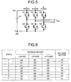
- FIG. 5 is a circuit diagram showing a basic structure of a three-phase voltage inverter for use in the embodiment as a power converter driven by PWM control.
- Fig. 6 is a drawing for explaining a relation between turned-on IGBT elements and voltage vectors in eight control states of the inverter shown in Fig. 5 .
- Fig. 7 is a drawing for explaining voltage vectors.
- Fig. 8 is a drawing for explaining a relation between phases and voltage vectors.
- the three-phase voltage inverter has a structure in which three sets of semiconductor switching elements, (Q1, Q4), (Q3, Q6) (Q5, Q2), that are connected to each other in series are connected in parallel to a direct-current power supply 15.
- Each semiconductor switching element has incorporated therein or has mounted thereon a flywheel diode.
- Each semiconductor switching element may be, for example, an IGBT element, and is hereinafter referred to as an IGBT element.
- the IGBT elements (Q1, Q4) are in u phase
- the IGBT elements (Q3, Q6) are in v phase
- the IGBT elements (Q5, Q2) are in w phase. From the respective connection ends, three-phase voltages uvw are extracted.
- each phase has two states, in which upper-arm IGBT elements (Q1, Q3, Q5) connected to the positive pole of the direct-current power supply 15 are turned on or lower-arm IGBT elements (Q4, Q6, Q2) connected to the negative pole thereof are turned on.
- upper-arm IGBT elements Q1, Q3, Q5
- lower-arm IGBT elements Q4, Q6, Q2
- Fig. 6 is a drawing for explaining a relation among these eight states, turned-on IGBT elements, and voltage vectors output from the three-phase inverter.
- the voltage vector V0 is a vector when IGBT elements (Q4, Q6, and Q2) are turned on.
- the voltage vector V1 is a vector when IGBT elements (Q1, Q6, and Q2) are turned on.
- the voltage vector V2 is a vector when IGBT elements (Q1, Q3, and Q2) are turned on.
- the voltage vector V3 is a vector when IGBT elements (Q4, Q3, and Q2) are turned on.
- the voltage vector V4 is a vector when IGBT elements (Q4, Q3, and Q5) are turned on.
- the voltage vector V5 is a vector when IGBT elements (Q4, Q6, and Q5) are turned on.
- the voltage vector V6 is a vector when IGBT elements (Q1, Q6, and Q5) are turned on.
- the voltage vector V7 is a vector when IGBT elements (Q1, Q3, and Q5) are turned on.
- each phase and each of the voltage vectors V0 to V7 is as shown in Fig. 7 .
- the voltage vectors V1 to V6 have a phase difference from one another by ⁇ /3 radian, and their magnitude is equal to the voltage Vdc of the direct-current power supply 15.
- the voltage vectors V0 and V7 are vectors each having a magnitude of 0, and are referred to as zero-voltage vectors.
- the phase of the voltage vector V1 coincides with the u phase
- the phase of the voltage vector V3 coincides with the v phase
- the phase of the voltage vector V5 coincides with the w phase.
- the voltage-vector control unit 11 selects a type of combination of the voltage vectors V0 to V7 and determines the output times.
- Vw a ⁇ Vdc 3 ⁇ sin ⁇ + 2 3 ⁇ ⁇
- the phase ⁇ in equations (1) is increased with time, but can be considered as being constant during the PWM control cycle T, which is a short cycle.
- the phase ⁇ has six ranges, that is, 0 ⁇ /3, ⁇ /3 ⁇ 2 ⁇ /3, 2 ⁇ /3 ⁇ , ⁇ 4 ⁇ /3, 4 ⁇ /3 ⁇ 5 ⁇ /3, and 5 ⁇ /3 ⁇ 2 ⁇ .
- the number of voltage vectors to be selected is four out of eight, but the combination of them varies for each range of the phase ⁇ .
- the zero-voltage vectors V0 and V7 are always included in any combination.
- the output state of the voltage-vector control unit 11 shown in Fig. 4 represents an output state in which the phase ⁇ in the PWM control cycle T is within a range of 0 ⁇ /3, which is hereinafter used for description.
- the time for outputting the selected voltage vector can be found in equations (2) by using, in place of ⁇ , the remainder obtained by dividing ⁇ by ⁇ /3.
- FIG. 9 is a flowchart for explaining the operation of the voltage-vector adjusting unit shown in Fig. 4 .
- Figs. 10A to 10C are diagrams for explaining loci of magnetic flux vectors when the voltage vectors are adjusted.
- the voltage-vector adjusting unit 12 reads the output times t1, t2, t0, and t7 of the voltage vectors output from the voltage-vector control unit 11 (step ST10), and then determines whether a total output time t0+t7 of the zero-voltage vectors is longer than a minimum zero-voltage-vector output time Tz (step ST11).
- step ST11 the total output time t0+t7 of the zero-voltage vectors is longer than the minimum zero-voltage-vector output time Tz (step ST11: No)
- the read output times t1, t2, t0, and t7 are directly taken as t1', t2', t0', and t7' (step ST12).
- step ST14 the output times t0', t1', t2', and t7' of the voltage vectors V0, V1, V2, and V7 adjusted at either one of steps ST12 and ST13 are output to the firing-pulse generating unit 13 (step ST14).
- the voltage vectors V0, V1, V2, and V7 selected by the voltage-vector control unit 11 are used as they are for output to the firing-pulse generating unit 13.
- a locus of a magnetic flux vector obtained through integration of the voltages can be drawn as shown in Figs. 10A to 10C .
- Fig. 10A a locus A of a magnetic flux vector for one PWM control cycle before adjustment of the voltage vectors is depicted.
- Fig. 10B a locus A' of the magnetic flux vector after adjustment of the voltage vectors is depicted.
- the locus A' is shorter than the previous one.
- Fig. 10C is drawn by overlaying Figs. 10A and 10B each other.
- magnetic flux vectors ⁇ 0 and ⁇ 7 are magnetic flux vectors corresponding to the zero-voltage vectors V0 and V7. Since the zero-voltage vectors V0 and V7 do not have a magnitude, the magnetic flux vectors ⁇ 0 and ⁇ 7 each stay at one point even with time.
- a magnetic flux vector ⁇ 1 is a magnetic flux vector corresponding to the voltage vector V1.
- the magnitude of the magnetic flux vector ⁇ 1 is the product of the magnitude of the voltage vector V1 and its output time.
- a magnetic flux vector ⁇ 2 is a magnetic flux vector corresponding to the voltage vector V2.
- the magnitude of the magnetic flux vector ⁇ 2 is the product of the magnitude of the voltage vector V2 and its output time. As with the voltage vectors V1 and V2, the magnetic flux vectors ⁇ 1 and ⁇ 2 have a phase difference of ⁇ /3 radian.
- the locus A and A' of the magnetic flux vectors are in the order of ⁇ 0 ⁇ 1 ⁇ 2 ⁇ 7.
- the load is an induction motor
- the magnetic flux vectors are equivalent to stator magnetic fluxes. Therefore, the type of the voltage vectors and their output times are selected so that the locus A of the magnetic flux before the voltage-vector adjusting unit 12 adjusts the voltage vectors smoothly goes along an arc. Even after the voltage vectors are adjusted by the voltage-vector adjusting unit 12, it is required that the locus A' of the magnetic flux smoothly goes along the arc.
- a triangle formed by connecting a start point and an end point of the locus A' together in the PWM control cycle T is similar to a triangle formed by connecting a start point and an end point of the locus A together.
- the end point of the locus A' is present on the arc, as is the case of the locus A. Therefore, if the voltage vectors are adjusted with the relative ratio between the output times of the voltage vectors V1 and V2 being unchanged, the locus A' of the magnetic flux after adjustment can also be made to smoothly go along the arc.
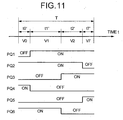
- Fig. 11 is a time chart for explaining the operation of the firing-pulse generating unit shown in Fig. 4 .
- the firing-pulse generating unit 13 generates on-off signals PQ1 to PQ6 of the respective IGBT elements from the voltage vectors V1, V2, V0, and V7, which are output from the voltage-vector adjusting unit 12, and the adjusted output times t1', t2', t0', and t7' of the voltage vectors. That is, the relation between the voltage vectors and the IGBT elements is shown in Fig. 6 . As shown in Fig.
- the on-off signals PQ1 to PQ6 for the IGBT elements Q1 to Q6 can be generated.
- Figs. 12A to 12D are drawings for explaining a relation between the progression of the voltage vectors and line-to-line voltages.
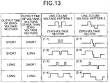
- Fig. 13 is a drawing that depicts line-to-line voltage patterns extracted in view of a pulse polarity, an output time of the zero-voltage vectors, and output times of voltage vectors other than the zero-voltage vectors.
- Figs. 12A to 12D are drawings depicting the four types of progression of the voltage vectors shown above with line-to-line voltage waveforms. It is understood from Figs. 12A to 12D that a pulse of a line-to-line voltage may be changed around the zero-voltage vector in the same polarity or may be changed around the zero-voltage vector in different polarities.
- Fig. 13 is a drawing that depicts line-to-line voltage patterns extracted from this Figs. 12A to 12D in view of a pulse polarity, an output time of the zero-voltage vectors, and output times of voltage vectors other than the zero-voltage vectors. In Fig.
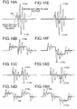
- Figs. 14A to 14H depicts the magnitude of each surge voltage occurring in the changes in line-to-line voltage shown in Fig. 13 .
- Figs. 14A to 14H as for Figs. 14C, 14D, 14G and 14H where the zero-voltage-vector output time is long, no surge voltage exceeding twice the direct-current bus voltage Vdc occurs.
- Figs. 14A, 14B, 14E and 14F where the zero-voltage-vector output time is short, a surge voltage exceeding twice the direct-current bus voltage Vdc occurs. It is therefore understood that appropriate selection of the output time of the zero-voltage vectors can suppress the occurrence of a surge voltage exceeding twice the direct-current bus voltage Vdc.
- a zero-voltage-vector output time always equal to or larger than a predetermined value can be achieved. Therefore, a resonant phenomenon associated with switching of the IGBT elements can be attenuated while the zero-voltage vectors are being output, thereby effectively suppressing a surge voltage exceeding twice the direct-current bus voltage Vdc.
- the adjustment of the voltage-vector output times is performed on the output times of the voltage vectors that are parameters generated based on three-phase voltage instructions and are common to three phases. Therefore, with one adjustment, an effect of suppressing a surge voltage can be obtained over all phases. Also, with the contrivance in the adjustment of the voltage vectors, fluctuations in the locus of the magnetic flux vector associated with suppression of a surge voltage can be minimized.
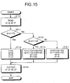
- Fig. 15 is a flowchart for explaining the operation of a voltage-vector adjusting unit included in a controlling device for the power controller according to a second embodiment of the present invention.
- the voltage-vector adjusting unit 12 adjusts the output times of the voltage vectors output from the voltage-vector control unit 11 according to a procedure shown in Fig. 15 , where an adjusting operation is performed for both of a case of ensuring the zero-voltage-vector output time to be equal to or larger than a predetermined value and a case of making the zero-voltage-vector output time zero.
- FIG. 15 With reference to Fig. 15 , the operation of the voltage-vector adjusting unit 12 according to the second embodiment is described below.
- Fig. 15 procedures identical to those shown in Fig. 9 are provided with the same reference numerals.
- description is made mainly to portions specific to the second embodiment.
- step ST11 when the total zero-voltage-vector output time t0+t7 is shorter than the minimum zero-voltage-vector output time Tz (step ST11: No), it is further determined according to the second embodiment whether the total zero-voltage-vector output time t0+t7 is longer than 1/2 of the minimum zero-voltage-vector output time Tz (step ST20).
- step ST14 the output times t0', t1', t2', and t7' of the voltage vectors V0, V1, V2, and V7 adjusted at any one of the steps ST12, ST13, and ST21 are output to the firing-pulse generating unit 13.
- the voltage vectors V0, V1, V2, and V7 selected by the voltage-vector control unit 11 are used as they are for output to the firing-pulse generating unit 13.
- the total zero-voltage-vector output time t0+t7 is shorter than the minimum zero-voltage-vector output time Tz
- whether to provide a zero-voltage-vector output time equal to or larger than a predetermined value or to make the zero-voltage-vector output time zero can be selected based on the concept of rounding-off, thereby suppressing a surge voltage exceeding twice the direct-current bus voltage Vdc.
- the adjustment of the voltage-vector output times is performed on the output times of the voltage vectors, which are parameters that are generated based on three-phase voltage instructions and are common to three phases. Therefore, with one adjustment, an effect of suppressing a surge voltage can be obtained over all phases. Furthermore, with the contrivance in the adjustment of the voltage vectors, fluctuation in the locus of the magnetic flux vector associated with suppression of a surge voltage can be minimized.
- the boundary for determining whether the total zero-voltage-vector output time t0+t7 is set as the minimum zero-voltage-vector output time Tz or 0 is Tz/2.
- the boundary is not restricted to Tz/2 and can be arbitrarily set in a range of 0 to Tz.
- the first embodiment represents an example in which, with zero being taken as the boundary, the total zero-voltage-vector output time is rounded up to the minimum zero-voltage-vector output time Tz.
- Fig. 16 is a block diagram depicting the structure of a power-converter control apparatus according to a third embodiment of the present invention.
- components are similar to those in the first embodiment, but an exemplary structure is depicted in which, for example, two PWM control cycles are taken as a unit for control.
- the concept of the control phase ⁇ is similar to that in the first embodiment.
- a voltage-vector control unit 21 selects, from out of voltage instruction values Vu, Vv, and Vw of the respective phases of the power converter, voltage vectors to be output from the power converter within two control cycles of PWM control (in an example shown in the drawing, (V0_1, V1_1, V2_1, V7_1)(V0_2, V1_2, V2_2, V7_2)), and calculates their output times (t0_1, t1_1, t2_1, t7_1)(t0_2, t1_2, t2_2, t7_2).
- a voltage-vector adjusting unit 22 outputs the voltage vectors input from the voltage-vector control unit 21 (in the example shown in the drawing, (V0_1, V1_1, V2_1, V7_1)(V0_2, V1_2, V2_2, V7_2)) as they are in a method described further below ( Fig.
- a firing-pulse generating unit 23 generates, based on the voltage vectors input from the voltage-vector adjusting unit 22 and the voltage-vector output times adjusted at the voltage-vector adjusting unit 22, on-off signals "PQ1, PQ2, PQ3, PQ4, PQ5, and PQ6" for semiconductor switching elements that form the power converter.
- the voltage-vector control unit 21 and the firing-pulse generating unit 23 perform operations of the voltage-vector control unit 11 and the firing-pulse generating unit 13 according to the first embodiment ( Fig. 4 ) merely as being extended for two PWM control cycles, and therefore are not described in detail.
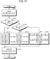
- Fig. 17 is a flowchart showing the voltage-vector adjusting unit 22 shown in Fig. 16 .
- the voltage-vector adjusting unit 22 reads output times (t0_1, t1_1, t2_1, t7_1) and (t0_2, t1_2, t2_2, t7_2) of the voltage vectors output from the voltage-vector control unit 21 (step ST31), and then it is determined whether either one or both of the total zero-voltage-vector output times (t0_1+t7_1) and (t0_2+t7_2) in each cycle are longer than the minimum zero-voltage-vector output time Tz (step ST32).
- step ST32 when both of the total zero-voltage-vector output times (t0_1+t7_1) and (t0_2+t7_2) in each cycle are longer than the minimum zero-voltage-vector output time Tz (step ST32: Yes), the read output times t1_1, t2_1, t0_1, t7_1, t1_2, t2_2, t0_2, and t7_2 are directly taken as adjusted output times t1_1', t2_1', t0_1', t7_1', t1_2', t2_2', t0_2', and t7_2' (step ST33).
- step ST32 when either or both of the total zero-voltage-vector output times (t0_1+t7_1) and (t0_2+t7_2) in each cycle are shorter than the minimum zero-voltage-vector output time Tz (step ST32: No), it is determined whether a total of the output times of the zero-voltage vectors over two cycles (t0_1+t7_1+t0_2+t7_2) is longer than the minimum zero-voltage-vector output time Tz (step . ST34).
- step ST34 the total of the output times of the zero-voltage vectors over two cycles (t0_1+t7_1+t0_2+t7_2) is longer than the minimum zero-voltage-vector output time Tz (step ST34: Yes)
- the voltage vectors V0_1, V1_1, V2_1, V7_1, V0_2, V1_2, V2_2, and V7_2 selected by the voltage-vector control unit 21 for two cycles are used as they are for output to the firing-pulse generating unit 23.
- two PWM control cycles are taken as a unit for adjusting the voltage vectors.
- the output times of the zero-voltage vectors located at both ends of each cycle being made zero, the remaining output time of the zero-voltage vectors can be doubled. Consequently, for one PWM control cycle, the total of the output times of the non-zero-voltage vectors does not have to be changed until the total of the output times of the zero-voltage vectors becomes less than 1/2 of the minimum zero-voltage-vector output time Tz, thereby reducing error.
- the zero-voltage-vector output time is ensured to be equal to or larger than the minimum zero-voltage-vector output time, or zero. Therefore, a surge voltage exceeding twice the direct-current bus voltage Vdc can be suppressed.
- the adjustment of the voltage-vector output times is performed on the output times of the voltage vectors, which are parameters that are generated based on three-phase voltage instructions and are common to three phases. Therefore, with one adjustment, an effect of suppressing a surge voltage can be obtained over all phases. Furthermore, with the contrivance in the adjustment of the voltage vectors, fluctuations in the locus of the magnetic flux vector associated with suppression of a surge voltage can be minimized.
- the voltage-vector output times are adjusted for two PWM control cycles.
- the cycles for adjustment are not particularly restricted to two cycles. It goes without saying that the cycles may be arbitrarily set in a range of equal to or more than two cycles.
- Fig. 18 is a flowchart for explaining the operation of a voltage-vector adjusting unit included in a power-converter control apparatus according to a fourth embodiment of the present invention.
- the voltage-vector adjusting unit 22 according to the fourth embodiment adjusts the output times of the voltage vectors output from the voltage-vector control unit 21 according to a procedure shown in Fig. 18 , where, in a predetermined case, an adjusting operation is performed, such as collecting the output times of the same voltage vectors in the two cycles as one.
- the voltage vectors V0_1, V1_1, V2_1, V7_1, V0_2, V1_2, V2_2, and V7_2 selected by the voltage-vector control unit 21 for two cycles are used as they are for output to the firing-pulse generating unit 23.
- the fourth embodiment when the voltage vectors are adjusted by taking two PWM control cycles as a unit, output times of same voltage vectors in the two control cycles are collected as one, thereby doubling the output times of the voltage vectors including the zero-voltage vectors. Consequently, for one PWM control cycle, the total of the output times of the voltage vectors other than the zero-voltage vectors does not have to be changed until the total of the output times of the zero-voltage vectors becomes less than 1/2 of the minimum zero-voltage-vector output time Tz, thereby reducing error. According to this method, the zero-voltage-vector output time is always ensured, and therefore a surge voltage exceeding twice the direct-current bus voltage Vdc can be suppressed.
- the adjustment of the voltage-vector output times is performed on the output times of the voltage vectors, which are parameters that are generated based on three-phase voltage instructions and are common to three phases. Therefore, with one adjustment, an effect of suppressing a surge voltage can be obtained over all phases. Furthermore, with the contrivance in the adjustment of the voltage vectors, fluctuations in the locus of the magnetic flux vector associated with suppression of a surge voltage can also be minimized.
- the voltage-vector output times are adjusted for two PWM control cycles.
- the cycles for adjustment are not particularly restricted to two cycles. It goes without saying that the cycles may be arbitrarily set in a range of equal to or more than two cycles.
- Fig. 19 is a block diagram showing a power-converter control apparatus according to a fifth embodiment of the present invention.
- procedures identical to those shown in Fig. 4 are provided with the same reference numerals.
- description is made mainly to portions specific to the fifth embodiment.
- a voltage-vector adjusting unit 31 is provided in place of the voltage-vector adjusting unit 12, and a delay unit 32 is added.
- the delay unit 32 gives the voltage vectors adjusted and output by the voltage-vector adjusting unit 31 and their output times to the voltage-vector adjusting unit 31 with a delay of one cycle.
- the delay unit 32 gives voltage vectors V0_p, V1_p, V2_p, and V7_p with a delay of one cycle and output times t0_p, t1_p, t2_p, and t7_p with a delay of one cycle to the voltage-vector adjusting unit 31.
- the voltage-vector adjusting unit 31 adjusts and outputs the output times of the voltage vectors output from the voltage-vector control unit 11 so that the zero-voltage-vector output time is equal to or larger than a predetermined value. At this time, the adjusted times in one previous PWM control cycle obtained through the delay unit 32 are also used for adjustment.
- FIG. 20 is a flowchart for explaining the operation of the voltage-vector adjusting unit 31 shown in FIG. 19 .
- procedures identical or equivalent to the procedures shown in Fig. 9 are provided with the same reference numerals.
- the voltage-vector adjusting unit 31 reads output times t1, t2, t0, and t7 of voltage vectors input from the voltage-vector control unit 11, voltage vectors V1_p, V2_p, V0_p, and V7_p, which are adjusted outputs in one previous PWM control cycle that are input from the delay unit 32, and their output times t1_p, t2_p, t0_p, and t7_p (step ST51). Since the output time of the zero-voltage vectors may be zero, it is determined whether the vector last outputted in the previous time (in one previous PWM control cycle) is a zero-voltage vector (step ST52).
- step ST52 when the vector last output in the previous time is a zero-voltage vector (step ST52: Yes), the procedure branches to a sequence in which the process is started with the zero-voltage vector, and it is determined whether a total of output times of the zero-voltage vectors t0+t7 is longer than the minimum zero-voltage-vector output time Tz (step ST11).
- step ST11 When the total of output times of the zero-voltage vectors t0+t7 is longer than the minimum zero-voltage-vector output time Tz (step ST11: Yes), the output times t1, t2, t0, and t7 at the present time are directly taken as adjusted output times t1', t2', t0', and t7' (step ST12).
- step ST11 when the total of output times of the zero-voltage vectors t0+t7 is shorter than the minimum zero-voltage-vector output time Tz (step ST11: Yes), it is determined whether the total zero-voltage-vector output time t0+t7 is longer than 1/2 of the minimum zero-voltage-vector output time Tz (step ST53).
- step ST52 when the vector last output at the previous time is not a zero vector (step ST52: No), the procedure branches to a sequence in which the procedure starts with a non-zero-voltage vector.
- step ST14 the output times t0', t1', t2', and t7' of the voltage vectors V0, V1, V2, and V7 adjusted at any one of steps ST12, ST54, ST55, ST57, and ST58 are output to the firing-pulse generating unit 13 (step ST14).
- the voltage vectors V0, V1, V2, and V7 selected by the voltage-vector control unit 11 are used as they are for output to the firing-pulse generating unit 13.
- the zero-voltage vectors located at the first and last of the pulse-width control cycle are combined as one, thereby doubling the output times of the zero-voltage vectors. Consequently, the total of the output times of the non-zero-voltage vectors does not have to be changed until the total of the output times of the zero-voltage vectors becomes less than the minimum zero-voltage-vector output time Tz, thereby reducing error.
- the zero-voltage-vector output time is ensured to be equal to or larger than the minimum zero-voltage-vector output time, or is made zero. Therefore, a surge voltage exceeding twice the direct-current bus voltage Vdc can be suppressed.
- the adjustment of the voltage-vector output times is performed on the output times of the voltage vectors, which are parameters that are generated based on three-phase voltage instructions and are common to three phases. Therefore, with one adjustment, an effect of suppressing a surge voltage can be obtained over all phases. Furthermore, with the contrivance in the adjustment of the voltage vectors, fluctuations in the locus of the magnetic flux vector associated with suppression of a surge voltage can also be minimized.
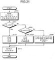
- Fig. 21 is a flowchart for explaining the operation of a voltage-vector adjusting unit included in a power-converter control apparatus according to a sixth embodiment of the present invention.
- the voltage-vector adjusting unit 31 according to the sixth embodiment performs an adjusting operation by using an output time of a zero-voltage vector last output in the previous PWM control cycle to determine an output time of a zero-voltage vector to be first output in the present PWM control cycle.
- the operation of the voltage-vector adjusting unit 31 according to the sixth embodiment is described below.
- procedures identical to those shown in Fig. 20 are provided with the same reference numerals.
- description is made mainly to portions specific to the sixth embodiment.
- the voltage-vector adjusting unit 31 determines whether a total of an output time t0_p of a zero-voltage vector last output at the previous time (at one previous PWM control cycle) and an output time t0 of a zero-voltage vector to be first output at this time is longer than the minimum zero-voltage-vector output time Tz (step ST61).
- step ST61 when the total zero-voltage-vector output time t0_p+t0 is longer than the minimum zero-voltage-vector output time Tz (step ST61: Yes), the output times t1, t2, t0, and t7 at this time are directly taken as adjusted output times t1', t2', t0', and t7' (step ST12).
- step ST61 when the total zero-voltage-vector output time t0_p+t0 is shorter than the minimum zero-voltage-vector output time Tz (step ST61: No), it is further determined whether a total zero-voltage-vector output time t0_p+t0+t7 is longer than the minimum zero-voltage-vector output time Tz (step ST62).
- step ST14 the output times t0', t1', t2', and t7' of the voltage vectors V0, V1, V2, and V7 adjusted at any one of steps ST12, ST63, and ST64 are output to the firing-pulse generating unit 13 (step ST14).
- the voltage vectors V0, V1, V2, and V7 selected by the voltage-vector control unit 11 are used as they are for output to the firing-pulse generating unit 13.
- an output time of a zero-voltage vector to be output in the present PWM control cycle is determined. Therefore, the output time of the zero-voltage vector can be ensured even when the zero-voltage vector extends over the PWM control cycles. Therefore, a surge voltage exceeding twice the direct-current bus voltage Vdc can be suppressed.
- the adjustment of the voltage-vector output times is performed on the output times of the voltage vectors, which are parameters that are generated based on three-phase voltage instructions and are common to three phases. Therefore, with one adjustment, an effect of suppressing a surge voltage can be obtained over all phases. Furthermore, with the contrivance in the adjustment of the voltage vectors, fluctuations in the locus of the magnetic flux vector associated with suppression of a surge voltage can also be minimized.
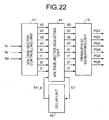
- Fig. 22 is a block diagram depicting the structure of a power-converter control apparatus according to a seventh embodiment of the present invention.
- Fig. 22 procedures identical to those shown in Fig. 4 are provided with the same reference numerals.
- description is made mainly to portions specific to the seventh embodiment.
- a voltage-vector adjusting unit 41 is provided in place of the voltage-vector adjusting unit 12, and a delay unit 42 is added.
- the voltage-vector adjusting unit 41 adjusts and outputs the output times of the voltage vectors output from the voltage-vector control unit 11 so that the zero-voltage-vector output time is equal to or larger than a predetermined value.
- the voltage-vector adjusting unit 41 has a function of outputting an error Err associated with adjustment, and uses an error Err_p input through the delay unit 42 in one previous PWM control cycle for adjustment of the voltage vectors in one subsequent cycle.
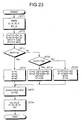
- Fig. 23 is a flowchart for explaining the operation of the voltage-vector adjusting unit 41 shown in Fig. 22 .
- Figs. 24A to 24C are drawings for explaining an error-calculating operation to be performed by the voltage-vector adjusting unit shown in Fig. 22 .
- the voltage-vector adjusting unit 41 reads the output times t1, t2, t0, and t7 of the voltage vectors output from the voltage-vector control unit 11 together with the error Err_p calculated at previous time (in one previous PWM control cycle) (step ST71), and corrects the output times t1, t2, t0, and t7 of the voltage vectors so that the previous error Err_p is corrected (step ST72).
- step ST72 the output time t1 is corrected to t1(1+Err_p).
- the output time t2 is corrected to t2(1+Err_p).
- the output times t0 and t7 are corrected to (T-t1-t2)/2.
- the minimum zero-voltage-vector output time Tz is ensured, or the zero-voltage-vector output time is deleted (steps ST11 to ST21).
- Fig. 24A loci A and B of magnetic flux vectors for two PWM control cycles before voltage vector adjustment are shown.
- the locus A is in the previous cycle, while the locus B is the current cycle.
- Fig. 24B loci A' and B' of magnetic flux vectors after voltage vector adjustment are shown.
- Fig. 24C is drawn by overlaying Figs. 24A and 24B each other.
- the loci A and B can be considered as being different from the loci A' and B' only in dividing ratio of dividing the straight line, that is, the arc, into two.
- the dividing ratio between the locus A and the locus B before adjustment is 1:1.
- the shortened portion of the locus A' is added to the locus B' to equalize the total values, only the ratio between the locus A and the locus A' is required to be known. Therefore, an error Err obtained from any one of the following equations (7) to (9) are used.
- the adjustment error can be corrected. Therefore, a surge voltage exceeding twice the direct-current bus voltage Vdc can be reliably suppressed. Also, fluctuations in the locus of the magnetic flux vector associated with suppression of a surge voltage can be minimized. Furthermore, the adjustment of the voltage-vector output times is performed on the output times of the voltage vectors, which are parameters that are generated based on three-phase voltage instructions and are common to three phases. Therefore, with one adjustment, an effect of suppressing a surge voltage can be obtained over all phases.
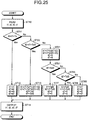
- Fig. 25 is a flowchart for explaining the operation of a voltage-vector adjusting unit included in a power-converter control apparatus according to an eighth embodiment of the present invention.
- Fig. 25 procedures identical or equivalent to those shown in Fig. 9 (the first embodiment) are provided with the same reference numerals.
- description is made mainly to portions specific to the eighth embodiment.
- the eighth embodiment describes an exemplary measure (steps ST81 to ST85) to details (inconveniences) taken as an exception and not considered in the power-converter control apparatus shown in the first embodiment ( Fig. 4 ) when the output times of the zero-voltage vectors are adjusted to zero as described in the second embodiment ( Fig. 15 ).
- step ST81 when the zero-voltage-vector output time is adjusted to zero (step ST21), it is determined whether the adjusted output time t1' of the voltage vector V1 is shorter than 1/2 of the minimum zero-voltage-vector output time Tz (step ST81).
- step ST81 when the adjusted output time t1' of the voltage vector V1 is longer than 1/2 of the minimum zero-voltage-vector output time Tz (step ST81: No), it is determined whether the adjusted output time t2' of the voltage vector V2 is shorter than 1/2 of the minimum zero-voltage-vector output time Tz (step ST83).
- step 83 when the adjusted output time t2' of the voltage vector V2 is longer than 1/2 of the minimum zero-voltage-vector output time Tz (step 83: No), the output times t1', t2', t0', and t7' adjusted at step ST11 to ST21 are not readjusted (step ST85).
- the eighth embodiment it is possible to restrict a surge voltage that may occur regarding the output times of the voltage vectors other than the zero-voltage vectors when the output time of the zero-voltage vectors are adjusted to be zero.
- a surge voltage exceeding twice the direct-current bus voltage Vdc can be reliably suppressed.
- an effect of such suppression of a surge voltage can be obtained over all phase only by adjusting the voltage-vector output times, which are parameters that are common to three phases.
- fluctuations in the locus of the magnetic flux vector associated with suppression of a surge voltage can be minimized.
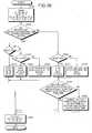
- Fig. 26 is a flowchart for explaining the operation of a voltage-vector adjusting unit included in a power-converter control apparatus according to a ninth embodiment of the present invention.
- procedures identical or equivalent to those shown in Fig. 20 (the fifth embodiment) are provided with the same reference numerals.
- description is made mainly to portions specific to the ninth embodiment.
- the ninth embodiment describes an exemplary measure (steps ST90 to ST93) to details (inconveniences) taken as an exception and not considered in the power-converter control apparatus shown in the fifth embodiment ( Fig. 19 ) when the output times of the zero-voltage vectors are adjusted to zero as described in Fig. 20 .
- step ST90 in place of the first step ST51 shown in Fig. 20 , the voltage vectors V1, V2, V0, and V7 input from the voltage-vector control unit 11, the output times t1, t2, t0, and t7, the voltage vectors V1_p, V2_p, V0_p, and V7_p, which are adjusted outputs input from the delay unit 32 at one previous PWM control cycle, and their output times t1_p, t2_p, t0_p, and t7_p are read. Then, when the output times of the zero-voltage vectors are adjusted to zero at step ST57 or ST 58, it is determined whether the voltage vector last output at the previous time is identical to the voltage vector to be first output at this time (step ST91).
- step ST91: Yes when the voltage vector last output at the previous time is identical to the voltage vector to be first output at the present time (step ST91: Yes), this is the case of (3)' described above, and therefore no process is performed and then the procedure goes to step ST93.
- step ST91: No when the voltage vector last output at the previous time is different from the voltage vector to be first output at this time (step ST91: No), this is the case of (4)'. Therefore, the voltage vector to be first output at the present time is changed to the vector last output at the previous time (step ST92), and the procedure goes to step ST93.
- step ST93 the adjusted output times t1', t2', t0', and t7' of the voltage vectors and the voltage vectors V1', V2', V0', and V7' are output.
- the voltage vectors V0, V1 , V2, and V7 selected by the voltage vector controlling unit 11 are directly output as the voltage vectors V0', V1', V2', and V7' to the firing-pulse generating unit 13.
- Figs. 14E and 14F the cases of Figs. 14E and 14F occurring when the output times of the zero-voltage vectors are adjusted to zero can be avoided. Therefore, a surge voltage exceeding twice the direct-current bus voltage Vdc can be reliably suppressed. Also, an effect of such suppression of a surge voltage can be obtained over all phase only by adjusting the voltage-vector output times, which are parameters that are common to three phases.
- a surge voltage exceeding twice the direct-current bus voltage Vdc can be suppressed by at least ensuring the output time of the zero-voltage vectors equal to or larger than a predetermined value or by making the output time zero.
- the adjustment of the voltage-vector output times is performed on the output times of the voltage vectors, which are parameters that are generated based on three-phase voltage instructions and are common to three phases. Therefore, with one adjustment, an effect of suppressing a surge voltage can be obtained over all phases. Also, with the contrivance in the adjustment of the voltage vectors, fluctuations in the locus of the magnetic flux vector associated with suppression of a surge voltage can be minimized.
- a surge voltage exceeding twice the direct-current bus voltage Vdc can be suppressed by at least ensuring the output time of the zero-voltage vectors equal to or larger than a predetermined value or by making the output time zero.
- the adjustment of the voltage-vector output times is performed on the output times of the voltage vectors, which are parameters that are generated based on three-phase voltage instructions and are common to three phases. Therefore, with one adjustment, an effect of suppressing a surge voltage can be obtained over all phases.
- the present invention is suitable as a power-converter control apparatus when a connection cable between the power converter and a load is long.
Landscapes
- Engineering & Computer Science (AREA)
- Power Engineering (AREA)
- Inverter Devices (AREA)
Description
- The present invention relates to a power-converter control apparatus driven by pulse width modulation (PWM) control and, particularly, a controlling device that suppresses an abnormally high voltage (hereinafter, "surge voltage") occurring at a cable-connection end of a load when a connection cable between the power converter and the load is long.
-
Fig. 1 is a drawing for explaining a connection cable between an inverter, which is a power converter driven by PWM control, and a motor. InFig. 1 , aninverter 1, which is a power converter, has connected thereto amotor 2 via acable 3. In theinverter 1, a switching operation of semiconductor switching elements (for example, IGBT elements) is controlled through PWM control by a controlling unit not shown to generate three-phase voltages (uvw) varying stepwise from a direct-current power supply having a voltage Vdc, and these voltages are output to themotor 2 via theconnection cable 3. - Here, when this
connection cable 3 between theinverter 1 and themotor 2 is long, a surge voltage exceeding twice a direct-current bus voltage Vdc may occur at cable-connection ends of themotor 2. That is, theconnection cable 3 can be considered as a resonant circuit composed of a wiring inductance and a floating capacitance. When theconnection cable 3 is long, the wiring inductance and the floating inductance are both increased, thereby reducing a resonant frequency of the resonant circuit. As a result, before resonance excited at the resonant circuit due to a stepwise change in voltage produced by theinverter 1 is attenuated, the next stepwise change in voltage is applied. Such repeated application increases resonance, thereby causing a surge voltage, which is a voltage higher than usual, at the cable connection ends of themotor 2. - With reference to
Figs. 2A and3B , details of the surge voltage occurring at the cable connection ends of themotor 2 are described.Figs. 2A and3B are drawings that depict line-to-line voltage waveforms at both ends of theconnection cable 3 shown inFig. 1 . -
Fig. 2A depicts a case where an inverter-end line-to-line voltage Vuv_inv is varied stepwise as Vdc→0→Vdc. At this time, when a pulse width in voltage change coincides with half of a resonant cycle, as shown inFig. 2B , a motor-end line-to-line voltage Vuv_motor becomes three times as high as the direct-current bus voltage Vdc at maximum. - Also,
Fig. 3A depicts a case where the inverter-end line-to-line voltage Vuv_inv is varied stepwise as 0→Vdc→-Vdc→0. At this time, as shown inFig. 3B , the motor-end line-to-line voltage Vuv_motor becomes four times as high as the direct-current bus voltage Vdc at maximum. - From the description with reference to
Figs. 2A and3B , it is known that if the pulse width in voltage change is sufficiently large, after resonance occurring due to a stepwise voltage change is attenuated, the next stepwise voltage change is applied, and therefore a surge voltage exceeding twice the direct-current bus voltage Vdc does not occur. - To solve this surge-voltage problem, for example, first and second patent documents disclose a technology of monitoring a firing pulse width of each of IGBT elements, which serves as a line-to-line voltage pulse width of the inverter and limiting a maximum value of the firing pulse width to be equal to or smaller than a predetermined value and a minimum value of the firing pulse width to be equal to or larger than a predetermined value. The first patent document:
US Patent No. 5671130 ; and the second patent document:US Patent No. 5990658 . - Also, for example, third and fourth patent documents disclose a technology of monitoring each phase-voltage instruction value input to the PWM controller and limiting a maximum value of each phase-voltage instruction value to be equal to or smaller than a predetermined value and a minimum value of each phase voltage to be equal to or larger than a predetermined value. The third patent document:
US Patent No. 5912813 ; and the fourth patent document:US Patent No. 6014497 . - However, the firing pulse width or the voltage instruction value varies for each phase. Therefore, the firing pulse width or the voltage instruction value is required to be limited individually for each phase. That is, to suppress a surge voltage exceeding twice the direct-current bus voltage Vdc by applying the technologies disclosed in the patent documents, if the firing pulse width of each IGBT element or the maximum and minimum values of each phase-voltage instruction value are limited, a plurality of controlling units that control the maximum and minimum values of each phase are required.
- Also, one problem of this configuration is that, when the firing pulse width or the voltage instruction value of one phase is limited, an influence on other phases cannot be considered. Moreover, in relation to this problem, there is another problem in which all phases cannot be collectively handled for optimal limitation.
- The present invention is devised in view of the above, and an object of the present invention is to provide a power-converter control apparatus, the device being capable of collectively handling all phases and optimally suppressing a surge voltage exceeding twice a direct-current bus voltage.
- It is an object of the present invention to solve at least the above problems in the conventional technology.
- An apparatus for controlling a power converter according to one aspect of the present invention includes a voltage-vector control unit that determines, based on a voltage instruction value for the power converter, a voltage vector output from the power converter in one control cycle of a pulse-width-modulation control and a time to output the voltage vector; a voltage-vector adjusting unit that adjusts the time to output the voltage vector in such a manner that a time to output a zero-voltage vector becomes longer than a fixed time or zero; and a firing-pulse generating unit that generates a signal for turning on and off a semiconductor switching element included in the power converter based on the time to output the voltage vector adjusted by the voltage-vector adjusting unit.
- The other objects, features, and advantages of the present invention are specifically set forth in or will become apparent from the following detailed description of the invention when read in conjunction with the accompanying drawings.
-
-
Fig. 1 is a drawing for explaining a connection cable between an inverter, which is a power converter driven by PWM control, and a motor;Figs. 2A and 2B are (first) drawings that illustrate line-to-line voltage waveforms between both ends of the connection cable shown inFig. 1 ;Figs. 3A and 3B are (second) drawings that illustrate line-to-line voltage waveforms between both the ends of the connection cable shown inFig. 1 ;Fig. 4 is a block diagram depicting the structure of a power-converter control apparatus according to a first embodiment of the present invention;Fig. 5 is a circuit diagram depicting a basic structure of a three-phase voltage inverter for use in the embodiment as the power converter driven by PWM control;Fig. 6 is a drawing for explaining a relation between turned-on IGBT elements and voltage vectors in eight control states of the inverter shown inFig. 5 ;Fig. 7 is a drawing for explaining voltage vectors;Fig. 8 is a drawing for explaining a relation between phases and voltage vectors;Fig. 9 is a flowchart for explaining the operation of a voltage-vector adjusting unit shown inFig. 4 ;Figs. 10A to 10C are diagrams for explaining loci of magnetic flux vectors when the n voltage vectors are adjusted;Fig. 11 is a time chart for explaining the operation of a firing-pulse generating unit shown inFig. 4 ;Figs. 12a to 12D are drawings for explaining a relation between the progression of the voltage vectors and line-to-line voltages;Fig. 13 is a drawing that depicts line-to-line voltage patterns extracted in view of a pulse polarity, an output time of zero-voltage vectors, and an output time of voltage vectors other than the zero-voltage vectors;Figs. 14A to 14H are drawings for explaining surge voltages occurring due to the line-to-line voltages shown inFig. 13 ;Fig. 15 is a flowchart for explaining the operation of a voltage-vector adjusting unit included in a controlling device for the power controller according to a second embodiment of the present invention;Fig. 16 is a block diagram depicting the structure of a power-converter control apparatus according to a third embodiment of the present invention;Fig. 17 is a flowchart showing a voltage-vector adjusting unit shown inFig. 16 ;Fig. 18 is a flowchart for explaining the operation of a voltage-vector adjusting unit included in a power-converter control apparatus according to a fourth embodiment of the present invention;Fig. 19 is a block diagram showing a power-converter control apparatus according to a fifth embodiment of the present invention;Fig. 20 is a flowchart for explaining the operation of a voltage-vector adjusting unit shown inFIG. 19 ;Fig. 21 is a flowchart for explaining the operation of a voltage-vector adjusting unit included in a power-converter control apparatus according to a sixth embodiment of the present invention;Fig. 22 is a block diagram depicting the structure of a power-converter control apparatus according to a seventh embodiment of the present invention;Fig. 23 is a flowchart for explaining the operation of a voltage-vector adjusting unit shown inFig. 22 ;Figs. 24A to 24C are drawings for explaining an error-calculating operation to be performed by the voltage-vector adjusting unit shown inFig. 22 ;Fig. 25 is a flowchart for explaining the operation of a voltage-vector adjusting unit included in a power-converter control apparatus according to an eighth embodiment of the present invention; andFig. 26 is a flowchart for explaining the operation of a voltage-vector adjusting unit included in a power-converter control apparatus according to a ninth embodiment of the present invention. - Exemplary embodiments of a power-converter control apparatus according to the present invention are described below in detail with reference to the accompanying drawings.
-
Fig. 4 is a block diagram depicting the structure of a power-converter control apparatus according to a first embodiment of the present invention. A controlling device shown inFig. 4 includes a voltage-vector control unit 11, a voltage-vector adjustingunit 12, and a firing-pulse generating unit 13. - The voltage-
vector control unit 11 selects, from out of voltage instruction values Vu, Vv, and Vw of the respective phases of a power converter, voltage vectors to be output from the power converter within one control cycle of PWM control (in an example shown in the drawing, V0, V1, V2, and V7), and calculates their output times (t0, t1, t2, t7). - The voltage-vector adjusting
unit 12 outputs the voltage vectors input from the voltage-vector control unit 11 (in the example show in the drawing, V0, V1, V2, V7) as they are, and also adjusts the output times (t0, t1, t2, t7) of these voltage vectors so that a zero-voltage-vector output time is equal to or larger than a predetermined value for output (t0', t1', t2', t7'). - The firing-
pulse generating unit 13 generates, based on the voltage vectors input from the voltage-vector adjustingunit 12 and the voltage-vector output times adjusted at the voltage-vector adjustingunit 12, on-off signals "PQ1, PQ2, PQ3, PQ4, PQ5 and PQ6 " for semiconductor switching elements that form the power converter. - A specific operation of each block is described below. First, with reference to
Figs. 5 to 8 , the operation of the voltage-vector control unit 11 is described. Here,Fig. 5 is a circuit diagram showing a basic structure of a three-phase voltage inverter for use in the embodiment as a power converter driven by PWM control.Fig. 6 is a drawing for explaining a relation between turned-on IGBT elements and voltage vectors in eight control states of the inverter shown inFig. 5 .Fig. 7 is a drawing for explaining voltage vectors.Fig. 8 is a drawing for explaining a relation between phases and voltage vectors. - As shown in
Fig. 5 , the three-phase voltage inverter has a structure in which three sets of semiconductor switching elements, (Q1, Q4), (Q3, Q6) (Q5, Q2), that are connected to each other in series are connected in parallel to a direct-current power supply 15. Each semiconductor switching element has incorporated therein or has mounted thereon a flywheel diode.
Each semiconductor switching element may be, for example, an IGBT element, and is hereinafter referred to as an IGBT element. In the example shown in the drawing, the IGBT elements (Q1, Q4) are in u phase, the IGBT elements (Q3, Q6) are in v phase, and the IGBT elements (Q5, Q2) are in w phase. From the respective connection ends, three-phase voltages uvw are extracted. - Here, as for an on-off control state of the IGBT elements, each phase has two states, in which upper-arm IGBT elements (Q1, Q3, Q5) connected to the positive pole of the direct-
current power supply 15 are turned on or lower-arm IGBT elements (Q4, Q6, Q2) connected to the negative pole thereof are turned on. For three phases, 2×2×2=8 states are present. -
Fig. 6 is a drawing for explaining a relation among these eight states, turned-on IGBT elements, and voltage vectors output from the three-phase inverter. InFig. 6 , the voltage vector V0 is a vector when IGBT elements (Q4, Q6, and Q2) are turned on. The voltage vector V1 is a vector when IGBT elements (Q1, Q6, and Q2) are turned on. The voltage vector V2 is a vector when IGBT elements (Q1, Q3, and Q2) are turned on. The voltage vector V3 is a vector when IGBT elements (Q4, Q3, and Q2) are turned on. The voltage vector V4 is a vector when IGBT elements (Q4, Q3, and Q5) are turned on. The voltage vector V5 is a vector when IGBT elements (Q4, Q6, and Q5) are turned on. The voltage vector V6 is a vector when IGBT elements (Q1, Q6, and Q5) are turned on. The voltage vector V7 is a vector when IGBT elements (Q1, Q3, and Q5) are turned on. - A relation between each phase and each of the voltage vectors V0 to V7 is as shown in
Fig. 7 . InFig. 7 , the voltage vectors V1 to V6 have a phase difference from one another by π/3 radian, and their magnitude is equal to the voltage Vdc of the direct-current power supply 15. The voltage vectors V0 and V7 are vectors each having a magnitude of 0, and are referred to as zero-voltage vectors. The phase of the voltage vector V1 coincides with the u phase, the phase of the voltage vector V3 coincides with the v phase, and the phase of the voltage vector V5 coincides with the w phase. - In the three-phase voltage inverter, by varying the type of combination of the voltage vectors V0 to V7 output during the PWM control cycle T and their output times, voltages each having and arbitrary magnitude and phase can be output on the average. The voltage-
vector control unit 11 selects a type of combination of the voltage vectors V0 to V7 and determines the output times. - It is assumed that the voltage instructions Vu, Vv, and Vw for each phase are given by equations (1).

- Selection of the type of combination of the voltage vectors V0 to V7 is performed as shown in
Fig. 8 according to the phase θ in the current PWM control cycle T. As shown inFig. 8 , the phase θ has six ranges, that is, 0≤θ<π/3, π/3≤θ<2π/3, 2π/3≤θ<π, π≤θ<4π/3, 4π/3≤θ<5π/3, and 5π/3≤θ<2π. The number of voltage vectors to be selected is four out of eight, but the combination of them varies for each range of the phase θ. However, the zero-voltage vectors V0 and V7 are always included in any combination. - In
Fig. 8 , when the phase θ in the current PWM control cycle T is within a range of 0≤θ<π/3, for example, the combination of voltage vectors to be selected is V1, V2, V0, and V7. Times t1, t2, t0, and t7 for outputting these selected voltage vectors V1, V2, V0, and V7 are respectively given by equations (2).
vector control unit 11 shown inFig. 4 represents an output state in which the phase θ in the PWM control cycle T is within a range of 0≤θ<π/3, which is hereinafter used for description. In an area other than the area where the phase θ in the PWM control cycle T is 0≤θ<π/3, the time for outputting the selected voltage vector can be found in equations (2) by using, in place of θ, the remainder obtained by dividing θ by π/3. - Next, with reference to
Figs. 9 and10 , the operation of the voltage-vector adjusting unit 12 is described.Fig. 9 is a flowchart for explaining the operation of the voltage-vector adjusting unit shown inFig. 4 .Figs. 10A to 10C are diagrams for explaining loci of magnetic flux vectors when the voltage vectors are adjusted. - In
Fig. 9 , if the phase θ is within 0≤θ<π/3 as described above, the voltage-vector adjusting unit 12 reads the output times t1, t2, t0, and t7 of the voltage vectors output from the voltage-vector control unit 11 (step ST10), and then determines whether a total output time t0+t7 of the zero-voltage vectors is longer than a minimum zero-voltage-vector output time Tz (step ST11). - As a result, if the total output time t0+t7 of the zero-voltage vectors is longer than the minimum zero-voltage-vector output time Tz (step ST11: No), the read output times t1, t2, t0, and t7 are directly taken as t1', t2', t0', and t7' (step ST12).
- On the other hand, if the total output time t0+t7 of the zero-voltage vectors is shorter than the minimum zero-voltage-vector output time Tz (step ST11: Yes), the output times of the voltage vectors are adjusted so that t0'+t7'=Tz. At this time, the adjusted output times t1', t2', t0', and t7' are found by equations (3) to (6), and a relative ratio between the output times of the voltage vectors V1 and V2 is unchanged (step ST13).


- Then, the output times t0', t1', t2', and t7' of the voltage vectors V0, V1, V2, and V7 adjusted at either one of steps ST12 and ST13 are output to the firing-pulse generating unit 13 (step ST14). Here, the voltage vectors V0, V1, V2, and V7 selected by the voltage-
vector control unit 11 are used as they are for output to the firing-pulse generating unit 13. - As described above, when the voltage vectors are adjusted, a locus of a magnetic flux vector obtained through integration of the voltages can be drawn as shown in
Figs. 10A to 10C . InFig. 10A , a locus A of a magnetic flux vector for one PWM control cycle before adjustment of the voltage vectors is depicted. InFig. 10B , a locus A' of the magnetic flux vector after adjustment of the voltage vectors is depicted. As a result of ensuring the minimum zero-voltage-vector output time for the locus A of the previous magnetic flux vector, the locus A' is shorter than the previous one.Fig. 10C is drawn by overlayingFigs. 10A and 10B each other. - In
Figs. 10A and 10B , magnetic flux vectors Φ0 and Φ7 are magnetic flux vectors corresponding to the zero-voltage vectors V0 and V7. Since the zero-voltage vectors V0 and V7 do not have a magnitude, the magnetic flux vectors Φ0 and Φ7 each stay at one point even with time. A magnetic flux vector Φ1 is a magnetic flux vector corresponding to the voltage vector V1. The magnitude of the magnetic flux vector Φ1 is the product of the magnitude of the voltage vector V1 and its output time. A magnetic flux vector Φ2 is a magnetic flux vector corresponding to the voltage vector V2. The magnitude of the magnetic flux vector Φ2 is the product of the magnitude of the voltage vector V2 and its output time. As with the voltage vectors V1 and V2, the magnetic flux vectors Φ1 and Φ2 have a phase difference of π/3 radian. - When the voltage vectors are output in the order of VO→V1→V2→V7, the locus A and A' of the magnetic flux vectors are in the order of Φ0→Φ1→Φ2→Φ7. When the load is an induction motor, the magnetic flux vectors are equivalent to stator magnetic fluxes. Therefore, the type of the voltage vectors and their output times are selected so that the locus A of the magnetic flux before the voltage-
vector adjusting unit 12 adjusts the voltage vectors smoothly goes along an arc. Even after the voltage vectors are adjusted by the voltage-vector adjusting unit 12, it is required that the locus A' of the magnetic flux smoothly goes along the arc. - That is, when the output times of the zero-voltage vectors V0 and V7 are increased so that the relative ratio between the output times of the voltage vectors V1 and V2 is unchanged, the locus A of the magnetic flux before adjustment (
Fig. 10A ) is changed to the locus A' after adjustment (Fig. 10B ). However, as shown inFig. 10C , a triangle formed by connecting a start point and an end point of the locus A' together in the PWM control cycle T is similar to a triangle formed by connecting a start point and an end point of the locus A together. Therefore, in a state where the cycle T is sufficiently short and the arc can be taken as a straight line, the end point of the locus A' is present on the arc, as is the case of the locus A. Therefore, if the voltage vectors are adjusted with the relative ratio between the output times of the voltage vectors V1 and V2 being unchanged, the locus A' of the magnetic flux after adjustment can also be made to smoothly go along the arc. - Next, with reference to
Figs. 6 and11 , the operation of the firing-pulse generating unit 13 is described.Fig. 11 is a time chart for explaining the operation of the firing-pulse generating unit shown inFig. 4 . The firing-pulse generating unit 13 generates on-off signals PQ1 to PQ6 of the respective IGBT elements from the voltage vectors V1, V2, V0, and V7, which are output from the voltage-vector adjusting unit 12, and the adjusted output times t1', t2', t0', and t7' of the voltage vectors. That is, the relation between the voltage vectors and the IGBT elements is shown inFig. 6 . As shown inFig. 11 , with the output times t1', t2', t0', and t7' of the voltage vectors V1, V2, V0, and V7 being set by a time or the like, the on-off signals PQ1 to PQ6 for the IGBT elements Q1 to Q6 can be generated. - Next, with reference to
Figs. 12A and13 , description is made to an effect of suppressing a surge voltage by keeping the output time of the zero-voltage vector at a time equal to or larger than the minimum zero-voltage-vector output time Tz.Figs. 12A to 12D are drawings for explaining a relation between the progression of the voltage vectors and line-to-line voltages.Fig. 13 is a drawing that depicts line-to-line voltage patterns extracted in view of a pulse polarity, an output time of the zero-voltage vectors, and output times of voltage vectors other than the zero-voltage vectors. - Here, consider the progression of the voltage vectors in two PWM control cycles T. In consideration of only the range of the phase θ of 0≤θ<π/3 due to symmetry of the vectors, the progression of the voltage vectors is typified by the following two types shown in (1) and (2) below.
- (1) V0→V1→V2→V7→V2→V1→V0
- (2) V7→V2→V1→V0→V1→V2→V7
When the phase θ goes from the range of 0≤θ<π/3 to a range of π/3≤θ<2π/3, the progression of the voltage vectors occurs as typified by the following two types, which are different from (1) and (2) above. - (3) V0→V1→V2→V7→V2→V3→V0
- (4) V7→V2→V1→V0→V3→V2→V7
-
Figs. 12A to 12D are drawings depicting the four types of progression of the voltage vectors shown above with line-to-line voltage waveforms. It is understood fromFigs. 12A to 12D that a pulse of a line-to-line voltage may be changed around the zero-voltage vector in the same polarity or may be changed around the zero-voltage vector in different polarities.Fig. 13 is a drawing that depicts line-to-line voltage patterns extracted from thisFigs. 12A to 12D in view of a pulse polarity, an output time of the zero-voltage vectors, and output times of voltage vectors other than the zero-voltage vectors. InFig. 13 , for combinations of long and short output times of the zero-voltage vectors and long and short output times of the voltage vectors other than the zero-voltage vectors, a line-to-line voltage pattern 1 in which the voltage is changed around the zero-voltage vector in the same polarity and a line-to-line voltage pattern 2 in which the voltage is changed around the zero-voltage vector in different polarities. All line-to-line voltage changes shown inFigs. 12A to 12D are classified into eight types shown inFig. 13 . -
Figs. 14A to 14H depicts the magnitude of each surge voltage occurring in the changes in line-to-line voltage shown inFig. 13 . As evident fromFigs. 14A to 14H as forFigs. 14C, 14D, 14G and 14H where the zero-voltage-vector output time is long, no surge voltage exceeding twice the direct-current bus voltage Vdc occurs. On the other hand, as forFigs. 14A, 14B, 14E and 14F where the zero-voltage-vector output time is short, a surge voltage exceeding twice the direct-current bus voltage Vdc occurs. It is therefore understood that appropriate selection of the output time of the zero-voltage vectors can suppress the occurrence of a surge voltage exceeding twice the direct-current bus voltage Vdc. - As described above, in the first embodiment, when a total of two output times of the zero-voltage vectors is shorter than the minimum zero-voltage-vector output time, four voltage-vector output times are adjusted so that the total of two output times of the zero-voltage vectors is equal to the minimum zero-voltage-vector output time.
- Therefore, according to the first embodiment, a zero-voltage-vector output time always equal to or larger than a predetermined value can be achieved. Therefore, a resonant phenomenon associated with switching of the IGBT elements can be attenuated while the zero-voltage vectors are being output, thereby effectively suppressing a surge voltage exceeding twice the direct-current bus voltage Vdc.
- Also, the adjustment of the voltage-vector output times is performed on the output times of the voltage vectors that are parameters generated based on three-phase voltage instructions and are common to three phases. Therefore, with one adjustment, an effect of suppressing a surge voltage can be obtained over all phases. Also, with the contrivance in the adjustment of the voltage vectors, fluctuations in the locus of the magnetic flux vector associated with suppression of a surge voltage can be minimized.
-
Fig. 15 is a flowchart for explaining the operation of a voltage-vector adjusting unit included in a controlling device for the power controller according to a second embodiment of the present invention. In the power-converter control apparatus according to the second embodiment, in the structure shown in the first embodiment (Fig. 4 ), some functions are added to the voltage-vector adjusting unit 12. That is, the voltage-vector adjusting unit 12 adjusts the output times of the voltage vectors output from the voltage-vector control unit 11 according to a procedure shown inFig. 15 , where an adjusting operation is performed for both of a case of ensuring the zero-voltage-vector output time to be equal to or larger than a predetermined value and a case of making the zero-voltage-vector output time zero. With reference toFig. 15 , the operation of the voltage-vector adjusting unit 12 according to the second embodiment is described below. InFig. 15 , procedures identical to those shown inFig. 9 are provided with the same reference numerals. Here, description is made mainly to portions specific to the second embodiment. - In
Fig. 15 , when the total zero-voltage-vector output time t0+t7 is shorter than the minimum zero-voltage-vector output time Tz (step ST11: No), it is further determined according to the second embodiment whether the total zero-voltage-vector output time t0+t7 is longer than 1/2 of the minimum zero-voltage-vector output time Tz (step ST20). - Then, when the total zero-voltage-vector output time t0+t7 is longer than 1/2 of the minimum zero-voltage-vector output time Tz (step ST20: Yes), as with the first embodiment, the process of step ST13 is performed. However, when the total zero-voltage-vector output time t0+t7 is shorter than 1/2 of the minimum zero-voltage-vector output time Tz (step ST20: No), the output times of the voltage vectors are adjusted so that t0'=t7'=0 (step ST21). Also at this time, according to
equation 3, the adjustment is made so that the relative ratio between the output times of the voltage vectors V1 and V2 is unchanged. - As a result, at step ST14, the output times t0', t1', t2', and t7' of the voltage vectors V0, V1, V2, and V7 adjusted at any one of the steps ST12, ST13, and ST21 are output to the firing-
pulse generating unit 13. Here, as with the first embodiment, the voltage vectors V0, V1, V2, and V7 selected by the voltage-vector control unit 11 are used as they are for output to the firing-pulse generating unit 13. - As described above, according to the second embodiment, when the total zero-voltage-vector output time t0+t7 is shorter than the minimum zero-voltage-vector output time Tz, the total zero-voltage-vector output time is set to the minimum zero-voltage-vector output time Tz or is set to zero with t0+t7=Tz/2 being taken as a boundary. Therefore, according to the second embodiment, the concept of rounding-off can be applied, thereby reducing an average error of the zero-voltage-vector output time even with the adjustment of the voltage vectors.
- Next, with reference to Figs. 13A and
14H , an effect of suppressing a surge voltage by making the output time of the zero-voltage vectors zero is described. As for (1-1) and (1-2) inFig. 13 andFig. 14A and 14B outputting a short zero-voltage vector itself is a cause of a surge voltage exceeding twice the direct-current bus voltage Vdc. InFigs. 14A and 14B , if no zero-voltage vector is present, one short pulse and one long pulse are present, which is equivalent to a waveform in a half cycle ofFigs. 14C and 14B . - Therefore, although applicable cases are limited, with the output time of the zero-voltage vectors being made zero, the occurrence of a surge voltage exceeding twice the direct-current bus voltage Vdc can be suppressed.
- As described above, according to the second embodiment, whether to provide a zero-voltage-vector output time equal to or larger than a predetermined value or to make the zero-voltage-vector output time zero can be selected based on the concept of rounding-off, thereby suppressing a surge voltage exceeding twice the direct-current bus voltage Vdc. Also, the adjustment of the voltage-vector output times is performed on the output times of the voltage vectors, which are parameters that are generated based on three-phase voltage instructions and are common to three phases. Therefore, with one adjustment, an effect of suppressing a surge voltage can be obtained over all phases. Furthermore, with the contrivance in the adjustment of the voltage vectors, fluctuation in the locus of the magnetic flux vector associated with suppression of a surge voltage can be minimized.
- Also, in the above description, the boundary for determining whether the total zero-voltage-vector output time t0+t7 is set as the minimum zero-voltage-vector output time Tz or 0 is Tz/2. However, it goes without saying that the boundary is not restricted to Tz/2 and can be arbitrarily set in a range of 0 to Tz. Also, from the description of the second embodiment, it can be said that the first embodiment represents an example in which, with zero being taken as the boundary, the total zero-voltage-vector output time is rounded up to the minimum zero-voltage-vector output time Tz. By contrast, it is possible to round down the total zero-voltage-vector output time to zero with the minimum zero-voltage-vector output time Tz being taken as the boundary.
-
Fig. 16 is a block diagram depicting the structure of a power-converter control apparatus according to a third embodiment of the present invention. In the third embodiment, components are similar to those in the first embodiment, but an exemplary structure is depicted in which, for example, two PWM control cycles are taken as a unit for control. The concept of the control phase θ is similar to that in the first embodiment. Here, consider the range of 0≤θ<π/3. - In
Fig. 16 , with the use of the method described in the first embodiment, a voltage-vector control unit 21 selects, from out of voltage instruction values Vu, Vv, and Vw of the respective phases of the power converter, voltage vectors to be output from the power converter within two control cycles of PWM control (in an example shown in the drawing, (V0_1, V1_1, V2_1, V7_1)(V0_2, V1_2, V2_2, V7_2)), and calculates their output times (t0_1, t1_1, t2_1, t7_1)(t0_2, t1_2, t2_2, t7_2). - A voltage-
vector adjusting unit 22 outputs the voltage vectors input from the voltage-vector control unit 21 (in the example shown in the drawing, (V0_1, V1_1, V2_1, V7_1)(V0_2, V1_2, V2_2, V7_2)) as they are in a method described further below (Fig. 17 ), and also adjusts the output times (t0_1, t1_1, t2_1, t7_1)(t0_2, t1_2, t2_2, t7_2) of those voltage vectors so that the zero-voltage-vector output time is equal to or larger than a predetermined value for output (t0_1', t1_1', t2_1', t7_1') (t0_2', t1_2', t2_2', t7_2'). - With the use of the method described in the first embodiment, a firing-
pulse generating unit 23 generates, based on the voltage vectors input from the voltage-vector adjusting unit 22 and the voltage-vector output times adjusted at the voltage-vector adjusting unit 22, on-off signals "PQ1, PQ2, PQ3, PQ4, PQ5, and PQ6" for semiconductor switching elements that form the power converter. - The voltage-
vector control unit 21 and the firing-pulse generating unit 23 perform operations of the voltage-vector control unit 11 and the firing-pulse generating unit 13 according to the first embodiment (Fig. 4 ) merely as being extended for two PWM control cycles, and therefore are not described in detail. Here, with reference toFig. 17 , the operation of the voltage-vector adjusting unit 22 is described.Fig. 17 is a flowchart showing the voltage-vector adjusting unit 22 shown inFig. 16 . - In
Fig. 17 , when the control phase θ is in the range off 0≤θ<π/3, the voltage-vector adjusting unit 22 reads output times (t0_1, t1_1, t2_1, t7_1) and (t0_2, t1_2, t2_2, t7_2) of the voltage vectors output from the voltage-vector control unit 21 (step ST31), and then it is determined whether either one or both of the total zero-voltage-vector output times (t0_1+t7_1) and (t0_2+t7_2) in each cycle are longer than the minimum zero-voltage-vector output time Tz (step ST32). - As a result, when both of the total zero-voltage-vector output times (t0_1+t7_1) and (t0_2+t7_2) in each cycle are longer than the minimum zero-voltage-vector output time Tz (step ST32: Yes), the read output times t1_1, t2_1, t0_1, t7_1, t1_2, t2_2, t0_2, and t7_2 are directly taken as adjusted output times t1_1', t2_1', t0_1', t7_1', t1_2', t2_2', t0_2', and t7_2' (step ST33).
- On the other hand, when either or both of the total zero-voltage-vector output times (t0_1+t7_1) and (t0_2+t7_2) in each cycle are shorter than the minimum zero-voltage-vector output time Tz (step ST32: No), it is determined whether a total of the output times of the zero-voltage vectors over two cycles (t0_1+t7_1+t0_2+t7_2) is longer than the minimum zero-voltage-vector output time Tz (step . ST34).
- As a result, the total of the output times of the zero-voltage vectors over two cycles (t0_1+t7_1+t0_2+t7_2) is longer than the minimum zero-voltage-vector output time Tz (step ST34: Yes), at step ST35, the output time of the zero-voltage vectors between the two cycles is made zero (t7_1'=t7_2'=0), and the original amount of that output time is distributed to the output times of the zero-voltage vectors located at both ends of the two cycles (t0_1'=t0_2'=(t0_1+t7_1+t0_2+t7_2)/2). Here, output times of non-zero-voltage vectors other than the zero-voltage vectors are directly taken as adjusted output times of the non-zero-voltage vectors (t1_1'=t1_1, t2_1'=t2_1, t1_2'=t1_2, t2_2'=t2_2).
- On the other hand, when the total of the output times of the zero-voltage vectors over two cycles (t0_1+t7_1+t0_2+t7_2) is shorter than the minimum zero-voltage-vector output time Tz (step ST34: No), at step ST36, the output time of the zero-voltage vectors between the two cycles is made zero (t7_1'=t7_2'=0), and the output time of the voltage vectors are adjusted so that the output times t0_1' and t0_2' of the zero-voltage vectors at both ends of the two cycles become half of the minimum zero-voltage vector output time Tz (t0_1'=t0_2'=Tz/2).
- At this time, according to
equation 3, the adjustment is made so that the relative ratio of the output times of the voltage vectors V1_1, V2_1, V1_2, and V2_2 is unchanged. That is, the adjustment is made such that t1_1'=(T-Tz/2){t1_1/(t1_1+t2_1)}, t2_1'=(T-Tz/2){t2_1/(t1_1+t2_1)}, t1_2'=(T-Tz/2){t1_2/(t1_2+t2_2)}, and t2_2'=(T-Tz/2){t2_2/(t1_2+t2_2)}. - The output times t0_1', t1_1', t2_1', t7_1', t0_2', t1_2', t2_2', and t7_2' of the voltage vectors V0_1, V1_1, V2_1, V7_1, V0_2, V1_2, V2_2, and V7_2 for two cycles adjusted at any one of steps ST33, ST35, and ST36 are then output to the firing-pulse generating unit 23 (step ST37). The voltage vectors V0_1, V1_1, V2_1, V7_1, V0_2, V1_2, V2_2, and V7_2 selected by the voltage-
vector control unit 21 for two cycles are used as they are for output to the firing-pulse generating unit 23. - As described above, according to the third embodiment, two PWM control cycles are taken as a unit for adjusting the voltage vectors. With the output times of the zero-voltage vectors located at both ends of each cycle being made zero, the remaining output time of the zero-voltage vectors can be doubled. Consequently, for one PWM control cycle, the total of the output times of the non-zero-voltage vectors does not have to be changed until the total of the output times of the zero-voltage vectors becomes less than 1/2 of the minimum zero-voltage-vector output time Tz, thereby reducing error. According to this method, the zero-voltage-vector output time is ensured to be equal to or larger than the minimum zero-voltage-vector output time, or zero. Therefore, a surge voltage exceeding twice the direct-current bus voltage Vdc can be suppressed.
- Also, the adjustment of the voltage-vector output times is performed on the output times of the voltage vectors, which are parameters that are generated based on three-phase voltage instructions and are common to three phases. Therefore, with one adjustment, an effect of suppressing a surge voltage can be obtained over all phases. Furthermore, with the contrivance in the adjustment of the voltage vectors, fluctuations in the locus of the magnetic flux vector associated with suppression of a surge voltage can be minimized.
- Also, in the third embodiment, for easy understanding, the voltage-vector output times are adjusted for two PWM control cycles. However, the cycles for adjustment are not particularly restricted to two cycles. It goes without saying that the cycles may be arbitrarily set in a range of equal to or more than two cycles.
-
Fig. 18 is a flowchart for explaining the operation of a voltage-vector adjusting unit included in a power-converter control apparatus according to a fourth embodiment of the present invention. In the power-converter control apparatus according to the fourth embodiment, in the structure shown in the third embodiment (Fig. 16 ), some functions are added to the voltage-vector adjusting unit 22. That is, the voltage-vector adjusting unit 22 according to the fourth embodiment adjusts the output times of the voltage vectors output from the voltage-vector control unit 21 according to a procedure shown inFig. 18 , where, in a predetermined case, an adjusting operation is performed, such as collecting the output times of the same voltage vectors in the two cycles as one. With reference toFig. 18 , the operation of the voltage-vector adjusting unit 22 according to the fourth embodiment is described below. InFig. 18 , procedures identical to those shown inFig. 17 are provided with the same reference numerals. Here, description is made mainly to portions specific to the fourth embodiment. - In
Fig. 18 , in the decision process at step ST34, when a total of output times of the zero-voltage vectors over two cycles (t0_1+t7_1+t0_2+t7_2) is longer than the minimum zero-voltage-vector output time Tz (step ST34: Yes), output times of the same voltage vectors in the two cycles are collected as one at step ST41. That is, the adjustment is made such that t1_1'=t1_1+t1_2, t2_1'=t2_1+t2_2, and t0_1'=t7_1'=(t0_1+t7_1+t0_2+t7_2)/2. Also, the output time of each voltage vector in the second cycle is made zero. That is, the adjustment is made such that t1_2'=t2_2'=t0_2'=t7_2'=0. - On the other hand, when a total of output times of the zero-voltage vectors over two cycles (to_1+t7_1 +t0_2+t7_2) is shorter than the minimum zero-voltage-vector output time Tz (step ST34: No), output times of the same voltage vectors in the two cycles are collected as one at step ST42. Also, the output times of the voltage vectors are adjusted so that each of the output times t0_1' and t7_1' of the zero-voltage vectors after collection is half the minimum zero-voltage-vector output time Tz (t0_1'=t7_1'=Tz/2).
- At this time, according to
equation 3, the relative ratio of the output times of the voltage vectors V1_1, V2_1, V1_2, and V2_2 is unchanged. That is, adjustment is made such that t1_1'=(2T-Tz){(t1 _1 +t1_2)/(t1_1 +t2_1 +t1_2+t2_2)}, t2_1'=(2T-Tz){(t2_1+t2_2)/(t1_1+t2_1+t1_2+t2_2)}. Also, the output time of each voltage vector in the second cycle is made zero. That is, adjustment is made such that t1_2'=t2_2'=t0_2'=t7_2'=0. - Then, the output times t0_1', t1_1', t2_1', t7_1', t0_2', t1_2', t2_2', and t7_2' of voltage vectors V0_1 ,V1_1,V2_1,V7_1, V0_2,V1_2,V2_2, and V7_2 for two cycles adjusted at any one of steps ST33, ST41, and ST42 are output to the firing-pulse generating unit 23 (step ST37). Also, the voltage vectors V0_1, V1_1, V2_1, V7_1, V0_2, V1_2, V2_2, and V7_2 selected by the voltage-
vector control unit 21 for two cycles are used as they are for output to the firing-pulse generating unit 23. - As described above, according to the fourth embodiment, when the voltage vectors are adjusted by taking two PWM control cycles as a unit, output times of same voltage vectors in the two control cycles are collected as one, thereby doubling the output times of the voltage vectors including the zero-voltage vectors. Consequently, for one PWM control cycle, the total of the output times of the voltage vectors other than the zero-voltage vectors does not have to be changed until the total of the output times of the zero-voltage vectors becomes less than 1/2 of the minimum zero-voltage-vector output time Tz, thereby reducing error. According to this method, the zero-voltage-vector output time is always ensured, and therefore a surge voltage exceeding twice the direct-current bus voltage Vdc can be suppressed.
- Also, the adjustment of the voltage-vector output times is performed on the output times of the voltage vectors, which are parameters that are generated based on three-phase voltage instructions and are common to three phases. Therefore, with one adjustment, an effect of suppressing a surge voltage can be obtained over all phases. Furthermore, with the contrivance in the adjustment of the voltage vectors, fluctuations in the locus of the magnetic flux vector associated with suppression of a surge voltage can also be minimized.
- Also, in the fourth embodiment, for easy understanding, the voltage-vector output times are adjusted for two PWM control cycles. However, as with the third embodiment, the cycles for adjustment are not particularly restricted to two cycles. It goes without saying that the cycles may be arbitrarily set in a range of equal to or more than two cycles.
-
Fig. 19 is a block diagram showing a power-converter control apparatus according to a fifth embodiment of the present invention. InFig. 19 , procedures identical to those shown inFig. 4 are provided with the same reference numerals. Here, description is made mainly to portions specific to the fifth embodiment. - As shown in
Fig. 19 , according to the fifth embodiment, in the structure shown inFig. 4 , a voltage-vector adjusting unit 31 is provided in place of the voltage-vector adjusting unit 12, and adelay unit 32 is added. - The
delay unit 32 gives the voltage vectors adjusted and output by the voltage-vector adjusting unit 31 and their output times to the voltage-vector adjusting unit 31 with a delay of one cycle. In an example shown in the drawing, thedelay unit 32, thedelay unit 32 gives voltage vectors V0_p, V1_p, V2_p, and V7_p with a delay of one cycle and output times t0_p, t1_p, t2_p, and t7_p with a delay of one cycle to the voltage-vector adjusting unit 31. - As described in the first embodiment, the voltage-
vector adjusting unit 31 adjusts and outputs the output times of the voltage vectors output from the voltage-vector control unit 11 so that the zero-voltage-vector output time is equal to or larger than a predetermined value. At this time, the adjusted times in one previous PWM control cycle obtained through thedelay unit 32 are also used for adjustment. - Next, with reference to
Fig. 20 , the operation of the voltage-vector adjusting unit 31 included in the controlling device of the power converter according to the fifth embodiment of the present invention is described.Fig. 20 is a flowchart for explaining the operation of the voltage-vector adjusting unit 31 shown inFIG. 19 . InFig. 20 , procedures identical or equivalent to the procedures shown inFig. 9 are provided with the same reference numerals. - In
Fig. 20 , the voltage-vector adjusting unit 31 reads output times t1, t2, t0, and t7 of voltage vectors input from the voltage-vector control unit 11, voltage vectors V1_p, V2_p, V0_p, and V7_p, which are adjusted outputs in one previous PWM control cycle that are input from thedelay unit 32, and their output times t1_p, t2_p, t0_p, and t7_p (step ST51). Since the output time of the zero-voltage vectors may be zero, it is determined whether the vector last outputted in the previous time (in one previous PWM control cycle) is a zero-voltage vector (step ST52). - As a result, when the vector last output in the previous time is a zero-voltage vector (step ST52: Yes), the procedure branches to a sequence in which the process is started with the zero-voltage vector, and it is determined whether a total of output times of the zero-voltage vectors t0+t7 is longer than the minimum zero-voltage-vector output time Tz (step ST11).
- When the total of output times of the zero-voltage vectors t0+t7 is longer than the minimum zero-voltage-vector output time Tz (step ST11: Yes), the output times t1, t2, t0, and t7 at the present time are directly taken as adjusted output times t1', t2', t0', and t7' (step ST12).
- On the other hand, at step ST11, when the total of output times of the zero-voltage vectors t0+t7 is shorter than the minimum zero-voltage-vector output time Tz (step ST11: Yes), it is determined whether the total zero-voltage-vector output time t0+t7 is longer than 1/2 of the minimum zero-voltage-vector output time Tz (step ST53). As a result, when the total zero-voltage-vector output time t0+t7 is longer than 1/2 of the minimum zero-voltage-vector output time Tz (step ST53: Yes), the output time t0' of the zero-voltage vector V0 to be first output in the cycle is adjusted to the total zero-voltage-vector output time t0+t7 (t0'=t0+t7), and the output time of the zero-voltage vector V7 to be last output in the cycle is made zero (t7'=0). Also, the output times t1 and t2 of the non-zero-voltage vectors are directly taken as adjusted times t1' and t2' (step ST54).
- Also, in step ST53, when the total zero-voltage-vector output time t0+t7 is shorter than 1/2 of the minimum zero-voltage-vector output time Tz (step ST53: No), at step ST55, the output time of the zero-voltage vector V0 to be first output in the cycle is adjusted to 1/2 of the minimum zero-voltage-vector output time Tz, and the output time of the zero-voltage vector V7 to be last output in the cycle is made zero (t7'=0). Furthermore, the output times t1 and t2 of the non-zero-voltage vectors V1 and V2 are adjusted according to
equation 3 so that the relative ratio of the output times of the voltage vectors V1 and V2 is unchanged. That is, adjustment is made such that t1'=(T-Tz/2){t1/(t1+t2)} and t2'=(T-Tz/2){t2/(t1+t2)}. - Furthermore, when the vector last output at the previous time is not a zero vector (step ST52: No), the procedure branches to a sequence in which the procedure starts with a non-zero-voltage vector. At step ST56, when the total zero-voltage-vector output time t0+t7 is longer than 1/2 of the minimum zero-voltage-vector output time Tz (step ST56: Yes), the output time of the zero-voltage vector V0 to be first output in the cycle is made zero (t0'=0), and the output time of the zero-voltage vector V7 to be last output in the cycle is adjusted to the total zero-voltage-vector output time t0+t7 (t7'=t0+t7). Furthermore, as for the output times of the non-zero-voltage vectors V1 and V2, the output times t1 and t2 at this time are directly taken as adjusted output times t1' and t2' (step ST57).
- Then, at step ST56, when the total zero-voltage-vector output time t0+t7 is shorter than 1/2 of the minimum zero-voltage-vector output time Tz (step ST56: No), at step ST58, the output time of the zero-voltage vector V0 to be first output in the cycle is made zero (t0'=0), and the output time of the zero-voltage vector V7 to be last output in the cycle is adjusted to 1/2 of the minimum zero-voltage-vector output time Tz (t7'=Tz/2). At this time, the output times of the non-zero-voltage vectors V1 and V2 are adjusted according to
equation 3 so that the relative ratio of the output times of the voltage vectors V1 and V2 is unchanged. That is, adjustment is made such that t1'=(T-Tz/2){t1/(t1+t2)} and t2'=(T-Tz/2){t2/(t1+t2)}. - Then, the output times t0', t1', t2', and t7' of the voltage vectors V0, V1, V2, and V7 adjusted at any one of steps ST12, ST54, ST55, ST57, and ST58 are output to the firing-pulse generating unit 13 (step ST14). The voltage vectors V0, V1, V2, and V7 selected by the voltage-
vector control unit 11 are used as they are for output to the firing-pulse generating unit 13. - As described above, according to the fifth embodiment, the zero-voltage vectors located at the first and last of the pulse-width control cycle are combined as one, thereby doubling the output times of the zero-voltage vectors. Consequently, the total of the output times of the non-zero-voltage vectors does not have to be changed until the total of the output times of the zero-voltage vectors becomes less than the minimum zero-voltage-vector output time Tz, thereby reducing error. According to this method, the zero-voltage-vector output time is ensured to be equal to or larger than the minimum zero-voltage-vector output time, or is made zero. Therefore, a surge voltage exceeding twice the direct-current bus voltage Vdc can be suppressed.
- Also, the adjustment of the voltage-vector output times is performed on the output times of the voltage vectors, which are parameters that are generated based on three-phase voltage instructions and are common to three phases. Therefore, with one adjustment, an effect of suppressing a surge voltage can be obtained over all phases. Furthermore, with the contrivance in the adjustment of the voltage vectors, fluctuations in the locus of the magnetic flux vector associated with suppression of a surge voltage can also be minimized.
-
Fig. 21 is a flowchart for explaining the operation of a voltage-vector adjusting unit included in a power-converter control apparatus according to a sixth embodiment of the present invention. In the power-converter control apparatus according to the sixth embodiment, in the structure shown in the fifth embodiment (Fig. 19 ), some functions are added to the voltage-vector adjusting unit 31. That is, the voltage-vector adjusting unit 31 according to the sixth embodiment performs an adjusting operation by using an output time of a zero-voltage vector last output in the previous PWM control cycle to determine an output time of a zero-voltage vector to be first output in the present PWM control cycle. With reference toFig. 21 , the operation of the voltage-vector adjusting unit 31 according to the sixth embodiment is described below. InFig. 21 , procedures identical to those shown inFig. 20 are provided with the same reference numerals. Here, description is made mainly to portions specific to the sixth embodiment. - In
Fig. 21 , upon reading output times t1, t2, t0, and t7 of voltage vectors input from the voltage-vector control unit 11, voltage vectors V1_p, V2_p, V0_p, and V7_p, which are adjusted outputs in one previous PWM control cycle that are input from thedelay unit 32, and their output times t1_p, t2_p, t0_p, and t7_p (step ST51), the voltage-vector adjusting unit 31 determines whether a total of an output time t0_p of a zero-voltage vector last output at the previous time (at one previous PWM control cycle) and an output time t0 of a zero-voltage vector to be first output at this time is longer than the minimum zero-voltage-vector output time Tz (step ST61). - As a result, when the total zero-voltage-vector output time t0_p+t0 is longer than the minimum zero-voltage-vector output time Tz (step ST61: Yes), the output times t1, t2, t0, and t7 at this time are directly taken as adjusted output times t1', t2', t0', and t7' (step ST12). On the other hand, when the total zero-voltage-vector output time t0_p+t0 is shorter than the minimum zero-voltage-vector output time Tz (step ST61: No), it is further determined whether a total zero-voltage-vector output time t0_p+t0+t7 is longer than the minimum zero-voltage-vector output time Tz (step ST62).
- Then, when the total zero-voltage-vector output time t0_p+t0+t7 is longer than the minimum zero-voltage-vector output time Tz (step ST62: Yes), the output time t0' of the zero-voltage vector V0 to be first output in the cycle is adjusted so that the total zero-voltage-vector output time t0_p+t0 is equal to the minimum zero-voltage-vector output time Tz (t0'=Tz-t0_p), and the output time t7' of the zero-voltage vector V7 to be last output in the cycle is adjusted to the remaining time t0+t7-t0' (t7'=t0+t7-t0'). Also, the output times t1 and t2 of the non-zero-voltage vectors are directly taken as adjusted output times t1' and t2' (step ST63).
- On the other hand, when the total zero-voltage-vector output time t0_p+t0+t7 is shorter than the minimum zero-voltage-vector output time Tz (step ST62: No), the output time t0' of the zero-voltage vector V0 to be first output in the cycle is adjusted so that the total zero-voltage-vector output time t0_p+t0 is equal to the minimum zero-voltage-vector output time Tz (t0'=Tz-t0_p), and the output time t7' of the zero-voltage vector V7 to be last output in the cycle is made zero (t7'=0). Also, the output times t1 and t2 of the non-zero-voltage vectors are adjusted according to
equation 3 so that the relative ratio of the output times of the voltage vectors V1 and V2 is unchanged. That is, adjustment is made such that t1'=(T-Tz+t0_p){t1/(t1+t2)} and t2'=(T-Tz+t0_p){t2/(t1+t2)} (step ST64). - Then, the output times t0', t1', t2', and t7' of the voltage vectors V0, V1, V2, and V7 adjusted at any one of steps ST12, ST63, and ST64 are output to the firing-pulse generating unit 13 (step ST14). The voltage vectors V0, V1, V2, and V7 selected by the voltage-
vector control unit 11 are used as they are for output to the firing-pulse generating unit 13. - As described above, according to the sixth embodiment, with the use of the output time of the zero-voltage vector last output in the previous PWM control cycle, an output time of a zero-voltage vector to be output in the present PWM control cycle is determined. Therefore, the output time of the zero-voltage vector can be ensured even when the zero-voltage vector extends over the PWM control cycles. Therefore, a surge voltage exceeding twice the direct-current bus voltage Vdc can be suppressed.
- Also, the adjustment of the voltage-vector output times is performed on the output times of the voltage vectors, which are parameters that are generated based on three-phase voltage instructions and are common to three phases. Therefore, with one adjustment, an effect of suppressing a surge voltage can be obtained over all phases. Furthermore, with the contrivance in the adjustment of the voltage vectors, fluctuations in the locus of the magnetic flux vector associated with suppression of a surge voltage can also be minimized.
-
Fig. 22 is a block diagram depicting the structure of a power-converter control apparatus according to a seventh embodiment of the present invention. InFig. 22 , procedures identical to those shown inFig. 4 are provided with the same reference numerals. Here, description is made mainly to portions specific to the seventh embodiment. - As shown in
Fig. 22 , according to the seventh embodiment, in the structure shown inFig. 4 , a voltage-vector adjusting unit 41 is provided in place of the voltage-vector adjusting unit 12, and adelay unit 42 is added. - As described in the first embodiment, the voltage-
vector adjusting unit 41 adjusts and outputs the output times of the voltage vectors output from the voltage-vector control unit 11 so that the zero-voltage-vector output time is equal to or larger than a predetermined value. In the seventh embodiment, the voltage-vector adjusting unit 41 has a function of outputting an error Err associated with adjustment, and uses an error Err_p input through thedelay unit 42 in one previous PWM control cycle for adjustment of the voltage vectors in one subsequent cycle. - Next, with reference to
Figs. 22 to 24C , the operation of the voltage-vector adjusting unit 41 in the power-converter control apparatus according to the seventh embodiment is described. -
Fig. 23 is a flowchart for explaining the operation of the voltage-vector adjusting unit 41 shown inFig. 22 .Figs. 24A to 24C are drawings for explaining an error-calculating operation to be performed by the voltage-vector adjusting unit shown inFig. 22 . - First, in
Fig. 23 , the voltage-vector adjusting unit 41 reads the output times t1, t2, t0, and t7 of the voltage vectors output from the voltage-vector control unit 11 together with the error Err_p calculated at previous time (in one previous PWM control cycle) (step ST71), and corrects the output times t1, t2, t0, and t7 of the voltage vectors so that the previous error Err_p is corrected (step ST72). - That is, in step ST72, the output time t1 is corrected to t1(1+Err_p). The output time t2 is corrected to t2(1+Err_p). Then, with the use of the new output times t1 and t2, the output times t0 and t7 are corrected to (T-t1-t2)/2. Next, with the procedure described in the second embodiment (
Fig. 15 ), the minimum zero-voltage-vector output time Tz is ensured, or the zero-voltage-vector output time is deleted (steps ST11 to ST21). - Next, an error Err is calculated between the obtained output times t1' and t2' of the voltage vectors V1 and V2 after adjustment and the output times t1 and t2 of the voltage vectors V1 and V2 corrected at step ST72. That is, Err=(t1+t2-t1'-t2')/(t1+t2) is calculated (step ST73). Then, the obtained output times t1', t2', t0', and t7' of the voltage vectors V1, V2, V0, and V7 after adjustment and the error Err are output (step ST74). Similarly, the voltage vectors V0, V1, V2, and V7 selected by the voltage-
vector control unit 11 are used for output to the firing-pulse generating unit 13. - Next, with reference to
Fig. 24A to 24C , a method of calculating the error Err is described. InFig. 24A , loci A and B of magnetic flux vectors for two PWM control cycles before voltage vector adjustment are shown. The locus A is in the previous cycle, while the locus B is the current cycle. InFig. 24B , loci A' and B' of magnetic flux vectors after voltage vector adjustment are shown. As a result of ensuring the minimum zero-voltage-vector output time with the locus A of the magnetic flux vectors at the previous time, it becomes the locus A' with its length being shortened.Fig. 24C is drawn by overlayingFigs. 24A and 24B each other. - Here, consider the case where the end point of the locus of the magnetic flux vectors before adjustment is made to agree with that after adjustment by drawing a locus as shown in the locus B' in the present PWM control cycle. As has been described in the first embodiment (
Fig. 10A to 10C ), when the voltage vectors are adjusted according toequation 3 so that the relative ratio of the output times of the voltage vectors other than the zero-voltage vectors is unchanged, a triangle of the locus A is similar to a triangle of the locus A'. Similarly, a triangle of the locus B is similar to a triangle of the locus B'. - When an angle Δθa and an angle Δθb are sufficiently small, the arc can be regarded as a straight line. Therefore, the loci A and B can be considered as being different from the loci A' and B' only in dividing ratio of dividing the straight line, that is, the arc, into two. The dividing ratio between the locus A and the locus B before adjustment is 1:1. When the shortened portion of the locus A' is added to the locus B' to equalize the total values, only the ratio between the locus A and the locus A' is required to be known. Therefore, an error Err obtained from any one of the following equations (7) to (9) are used.


- By introducing this error Err, with the use of the previous error Err_p, the output times t1 and t2 of the voltage vectors is multiplied by (1+Err_p), thereby making the end point of the magnetic flux vectors at this time agreed with a desired point.
- As such, according to the seventh embodiment, when a zero-voltage-vector output time equal to or larger than a predetermined value is provided or when the zero-voltage-vector output time is adjusted to zero, the adjustment error can be corrected. Therefore, a surge voltage exceeding twice the direct-current bus voltage Vdc can be reliably suppressed. Also, fluctuations in the locus of the magnetic flux vector associated with suppression of a surge voltage can be minimized. Furthermore, the adjustment of the voltage-vector output times is performed on the output times of the voltage vectors, which are parameters that are generated based on three-phase voltage instructions and are common to three phases. Therefore, with one adjustment, an effect of suppressing a surge voltage can be obtained over all phases.
-
Fig. 25 is a flowchart for explaining the operation of a voltage-vector adjusting unit included in a power-converter control apparatus according to an eighth embodiment of the present invention. InFig. 25 , procedures identical or equivalent to those shown inFig. 9 (the first embodiment) are provided with the same reference numerals. Here, description is made mainly to portions specific to the eighth embodiment. - The eighth embodiment describes an exemplary measure (steps ST81 to ST85) to details (inconveniences) taken as an exception and not considered in the power-converter control apparatus shown in the first embodiment (
Fig. 4 ) when the output times of the zero-voltage vectors are adjusted to zero as described in the second embodiment (Fig. 15 ). - That is, taking note of
Fig. 12A , eliminating the zero-voltage vector V7 does not pose the line-to-line voltages Vvw and Vwu. However, as for the line-to-line voltage Vuv, two pulses of the voltage vector V1 are present over the voltage vector V2. This corresponds to the case ofFig. 14B , with the voltage vector V2 being replaced by the zero-voltage vector. That is, when the output time of the zero-voltage vector is adjusted to zero, depending on the non-zero-voltage-vector output time, a surge voltage may occur. In such a case, in the eight embodiment, the concept of ensuring the minimum zero-voltage-vector output time is applied. Hereinafter, description is made according toFig. 25 . - In
Fig. 25 , when the zero-voltage-vector output time is adjusted to zero (step ST21), it is determined whether the adjusted output time t1' of the voltage vector V1 is shorter than 1/2 of the minimum zero-voltage-vector output time Tz (step ST81). As a result, when the adjusted output time t1' of the voltage vector V1 is shorter than 1/2 of the minimum zero-voltage-vector output time Tz (step ST81: Yes), the output time t1' is readjusted to be t1'=Tz/2. Also, the adjusted output time t2' of the voltage vector V2 is readjusted to be t2'=T-Tz/2 (step ST82). - On the other hand, when the adjusted output time t1' of the voltage vector V1 is longer than 1/2 of the minimum zero-voltage-vector output time Tz (step ST81: No), it is determined whether the adjusted output time t2' of the voltage vector V2 is shorter than 1/2 of the minimum zero-voltage-vector output time Tz (step ST83).
- As a result, when the adjusted output time t2' of the voltage vector V2 is shorter than 1/2 of the minimum zero-voltage-vector output time Tz (step ST83: Yes), the adjusted output time t2' is readjusted to t2'=Tz/2. At this time, the adjusted output time t1' of the voltage vector V1 is readjusted to t1'=T-Tz/2 (step ST84).
- Then, when the adjusted output time t2' of the voltage vector V2 is longer than 1/2 of the minimum zero-voltage-vector output time Tz (step 83: No), the output times t1', t2', t0', and t7' adjusted at step ST11 to ST21 are not readjusted (step ST85).
- In the description made above, when the output time of the voltage vectors other than the zero-voltage vectors is shorter than 1/2 of the minimum zero-voltage-vector output time Tz, the time is rounded up to Tz/2. However, as has been described in the second embodiment, rounding-off or rounding down may be performed.
- As described above, according to the eighth embodiment, it is possible to restrict a surge voltage that may occur regarding the output times of the voltage vectors other than the zero-voltage vectors when the output time of the zero-voltage vectors are adjusted to be zero. With this, a surge voltage exceeding twice the direct-current bus voltage Vdc can be reliably suppressed. Also, an effect of such suppression of a surge voltage can be obtained over all phase only by adjusting the voltage-vector output times, which are parameters that are common to three phases. Furthermore, with the contrivance in the adjustment of the voltage vectors, fluctuations in the locus of the magnetic flux vector associated with suppression of a surge voltage can be minimized.
-
Fig. 26 is a flowchart for explaining the operation of a voltage-vector adjusting unit included in a power-converter control apparatus according to a ninth embodiment of the present invention. InFig. 26 , procedures identical or equivalent to those shown inFig. 20 (the fifth embodiment) are provided with the same reference numerals. Here, description is made mainly to portions specific to the ninth embodiment. - The ninth embodiment describes an exemplary measure (steps ST90 to ST93) to details (inconveniences) taken as an exception and not considered in the power-converter control apparatus shown in the fifth embodiment (
Fig. 19 ) when the output times of the zero-voltage vectors are adjusted to zero as described inFig. 20 . - That is, when the pattern of the occurrence of a surge voltage is
Figs. 14E and 14F , the surge voltage of the motor-end line-to-line voltage cannot be suppressed even with elimination of the zero-voltage vector. Therefore, taking note toFigs. 12C and o12D, inFig. 12D , phenomena inFig. 14E and Fig. 14F occurs. It is evident, however, that such a phenomenon does not occur inFig. 12C . The progression of the voltage vectors when the phase makes a transition from a range of 0≤θ<π/3 to a range of π/3≤θ<2π/3 is shown below again. - (3) V0→V1→V→V7→V2→V3→V0
- (4) V7→V2→V1→V0→V3→V2→V7
- (3)' V0→V1→V2→(V7)→V2→V3→V0
- (4)' V7→V2→V1→(V0)→V3→V2→V7
- From comparison with (3)' and (4)', it is evident that the phenomena in
Figs. 14E to 14F are eliminated when the voltage vectors before and after elimination of the zero-voltage vectors are made identical to each other, thereby suppressing a surge voltage. - In
Fig. 26 , at step ST90 in place of the first step ST51 shown inFig. 20 , the voltage vectors V1, V2, V0, and V7 input from the voltage-vector control unit 11, the output times t1, t2, t0, and t7, the voltage vectors V1_p, V2_p, V0_p, and V7_p, which are adjusted outputs input from thedelay unit 32 at one previous PWM control cycle, and their output times t1_p, t2_p, t0_p, and t7_p are read. Then, when the output times of the zero-voltage vectors are adjusted to zero at step ST57 or ST 58, it is determined whether the voltage vector last output at the previous time is identical to the voltage vector to be first output at this time (step ST91). - As a result, when the voltage vector last output at the previous time is identical to the voltage vector to be first output at the present time (step ST91: Yes), this is the case of (3)' described above, and therefore no process is performed and then the procedure goes to step ST93. On the other hand, when the voltage vector last output at the previous time is different from the voltage vector to be first output at this time (step ST91: No), this is the case of (4)'. Therefore, the voltage vector to be first output at the present time is changed to the vector last output at the previous time (step ST92), and the procedure goes to step ST93. At step ST93, the adjusted output times t1', t2', t0', and t7' of the voltage vectors and the voltage vectors V1', V2', V0', and V7' are output. When the procedure goes to step ST93 from any one of steps ST12, ST54, and ST 55, the voltage vectors V0, V1 , V2, and V7 selected by the voltage
vector controlling unit 11 are directly output as the voltage vectors V0', V1', V2', and V7' to the firing-pulse generating unit 13. - As such, according to the ninth embodiment, the cases of
Figs. 14E and 14F occurring when the output times of the zero-voltage vectors are adjusted to zero can be avoided. Therefore, a surge voltage exceeding twice the direct-current bus voltage Vdc can be reliably suppressed. Also, an effect of such suppression of a surge voltage can be obtained over all phase only by adjusting the voltage-vector output times, which are parameters that are common to three phases. - Here, in the first to ninth embodiments, separate methods for suppressing the occurrence of a surge voltage exceeding twice the direct-current bus voltage Vdc have been described. However, two or more of the first to ninth embodiments can be used in combination. The structure in that case is not described herein. Even in combination, a surge voltage exceeding twice the direct-current bus voltage Vdc can be suppressed by at least ensuring the output time of the zero-voltage vectors equal to or larger than a predetermined value or by making the output time zero. Also, the adjustment of the voltage-vector output times is performed on the output times of the voltage vectors, which are parameters that are generated based on three-phase voltage instructions and are common to three phases. Therefore, with one adjustment, an effect of suppressing a surge voltage can be obtained over all phases. Also, with the contrivance in the adjustment of the voltage vectors, fluctuations in the locus of the magnetic flux vector associated with suppression of a surge voltage can be minimized.
- Also, in the description of the first to ninth embodiments, to minimize fluctuations in the locus of the magnetic flux vector associated with suppression, adjustment is performed so that the relative ratio of the output times of the voltage vectors other than the zero-voltage vectors is unchanged. However, if suppressing a surge voltage is the only purpose, the relative ratio may be changed. This is evident from the description of the first embodiment regarding suppression of a surge voltage.
- Also in this case, a surge voltage exceeding twice the direct-current bus voltage Vdc can be suppressed by at least ensuring the output time of the zero-voltage vectors equal to or larger than a predetermined value or by making the output time zero. Also, the adjustment of the voltage-vector output times is performed on the output times of the voltage vectors, which are parameters that are generated based on three-phase voltage instructions and are common to three phases. Therefore, with one adjustment, an effect of suppressing a surge voltage can be obtained over all phases.
- The present invention is suitable as a power-converter control apparatus when a connection cable between the power converter and a load is long.
Claims (12)
- An apparatus for controlling a power converter in which an output voltage is controlled by a pulse-width-modulation control, the apparatus comprising:a voltage-vector control unit (11) that determines, based on voltage instruction values of respective phases of the power converter, voltage vectors to be output from the power converter in one control cycle of the pulse-width-modulation control and output times of the voltage vectors, the voltage vectors including zero vectors;a voltage-vector adjusting unit (12) that receives the determined voltage vectors and output times, adjusts the received output times; and outputs the received voltage vector and the adjusted output times; anda firing-pulse generating unit (13) that generates signals for turning on and off semiconductor switching elements included in the power converter based on the voltage vectors and adjusted output times output by the voltage-vector adjusting unit (12),characterised in thatthe voltage-vector adjusting unit (12) determines whether a total of the received output times of the zero-voltage vectors is longer than a minimum zero-voltage vector output time, andoutputs the received output times as the adjusted output times if the total is determined to be longer than the minimum zero-voltage vector output time, and adjusts the output times of the voltage vectors if the total is determined to be not longer than the minimum zero-voltage vector output time.
- The apparatus according to claim 1, wherein the voltage-vector adjusting unit (12) adjusts the total to be at the minimum zero voltage vector output time if the total is determined to be not longer than the minimum zero-voltage vector output time.
- The apparatus according to claim 1, wherein the voltage-vector adjusting unit (12) determines whether the total is longer than a half of the minimum zero-voltage vector output time if the total is determined to be not longer than the minimum zero-voltage vector output time, and
adjusts the total to be at the minimum zero-voltage vector output time if the total is determined to be longer than the half, and
adjusts the received output times of the zero-voltage vector to be at zero if the total is determined to be not longer than the half. - An apparatus for controlling a power converter in which an output voltage is controlled by a pulse-width-modulation control, the apparatus comprising:a voltage-vector control unit (21) that determines, based on voltage instruction values of respective phases of the power converter, voltage vectors to be output from the power converter in two control cycles of the pulse-width-modulation control and output times of the voltage vectors, the voltage vectors including zero vectors;a voltage-vector adjusting unit (22) that receives the determined voltage vectors and output times, adjusts the received output times, and outputs the received voltage vectors and the adjusted output times anda firing-pulse generating unit (23) that generates signals for turning on and off semiconductor switching elements included in the power converter based on the voltage vectors and adjusted output times output by the voltage-vector adjusting unit (22),characterised in thatthe voltage-vector adjusting unit (22) determines whether a total of the output times of the zero-voltage vectors in a first one of the two cycles and a total of the output times of the zero-voltage vectors in a second one of the two cycles are both longer than a minimum zero-voltage vector output time,outputs the received output times as the adjusted output times if both of the totals are longer than the minimum zero-voltage vector output time, andif not both of the totals are longer than the minimum zero-voltage vector output time, performs the adjustment by determining whether a total of the output times of all the zero-voltage vectors in the two control cycles is longer than the minimum zero-voltage vector output time.
- The apparatus according to claim 4, wherein the voltage-vector adjusting unit (22) distributes the output times of middle zero-voltage vectors that are between the two control cycles to the output times of end zero-voltage vectors that are at ends of the two control cycles and adjusts the output times of the middle zero-voltage vectors to be at zero, if the total of the output times of all the zero-voltage vectors is determined to be longer than the minimum zero-voltage vector output time, and
adjusts the output times of the middle zero-voltage vectors to be at zero and adjusts the output times of the end zero-voltage vectors to be a half of the minimum zero-voltage vector output time, if the total of the output times of all the zero-voltage vectors is determined to be not longer than the minimum zero-voltage vector output time. - The apparatus according to claim 4, wherein when the voltage-vector adjusting unit (22)
collects the output times of the same voltage vectors within the two control cycles and adjusts the output time of each voltage vector in the second one of the two control cycles to be zero, if the total of the output times of all the zero-voltage vectors is determined to be longer than the minimum zero-voltage vector output time, and
collects the output times of the same voltage vectors within the two control cycles together and adjusts the output times of the zero-voltage vectors that have been subjected to the collecting to be a half of the minimum zero-voltage vector output time, if the total of the output times of all the zero-voltage vectors is determined to be not longer than the minimum zero-voltage vector output time. - An apparatus for controlling a power converter in which an output voltage is controlled by a pulse-width-modulation control, the apparatus comprising:a voltage-vector control unit (11) that determines, based on voltage instruction values of respective phases of the power converter, voltage vectors to be output from the power converter in each control cycle of the pulse-width-modulation control and output times of the voltage vectors, the voltage vectors including zero vectors;a voltage-vector adjusting unit (31) that receives the determined voltage vectors and output times, adjusts the received output times, and outputs the received voltage vectors and the adjusted output times;a firing-pulse generating unit (13) that generates signals for turning on and off semiconductor switching elements included in the power converter based on the voltage vectors and adjusted output times output by the voltage-vector adjusting unit (31); anda delay unit (32) that delays the voltage vectors and adjusted output times output from the voltage-vector adjusting unit (31) by one control cycle, and outputs the delayed voltage vectors and adjusted output times to the voltage-vector adjusting unit (31),characterised in thatthe voltage-vector adjusting unit (31) determines whether a last voltage vector output lastly in a previous control cycle is a zero-voltage vector,if the last voltage vector is determined to be a zero-voltage vector, determines whether a total of the output times of the zero-voltage vectors received from the voltage vector control unit (11) in a present control cycle subsequent to the previous control cycle is longer than a minimum zero-voltage vector output time, andif the total is determined to be longer than the minimum zero-voltage vector output time, outputs the voltage vectors received from the voltage vector control unit (11) in the present control cycle as the adjusted output times, andif the total is determined to be not longer than the minimum zero-voltage vector output time, determines whether a total of the zero-voltage vectors received from the voltage vector control unit in the present control cycle is longer than a half of the minimum zero-voltage output time, andif the total is determined to be longer than the half, adjusts the output time of a first zero-voltage vector output firstly in the present control cycle to be a total of the output times of the zero-voltage vectors received from the voltage vector control unit in the present control cycle, and adjusts the output time of a last zero-voltage vector output lastly in the present control cycle to be at zero, andif the total is determined to be not longer than the half, adjusts the output time of the first zero-voltage vector to be the half of the minimum zero-voltage vector output time, and adjust the output time of the last zero-voltage vector to be at zero, andif the last voltage vector is determined not to be a zero-voltage vector, determines whether a total of the output times of the zero-voltage vectors received from the voltage vector control unit in the present control cycle is longer than a half of the minimum zero-voltage vector output time, andif the total is determined to be longer than the half, adjusts the output time of the first zero-voltage vector to be at zero, and adjusts the output time of the last zero-voltage vector to be a total of the output times of the zero-voltage vectors received from the voltage vector control unit in the present control cycle, andif the total is determined to be not longer than the half, adjusts the output time of the first zero-voltage vector to zero, and adjusts the output time of the last zero-voltage vector to be the half of the minimum zero-voltage vector output time.
- An apparatus for controlling a power converter in which an output voltage is controlled by a pulse-width-modulation control, the apparatus comprising:a voltage-vector control unit (11) that determines, based on voltage instruction values of respective phases of the power converter, voltage vectors to be output from the power converter in each control cycle of the pulse-width-modulation control and output times of the voltage vectors, the voltage vectors including zero vectors;a voltage-vector adjusting unit (31) that receives the determined voltage vectors and output times, adjusts the received output times, and outputs the received voltage vectors and the adjusted output times;a firing-pulse generating unit (13) that generates signals for turning on and off semiconductor switching elements included in the power converter based on the voltage vectors and adjusted output times output by the voltage-vector adjusting unit (31); anda delay unit (32) that delays the voltage vectors and adjusted output times output from the voltage-vector adjusting unit (31) by one control cycle, and outputs the delayed voltage vectors and adjusted output times to the voltage-vector adjusting unit (31),characterised in thatthe voltage-vector adjusting unit (31) determines whether a sum of the output time of a last zero-voltage vector adjusted and output lastly in a previous control cycle and the output time of a first zero-voltage vector received firstly from the voltage vector control unit in a present control cycle subsequent to the previous control cycle is longer than a minimum zero-voltage vector output time, andif the total is determined to be longer, outputs the output times of the voltage vectors received from the voltage vector control unit in the present control cycle as the adjusted output times, andif the total is determined to be not longer, determines whether a total of the output times of the zero-voltage vectors received from the voltage vector control unit in the present control cycle is longer than the minimum zero-voltage vector output time,if the total of the output times of the zero-voltage vectors is determined to be longer, adjusts the output time of the first zero-voltage vector to be at a value obtained by subtracting the output time of the last zero-voltage vector adjusted and output lastly in the previous control cycle from the minimum zero-voltage vector output time, and adjusts the output time of a last zero-voltage vector received lastly from the voltage vector control unit in the present control cycle to be at a value obtained by subtracting the adjusted output time of the first zero-voltage vector from a total of the zero-voltage vectors received from the voltage vector control unit in the present control cycle, andif the total of the output times of the zero-voltage vectors is determined to be not longer, adjusts the output time of the first zero-voltage vector to be at a value obtained by subtracting the output time of the last zero-voltage vector adjusted and output lastly in the previous control cycle from the minimum zero-voltage vector output time, and adjusts the output time of the last zero-voltage vector to be at zero.
- An apparatus for controlling a power converter in which an output voltage is controlled by a pulse-width-modulation control, the apparatus comprising:a voltage-vector control unit (11) that determines, based on voltage instruction values of respective phases of the power converter, voltage vectors to be output from the power converter in each control cycle of the pulse-width-modulation control and output times of the voltage vectors, the voltage vectors including zero vectors;a voltage-vector adjusting unit (41) that receives the determined voltage vectors and output times, adjusts the received output times, calculates an error caused in the adjustment of the output times received in a previous control cycle, and outputs the received voltage vectors, the adjusted output times, and the calculated error;a firing-pulse generating unit (13) that generates signals for turning on and off semiconductor switching elements included in the power converter based on the voltage vectors and adjusted output times output by the voltage-vector adjusting unit (41); anda delay unit (42) that receives and delays the error received from the voltage-vector adjusting unit (41) by one control cycle and outputs the delayed error,characterised in thatthe voltage-vector adjusting unit (41)corrects an error in the output times of the voltage vectors received from the voltage vector control unit in a present control cycle subsequent to the previous control cycle based on the delayed error received from the delay unit (42), anddetermines whether a total of the corrected output times of the zero-voltage vectors is longer than a minimum zero-voltage vector output time, andif the total is longer, outputs the corrected output times as the adjusted output times, andif the total is not longer, determines whether the total is longer than a half of the minimum zero-voltage vector output time, andif the total is longer than the half, adjusts the total to be at the minimum zero-voltage vector output time, andif the total is not longer than the half, adjusts the corrected output times of the zero voltage vectors to be at zero.
- The apparatus according to any one of claims 1 to 9, wherein the voltage-vector adjusting unit (12) adjusts the output times of the zero-voltage vectors without changing a relative ratio between the output times of the voltage vectors other than the zero- voltage vectors.
- The apparatus according to claim 3, wherein when the output times of the zero-voltage vectors are adjusted to be zero, the voltage-vector adjusting unit (12) adjusts the output times of the voltage vectors other than the zero-voltage vectors to be longer than a predetermined value.
- The apparatus according to any one of claims 7 to 9, wherein when the output times of the zero-voltage vectors are adjusted to be zero, the voltage-vector adjusting unit (31) determines whether the voltage vector lastly output in the previous control cycle is different from the voltage vector firstly output in the present control cycle, and if they are determined to be different, the voltage-vector adjusting unit (31) changes the voltage vector firstly output in the present control cycle into the voltage vector lastly output in the previous control cycle.
Applications Claiming Priority (1)
| Application Number | Priority Date | Filing Date | Title |
|---|---|---|---|
| PCT/JP2003/010711 WO2005020419A1 (en) | 2003-08-25 | 2003-08-25 | Controller for power converter |
Publications (3)
| Publication Number | Publication Date |
|---|---|
| EP1659680A1 EP1659680A1 (en) | 2006-05-24 |
| EP1659680A4 EP1659680A4 (en) | 2008-12-17 |
| EP1659680B1 true EP1659680B1 (en) | 2017-04-19 |
Family
ID=34204216
Family Applications (1)
| Application Number | Title | Priority Date | Filing Date |
|---|---|---|---|
| EP03818300.0A Expired - Lifetime EP1659680B1 (en) | 2003-08-25 | 2003-08-25 | Controller for power converter |
Country Status (6)
| Country | Link |
|---|---|
| US (1) | US7426122B2 (en) |
| EP (1) | EP1659680B1 (en) |
| JP (1) | JP4312760B2 (en) |
| CN (1) | CN100527586C (en) |
| TW (1) | TWI230498B (en) |
| WO (1) | WO2005020419A1 (en) |
Families Citing this family (15)
| Publication number | Priority date | Publication date | Assignee | Title |
|---|---|---|---|---|
| JP4675902B2 (en) | 2004-08-27 | 2011-04-27 | 三菱電機株式会社 | 3-phase PWM signal generator |
| JP2006333671A (en) * | 2005-05-30 | 2006-12-07 | Hitachi Industrial Equipment Systems Co Ltd | Power converter |
| US8648561B2 (en) * | 2007-03-27 | 2014-02-11 | Danfoss Drives A/S | Method for driving a pulse width modulated controller |
| WO2011135696A1 (en) * | 2010-04-28 | 2011-11-03 | 株式会社 日立製作所 | Power conversion device |
| FR2975843B1 (en) * | 2011-05-23 | 2013-05-17 | Renault Sa | METHOD FOR CONTROLLING THE SWITCHES OF A CURRENT RECTIFIER CONNECTED TO AN ONBOARD CHARGER. |
| JP2015033204A (en) * | 2013-08-01 | 2015-02-16 | 株式会社デンソー | Motor control device |
| JP6272077B2 (en) * | 2014-02-25 | 2018-01-31 | 三菱重工業株式会社 | Turbocharger and ship |
| US9444384B2 (en) * | 2014-07-16 | 2016-09-13 | Atieva, Inc. | Direct torque control motor controller with transient current limiter |
| US9431951B2 (en) * | 2014-07-16 | 2016-08-30 | Atieva, Inc. | Direct torque control motor controller with transient current limiter |
| JP6176495B2 (en) * | 2014-08-19 | 2017-08-09 | 富士電機株式会社 | 3-level inverter control method and control apparatus |
| CN104779830B (en) * | 2015-04-29 | 2017-10-20 | 厦门大学 | A kind of variable inversion controlling method of dead time |
| JP6456790B2 (en) * | 2015-07-29 | 2019-01-23 | 新電元工業株式会社 | Semiconductor test apparatus and semiconductor test method |
| US9602041B1 (en) | 2016-01-08 | 2017-03-21 | Newfrey Llc | Software-controlled electronic circuit for switching power to a three-phase motor |
| KR101898815B1 (en) * | 2017-09-14 | 2018-09-13 | 한국전력공사 | The firing control apparatus of thyristor using 3 phase voltage ratio and control method thereof |
| JP7849177B2 (en) * | 2022-01-17 | 2026-04-21 | サンデン株式会社 | Power converter |
Family Cites Families (25)
| Publication number | Priority date | Publication date | Assignee | Title |
|---|---|---|---|---|
| JPH0834694B2 (en) * | 1986-10-25 | 1996-03-29 | 株式会社日立製作所 | Control device for power converter |
| JP2821679B2 (en) * | 1988-07-19 | 1998-11-05 | 株式会社日立製作所 | Method and apparatus for generating gate signal of PWM inverter, PWM inverter apparatus |
| JPH0295175A (en) * | 1988-09-29 | 1990-04-05 | Fuji Electric Co Ltd | Method of controlling semiconductor switching element |
| JP2753288B2 (en) * | 1988-11-30 | 1998-05-18 | 株式会社日立製作所 | PWM inverter control method and control device thereof, and PWM inverter system |
| JPH05292753A (en) * | 1992-04-10 | 1993-11-05 | Meidensha Corp | Current detecting method for pwm inverter |
| US5552977A (en) * | 1995-06-20 | 1996-09-03 | Ford Motor Company | Three phase inverter circuit with improved transition from SVPWM to six step operation |
| US5684688A (en) * | 1996-06-24 | 1997-11-04 | Reliance Electric Industrial Company | Soft switching three-level inverter |
| FR2752111B1 (en) * | 1996-07-30 | 1998-10-30 | Texas Instruments France | METHOD AND DEVICE FOR CONTROLLING INVERTERS |
| US5671130A (en) | 1996-08-23 | 1997-09-23 | Allen-Bradley Company, Inc. | Method and apparatus for controlling voltage reflections using a motor controller |
| US6014497A (en) | 1997-10-01 | 2000-01-11 | Allen-Bradley Company, Llc | Method and apparatus for determining a critical dwell time for use in motor controls |
| US5912813A (en) | 1997-10-01 | 1999-06-15 | Allen-Bradley Company, Llc | Method and apparatus for controlling reflected voltage using a motor controller |
| US5917721A (en) * | 1997-11-21 | 1999-06-29 | Allen-Bradley Company, Llc | Apparatus for reducing the effects of turn on delay errors in motor control |
| US5990658A (en) * | 1998-01-22 | 1999-11-23 | Allen-Bradley Company, Llc | Apparatus for controlling reflected voltage on motor supply lines |
| KR100318171B1 (en) * | 1998-11-17 | 2002-04-22 | 설승기 | Common-Mode Voltage Pulse Removal in Three-Phase Pulse-Width Converter Converters |
| KR100655917B1 (en) * | 2000-02-28 | 2006-12-08 | 가부시키가이샤 야스가와덴끼 | PWM pulse control method |
| JP2002095264A (en) * | 2000-09-18 | 2002-03-29 | Meidensha Corp | Pwm inverter |
| JP3665812B2 (en) * | 2000-10-03 | 2005-06-29 | 株式会社日立製作所 | Pulse width modulation method, apparatus and power converter |
| EP2045905B1 (en) * | 2001-09-29 | 2013-06-12 | Daikin Industries, Ltd. | Phase current detection method, inverter control method, motor control method, and apparatuses used in these methods |
| US6469916B1 (en) * | 2001-10-01 | 2002-10-22 | Rockwell Automation Technologies, Inc. | Method and apparatus for compensating for device dynamics and voltage drop in inverter based control systems |
| US6477067B1 (en) * | 2001-10-02 | 2002-11-05 | Rockwell Automation Technologies, Inc. | Method and apparatus for compensating for device dynamics in inverter based control systems |
| JP4032707B2 (en) * | 2001-11-15 | 2008-01-16 | 三菱電機株式会社 | PWM drive |
| US6541933B1 (en) * | 2001-11-20 | 2003-04-01 | Rockwell Automation Technologies, Inc. | Angle control of modulating wave to reduce reflected wave overvoltage transients |
| US6819078B2 (en) * | 2002-10-15 | 2004-11-16 | International Rectifier Corporation | Space vector PWM modulator for permanent magnet motor drive |
| US6819070B2 (en) * | 2003-02-12 | 2004-11-16 | Rockwell Automation Technologies, Inc. | Method and apparatus for controlling reflected voltage using a motor controller |
| US7034501B1 (en) * | 2005-02-28 | 2006-04-25 | Rockwell Automation Technologies, Inc. | Adjusting gate pulse time intervals for reflected wave mitigation |
-
2003
- 2003-08-25 US US10/530,720 patent/US7426122B2/en not_active Expired - Lifetime
- 2003-08-25 JP JP2005508195A patent/JP4312760B2/en not_active Expired - Lifetime
- 2003-08-25 WO PCT/JP2003/010711 patent/WO2005020419A1/en not_active Ceased
- 2003-08-25 CN CNB038253593A patent/CN100527586C/en not_active Expired - Lifetime
- 2003-08-25 EP EP03818300.0A patent/EP1659680B1/en not_active Expired - Lifetime
- 2003-08-27 TW TW92123535A patent/TWI230498B/en not_active IP Right Cessation
Non-Patent Citations (1)
| Title |
|---|
| None * |
Also Published As
| Publication number | Publication date |
|---|---|
| CN1701501A (en) | 2005-11-23 |
| CN100527586C (en) | 2009-08-12 |
| TW200509512A (en) | 2005-03-01 |
| JP4312760B2 (en) | 2009-08-12 |
| TWI230498B (en) | 2005-04-01 |
| WO2005020419A1 (en) | 2005-03-03 |
| US7426122B2 (en) | 2008-09-16 |
| JPWO2005020419A1 (en) | 2006-10-19 |
| US20060062033A1 (en) | 2006-03-23 |
| EP1659680A1 (en) | 2006-05-24 |
| EP1659680A4 (en) | 2008-12-17 |
Similar Documents
| Publication | Publication Date | Title |
|---|---|---|
| EP1659680A1 (en) | Controller for power converter | |
| US9812940B2 (en) | Offset voltage generator and method for generating an offset voltage of three-phase inverter | |
| EP2312739A1 (en) | Optimal pulse width modulation for multi-level inverter systems | |
| EP3082247A2 (en) | Offset voltage generator and method for generating an offset voltage of three-phase inverter | |
| AU651920B2 (en) | Method and apparatus for controlling an inverter | |
| CN104682761A (en) | Current source power conversion apparatus | |
| US9190925B2 (en) | AC converter for converting a single-phase input AC voltage into a three-phase output AC voltage | |
| JP3447366B2 (en) | Three-phase PWM voltage generation circuit | |
| JP6176495B2 (en) | 3-level inverter control method and control apparatus | |
| JP7849177B2 (en) | Power converter | |
| JP6856099B2 (en) | Control device for series multiple inverter | |
| JP4690151B2 (en) | Power converter | |
| KR100711347B1 (en) | Control unit of power converter | |
| JP3409039B2 (en) | Control device for power converter | |
| JPH0779570A (en) | Power converter | |
| JP6462937B1 (en) | AC motor drive device | |
| JP6575865B2 (en) | 3-level inverter control method and control apparatus | |
| US12562656B2 (en) | PWM control apparatus and method for 2-stage inverter | |
| JP2002374683A (en) | Power converter | |
| JP2008048531A (en) | Spatial vector modulation method of ac-ac direct converter | |
| JPH0974767A (en) | PWM controller for NPC inverter | |
| JP3115160B2 (en) | Power converter | |
| JP4872122B2 (en) | AC direct converter control device | |
| JP2000083385A (en) | Control device for three-level inverter | |
| JP2002300782A (en) | Multiple inverter device and control method therefor |
Legal Events
| Date | Code | Title | Description |
|---|---|---|---|
| PUAI | Public reference made under article 153(3) epc to a published international application that has entered the european phase |
Free format text: ORIGINAL CODE: 0009012 |
|
| 17P | Request for examination filed |
Effective date: 20050406 |
|
| AK | Designated contracting states |
Kind code of ref document: A1 Designated state(s): DE GB |
|
| RBV | Designated contracting states (corrected) |
Designated state(s): DE GB |
|
| A4 | Supplementary search report drawn up and despatched |
Effective date: 20081118 |
|
| RIC1 | Information provided on ipc code assigned before grant |
Ipc: H02M 7/5387 20070101ALI20081113BHEP Ipc: H02M 7/48 20070101AFI20050310BHEP |
|
| 17Q | First examination report despatched |
Effective date: 20090504 |
|
| GRAP | Despatch of communication of intention to grant a patent |
Free format text: ORIGINAL CODE: EPIDOSNIGR1 |
|
| INTG | Intention to grant announced |
Effective date: 20160603 |
|
| GRAJ | Information related to disapproval of communication of intention to grant by the applicant or resumption of examination proceedings by the epo deleted |
Free format text: ORIGINAL CODE: EPIDOSDIGR1 |
|
| INTC | Intention to grant announced (deleted) | ||
| GRAJ | Information related to disapproval of communication of intention to grant by the applicant or resumption of examination proceedings by the epo deleted |
Free format text: ORIGINAL CODE: EPIDOSDIGR1 |
|
| GRAR | Information related to intention to grant a patent recorded |
Free format text: ORIGINAL CODE: EPIDOSNIGR71 |
|
| GRAS | Grant fee paid |
Free format text: ORIGINAL CODE: EPIDOSNIGR3 |
|
| INTG | Intention to grant announced |
Effective date: 20161121 |
|
| GRAA | (expected) grant |
Free format text: ORIGINAL CODE: 0009210 |
|
| AK | Designated contracting states |
Kind code of ref document: B1 Designated state(s): DE GB |
|
| REG | Reference to a national code |
Ref country code: GB Ref legal event code: FG4D |
|
| REG | Reference to a national code |
Ref country code: DE Ref legal event code: R096 Ref document number: 60350142 Country of ref document: DE |
|
| REG | Reference to a national code |
Ref country code: DE Ref legal event code: R097 Ref document number: 60350142 Country of ref document: DE |
|
| PLBE | No opposition filed within time limit |
Free format text: ORIGINAL CODE: 0009261 |
|
| STAA | Information on the status of an ep patent application or granted ep patent |
Free format text: STATUS: NO OPPOSITION FILED WITHIN TIME LIMIT |
|
| 26N | No opposition filed |
Effective date: 20180122 |
|
| REG | Reference to a national code |
Ref country code: DE Ref legal event code: R084 Ref document number: 60350142 Country of ref document: DE |
|
| REG | Reference to a national code |
Ref country code: GB Ref legal event code: 746 Effective date: 20190117 |
|
| PGFP | Annual fee paid to national office [announced via postgrant information from national office to epo] |
Ref country code: GB Payment date: 20220707 Year of fee payment: 20 Ref country code: DE Payment date: 20220621 Year of fee payment: 20 |
|
| P01 | Opt-out of the competence of the unified patent court (upc) registered |
Effective date: 20230512 |
|
| REG | Reference to a national code |
Ref country code: DE Ref legal event code: R071 Ref document number: 60350142 Country of ref document: DE |
|
| REG | Reference to a national code |
Ref country code: GB Ref legal event code: PE20 Expiry date: 20230824 |
|
| PG25 | Lapsed in a contracting state [announced via postgrant information from national office to epo] |
Ref country code: GB Free format text: LAPSE BECAUSE OF EXPIRATION OF PROTECTION Effective date: 20230824 |