EP1659645A1 - Tunnelsperrschichtelement - Google Patents
Tunnelsperrschichtelement Download PDFInfo
- Publication number
- EP1659645A1 EP1659645A1 EP04745776A EP04745776A EP1659645A1 EP 1659645 A1 EP1659645 A1 EP 1659645A1 EP 04745776 A EP04745776 A EP 04745776A EP 04745776 A EP04745776 A EP 04745776A EP 1659645 A1 EP1659645 A1 EP 1659645A1
- Authority
- EP
- European Patent Office
- Prior art keywords
- tunnel junction
- earth elements
- junction device
- layers
- ferromagnetic
- Prior art date
- Legal status (The legal status is an assumption and is not a legal conclusion. Google has not performed a legal analysis and makes no representation as to the accuracy of the status listed.)
- Granted
Links
Images
Classifications
-
- H—ELECTRICITY
- H10—SEMICONDUCTOR DEVICES; ELECTRIC SOLID-STATE DEVICES NOT OTHERWISE PROVIDED FOR
- H10N—ELECTRIC SOLID-STATE DEVICES NOT OTHERWISE PROVIDED FOR
- H10N50/00—Galvanomagnetic devices
- H10N50/10—Magnetoresistive devices
-
- G—PHYSICS
- G01—MEASURING; TESTING
- G01R—MEASURING ELECTRIC VARIABLES; MEASURING MAGNETIC VARIABLES
- G01R33/00—Arrangements or instruments for measuring magnetic variables
- G01R33/02—Measuring direction or magnitude of magnetic fields or magnetic flux
- G01R33/06—Measuring direction or magnitude of magnetic fields or magnetic flux using galvano-magnetic devices
-
- B—PERFORMING OPERATIONS; TRANSPORTING
- B82—NANOTECHNOLOGY
- B82Y—SPECIFIC USES OR APPLICATIONS OF NANOSTRUCTURES; MEASUREMENT OR ANALYSIS OF NANOSTRUCTURES; MANUFACTURE OR TREATMENT OF NANOSTRUCTURES
- B82Y25/00—Nanomagnetism, e.g. magnetoimpedance, anisotropic magnetoresistance, giant magnetoresistance or tunneling magnetoresistance
-
- G—PHYSICS
- G11—INFORMATION STORAGE
- G11B—INFORMATION STORAGE BASED ON RELATIVE MOVEMENT BETWEEN RECORD CARRIER AND TRANSDUCER
- G11B5/00—Recording by magnetisation or demagnetisation of a record carrier; Reproducing by magnetic means; Record carriers therefor
- G11B5/127—Structure or manufacture of heads, e.g. inductive
- G11B5/33—Structure or manufacture of flux-sensitive heads, i.e. for reproduction only; Combination of such heads with means for recording or erasing only
- G11B5/39—Structure or manufacture of flux-sensitive heads, i.e. for reproduction only; Combination of such heads with means for recording or erasing only using magneto-resistive devices or effects
- G11B5/3903—Structure or manufacture of flux-sensitive heads, i.e. for reproduction only; Combination of such heads with means for recording or erasing only using magneto-resistive devices or effects using magnetic thin film layers or their effects, the films being part of integrated structures
-
- H—ELECTRICITY
- H01—ELECTRIC ELEMENTS
- H01F—MAGNETS; INDUCTANCES; TRANSFORMERS; SELECTION OF MATERIALS FOR THEIR MAGNETIC PROPERTIES
- H01F10/00—Thin magnetic films, e.g. of one-domain structure
- H01F10/32—Spin-exchange-coupled multilayers, e.g. nanostructured superlattices
- H01F10/324—Exchange coupling of magnetic film pairs via a very thin non-magnetic spacer, e.g. by exchange with conduction electrons of the spacer
- H01F10/3254—Exchange coupling of magnetic film pairs via a very thin non-magnetic spacer, e.g. by exchange with conduction electrons of the spacer the spacer being semiconducting or insulating, e.g. for spin tunnel junction [STJ]
Definitions
- the present invention relates to tunnel junction devices and is applied to magnetic heads necessary to read out information stored by magnetization. This technique can also be applied to techniques relating to tunnel magnetoresistive (TMR) devices that can expand into magnetic memory devices.
- TMR tunnel magnetoresistive
- the sensitivities of reproducing heads or magnetic sensors must be increased.
- the sensitivity is represented by MR ratio. Downsizing of reproducing heads have been achieved by increasing MR ratio of sensing elements constituting the reproducing heads.
- GMR giant magnetoresistive
- TMR devices having a MR ratio of 10% or more in development phase were achieved in 2000.
- the TMR devices could achieve a higher MR ratio that could not be achieved by the conventional GMR devices (Non-patent Document 1).
- Non-patent Document 1 Japanese Unexamined Patent Application Publication No. 2003-86863
- Non-patent Document 2 Ohashi et al., NEC "Low Resistance Tunnel Magnetoresistive Head", IEEE Transaction on Magnetics, Vol. 36, No. 5, pp. 2549-2553, 2000
- Non-patent Document 3 M. Kawasaki, Y. Tokura et al., J. Appl.
- Non-patent Document 4 U. Pustogowa et al., Phys. Rev. B49 (1994) 10031 [Non-patent Document 5] Th. Rasing et al., Phys. Rev. Lett. 74(1995) 3692 (J. Appl. Phys. 79 (1996), 6181)
- the TMR devices are devices using spin-polarized tunneling magnetoresistance in a ferromagnetic tunnel junction.
- the ferromagnetic tunnel junction has a sandwich structure including a sufficiently thin insulator layer typically of Al 2 O 3 sandwiched between ferromagnetic metal layers of a transition metal such as iron.
- Fundamental physical phenomena of TMR are caused by the fact that the probability of tunneling of conductive electrons through the barrier of the insulating layer varies depending on the spin directions of the upper and lower ferromagnetic layers.
- Above-mentioned Non-patent Document 2 demonstrates that a higher MR ratio than those of regular transition metals can be obtained by using a perovskite oxide in ferromagnetic metal layers constituting a TMR device.
- the MR ratio of the resulting TMR device is more than 1800% at 4 K.
- TMR devices of this type are called "colossal magnetoresistive (CMR) devices”.
- the CMR devices using a perovskite oxide in ferromagnetic metal layers are expected to have properties much higher than those of conventional TMR devices but have a low MR ratio at room temperature.
- an object of the present invention is to provide a tunnel junction device having a high MR ratio even at room temperature.
- Non-patent Document 3 When an insulating layer is arranged between layers of a perovskite ferromagnetic electroconductive oxide for practical use of a CMR device, the resulting tunnel junction has a ferromagnetic transition temperature Tc lower than the ferromagnetic transition temperature Tc of the perovskite oxide by itself.
- the reduction in ferromagnetic transition temperature Tc is caused by the fact that the spin state at the interface between the insulating layer and the ferromagnetic metal material differs from the spin in a single ferromagnetic metal layer.
- the spin direction at the interface is determined by the competition between the interlayer antiferromagnetism (A-type layered antiferromagnetism) and the double exchange interaction enhancing the ferromagnetic coupling between spins in the ferromagnetic metal layers.
- the present inventors have considered that the A-type layered antiferromagnetic properties occurring at the interface between the tunneling insulating layer and the ferromagnetic metal material are based on charge transfer between the tunneling insulating layer and the ferromagnetic metal. Based on this consideration, layers (films) for preventing the charge transfer from the insulating layer are arranged according to the present invention (Claim 1) to achieve the above object. Upper and lower layers for preventing charge transfer are necessary so as to sandwich a core insulating layer.
- the three-layered tunneling film including the core insulating layer must have a thickness of three unit layers or more, but an increasing thickness of the tunneling film prevents the tunneling current from decreasing. Accordingly, the tunneling film comprises three to ten unit layers (Claim 2).
- the layers for preventing charge transfer should each comprise a very thin film of a thickness of one to three unit layers (Claim 3).
- At least one of the three thin films can be a layer comprising an oxide of a transition metal (Claim 4).
- At least one of materials for the three thin films can be an A 1-x B x MO 3- ⁇ (perovskite) oxide, wherein X satisfies the condition: 0 ⁇ X ⁇ 1; ⁇ represents an oxygen deficiency; A represents an element selected from the group consisting of Ca, Sr, Ba, and other alkaline earth elements, La and other rare earth elements, Y, and Bi; B represents another element which is different from A, selected from the group consisting of Ca, Sr, Ba, and other alkaline earth elements, La and other rare earth elements, and oxides comprising Y and Bi; and M represents a transition metal such as Mn, Fe, Co, Ni, or Cu (Claim 5).
- the core layer of the three layers constituting the tunneling film can comprise SrTiO 3- ⁇ wherein ⁇ represents an oxygen deficiency (Claim 6), and the upper and lower layers sandwiching the core layer can comprise La 1-x Sr x MnO 3- ⁇ wherein the content x of Sr satisfies the condition: 0 ⁇ X ⁇ 0.4; and ⁇ represents an oxygen deficiency (Claim 7).
- the ferromagnetic electroconductive layers can each comprise a La 1-x Sr x MnO 3- ⁇ oxide wherein X satisfies the condition: 0.2 ⁇ X ⁇ 0.5; and ⁇ represents an oxygen deficiency (Claim 8).
- the ferromagnetic electroconductive layers can each comprise an A 2 MM'O 6- ⁇ oxide wherein X satisfies the condition: 0 ⁇ X ⁇ 1; ⁇ represents an oxygen deficiency; A represents an element selected from the group consisting of Ca, Sr, Ba, and other alkaline earth elements, La and other rare earth elements, and oxides comprising Y and/or Bi; M represents a transition metal element such as Mn, Fe, Co, Ni, or Cu; and M' represents another transition metal element such as Mn, Fe, Co, Ni, or Cu, M' being different from M (Claim 9). At least one of materials constituting the ferromagnetic electroconductive electrodes and the tunneling film can be prepared by a laser abrasion process (Claim 10).
- the present invention can provide a magnetic sensor having a sufficiently high MR ratio at room temperature, which cannot be achieved by conventional CMR devices.
- it can provide a magnetic head usable at a recording density of 100 gigabits per square inches to 1000 gigabits per square inches and provide a CMR device having properties as a constitutional element for magnetic memories, equivalent to DRAMs and FeRAMs.
- the tunnel junction device comprises a lower ferromagnetic electroconductive electrode, an upper ferromagnetic electroconductive electrode, and a tunneling film arranged between the upper and lower electrodes.
- the tunneling film comprises three electrically insulating layers.
- the ferromagnetic electroconductive electrodes each comprise an A 1-x B x MO 3- ⁇ oxide, wherein X satisfies the condition: 0 ⁇ X ⁇ 1; ⁇ represents an oxygen deficiency; A represents an element selected from the group consisting of Ca, Sr, Ba, and other alkaline earth elements, La and other rare earth elements, elements comprising Y and Bi; B represents another element which is different from A, selected from the group consisting of Ca, Sr, Ba, and other alkaline earth elements, La and other rare earth elements, and oxides comprising Y and Bi; and M represents a transition metal such as Mn, Fe, Co, Ni, or Cu.
- the tunnel junction device comprises the ferromagnetic electroconductive electrodes and the tunneling film being arranged between the ferromagnetic electroconductive electrodes.
- the tunneling film comprises three electrically insulating layers including upper and lower layers capable of feeding charges, and a core layer arranged between the upper and lower layers.
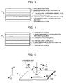
- Fig. 4 is a schematic view of a tunnel junction device according to an embodiment of the present invention.
- reference numeral 11 denotes a lower metal electrode
- reference numeral 12 denotes a ferromagnetic metal material La 0.6 Sr 0.4 MnO 3 as a lower ferromagnetic electroconductive electrode formed on the lower metal electrode
- reference numeral 13 denotes a tunneling film (insulating film) including two unit layers of single unit layer of LaMnO 3 as a first insulating layer 13A, five unit layers of SrTiO 3 as a second insulating layer 13B, and a two unit layers of LaMnO 3 as a third insulating layer 13C
- reference numeral 14 denotes a ferromagnetic metal film material La 0.6 Sr 0.4 MnO 3 as an upper ferromagnetic electroconductive electrode formed on the third insulating layer 13C
- reference numeral 15 denotes an upper metal electrode.
- the tunneling film as a nonmagnetic film of three-layer structure of LaMnO 3 /SrTiO 3 /LaMnO 3 is arranged between the ferromagnetic metal material La 0.6 Sr 0.4 MnO 3 12 and the ferromagnetic metal film material La 0.6 Sr 0.4 MnO 3 14.
- the tunneling film comprises two unit layers of LaMnO 3 13A arranged on the ferromagnetic metal material La 0.6 Sr 0.4 MnO 3 12; five unit layers of SrTiO 3 13B; and two unit layers of LaMnO 3 13C arranged between the SrTiO 3 13B and the ferromagnetic metal film material La 0.6 Sr 0.4 MnO 3 14.
- tunneling film 13, the ferromagnetic metal layers 12 and 14 are laminated by a laser abrasion process.
- the film formation herein is carried out under the conditions at 850°C to 900°C and 0.1 to 1 mTorr.
- One unit layer of the SrTiO 3 13B has a thickness of 3.905 angstroms
- one unit layer of the LaMnO 3 13C has a thickness of 3.960 angstroms.
- the number of layers constituting these films was determined by reflective high-energy electron diffraction (RHEED) observation.
- Measurement example of the deflection angle of the second harmonic (SHG) is shown below.
- the measurement is performed under the condition of reflection intensity of the second harmonic (SHG) being 3.1 eV at an incident energy of 1.55 eV, an incident angle of 26°, and a sample temperature of 50 K to 350 K.
- the SHG light is separated from the exciting light using an optical filter and a spectrometer and is measured using a photomultiplier and a boxcar integrator.
- Fig. 5 is a diagram illustrating the principle of an observation method of spin state at the interface using the second harmonic [MSHG (magnetic second harmonic generation) method].
- the interface under test comprises a nonmagnetic transparent film 101 and a ferromagnetic film 102.
- the nonmagnetic transparent film comprises SrTiO 3 as a comparative example of conventional material and SrTiO 3 /LaMnO 3 as an example of the present invention.
- the ferromagnetic film comprises La 0.6 Sr 0.4 MnO 3 both in the comparative example and the example of the present invention.
- the polarizability Pz occurs due to the presence of the interface, and the magnetization Mx in the x-axis direction induces ⁇ (2).
- the rotation angle of the polarization plane is proportional to the magnitude of the resulting interface magnetization.
- the rotation of the polarization plane of the second harmonic from the magnetic interface was theoretically predicted by Pustogowa et al. in an Fe magnetic metal thin film (Non-patent Document 4) and was observed by Rasing et al. in an Fe/Cr film formed by sputtered film (Non-patent Document 5).
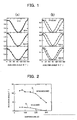
- Fig. 1(a) shows the degree of deflection of SHG light at B of +500 gauss and B of -500 gauss in a tunneling film using SrTiO 3 .
- SrTiO 3 has been conventionally used in CMR devices.
- Fig. 1(b) shows the degree of deflection of SHG light in a SrTiO 3 /LaMnO 3 tunneling film in the tunnel junction device of the present invention.
- Fig. 2 shows the degree of deflection of the SHG light within the range of 50 K to 350 K.
- the SHG light disappears when the tunneling film comprises SrTiO 3 (the graph a in Fig. 2), while the SHG light remains 40 percent of that at a low temperature of 50 K when the tunneling film is according to the present invention (the graph b in Fig. 2).
- a CMR device having a MR ratio of 40 percent of that at a low temperature e.g., 4.2 K
- a MR ratio of 720% at room temperature can be achieved, since a MR ratio of 1800% is achieved at 4.2 K, and 40 percent of 1800%, i.e., 720% can be achieved at room temperature.
- the novel CMR devices according to the present invention enable to provide high-performance magnetic sensors that operate at room temperature and have a MR ratio of 700 or more. This can provide immense magnetic memory devices of 100 gigabits up to the order of terabits and provide immense memories suitable for bearing information communications handling immense information in future.
- the novel CMR devices according to the present invention can be applied not only to magnetic sensors but also to magnetic memory devices which are now rapidly being developed. They can be possibly applied to oxide films for capacities of DRAM devices, since the tunneling current passing through such oxide film can be dramatically reduced by holding the directions of spins of materials for the ferromagnetic electroconductive electrodes in antiparallel state.
- the resulting article can be applied as open/close sensors such as those for mobile phones, since the CMR devices can detect a magnetic field in a microdomain.
- the present invention can be possibly applied not only to magnetic memories but also to elementary elements in broad information networks.
- the tunnel junction devices of the present invention are suitable for high-performance magnetic sensors that have a MR ratio of 700 or more and can operate at room temperature.
Landscapes
- Engineering & Computer Science (AREA)
- Chemical & Material Sciences (AREA)
- Physics & Mathematics (AREA)
- Crystallography & Structural Chemistry (AREA)
- Nanotechnology (AREA)
- Condensed Matter Physics & Semiconductors (AREA)
- General Physics & Mathematics (AREA)
- Manufacturing & Machinery (AREA)
- Power Engineering (AREA)
- Hall/Mr Elements (AREA)
- Mram Or Spin Memory Techniques (AREA)
- Thin Magnetic Films (AREA)
Applications Claiming Priority (2)
| Application Number | Priority Date | Filing Date | Title |
|---|---|---|---|
| JP2003302614A JP4133687B2 (ja) | 2003-08-27 | 2003-08-27 | トンネルジャンクション素子 |
| PCT/JP2004/008173 WO2005024968A1 (ja) | 2003-08-27 | 2004-06-04 | トンネルジャンクション素子 |
Publications (3)
| Publication Number | Publication Date |
|---|---|
| EP1659645A1 true EP1659645A1 (de) | 2006-05-24 |
| EP1659645A4 EP1659645A4 (de) | 2009-11-18 |
| EP1659645B1 EP1659645B1 (de) | 2010-11-03 |
Family
ID=34269181
Family Applications (1)
| Application Number | Title | Priority Date | Filing Date |
|---|---|---|---|
| EP04745776A Expired - Lifetime EP1659645B1 (de) | 2003-08-27 | 2004-06-04 | Tunnelübergangselement |
Country Status (6)
| Country | Link |
|---|---|
| US (1) | US7633723B2 (de) |
| EP (1) | EP1659645B1 (de) |
| JP (1) | JP4133687B2 (de) |
| KR (1) | KR100795747B1 (de) |
| DE (1) | DE602004029903D1 (de) |
| WO (1) | WO2005024968A1 (de) |
Cited By (1)
| Publication number | Priority date | Publication date | Assignee | Title |
|---|---|---|---|---|
| US11201189B2 (en) * | 2016-09-14 | 2021-12-14 | Toshiba Memory Corporation | Semiconductor device having rare earth oxide layer and method of manufacturing the same |
Families Citing this family (6)
| Publication number | Priority date | Publication date | Assignee | Title |
|---|---|---|---|---|
| DE112006000612T5 (de) * | 2005-03-23 | 2008-02-14 | National Institute Of Advanced Industrial Science And Technology | Nichtflüchtiges Speicherelement |
| JP4834834B2 (ja) * | 2006-05-08 | 2011-12-14 | 国立大学法人東北大学 | トンネル磁気抵抗素子、不揮発性磁気メモリ、発光素子および3端子素子 |
| US8829901B2 (en) * | 2011-11-04 | 2014-09-09 | Honeywell International Inc. | Method of using a magnetoresistive sensor in second harmonic detection mode for sensing weak magnetic fields |
| US9852835B2 (en) | 2014-07-17 | 2017-12-26 | University of Pittsburgh—of the Commonwealth System of Higher Education | Oxide interface displaying electronically controllable ferromagnetism |
| JP7086664B2 (ja) * | 2018-03-20 | 2022-06-20 | キオクシア株式会社 | 磁気装置 |
| GB202018825D0 (en) * | 2020-11-30 | 2021-01-13 | Univ Liverpool | Composition and method |
Family Cites Families (4)
| Publication number | Priority date | Publication date | Assignee | Title |
|---|---|---|---|---|
| US6110751A (en) * | 1997-01-10 | 2000-08-29 | Fujitsu Limited | Tunnel junction structure and its manufacture and magnetic sensor |
| JP2001320108A (ja) * | 2000-05-02 | 2001-11-16 | Canon Inc | 磁気抵抗素子、磁気メモリ及び磁気センサー |
| JP2002314164A (ja) * | 2001-02-06 | 2002-10-25 | Sony Corp | 磁気トンネル素子及びその製造方法、薄膜磁気ヘッド、磁気メモリ、並びに磁気センサ |
| JP3815601B2 (ja) | 2001-09-14 | 2006-08-30 | 独立行政法人産業技術総合研究所 | トンネル磁気抵抗素子および磁気ランダムアクセスメモリ |
-
2003
- 2003-08-27 JP JP2003302614A patent/JP4133687B2/ja not_active Expired - Lifetime
-
2004
- 2004-06-04 US US10/569,089 patent/US7633723B2/en not_active Expired - Fee Related
- 2004-06-04 KR KR1020067003839A patent/KR100795747B1/ko not_active Expired - Fee Related
- 2004-06-04 DE DE602004029903T patent/DE602004029903D1/de not_active Expired - Lifetime
- 2004-06-04 WO PCT/JP2004/008173 patent/WO2005024968A1/ja not_active Ceased
- 2004-06-04 EP EP04745776A patent/EP1659645B1/de not_active Expired - Lifetime
Cited By (1)
| Publication number | Priority date | Publication date | Assignee | Title |
|---|---|---|---|---|
| US11201189B2 (en) * | 2016-09-14 | 2021-12-14 | Toshiba Memory Corporation | Semiconductor device having rare earth oxide layer and method of manufacturing the same |
Also Published As
| Publication number | Publication date |
|---|---|
| KR20060069469A (ko) | 2006-06-21 |
| KR100795747B1 (ko) | 2008-01-17 |
| JP4133687B2 (ja) | 2008-08-13 |
| JP2005072436A (ja) | 2005-03-17 |
| DE602004029903D1 (de) | 2010-12-16 |
| EP1659645B1 (de) | 2010-11-03 |
| US20070058302A1 (en) | 2007-03-15 |
| EP1659645A4 (de) | 2009-11-18 |
| WO2005024968A1 (ja) | 2005-03-17 |
| US7633723B2 (en) | 2009-12-15 |
Similar Documents
| Publication | Publication Date | Title |
|---|---|---|
| JP5191652B2 (ja) | 感知向上層(senseenhancinglayer)を含む磁気感知デバイス | |
| US6631055B2 (en) | Tunnel valve flux guide structure formed by oxidation of pinned layer | |
| US7116532B2 (en) | Stability-enhancing underlayer for exchange-coupled magnetic structures, magnetoresistive sensors, and magnetic disk drive systems | |
| US20090322319A1 (en) | Magnetoresistive sensor with tunnel barrier and method | |
| JP2004186274A (ja) | スピン注入素子及びスピン注入素子を用いた磁気装置 | |
| CN105469809A (zh) | 隧道磁阻器件和隧道磁阻读磁头 | |
| WO2004059745A1 (ja) | 磁性スイッチ素子とそれを用いた磁気メモリ | |
| JP4061590B2 (ja) | 磁性薄膜及びそれを用いた磁気抵抗効果素子並びに磁気デバイス | |
| US7633723B2 (en) | Tunnel junction device having oxide ferromagnetic electroconductive electrodes and three-layer structure tunneling film | |
| JP3344712B2 (ja) | 磁気デバイスのピン止め層 | |
| JP5062832B2 (ja) | 磁気抵抗効果素子の製造方法 | |
| JP2001076479A (ja) | 磁気メモリ素子 | |
| US8091209B1 (en) | Magnetic sensing device including a sense enhancing layer | |
| JP2003318462A (ja) | 磁気抵抗効果素子とこれを用いた磁気ヘッドおよび磁気メモリ | |
| US7485937B2 (en) | Tunnel junction device | |
| EP3761050A1 (de) | Magnetfeldsensor zur messung eines zweidimensionalen externen magnetfeldes mit einem niedrigen anisotropiefeld | |
| JP3673661B2 (ja) | 磁気メモリ素子 | |
| JP2000299517A (ja) | 磁気抵抗素子及び磁気メモリ素子 | |
| JP2000306375A (ja) | 磁気抵抗素子及び磁気メモリ素子 | |
| JP2001345496A (ja) | 磁気素子 |
Legal Events
| Date | Code | Title | Description |
|---|---|---|---|
| PUAI | Public reference made under article 153(3) epc to a published international application that has entered the european phase |
Free format text: ORIGINAL CODE: 0009012 |
|
| 17P | Request for examination filed |
Effective date: 20060227 |
|
| AK | Designated contracting states |
Kind code of ref document: A1 Designated state(s): DE FR GB NL |
|
| RIN1 | Information on inventor provided before grant (corrected) |
Inventor name: KANEKO, YOSHIO Inventor name: KAWASAKI, M.,NAT. INST. OF ADVANCED IND. SCE. AND Inventor name: OGAWA, YOSHIHIRO Inventor name: YAMADA, H.,NAT. INST. OF ADVANCED IND. SCE. AND Inventor name: TOKURA, Y.,NAT. INST. OF ADVANCED IND. SCE. AND |
|
| DAX | Request for extension of the european patent (deleted) | ||
| RBV | Designated contracting states (corrected) |
Designated state(s): DE FR GB NL |
|
| A4 | Supplementary search report drawn up and despatched |
Effective date: 20091021 |
|
| 17Q | First examination report despatched |
Effective date: 20091215 |
|
| GRAP | Despatch of communication of intention to grant a patent |
Free format text: ORIGINAL CODE: EPIDOSNIGR1 |
|
| RIC1 | Information provided on ipc code assigned before grant |
Ipc: G01R 33/09 20060101ALI20100517BHEP Ipc: H01L 43/08 20060101AFI20100517BHEP Ipc: G11B 5/39 20060101ALI20100517BHEP Ipc: H01F 10/32 20060101ALI20100517BHEP |
|
| RIN1 | Information on inventor provided before grant (corrected) |
Inventor name: KANEKO, YOSHIO Inventor name: OGAWA, YOSHIHIRO Inventor name: KAWASAKI, MASASHI Inventor name: TOKURA, YOSHINORI Inventor name: YAMADA, HIROYUKI |
|
| GRAS | Grant fee paid |
Free format text: ORIGINAL CODE: EPIDOSNIGR3 |
|
| GRAA | (expected) grant |
Free format text: ORIGINAL CODE: 0009210 |
|
| AK | Designated contracting states |
Kind code of ref document: B1 Designated state(s): DE FR GB NL |
|
| REG | Reference to a national code |
Ref country code: GB Ref legal event code: FG4D |
|
| REF | Corresponds to: |
Ref document number: 602004029903 Country of ref document: DE Date of ref document: 20101216 Kind code of ref document: P |
|
| REG | Reference to a national code |
Ref country code: NL Ref legal event code: T3 |
|
| PLBE | No opposition filed within time limit |
Free format text: ORIGINAL CODE: 0009261 |
|
| STAA | Information on the status of an ep patent application or granted ep patent |
Free format text: STATUS: NO OPPOSITION FILED WITHIN TIME LIMIT |
|
| 26N | No opposition filed |
Effective date: 20110804 |
|
| REG | Reference to a national code |
Ref country code: DE Ref legal event code: R097 Ref document number: 602004029903 Country of ref document: DE Effective date: 20110804 |
|
| REG | Reference to a national code |
Ref country code: NL Ref legal event code: V1 Effective date: 20120101 |
|
| GBPC | Gb: european patent ceased through non-payment of renewal fee |
Effective date: 20110604 |
|
| REG | Reference to a national code |
Ref country code: FR Ref legal event code: ST Effective date: 20120229 |
|
| REG | Reference to a national code |
Ref country code: DE Ref legal event code: R119 Ref document number: 602004029903 Country of ref document: DE Effective date: 20120103 |
|
| PG25 | Lapsed in a contracting state [announced via postgrant information from national office to epo] |
Ref country code: DE Free format text: LAPSE BECAUSE OF NON-PAYMENT OF DUE FEES Effective date: 20120103 Ref country code: FR Free format text: LAPSE BECAUSE OF NON-PAYMENT OF DUE FEES Effective date: 20110630 |
|
| PG25 | Lapsed in a contracting state [announced via postgrant information from national office to epo] |
Ref country code: NL Free format text: LAPSE BECAUSE OF NON-PAYMENT OF DUE FEES Effective date: 20120101 |
|
| PG25 | Lapsed in a contracting state [announced via postgrant information from national office to epo] |
Ref country code: GB Free format text: LAPSE BECAUSE OF NON-PAYMENT OF DUE FEES Effective date: 20110604 |