EP1658968A2 - Verfahren zum eingeschränkten Sintern einer pseudo-symetrisch angeordneten Verbundkeramik bei tiefer Temperatur - Google Patents
Verfahren zum eingeschränkten Sintern einer pseudo-symetrisch angeordneten Verbundkeramik bei tiefer Temperatur Download PDFInfo
- Publication number
- EP1658968A2 EP1658968A2 EP05024389A EP05024389A EP1658968A2 EP 1658968 A2 EP1658968 A2 EP 1658968A2 EP 05024389 A EP05024389 A EP 05024389A EP 05024389 A EP05024389 A EP 05024389A EP 1658968 A2 EP1658968 A2 EP 1658968A2
- Authority
- EP
- European Patent Office
- Prior art keywords
- tape
- constraining
- glass
- primary
- self
- Prior art date
- Legal status (The legal status is an assumption and is not a legal conclusion. Google has not performed a legal analysis and makes no representation as to the accuracy of the status listed.)
- Granted
Links
Images



Classifications
-
- B—PERFORMING OPERATIONS; TRANSPORTING
- B32—LAYERED PRODUCTS
- B32B—LAYERED PRODUCTS, i.e. PRODUCTS BUILT-UP OF STRATA OF FLAT OR NON-FLAT, e.g. CELLULAR OR HONEYCOMB, FORM
- B32B18/00—Layered products essentially comprising ceramics, e.g. refractory products
-
- H—ELECTRICITY
- H05—ELECTRIC TECHNIQUES NOT OTHERWISE PROVIDED FOR
- H05K—PRINTED CIRCUITS; CASINGS OR CONSTRUCTIONAL DETAILS OF ELECTRIC APPARATUS; MANUFACTURE OF ASSEMBLAGES OF ELECTRICAL COMPONENTS
- H05K3/00—Apparatus or processes for manufacturing printed circuits
- H05K3/46—Manufacturing multilayer circuits
-
- C—CHEMISTRY; METALLURGY
- C03—GLASS; MINERAL OR SLAG WOOL
- C03C—CHEMICAL COMPOSITION OF GLASSES, GLAZES OR VITREOUS ENAMELS; SURFACE TREATMENT OF GLASS; SURFACE TREATMENT OF FIBRES OR FILAMENTS MADE FROM GLASS, MINERALS OR SLAGS; JOINING GLASS TO GLASS OR OTHER MATERIALS
- C03C14/00—Glass compositions containing a non-glass component, e.g. compositions containing fibres, filaments, whiskers, platelets, or the like, dispersed in a glass matrix
- C03C14/004—Glass compositions containing a non-glass component, e.g. compositions containing fibres, filaments, whiskers, platelets, or the like, dispersed in a glass matrix the non-glass component being in the form of particles or flakes
-
- C—CHEMISTRY; METALLURGY
- C04—CEMENTS; CONCRETE; ARTIFICIAL STONE; CERAMICS; REFRACTORIES
- C04B—LIME, MAGNESIA; SLAG; CEMENTS; COMPOSITIONS THEREOF, e.g. MORTARS, CONCRETE OR LIKE BUILDING MATERIALS; ARTIFICIAL STONE; CERAMICS; REFRACTORIES; TREATMENT OF NATURAL STONE
- C04B35/00—Shaped ceramic products characterised by their composition; Ceramics compositions; Processing powders of inorganic compounds preparatory to the manufacturing of ceramic products
- C04B35/622—Forming processes; Processing powders of inorganic compounds preparatory to the manufacturing of ceramic products
-
- H—ELECTRICITY
- H05—ELECTRIC TECHNIQUES NOT OTHERWISE PROVIDED FOR
- H05K—PRINTED CIRCUITS; CASINGS OR CONSTRUCTIONAL DETAILS OF ELECTRIC APPARATUS; MANUFACTURE OF ASSEMBLAGES OF ELECTRICAL COMPONENTS
- H05K3/00—Apparatus or processes for manufacturing printed circuits
- H05K3/46—Manufacturing multilayer circuits
- H05K3/4611—Manufacturing multilayer circuits by laminating two or more circuit boards
- H05K3/4626—Manufacturing multilayer circuits by laminating two or more circuit boards characterised by the insulating layers or materials
- H05K3/4629—Manufacturing multilayer circuits by laminating two or more circuit boards characterised by the insulating layers or materials laminating inorganic sheets comprising printed circuits, e.g. green ceramic sheets
-
- H—ELECTRICITY
- H05—ELECTRIC TECHNIQUES NOT OTHERWISE PROVIDED FOR
- H05K—PRINTED CIRCUITS; CASINGS OR CONSTRUCTIONAL DETAILS OF ELECTRIC APPARATUS; MANUFACTURE OF ASSEMBLAGES OF ELECTRICAL COMPONENTS
- H05K3/00—Apparatus or processes for manufacturing printed circuits
- H05K3/46—Manufacturing multilayer circuits
- H05K3/4688—Composite multilayer circuits, i.e. comprising insulating layers having different properties
-
- H—ELECTRICITY
- H10—SEMICONDUCTOR DEVICES; ELECTRIC SOLID-STATE DEVICES NOT OTHERWISE PROVIDED FOR
- H10W—GENERIC PACKAGES, INTERCONNECTIONS, CONNECTORS OR OTHER CONSTRUCTIONAL DETAILS OF DEVICES COVERED BY CLASS H10
- H10W70/00—Package substrates; Interposers; Redistribution layers [RDL]
- H10W70/01—Manufacture or treatment
- H10W70/05—Manufacture or treatment of insulating or insulated package substrates, or of interposers, or of redistribution layers
-
- H—ELECTRICITY
- H10—SEMICONDUCTOR DEVICES; ELECTRIC SOLID-STATE DEVICES NOT OTHERWISE PROVIDED FOR
- H10W—GENERIC PACKAGES, INTERCONNECTIONS, CONNECTORS OR OTHER CONSTRUCTIONAL DETAILS OF DEVICES COVERED BY CLASS H10
- H10W70/00—Package substrates; Interposers; Redistribution layers [RDL]
- H10W70/60—Insulating or insulated package substrates; Interposers; Redistribution layers
- H10W70/67—Insulating or insulated package substrates; Interposers; Redistribution layers characterised by their insulating layers or insulating parts
- H10W70/69—Insulating materials thereof
-
- H—ELECTRICITY
- H10—SEMICONDUCTOR DEVICES; ELECTRIC SOLID-STATE DEVICES NOT OTHERWISE PROVIDED FOR
- H10W—GENERIC PACKAGES, INTERCONNECTIONS, CONNECTORS OR OTHER CONSTRUCTIONAL DETAILS OF DEVICES COVERED BY CLASS H10
- H10W70/00—Package substrates; Interposers; Redistribution layers [RDL]
- H10W70/60—Insulating or insulated package substrates; Interposers; Redistribution layers
- H10W70/67—Insulating or insulated package substrates; Interposers; Redistribution layers characterised by their insulating layers or insulating parts
- H10W70/69—Insulating materials thereof
- H10W70/692—Ceramics or glasses
-
- H—ELECTRICITY
- H10—SEMICONDUCTOR DEVICES; ELECTRIC SOLID-STATE DEVICES NOT OTHERWISE PROVIDED FOR
- H10W—GENERIC PACKAGES, INTERCONNECTIONS, CONNECTORS OR OTHER CONSTRUCTIONAL DETAILS OF DEVICES COVERED BY CLASS H10
- H10W99/00—Subject matter not provided for in other groups of this subclass
-
- C—CHEMISTRY; METALLURGY
- C03—GLASS; MINERAL OR SLAG WOOL
- C03C—CHEMICAL COMPOSITION OF GLASSES, GLAZES OR VITREOUS ENAMELS; SURFACE TREATMENT OF GLASS; SURFACE TREATMENT OF FIBRES OR FILAMENTS MADE FROM GLASS, MINERALS OR SLAGS; JOINING GLASS TO GLASS OR OTHER MATERIALS
- C03C2214/00—Nature of the non-vitreous component
- C03C2214/04—Particles; Flakes
-
- C—CHEMISTRY; METALLURGY
- C03—GLASS; MINERAL OR SLAG WOOL
- C03C—CHEMICAL COMPOSITION OF GLASSES, GLAZES OR VITREOUS ENAMELS; SURFACE TREATMENT OF GLASS; SURFACE TREATMENT OF FIBRES OR FILAMENTS MADE FROM GLASS, MINERALS OR SLAGS; JOINING GLASS TO GLASS OR OTHER MATERIALS
- C03C2214/00—Nature of the non-vitreous component
- C03C2214/30—Methods of making the composites
-
- C—CHEMISTRY; METALLURGY
- C04—CEMENTS; CONCRETE; ARTIFICIAL STONE; CERAMICS; REFRACTORIES
- C04B—LIME, MAGNESIA; SLAG; CEMENTS; COMPOSITIONS THEREOF, e.g. MORTARS, CONCRETE OR LIKE BUILDING MATERIALS; ARTIFICIAL STONE; CERAMICS; REFRACTORIES; TREATMENT OF NATURAL STONE
- C04B2235/00—Aspects relating to ceramic starting mixtures or sintered ceramic products
- C04B2235/60—Aspects relating to the preparation, properties or mechanical treatment of green bodies or pre-forms
- C04B2235/602—Making the green bodies or pre-forms by moulding
- C04B2235/6025—Tape casting, e.g. with a doctor blade
-
- C—CHEMISTRY; METALLURGY
- C04—CEMENTS; CONCRETE; ARTIFICIAL STONE; CERAMICS; REFRACTORIES
- C04B—LIME, MAGNESIA; SLAG; CEMENTS; COMPOSITIONS THEREOF, e.g. MORTARS, CONCRETE OR LIKE BUILDING MATERIALS; ARTIFICIAL STONE; CERAMICS; REFRACTORIES; TREATMENT OF NATURAL STONE
- C04B2235/00—Aspects relating to ceramic starting mixtures or sintered ceramic products
- C04B2235/65—Aspects relating to heat treatments of ceramic bodies such as green ceramics or pre-sintered ceramics, e.g. burning, sintering or melting processes
- C04B2235/656—Aspects relating to heat treatments of ceramic bodies such as green ceramics or pre-sintered ceramics, e.g. burning, sintering or melting processes characterised by specific heating conditions during heat treatment
- C04B2235/6562—Heating rate
-
- C—CHEMISTRY; METALLURGY
- C04—CEMENTS; CONCRETE; ARTIFICIAL STONE; CERAMICS; REFRACTORIES
- C04B—LIME, MAGNESIA; SLAG; CEMENTS; COMPOSITIONS THEREOF, e.g. MORTARS, CONCRETE OR LIKE BUILDING MATERIALS; ARTIFICIAL STONE; CERAMICS; REFRACTORIES; TREATMENT OF NATURAL STONE
- C04B2235/00—Aspects relating to ceramic starting mixtures or sintered ceramic products
- C04B2235/65—Aspects relating to heat treatments of ceramic bodies such as green ceramics or pre-sintered ceramics, e.g. burning, sintering or melting processes
- C04B2235/656—Aspects relating to heat treatments of ceramic bodies such as green ceramics or pre-sintered ceramics, e.g. burning, sintering or melting processes characterised by specific heating conditions during heat treatment
- C04B2235/6565—Cooling rate
-
- C—CHEMISTRY; METALLURGY
- C04—CEMENTS; CONCRETE; ARTIFICIAL STONE; CERAMICS; REFRACTORIES
- C04B—LIME, MAGNESIA; SLAG; CEMENTS; COMPOSITIONS THEREOF, e.g. MORTARS, CONCRETE OR LIKE BUILDING MATERIALS; ARTIFICIAL STONE; CERAMICS; REFRACTORIES; TREATMENT OF NATURAL STONE
- C04B2237/00—Aspects relating to ceramic laminates or to joining of ceramic articles with other articles by heating
- C04B2237/30—Composition of layers of ceramic laminates or of ceramic or metallic articles to be joined by heating, e.g. Si substrates
- C04B2237/32—Ceramic
- C04B2237/34—Oxidic
- C04B2237/341—Silica or silicates
-
- C—CHEMISTRY; METALLURGY
- C04—CEMENTS; CONCRETE; ARTIFICIAL STONE; CERAMICS; REFRACTORIES
- C04B—LIME, MAGNESIA; SLAG; CEMENTS; COMPOSITIONS THEREOF, e.g. MORTARS, CONCRETE OR LIKE BUILDING MATERIALS; ARTIFICIAL STONE; CERAMICS; REFRACTORIES; TREATMENT OF NATURAL STONE
- C04B2237/00—Aspects relating to ceramic laminates or to joining of ceramic articles with other articles by heating
- C04B2237/50—Processing aspects relating to ceramic laminates or to the joining of ceramic articles with other articles by heating
- C04B2237/56—Using constraining layers before or during sintering
- C04B2237/564—Using constraining layers before or during sintering made of glass
-
- H—ELECTRICITY
- H05—ELECTRIC TECHNIQUES NOT OTHERWISE PROVIDED FOR
- H05K—PRINTED CIRCUITS; CASINGS OR CONSTRUCTIONAL DETAILS OF ELECTRIC APPARATUS; MANUFACTURE OF ASSEMBLAGES OF ELECTRICAL COMPONENTS
- H05K1/00—Printed circuits
- H05K1/02—Details
- H05K1/03—Use of materials for the substrate
- H05K1/0306—Inorganic insulating substrates, e.g. ceramic, glass
-
- H—ELECTRICITY
- H05—ELECTRIC TECHNIQUES NOT OTHERWISE PROVIDED FOR
- H05K—PRINTED CIRCUITS; CASINGS OR CONSTRUCTIONAL DETAILS OF ELECTRIC APPARATUS; MANUFACTURE OF ASSEMBLAGES OF ELECTRICAL COMPONENTS
- H05K1/00—Printed circuits
- H05K1/16—Printed circuits incorporating printed electric components, e.g. printed resistors, capacitors or inductors
- H05K1/162—Printed circuits incorporating printed electric components, e.g. printed resistors, capacitors or inductors incorporating printed capacitors
-
- Y—GENERAL TAGGING OF NEW TECHNOLOGICAL DEVELOPMENTS; GENERAL TAGGING OF CROSS-SECTIONAL TECHNOLOGIES SPANNING OVER SEVERAL SECTIONS OF THE IPC; TECHNICAL SUBJECTS COVERED BY FORMER USPC CROSS-REFERENCE ART COLLECTIONS [XRACs] AND DIGESTS
- Y10—TECHNICAL SUBJECTS COVERED BY FORMER USPC
- Y10T—TECHNICAL SUBJECTS COVERED BY FORMER US CLASSIFICATION
- Y10T428/00—Stock material or miscellaneous articles
- Y10T428/24—Structurally defined web or sheet [e.g., overall dimension, etc.]
- Y10T428/24802—Discontinuous or differential coating, impregnation or bond [e.g., artwork, printing, retouched photograph, etc.]
- Y10T428/24926—Discontinuous or differential coating, impregnation or bond [e.g., artwork, printing, retouched photograph, etc.] including ceramic, glass, porcelain or quartz layer
Definitions
- This invention relates to a flat, distortion-free, zero-shrink, low-temperature co-fired ceramic (LTCC) bodies, composites, modules or packages from precursor green (unfired) laminates of three or more different dielectric tape chemistries that are configured in an uniquely or pseudo-symmetrical arrangement in the z-axis of the laminate.
- LTCC low-temperature co-fired ceramic
- An interconnect circuit board or package is the physical realization of electronic circuits or subsystems from a number of extremely small circuit elements electrically and mechanically interconnected. It is frequently desirable to combine these diverse type electronic components in an arrangement so that they can be physically isolated and mounted adjacent to one another in a single compact package and electrically connected to each other and/or to common connections extending from the package.
- circuits generally require that the circuit be constructed of several levels of conductors separated by corresponding insulating dielectric tape layers.
- the conductor layers are interconnected through the dielectric layers that separate them by electrically conductive pathways, called via fills.
- tape layer or dielectric layer implies the presence of metallizations both surface conductor and interconnecting via fills which are cofired with the ceramic tape.
- laminate or composite implies a collection of metallized tape layers that have been pressed together to form a single entity.
- the release tape acts to pin and restrain any possible shrinkage in x- and y-directions.
- the release tape itself does not sinter to any appreciable degree and is removed prior to any subsequent circuit manufacturing operation. Removal is achieved by one of a number of suitable procedures such as brushing, sand blasting or bead blasting.
- the use of the sacrificial constraining tape or release tape means that the user must purchase a tape material that does not reside in the final product.
- the top and bottom conductors cannot be co-processed with the laminate. These necessary steps may only be carried as part of a post-fired strategy after firing and removal of the release tape.
- U.S. patent application 60/385,697 the teachings of constrained sintering are extended to include the use of a non-fugitive, non-removable, non-sacrificial or non-release, internal self-constraining tape.
- the fired laminate comprises layers of a primary dielectric tape which define the bulk properties of the final ceramic body and one or more layers of a secondary or self-constraining tape.
- the purpose of the latter is to constrain the sintering of the primary tape so that the net shrinkage in the x, y direction is zero.
- This process is referred to as a self-constraining pressure-less assisted sintering process and the acronym SCPLAS is applied.
- FIGURE 1 which contains some generic dielectric tape arrangements, is used to illustrate the definition of z-axis symmetry as noted in U.S. Patent Application 60/385,697.
- SC self-constraining
- the criterion is that the distribution of the two tape materials (100, 101) is balanced in terms of thickness and position around the centerline (103) of the structure. The consequence of not preserving z-axis symmetry is a severely bowed or cambered circuit.
- dielectric layers with a higher dielectric constant (k) than the bulk dielectric material can produce localized enhanced capacitor capability when suitably terminated with a conductor material.
- This is commonly referred to as a buried passive structure and is a robust and cost-effective alternative to the use of standard, externally applied, surface mount components such as multilayer capacitors (MLC).
- MLC multilayer capacitors
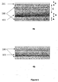
- FIGURE 3 shows some examples of some simple asymmetric arrangements. Actual designs would be more complex. Nonetheless, regardless of the complexity factor, the most intractable problem associated with such arrangements is that the structure will bow or camber to an unacceptable degree after co-firing. Moreover it will be cambered to a degree that will render it unusable for subsequent processing such as assembly by pick and place of passive and active surface components.
- the conventional definition of unacceptable camber or bowing is greater than an 0.003 inch deflection of the center point of a substrate per one inch of substrate diagonal length, e.g. a total of 0.025 inches for a 6" x 6" co-fired substrate. Different operations have different requirements but the above definition meets the majority of applications. The extent of this disadvantage increases with substrate size. It can pass almost unnoticed for substrates less than 2" x 2" but becomes very marked as the standard substrate dimension is increased to 6" x 6".
- the asymmetric structures as illustrated in FIGURE 3 cannot be co-fired flat by conventional processing techniques. They will tend to bow or camber in a concave manner i.e. the two edges of the laminate will be significantly higher than the center-point in the direction perpendicular to the plane of maximum asymmetry.
- an internal constraining layer (101) is formulated to provide a self-constraining function and an embedded capacitor function within a LTCC assembly.
- the properties of the processed internal constraining layer provide a rigid physical form restraining x and y shrinkage of primary tapes (100) and impart functional properties to the final LTCC assembly.
- the internal constraining tape precedes the sintering of the primary tape layers.
- a layer of removable, non permanent release layer (201) is applied to the outside surface directly opposite the source of greatest asymmetry. This enables extremely asymmetric structures to be fired flat. After firing, the release layer is removed using conventional brushing or sand blasting methods.
- the current invention represents an innovative approach to produce a structure exhibiting an interactive suppression of x,y shrinkage without the use of a sacrificial dielectric release tape at one side of the laminate as specified in U.S. patent application 10/430,081.
- the present invention is a distortion-free and camber-free, asymmetrical, low-temperature co-fired ceramic structure consisting essentially of one or more layers of low k glass-containing internal self-constraining tape, one or more layers of high k glass-containing internal self-constraining tape, and at least one layer of glass-containing primary tape wherein the dielectric constant of the low k tape is less than 8, the dielectric constant of the high k tape is greater than 8 and wherein each self-constraining tape can independently provide a self-constraining pressure-less assisted sintering LTCC assembly with the primary tape and wherein the self-constraining tapes are arranged to preserve structural symmetry regarding the class of self-constraining tapes as an entity with respect to the primary tape wherein the internal constraining tapes and the primary tape are laminated to form a compositionally asymmetrical laminate and wherein the assembly is thermally processed producing a structure exhibiting an interactive suppression of x,y shrinkage.
- the current invention further extends the concept of making asymmetrical configured LTCC dielectric multilayer circuits to include at least two internal constraining tapes having the same or different k values, without the use of sacrificial release tape at one side of the multilayer laminate.
- each internal constraining tape (501 or 502) can independently provide a zero-shrink SCPLAS system with the primary tape (100), and
- the internal constraining tapes are arranged to preserve structural symmetry regarding the class of internal constraining tapes as an entity with respect to primary tape.
- the structure of the LTCC multilayer circuit of the present invention may be asymmetrical around the centerline, there is still a requirement that the internal constraining tapes be arranged to preserve structural symmetry regarding the class of internal constraining tapes as an entity with respect to the primary tape.
- the level of shrinkage associated with each piece independently should be the same (or about the same) to ensure a uniform shrinkage with regard to the structure as a whole.
- the preferred level of shrinkage for the structure as a whole is zero-shrinkage, although any uniform level may be achieved for the structure as a whole, as long as each independent piece about the centerline may achieve the same shrinkage level independently.
- the differences in the dielectric tape chemistry result from differences in the types and compositions of the glass(es) or the filler(s) used to formulate the tapes and reflect in their corresponding dielectric constant (k) at any given frequency.
- a standard k is between 7 and 9.
- the typical primary tape is generally at a k value between 7 and 9, although this k value is not a necessary requirement of the primary tape.
- a tape with a k value at or lower than 8 is considered a low k tape
- a tape with a k value greater than 8 is considered a high k tape. It is therefore apparent that the high k values can be multiples of tens, hundreds, or thousands as far as this invention is concerned.
- tapes having k values within 0-15% of one another are considered to have the same k.
- the multilayer circuit can be fired flat and provide zero-shrink without the use of a sacrificial release tape as described in the prior art noted above.
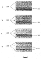
- FIGs 5a-5d illustrate various multilayer arrangements of internal constraining tapes and primary tape according to this invention. It is noted that the present invention can be applied but not limited to these examples.
- Internal constraining tapes 501 and 502 form the central core in 5a.
- Internal constraining tape 501 or 502 serves as the constraining layer in the upper or lower portion of structure in 5b.
- Either internal constraining tape 501 or 502 by itself can form the core as in 5c, which is the simplest configuration of this invention and represents a typical SCPLAS concept previously filed for patent.
- Figure 5d illustrates an expanded version of 5b to include flexibility in tape thickness and layer count variation.
- the internal constraining tape (501, 502) as utilized in the present invention contains glasses that flow, densify, and become rigid at temperatures significantly below 850°C, which is a standard process temperature. Because the constraining tape becomes part of the final LTCC body it significantly increases the performance requirements for the constraining tape material.
- the electrical properties (e.g., dielectric constant k) of the constraining tape may also be adjusted with a choice of materials that make up the tape. This makes possible the use of more than one chemical type of primary tape to locally control the dielectric and other electrical properties of a portion of a LTCC circuit.
- the primary tape (100) is generally the majority tape in a LTCC assembly and the resultant fired assembly derives its mechanical and electrical characteristics from it. In most situations the constraining tape has a minority presence in the structure. It can be used effectively to locally modify aspects of the dielectric and other electrical performance of the assembly, but its biggest influence is to control the physical structure by constraining its x,y shrinkage substantially to zero.
- the glass in the constraining tapes (low or high k, respectively for 501 or 502) attains its transition temperature (the temperature at which the glass initiates sintering, followed by flow and densification) earlier than the glass of the primary tape (low k) and it flows sufficiently to coat the surface particles of the adjacent layers of the primary tape. Since the crystallization temperature of the constraining tape glass is both close to and above its transition temperature, crystallization occurs very soon thereafter. This has the result of stiffening the glass and significantly raising its composite viscosity or elevating its re-melting temperature beyond the peak firing temperature of 825 to 875°C of the first co-firing and/or subsequent post-firing process.
- the constraining influence of the primary tape ensures that x,y shrinkage in the constraining tape is very small, if not zero. Subsequent increases in temperature cause the constraining tape to sinter fully and its glass to complete its crystallization. Since a suitable glass will, typically, develop in excess of 50 volume % crystalline phases, the constraining tape body becomes rigid when dominated by the volumetric accumulation of crystalline content of filler and in site formation of crystal from the glass. Then, when the transition temperature of the primary tape glass is achieved and flow occurs, it is kept physically in place by its previous interaction with the constraining tapes. Thus, the already-sintered constraining tape layers become the constraining force and the primary tape is constrained while sintering to shrink only in the z-direction.
- the two different internal constraining tapes, 501 and 502 are in direct contact.
- This type of structure requires sufficient interfacial bonding between the internal constraining tapes without significant inter-diffusion of glass from either or both tapes during the firing process:
- the primary tape (100) serves as the constraining force for both internal constraining tapes (501, 502) in the lower temperature range; and the sintered and crystalline, rigid SC layers serve as the constraining force for the primary tape in the higher temperature range.
- Such an innovation offers the advantages of facilitating cofireable top and bottom conductors, relieves the practical restrictions that externally-constrained sintered structures experience as the layer count is increased and the constraining influence of the external release tape is felt less and less. Furthermore, there is no need to remove the sacrificial constraining tape by mechanical and/or chemical means. This represents a saving of material and equipment expenditure and labor, and also possible environmental contamination.
- the use of the constraining tape allows the formation of exactly dimensioned, non-shrink cavities in a tape structure. Both blind and through cavities can be produced by this constrained sintering technique.
- the constraining tapes must be thermally processed to a rigid body prior to the primary tape to provide proper system x,y constraint.
- the glass-filler material in the constraining tapes should be designed to attain a lower composite viscosity to the primary tape, but at approximately 50-150°C lower in temperature and preferably in the range of 80-150°C.
- the above assessment was based on a belt furnace firing profile at an ascending rate of 6-8°C per minute between 450°C and - 850°C. Such a profile is commonly used to achieve high throughput in mass production of LTCC circuit substrates. However, a smaller temperature difference (e.g.
- ⁇ 50°C can also be effective if the firing profile in a multiple zone belt or box furnace provides a plateau to facilitate the full densification, and/or crystallization, and revivification of the constraining tapes. It should also provide sufficient compatibility between constraining and primary tapes during the densification to maintain the strength and bonding at the respective tape interfaces. This compatibility can be influenced by tape formulation, physical characteristics of the constituents and changes in thermal processing conditions. The electrical properties of the constraining tape materials must also meet performance requirements for high frequency circuit applications.
- the internal constraining tapes (501, 502) are further characterized as composed of a filler ceramic material such as Al 2 O 3 , TiO 2 , ZrO 2 , ZrSiO 4 , BaTiO 3 , etc., with a crystallizable or filler reactable glass composition so that its flow, densification and rigidification during firing proceed the remaining layers of primary tape.
- a constraining or primary tape normally may consist of a glass and filler, it may be designed by skilled artisans to utilize more than one glass or more than one filler.
- the physical act of restricting the x,y shrinkage of the constraining tapes by the primary tape during thermal processing is quite similar to the externally applied release layers of a conventional primary tape assembly.
- glasses that may be used in the primary or constraining tape are listed in Table 1.
- Preferred glass compositions found in the high k constraining tape comprise the following oxide constituents in the compositional range of: B 2 O 3 6-13, BaO 20-22, Li 2 O 0.5-1.5, P 2 O 5 3.5-4.5, TiO 2 25-33, Cs 2 O 1-6.5, Nd 2 O 3 29-32 in weight %.
- the more preferred composition of glass being: B 2 O 3 11.84, BaO 21.12,Li 2 O 1.31, P 2 O 5 4.14, TiO 2 25.44, Cs 2 O 6.16, Nd 2 O 3 29.99 in weight %.
- Another preferred glass comprises the following oxide constituents in the compositional range of: SiO 2 12-14, ZrO 2 3-6, B 2 O 3 20-27, BaO 12-15, MgO 33-36, Li 2 O 1-3, P 2 O 5 3-8, Cs 2 O 0-2 in weight %.
- the preferred composition of glass being: SiO 2 13.77, ZrO 2 4.70, B 2 O 3 26.10, BaO 14.05, MgO 35.09, Li 2 O 1.95, P 2 O 5 4.34 in weight %.
- composition 18 has been added as similar to the primary tape glass shown in composition 17. Additional high k glass compositions have been found to perform as suitable constraining tapes when incorporated into a standard tape formulation. These additional compositions are designated ID #19 and #20. These compositions are similar to the previously noted preferred compositions with the exception that Cs 2 O has been replaced by K 2 O with no loss or change of functional property.
- Example glasses for use in the low k constraining tapes comprise the following oxide constituents in the compositional range of: Glass #2 Table1 is an example of a glass that has a suitably low dielectric constant while serving suitably as a constraining glass in an LTCC tape structure.
- the dielectric constant of a tape composed of this glass (3.06g/cc) and 33.9 volume % alumina filler having a D50 PSD of 2.5 micron is about 8.
- Glasses 21 and 22 in the above table are examples of constraining tape glasses that are not suitable to achieve essentially zero x,y shrinkage when paired with a primary glass such as tape made from glass 15, 17 or 18.
- the TMA characteristics are somewhat higher to onset sintering than suitable constraining glasses such as glass #2, #6, #19 or #20. This prevents the complete attainment of zero X, Y shrinkage.
- the design of glass varies significantly from that in the high k constraining tape. It is well known that the choice of inorganic filler(s) in the constraining tape compositions also affect their resultant k; hence the tape compositions represent an overall property balance in order to provide zero-shrink, material compatibility, and desirable electrical performance such as k and loss tangent for high frequency applications.
- Preferred glasses for use in the primary tape comprise the following oxide constituents in the compositional range of: SiO 2 52-54, Al 2 O 3 12.5-14.5, B 2 O 3 8-9, CaO 16-18, MgO 0.5-5, Na 2 O 1.7-2.5, Li 2 O 0.2-0.3, SrO 0-4, K 2 O 1-2 in weight %.
- composition of glass being: SiO 2 53.50, Al 2 O 3 13.00, B 2 O 3 8.50, CaO 17.0, MgO 1.00 Na 2 O 2.25, Li 2 O 0.25, SrO 3.00, K 2 O 1.50 in weight %.
- the D 50 (median particle size) of frit is preferably in the range of, but not limited to, 0.1 to 5.0 microns and more preferably 0.3 to 3.0 microns.
- the constraining tapes must undergo simultaneous densification and crystallization, their averaged glass particle size and particle size distribution are most critical for the attainment of desirable microstructure within the temperature range above the organic burnout (pyrolysis) and the softening point of the glass in the primary tape,
- the glasses described herein are produced by conventional glass making techniques.
- the glasses were prepared in 500-1000 gram quantities. Typically, the ingredients are weighed then mixed in the desired proportions and heated in a bottom-loading furnace to form a melt in platinum alloy crucibles. As well known in the art, heating is conducted to a peak temperature (1450-1600°C) and for a time such that the melt becomes entirely liquid and homogeneous.
- the glass melts were quenched using a counter rotating stainless steel roller to form a 10-20 mil. thick platelet of glass.
- the resulting glass platelet was then milled to form a powder with its 50% volume distribution set between 1-5 microns.
- the glass powders were then formulated with filler and organic medium to cast tapes as detailed in the Examples section.
- the glass compositions shown in Table 1 represent a broad variety of glass chemistry (high amounts of glass former to low amounts of glass former).
- the glass former oxides are typically small size ions with high chemical coordination numbers such as SiO 2 , B 2 O 3 , and P 2 O 5 .
- the remaining oxides represented in the table are considered glass modifiers and intermediates.
- Ceramic filler such as Al 2 O 3 , ZrO 2 , TiO 2 , ZrSiO 4 , BaTiO 3 or mixtures thereof may be added to the castable composition used to form the tapes in an amount of 0-50 wt. % based on solids. Depending on the type of filler, different crystalline phases are expected to form after firing.
- the filler can control dielectric constant and loss over the frequency range. For example, the addition of BaTiO 3 can increase the dielectric constant significantly.
- Al 2 O 3 is the preferred ceramic filler since it reacts with the glass to form an Al-containing crystalline phase. Al 2 O 3 is very effective in providing high mechanical strength and inertness against detrimental chemical reactions. Another function of the ceramic filler is rheological control of the entire system during firing. The ceramic particles limit flow of the glass by acting as a physical barrier. They also inhibit sintering of the glass and thus facilitate better burnout of the organics. Other fillers, ⁇ -quartz, CaZrO 3 , mullite, cordierite, forsterite, zircon, zirconia, BaTiO 3 , CaTiO 3 , MgTiO 3 , SiO 2 , amorphous silica or mixtures thereof may be used to modify tape performance and characteristics. It is preferred that the filler has at least a bimodal particle size distribution with D50 of the larger size filler in the range of 1.5 and 3 microns and the D50 of the smaller size filler in the range of 0.3 and 0.8 microns.
- the amount of glass relative to the amount of ceramic material is important.
- a filler range of 20-40% by weight is considered desirable in that the sufficient densification is achieved. If the filler concentration exceeds 50% by wt., the fired structure is not sufficiently densified and is too porous. Within the desirable glass/filler ratio, it will be apparent that, during firing, the liquid glass phase will become saturated with filler material.
- the inorganic solids For the purpose of obtaining higher densification of the composition upon firing, it is important that the inorganic solids have small particle sizes. In particular, substantially all of the particles should not exceed 15 ⁇ m and preferably not exceed 10 ⁇ m. Subject to these maximum size limitations, it is preferred that at least 50% of the particles, both glass and ceramic filler, be greater than 1 ⁇ m and less than 6 ⁇ m.
- the organic medium in which the glass and ceramic inorganic solids are dispersed is comprised of a polymeric binder which is dissolved in a volatile organic solvent and, optionally, other dissolved materials such as plasticizers, release agents, dispersing agents, stripping agents, antifoaming agents, stabilizing agents and wetting agents.
- U.S. Patent No. 4,536,535 to Usala has disclosed an organic binder which is a mixture of compatible multipolymers of 0-100% wt. C 1-8 alkyl methacrylate, 100-0% wt. C 1-8 alkyl acrylate and 0-5% wt. ethylenically unsaturated carboxylic acid of amine. Because the above polymers can be used in minimum quantity with a maximum quantity of dielectric solids, they are preferably selected to produce the dielectric compositions of this invention. For this reason, the disclosure of the above-referred Usala application is incorporated by reference herein.
- the polymeric binder will also contain a small amount, relative to the binder polymer, of a plasticizer that serves to lower the glass transition temperature (Tg) of the binder polymer.
- a plasticizer that serves to lower the glass transition temperature (Tg) of the binder polymer.
- Tg glass transition temperature
- plasticizers which have been used in various binder systems are diethyl phthalate, dibutyl phthalate, dioctyl phthalate, butyl benzyl phthalate, alkyl phosphates, polyalkylene glycols, glycerol, poly(ethylene oxides), hydroxyethylated alkyl phenol, dialkyldithiophosphonate and poly(isobutylene).
- butyl benzyl phthalate is most frequently used in acrylic polymer systems because it can be used effectively in relatively small concentrations.
- the solvent component of the casting solution is chosen so as to obtain complete dissolution of the polymer and sufficiently high volatility to enable the solvent to be evaporated from the dispersion by the application of relatively low levels of heat at atmospheric pressure.
- the solvent must boil well below the boiling point or the decomposition temperature of any other additives contained in the organic medium. Thus, solvents having atmospheric boiling points below 150°C are used most frequently.
- Such solvents include acetone, xylene, methanol, ethanol, isopropanol, methyl ethyl ketone, ethyl acetate, 1,1,1-trichloroethane, tetrachloroethylene, amyl acetate, 2,2,4-triethyl pentanediol-1,3-monoisobutyrate, toluene, methylene chloride and fluorocarbons.
- Individual solvents mentioned above may not completely dissolve the binder polymers. Yet, when blended with other solvent(s), they function satisfactorily. This is well within the skill of those in the art.
- a particularly preferred solvent is ethyl acetate since it avoids the use of environmentally hazardous chlorocarbons.
- a plasticizer is used to prevent tape cracking and provide wider latitude of as-coated tape handling ability such as blanking, printing, and lamination.
- a preferred plasticizer is BENZOFLEX® 400 manufactured by Rohm and Haas Co., which is a polypropylene glycol dibenzoate.
- a green tape for use as a constraining tape or a primary tape is formed by casting a thin layer of a slurry dispersion of the glass, ceramic filler, polymeric binder and solvent(s) as described above onto a flexible substrate, heating the cast layer to remove the volatile solvent.
- the primary tape not exceed 20 mils in thickness and preferably 1 to 10 mils.
- the constraining tapes be 1 to 10 mils and preferably 1 to 3 mils in thickness.
- the tape is then blanked into sheets or collected in a roll form.
- the green tape is typically used as a dielectric or insulating material for multilayer electronic circuits. A sheet of green tape is blanked with registration holes in each corner to a size somewhat larger than the actual dimensions of the circuit.
- via holes are formed in the green tape. This is typically done by mechanical punching. However, a sharply focused laser can be used to volatilize and form via holes in the green tape. Typical via hole sizes range from 0.004" to 0.25".
- the interconnections between layers are formed by filling them via holes with a thick film conductive ink. This ink is usually applied by standard screen printing techniques.
- Each layer of circuitry is completed by screen printing conductor tracks.
- resistor inks or high dielectric constant inks can be printed on selected layer(s) to form resistive or capacitive circuit elements.
- specially formulated high dielectric constant green tapes similar to those used in the multilayer capacitor industry can be incorporated as part of the multilayer circuitry.
- the individual layers are collated and laminated.
- a confined uniaxial or isostatic pressing die is used to insure precise alignment between layers.
- the laminates are trimmed with a hot stage cutter. Firing is carried out in a standard thick film conveyor belt furnace or in a box furnace with a programmed heating cycle. This method will, also, allow top and/or bottom conductors to be cofired as part of the constrained sintered structure without the need for using a conventional release tape as the top and bottom layer, and the removal, and cleaning of the release tape after firing.
- firing means heating the assemblage in an oxidizing atmosphere such as air to a temperature, and for a time sufficient to volatilize (burn-out) all of the organic material in the layers of the assemblage to sinter any glass, metal or dielectric material in the layers and thus densify the entire laminate.
- a typical green tape layer may have printed thereon one or more resistor circuits and/or capacitors as well as conductive circuits.
- green tape sheets of various thickness were blanked with corner registration holes into sheets with x- and y-dimensions ranging from 3" x 3" to 8" x 8". These were then punched to form via holes and then metallized with suitable surface and via fill conductors using standard processing techniques which are well known to those skilled in the art.
- the parts were then fired by heating in an oxidizing atmosphere such as air to a temperature, and for a time sufficient to volatilize (burn-out) all of the organic material in the layers of the assemblage to sinter any glass, metal or dielectric material in the layers. In this way the entire laminate was densified.
- an oxidizing atmosphere such as air
- Tape compositions used in the examples were prepared by ball milling the fine inorganic powders and binders in a volatile solvent or solvent blend. To optimize the lamination, the ability to pattern circuits, the tape burnout properties and the fired microstructure development, the following volume % formulation of slip was found to provide advantages. The formulation of typical slip compositions is also shown in weight percentage, as a practical reference.
- the inorganic phase is assumed to have a specific density of 4.5 g/cc for glass and 4.0 g/cc for alumina and the organic vehicle is assumed to have a specific density of 1.1 g/cc.
- the weight % composition changes accordingly when using glass and oxides other than alumina as the specific density maybe different than those assumed in this example.
- the composition for the slip must include sufficient solvent to lower the viscosity to less than 10,000 centipoise; typical viscosity ranges are 1,000 to 4,000 centipoise.
- An example of a slip composition is provided in Table 2. Depending on the chosen slip viscosity, higher viscosity slip prolongs the dispersion stability for a longer period of time (normally several weeks). A stable dispersion of tape constituents is usually preserved in the as-coated tape.
- the glasses for the Examples found herein were all melted in Pt/Rh crucibles at 1450-1600°C for about 1 hour in an electrically heated furnace. Glasses were quenched by metal roller as a preliminary step and then subjected to particle size reduction by milling. The powders prepared for these tests were adjusted to a 1-5 micron mean size by milling prior to formulation as a slip. Since additional milling is utilized in the fabrication of slip, the final mean size is normally in the range of 1-3 microns.
- the influence of the total/constraining tape thickness is seen to relate in general to the x,y-shrinkage values, and the smaller the ratio, the smaller the x,y-shrinkage.
- a Primary #2 Tape (4.5 mils thick) is paired with two different constraining tape compositions (Constraining #1 and Constraining #2) having identical total/constraining tape thickness ratio as those shown in the EXAMPLE 1.
- Test #9 is similar to that of Test #8 except that both the Constraining tape constituents for Test #9 are consisted of two layers of tape at half of the thickness as those for Test #8. This adds another dimension of flexibility for circuit designer should more or less circuit layers are suitable to achieve desirable functional performances.
- Constraining Tape #2 is higher than that of Primary tape #2 which is similar to that of the Constraining tape #3.
- test #16 is a special case where the two Constraining tapes were in direct contact. Since both of them formed rigid microstructure due to crystallization of the glass/filler in the tape, they served as the core to constrain the Primary tape at its peak firing temperature of 850°C.
- Test #17 resulted in a smaller x,y-shrinkage of 0.08%, which was contributed by a thicker core, consisted of one layer of Constraining tape #1 and two layers of Constraining tape #2. As disclosed in this invention, the first of the two Constraining tape #2 layers was located at the geometrical center of the laminate configuration and a pseudo-symmetry was attained.
- the primary/constraining tape laminates disclosed in this invention can be fired in a typical LTCC belt furnace profile to achieve full densification and zero or nearly zero x,y-shrinkage.
- a typical LTCC belt furnace profile for 951 GREEN TAPETM (a commercial product from E. I.
- DuPont is a three and a half-hour burnout and sintering profile which includes: (1) 25°C to 60°C at 2.5°C/min, (2) 60°C to 400°C at 19.2°C/min, (3) 400°C to 435°C at 1.4°C/min, (4) 435°C to 850°C at 7.0°C/min, (5) dwell at 850°C for 17 min, (6) 850°C to 40°C at 17.3°C/min, and (7) 40°C to room temperature at 0.5°C/min.
- the above profile can be modified according to one's belt furnace specifications so long as adequate organic burnout, ramp rate to peak temperature, peak temperature duration, and descending rate can be optimized to produce the desirable results.
Landscapes
- Engineering & Computer Science (AREA)
- Chemical & Material Sciences (AREA)
- Ceramic Engineering (AREA)
- Manufacturing & Machinery (AREA)
- Microelectronics & Electronic Packaging (AREA)
- Organic Chemistry (AREA)
- Materials Engineering (AREA)
- Inorganic Chemistry (AREA)
- Dispersion Chemistry (AREA)
- Life Sciences & Earth Sciences (AREA)
- Chemical Kinetics & Catalysis (AREA)
- General Chemical & Material Sciences (AREA)
- Geochemistry & Mineralogy (AREA)
- Structural Engineering (AREA)
- Production Of Multi-Layered Print Wiring Board (AREA)
- Glass Compositions (AREA)
- Laminated Bodies (AREA)
- Compositions Of Oxide Ceramics (AREA)
Applications Claiming Priority (1)
| Application Number | Priority Date | Filing Date | Title |
|---|---|---|---|
| US10/994,594 US7067026B2 (en) | 2004-11-22 | 2004-11-22 | Process for the constrained sintering of a pseudo-symmetrically configured low temperature cofired ceramic structure |
Publications (3)
| Publication Number | Publication Date |
|---|---|
| EP1658968A2 true EP1658968A2 (de) | 2006-05-24 |
| EP1658968A3 EP1658968A3 (de) | 2006-11-15 |
| EP1658968B1 EP1658968B1 (de) | 2013-07-17 |
Family
ID=36061476
Family Applications (1)
| Application Number | Title | Priority Date | Filing Date |
|---|---|---|---|
| EP05024389.8A Expired - Lifetime EP1658968B1 (de) | 2004-11-22 | 2005-11-09 | Verfahren zum eingeschränkten Sintern einer pseudo-symetrisch angeordneten Verbundkeramik bei tiefer Temperatur |
Country Status (6)
| Country | Link |
|---|---|
| US (1) | US7067026B2 (de) |
| EP (1) | EP1658968B1 (de) |
| JP (1) | JP4926460B2 (de) |
| KR (1) | KR100755547B1 (de) |
| CN (1) | CN1887592A (de) |
| TW (1) | TWI308106B (de) |
Cited By (1)
| Publication number | Priority date | Publication date | Assignee | Title |
|---|---|---|---|---|
| US8497047B2 (en) | 2009-03-13 | 2013-07-30 | Topsoe Fuel Cell A/S | Fuel cell stack |
Families Citing this family (10)
| Publication number | Priority date | Publication date | Assignee | Title |
|---|---|---|---|---|
| US6776861B2 (en) * | 2002-06-04 | 2004-08-17 | E. I. Du Pont De Nemours And Company | Tape composition and process for internally constrained sintering of low temperature co-fired ceramic |
| US7175724B2 (en) * | 2004-11-22 | 2007-02-13 | E. I. Du Pont De Nemours And Company | Process for the constrained sintering of a pseudo-symmetrically configured low temperature cofired ceramic structure |
| US20060163768A1 (en) * | 2005-01-26 | 2006-07-27 | Needes Christopher R | Multi-component LTCC substrate with a core of high dielectric constant ceramic material and processes for the development thereof |
| KR101469997B1 (ko) * | 2008-06-25 | 2014-12-10 | 엘지이노텍 주식회사 | 다층 기판 및 그 제조방법 |
| CN102501557B (zh) * | 2011-10-26 | 2015-02-11 | 中国兵器工业集团第二一四研究所苏州研发中心 | Ltcc叠片方法 |
| ITMI20121595A1 (it) * | 2012-09-25 | 2014-03-26 | St Microelectronics Srl | Manufatto di materiale di costruzione |
| WO2020129945A1 (ja) * | 2018-12-21 | 2020-06-25 | 株式会社村田製作所 | 積層体及び電子部品 |
| CN113087502B (zh) * | 2021-03-29 | 2022-01-25 | 电子科技大学 | 一种高强度高模量镁铝硅基板材料及其制备方法 |
| CN113621788B (zh) * | 2021-07-20 | 2022-10-11 | 中国科学院上海光学精密机械研究所 | 适用于激光冲击强化的约束层材料及其制备方法 |
| CN115259869B (zh) * | 2022-07-29 | 2023-07-14 | 苏州瑞瓷新材料科技有限公司 | 一种承烧生瓷及其制备方法和应用 |
Citations (1)
| Publication number | Priority date | Publication date | Assignee | Title |
|---|---|---|---|---|
| US20040149368A1 (en) | 2003-01-30 | 2004-08-05 | Wang Carl Baasun | Process for the constrained sintering of asymmetrically configured dielectric layers |
Family Cites Families (18)
| Publication number | Priority date | Publication date | Assignee | Title |
|---|---|---|---|---|
| US4536535A (en) | 1983-06-07 | 1985-08-20 | E. I. Du Pont De Nemours And Company | Castable ceramic compositions |
| US4654095A (en) | 1985-03-25 | 1987-03-31 | E. I. Du Pont De Nemours And Company | Dielectric composition |
| US5102720A (en) * | 1989-09-22 | 1992-04-07 | Cornell Research Foundation, Inc. | Co-fired multilayer ceramic tapes that exhibit constrained sintering |
| US5085720A (en) | 1990-01-18 | 1992-02-04 | E. I. Du Pont De Nemours And Company | Method for reducing shrinkage during firing of green ceramic bodies |
| US5254191A (en) | 1990-10-04 | 1993-10-19 | E. I. Du Pont De Nemours And Company | Method for reducing shrinkage during firing of ceramic bodies |
| US5144526A (en) | 1991-08-05 | 1992-09-01 | Hughes Aircraft Company | Low temperature co-fired ceramic structure containing buried capacitors |
| US5396397A (en) * | 1992-09-24 | 1995-03-07 | Hughes Aircraft Company | Field control and stability enhancement in multi-layer, 3-dimensional structures |
| US5708570A (en) * | 1995-10-11 | 1998-01-13 | Hughes Aircraft Company | Shrinkage-matched circuit package utilizing low temperature co-fired ceramic structures |
| US5866240A (en) * | 1997-03-06 | 1999-02-02 | Sarnoff Corporation | Thick ceramic on metal multilayer circuit board |
| WO2000004577A1 (de) * | 1998-07-15 | 2000-01-27 | Siemens Aktiengesellschaft | Verfahren zur herstellung eines keramischen körpers mit einem integrierten passiven elektronischen bauelement, derartiger körper und verwendung des körpers |
| US6205032B1 (en) * | 1999-03-16 | 2001-03-20 | Cts Corporation | Low temperature co-fired ceramic with improved registration |
| US6139666A (en) | 1999-05-26 | 2000-10-31 | International Business Machines Corporation | Method for producing ceramic surfaces with easily removable contact sheets |
| JP2001177244A (ja) | 1999-12-17 | 2001-06-29 | Hitachi Chem Co Ltd | 多層板の製造方法 |
| JP2002368420A (ja) * | 2001-06-05 | 2002-12-20 | Murata Mfg Co Ltd | ガラスセラミック多層基板の製造方法およびガラスセラミック多層基板 |
| JP4748435B2 (ja) * | 2001-08-21 | 2011-08-17 | 日本電気硝子株式会社 | 積層ガラスセラミック材料及び積層ガラスセラミック焼結体 |
| US6776861B2 (en) * | 2002-06-04 | 2004-08-17 | E. I. Du Pont De Nemours And Company | Tape composition and process for internally constrained sintering of low temperature co-fired ceramic |
| JP2004063812A (ja) * | 2002-07-29 | 2004-02-26 | Kyocera Corp | 多層配線基板の製法 |
| EP1435651B1 (de) * | 2003-01-02 | 2012-11-07 | E.I. Du Pont De Nemours And Company | Prozess zur eingeengten Sinterung von assymetrisch angeordneten Dielektrikalagen |
-
2004
- 2004-11-22 US US10/994,594 patent/US7067026B2/en not_active Expired - Fee Related
-
2005
- 2005-11-09 EP EP05024389.8A patent/EP1658968B1/de not_active Expired - Lifetime
- 2005-11-21 TW TW094140743A patent/TWI308106B/zh not_active IP Right Cessation
- 2005-11-21 KR KR1020050111181A patent/KR100755547B1/ko not_active Expired - Fee Related
- 2005-11-22 JP JP2005337422A patent/JP4926460B2/ja not_active Expired - Fee Related
- 2005-11-22 CN CNA2005101271251A patent/CN1887592A/zh active Pending
Patent Citations (1)
| Publication number | Priority date | Publication date | Assignee | Title |
|---|---|---|---|---|
| US20040149368A1 (en) | 2003-01-30 | 2004-08-05 | Wang Carl Baasun | Process for the constrained sintering of asymmetrically configured dielectric layers |
Cited By (1)
| Publication number | Priority date | Publication date | Assignee | Title |
|---|---|---|---|---|
| US8497047B2 (en) | 2009-03-13 | 2013-07-30 | Topsoe Fuel Cell A/S | Fuel cell stack |
Also Published As
| Publication number | Publication date |
|---|---|
| EP1658968A3 (de) | 2006-11-15 |
| KR20060056867A (ko) | 2006-05-25 |
| TWI308106B (en) | 2009-04-01 |
| US7067026B2 (en) | 2006-06-27 |
| EP1658968B1 (de) | 2013-07-17 |
| JP4926460B2 (ja) | 2012-05-09 |
| US20060108049A1 (en) | 2006-05-25 |
| KR100755547B1 (ko) | 2007-09-06 |
| CN1887592A (zh) | 2007-01-03 |
| TW200630218A (en) | 2006-09-01 |
| JP2006148130A (ja) | 2006-06-08 |
Similar Documents
| Publication | Publication Date | Title |
|---|---|---|
| EP1369402B1 (de) | Schichtzusammensetzung und Verfahren zum Zwangssintern einer Verbundkeramik bei tiefer Temperatur | |
| US7068492B2 (en) | Process for the constrained sintering of a pseudo-symmetrically configured low temperature cofired ceramic structure | |
| US6827800B2 (en) | Process for the constrained sintering of asymmetrically configured dielectric layers | |
| EP1435651B1 (de) | Prozess zur eingeengten Sinterung von assymetrisch angeordneten Dielektrikalagen | |
| EP1658968B1 (de) | Verfahren zum eingeschränkten Sintern einer pseudo-symetrisch angeordneten Verbundkeramik bei tiefer Temperatur | |
| EP1658967A2 (de) | Verfahren zum eingeschränktes Sintern einer pseudo-symetrisch angeordneten Verbundkeramik bei tiefer Temperatur | |
| US7722732B2 (en) | Thick film paste via fill composition for use in LTCC applications | |
| US7175724B2 (en) | Process for the constrained sintering of a pseudo-symmetrically configured low temperature cofired ceramic structure | |
| US20060163768A1 (en) | Multi-component LTCC substrate with a core of high dielectric constant ceramic material and processes for the development thereof | |
| US20130052433A1 (en) | Compositions for low k, low temperature co-fired composite (ltcc) tapes and low shrinkage, multi-layer ltcc structures formed therefrom |
Legal Events
| Date | Code | Title | Description |
|---|---|---|---|
| PUAI | Public reference made under article 153(3) epc to a published international application that has entered the european phase |
Free format text: ORIGINAL CODE: 0009012 |
|
| AK | Designated contracting states |
Kind code of ref document: A2 Designated state(s): AT BE BG CH CY CZ DE DK EE ES FI FR GB GR HU IE IS IT LI LT LU LV MC NL PL PT RO SE SI SK TR |
|
| AX | Request for extension of the european patent |
Extension state: AL BA HR MK YU |
|
| PUAL | Search report despatched |
Free format text: ORIGINAL CODE: 0009013 |
|
| AK | Designated contracting states |
Kind code of ref document: A3 Designated state(s): AT BE BG CH CY CZ DE DK EE ES FI FR GB GR HU IE IS IT LI LT LU LV MC NL PL PT RO SE SI SK TR |
|
| AX | Request for extension of the european patent |
Extension state: AL BA HR MK YU |
|
| 17P | Request for examination filed |
Effective date: 20070418 |
|
| 17Q | First examination report despatched |
Effective date: 20070606 |
|
| AKX | Designation fees paid |
Designated state(s): DE FR GB |
|
| REG | Reference to a national code |
Ref country code: DE Ref legal event code: R079 Ref document number: 602005040398 Country of ref document: DE Free format text: PREVIOUS MAIN CLASS: B32B0018000000 Ipc: H05K0003460000 |
|
| RIC1 | Information provided on ipc code assigned before grant |
Ipc: H05K 3/46 20060101AFI20121204BHEP |
|
| GRAP | Despatch of communication of intention to grant a patent |
Free format text: ORIGINAL CODE: EPIDOSNIGR1 |
|
| GRAS | Grant fee paid |
Free format text: ORIGINAL CODE: EPIDOSNIGR3 |
|
| GRAA | (expected) grant |
Free format text: ORIGINAL CODE: 0009210 |
|
| AK | Designated contracting states |
Kind code of ref document: B1 Designated state(s): DE FR GB |
|
| REG | Reference to a national code |
Ref country code: GB Ref legal event code: FG4D |
|
| REG | Reference to a national code |
Ref country code: DE Ref legal event code: R096 Ref document number: 602005040398 Country of ref document: DE Effective date: 20130912 |
|
| PLBE | No opposition filed within time limit |
Free format text: ORIGINAL CODE: 0009261 |
|
| STAA | Information on the status of an ep patent application or granted ep patent |
Free format text: STATUS: NO OPPOSITION FILED WITHIN TIME LIMIT |
|
| 26N | No opposition filed |
Effective date: 20140422 |
|
| GBPC | Gb: european patent ceased through non-payment of renewal fee |
Effective date: 20131109 |
|
| REG | Reference to a national code |
Ref country code: DE Ref legal event code: R097 Ref document number: 602005040398 Country of ref document: DE Effective date: 20140422 |
|
| PG25 | Lapsed in a contracting state [announced via postgrant information from national office to epo] |
Ref country code: GB Free format text: LAPSE BECAUSE OF NON-PAYMENT OF DUE FEES Effective date: 20131109 |
|
| PGFP | Annual fee paid to national office [announced via postgrant information from national office to epo] |
Ref country code: DE Payment date: 20141105 Year of fee payment: 10 Ref country code: FR Payment date: 20141110 Year of fee payment: 10 |
|
| REG | Reference to a national code |
Ref country code: DE Ref legal event code: R119 Ref document number: 602005040398 Country of ref document: DE |
|
| REG | Reference to a national code |
Ref country code: FR Ref legal event code: ST Effective date: 20160729 |
|
| PG25 | Lapsed in a contracting state [announced via postgrant information from national office to epo] |
Ref country code: DE Free format text: LAPSE BECAUSE OF NON-PAYMENT OF DUE FEES Effective date: 20160601 |
|
| PG25 | Lapsed in a contracting state [announced via postgrant information from national office to epo] |
Ref country code: FR Free format text: LAPSE BECAUSE OF NON-PAYMENT OF DUE FEES Effective date: 20151130 |