EP1655790A2 - Organic electroluminescent device and method of manufacturing the same - Google Patents
Organic electroluminescent device and method of manufacturing the same Download PDFInfo
- Publication number
- EP1655790A2 EP1655790A2 EP05021846A EP05021846A EP1655790A2 EP 1655790 A2 EP1655790 A2 EP 1655790A2 EP 05021846 A EP05021846 A EP 05021846A EP 05021846 A EP05021846 A EP 05021846A EP 1655790 A2 EP1655790 A2 EP 1655790A2
- Authority
- EP
- European Patent Office
- Prior art keywords
- layer
- electroluminescent device
- organic electroluminescent
- permeation
- pixels
- Prior art date
- Legal status (The legal status is an assumption and is not a legal conclusion. Google has not performed a legal analysis and makes no representation as to the accuracy of the status listed.)
- Granted
Links
Images




Classifications
-
- H—ELECTRICITY
- H10—SEMICONDUCTOR DEVICES; ELECTRIC SOLID-STATE DEVICES NOT OTHERWISE PROVIDED FOR
- H10K—ORGANIC ELECTRIC SOLID-STATE DEVICES
- H10K77/00—Constructional details of devices covered by this subclass and not covered by groups H10K10/80, H10K30/80, H10K50/80 or H10K59/80
- H10K77/10—Substrates, e.g. flexible substrates
-
- H—ELECTRICITY
- H10—SEMICONDUCTOR DEVICES; ELECTRIC SOLID-STATE DEVICES NOT OTHERWISE PROVIDED FOR
- H10K—ORGANIC ELECTRIC SOLID-STATE DEVICES
- H10K50/00—Organic light-emitting devices
- H10K50/80—Constructional details
- H10K50/84—Passivation; Containers; Encapsulations
- H10K50/844—Encapsulations
-
- H—ELECTRICITY
- H10—SEMICONDUCTOR DEVICES; ELECTRIC SOLID-STATE DEVICES NOT OTHERWISE PROVIDED FOR
- H10P—GENERIC PROCESSES OR APPARATUS FOR THE MANUFACTURE OR TREATMENT OF DEVICES COVERED BY CLASS H10
- H10P14/00—Formation of materials, e.g. in the shape of layers or pillars
- H10P14/60—Formation of materials, e.g. in the shape of layers or pillars of insulating materials
- H10P14/68—Organic materials, e.g. photoresists
- H10P14/683—Organic materials, e.g. photoresists carbon-based polymeric organic materials, e.g. polyimides, poly cyclobutene or PVC
-
- Y—GENERAL TAGGING OF NEW TECHNOLOGICAL DEVELOPMENTS; GENERAL TAGGING OF CROSS-SECTIONAL TECHNOLOGIES SPANNING OVER SEVERAL SECTIONS OF THE IPC; TECHNICAL SUBJECTS COVERED BY FORMER USPC CROSS-REFERENCE ART COLLECTIONS [XRACs] AND DIGESTS
- Y02—TECHNOLOGIES OR APPLICATIONS FOR MITIGATION OR ADAPTATION AGAINST CLIMATE CHANGE
- Y02E—REDUCTION OF GREENHOUSE GAS [GHG] EMISSIONS, RELATED TO ENERGY GENERATION, TRANSMISSION OR DISTRIBUTION
- Y02E10/00—Energy generation through renewable energy sources
- Y02E10/50—Photovoltaic [PV] energy
- Y02E10/549—Organic PV cells
-
- Y—GENERAL TAGGING OF NEW TECHNOLOGICAL DEVELOPMENTS; GENERAL TAGGING OF CROSS-SECTIONAL TECHNOLOGIES SPANNING OVER SEVERAL SECTIONS OF THE IPC; TECHNICAL SUBJECTS COVERED BY FORMER USPC CROSS-REFERENCE ART COLLECTIONS [XRACs] AND DIGESTS
- Y02—TECHNOLOGIES OR APPLICATIONS FOR MITIGATION OR ADAPTATION AGAINST CLIMATE CHANGE
- Y02P—CLIMATE CHANGE MITIGATION TECHNOLOGIES IN THE PRODUCTION OR PROCESSING OF GOODS
- Y02P70/00—Climate change mitigation technologies in the production process for final industrial or consumer products
- Y02P70/50—Manufacturing or production processes characterised by the final manufactured product
Definitions
- the present invention relates to an organic electroluminescent device and a method of manufacturing the same. More particularly, the present invention relates to a thin organic electroluminescent device capable of preventing permeation of oxygen or water and a method of manufacturing the same.
- An organic electroluminescent device as self light-emitting device emits a light having a predetermined wavelength when a certain voltage is applied thereto.
- FIG. 1A is a plane view illustrating a conventional first organic electroluminescent device.
- the organic electroluminescent device includes a plurality of pixels 30, a getter 50 and a cell cap 70.
- Each of the pixels 30 includes an anode electrode layer 100, an organic layer 120 and a cathode electrode layer 140 formed in sequence on a substrate 10. In case a positive voltage and a negative voltage are respectively applied to the anode electrode layer 100 and the cathode electrode layer 140, a light having a certain wavelength is emitted from the organic layer 120.
- the getter 50 is attached to the cell cap 70, and removes oxygen ( O 2 ) or water (H 2 O) in the organic electroluminescent device.
- the cell cap 70 covers the pixels 30 so that oxygen ( O 2 ), water ( H 2 O ), etc. are not permeated into the inside of the cell cap 70.
- the getter 50 should not be contacted to the cathode electrode layer 140. Therefore, a space is required between the getter 50 and the cathode electrode layer 140, and so the thickness of the first organic electroluminescent device is increased.
- the first organic electroluminescent device includes the cell cap 70 to which the getter 50 is attached, and so the thickness of a mobile phone employing the conventional first organic electroluminescent device could not be reduced.
- FIG. 1B is a plane view illustrating a conventional second organic electroluminescent device.
- the second organic electroluminescent device includes pixels 30, a planarization layer 200 and a passivation layer 220.
- the planarization layer 200 is formed on the pixels 30, thereby intensifying the adhesive force between the pixels 30 and the passivation layer 220.
- the passivation layer 220 is formed on the planarization layer 200 to prevent oxygen ( O 2 ), water ( H 2 O ), etc. permeating into the inside of the passivation layer 220.
- the thickness of edge part of the passivation layer 220 which is attached to the substrate 10 is thin, and thus oxygen ( O 2 ), water ( H 2 O ), etc. could be permeated into the inside of the planarization layer 200.
- a part of the pixels 30 may not emit a light.
- An organic electroluminescent device includes a substrate, a plurality of pixels and a planarization layer.
- the substrate has grooves formed at the periphery of an active area.
- the pixels are formed in the active area.
- the planarization layer covers the pixels on the substrate.
- the passivation layer covers the planarization layer and the grooves.
- An organic electroluminescent device includes a substrate, a planarization layer, a permeation-preventing layer and a passivation layer.
- the substrate has a plurality of pixels formed in active area.
- the planarization layer covers the pixels.
- the permeation-preventing layer covers the planarization layer.
- the passivation layer is formed on the permeation preventing layer.
- An organic electroluminescent device having a plurality of pixels formed on a substrate according to a third embodiment of the present invention includes a planarization layer, a plurality of path extending sections and a passivation layer.
- the planarization layer covers the pixels.
- the path extending sections are formed on the substrate at the periphery of the planarization layer.
- the passivation layer covers the planarization layer and the path extending sections.
- a method of manufacturing an organic electroluminescent device includes producing a substrate having a plurality of grooves at the periphery of an active area by patterning the subatate; forming a plurality of pixels in the active area; forming a planarization layer on the pixels so that the pixels are covered by the planarization layer; and forming a passivation layer on the planarization layer and the grooves so that the planarization layer and the grooves are covered by the passivation layer.
- a method of manufacturing an organic electroluminescent device having a plurality of pixels formed on a substrate according to a second embodiment of the present invention includes forming a planarization layer on the pixels so that the pixels are covered by the planarization layer; forming a plurality of path extending sections on the substrate at the periphery of an area in which the planarization layer is formed; and forming a passivation layer on the planarization layer and the path extending sections.
- a method of manufacturing an organic electroluminescent device having a plurality of pixels includes forming a planarization layer on the pixels so that the pixels are covered by the planarization layer; forming a permeation-preventing layer on the planarization layer so that the planarization layer is covered by the permeation-preventing layer; and forming a passivation layer on the permeation-preventing layer.
- the present organic electroluminescent device and a method of manufacturing the same includes grooves or path extending sections, and thus oxygen (O 2 ), water (H 2 O), etc. are not permeated into the inside of a passivation layer.
- the present organic electroluminescent device and a method of manufacturing the same includes a permeation-preventing layer, and thus ( O 2 ), water ( H 2 O ), etc. are not permeated into the inside of the permeation-preventing layer.
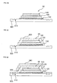
- FIG. 2A is a plane view illustrating an organic electroluminescent device according to a first embodiment of the present invention
- FIG. 2B is a view illustrating enlarged A part in FIG. 2A according to one embodiment of the present invention
- FIG. 2C is a view illustrating enlarged A part in FIG. 2A according to another embodiment of the present invention.
- the organic electroluminescent device of the present invention includes a substrate 300, pixels 30, a planarization layer 320 and a passivation layer 340.
- the substrate 300 has grooves 310 formed at the periphery of an active area in which the pixels 30 are formed.
- the pixels 30 are formed in the active area on the substrate 300 as shown in FIG. 2A. Additionally, the pixels 30 are formed by depositing in sequence an anode electrode layer 100, an organic layer 120 and a cathode electrode layer 140 on the substrate 300.
- the anode electrode layer 100 provides holes to the organic layer 120 in case a certain positive voltage is applied thereto, for example, indium tin oxide film (ITO film).
- ITO film indium tin oxide film
- the cathode electrode layer 140 provides electrons to the organic layer 120 in case a certain negative voltage is applied thereto.
- the organic layer 120 includes a hole transporting layer (HTL), an emitting layer (EML) and an electron transporting layer (ETL) formed in sequence on the anode electrode layer 100.
- HTL hole transporting layer
- EML emitting layer
- ETL electron transporting layer
- the HTL transports the holes provided from the anode electrode layer 100 into the EML
- the ETL transports the electrons provided from the cathode electrode layer 140 into the EML.
- the transported holes and electrons are recombined in the EML, and so a light having a predetermined wavelength is emitted from the EML.
- the planarization layer 320 covers the pixels 30, and is a non-conductive organic layer.
- the planarization layer 320 consisted of BenzoCyclo-Butene (BCB) or SiLK (Trademark of Dow Chemical Company) intensifies the adhesive force between the pixels 30 and the passivation layer 340.
- the passivation layer 340 as an inorganic layer is formed on the planarization 320 and the grooves 310, and prevents the permeation of oxygen ( O 2 ) or water ( H 2 O ) .
- the passivation layer 340 includes a first silicon oxide layer 340A, a silicon nitride layer 340B and a second silicon oxide layer 340C formed in sequence on the planarization layer 320 and the grooves 310, and so prevents oxygen ( O 2 ) or water ( H 2 O) from permeating into the inside of the passivation layer 340.
- the silicon nitride layer 340B is excellent to prevent the permeation of oxygen (O 2 ) or water ( H 2 O ) , but if formed thick, it may make the substrate 300 bend.
- the silicon nitride layer 340B should be formed thinly in order to prevent the permeation of oxygen ( O 2 ) or water (H 2 O).
- the passivation layer 340 includes a first silicon oxide layer 340A, a first silicon nitride layer 340B, a second silicon oxide layer 340C, a second silicon nitride layer 340D and a third silicon oxide layer 340E formed in sequence on the planarization layer 320 and the grooves 310.
- the passivation layer 340 may include at least one silicon nitride layer. However, it is desirable that the passivation layer 340 includes a plurality of thin silicon nitride layers as shown in FIG. 2C.
- the passivation layer 340 is formed on the substrate 300 to which the grooves 310 are formed, and thus the length of a permeation pathway through which oxygen ( O 2 ), water ( H 2 O ), etc. can permeate is augmented. As a result, oxygen ( O 2 ), water ( H 2 O ), etc. are not permeated into the inside of the passivation layer 340.
- the organic electroluminescent device does not include a cell cap unlike the conventional organic electroluminescent device.
- the organic electroluminescent device of the present invention is thinner than the conventional organic electroluminescent device. Accordingly, a mobile phone, etc. employing the organic electroluminescent device of the present invention may be thinner than a mobile phone, etc. employing the conventional organic electroluminescent device.
- FIG. 3A to FIG. 3D are plane views illustrating an organic electroluminescent device according to other embodiments of the present invention.
- grooves 310 are formed on a substrate 300 by etching the substrate 300 by using a certain mask 400.
- pixels 30 are formed on the substrate 300 as shown in FIG. 3B.
- a planarization layer 320 is formed on the substrate 300 to cover the pixels 30 as shown in FIG. 3C.
- the planarization layer 320 is formed when planarization material of non-conductive organic material is deposited on the pixels.
- the planarization layer 320 is formed by polishing the upper side of the planarization material when the material is deposited on the pixels 30.
- the passivation layer 340 is formed on the planarization layer 320 and the grooves 310 as shown in FIG. 3D.
- the grooves 310 are formed after the planarization layer 320 is deposited to cover the pixels 30.
- the grooves 310 should be formed in a vacuum atmosphere in order to prevent the permeation of oxygen ( O 2 ), water ( H 2 O ), etc.
- FIG. 4A is a plane view illustrating an organic electroluminescent device according to a second embodiment of the present invention
- FIG. 4B is a view illustrating enlarged B of FIG. 4A according to one embodiment of the present invention.
- FIG. 4C is a view illustrating enlarged B of FIG. 4A according to another embodiment of the present invention.
- the organic electroluminescent device of the present invention includes path extending sections 400, pixels 30, a planarization layer 420 and a passivation layer 440.
- the path extending sections 400 are formed on the substrate 10 at the periphery of the planarization layer 420 as shown in FIG. 4A.
- the path extending sections 400 have square shape or rectangular shape.
- the planarization layer 420 as a non-conductive organic layer covers the pixels 30.
- the planarization layer 420 consisted of BCB or SiLK intensifies the adhesive force between the pixels 30 and the passivation layer 440.
- the passivation layer 440 is formed on the substrate 10 on which the planarization layer 420 and the path extending sections 400 are formed.
- the passivation layer 440 as an inorganic layer prevents the permeation of oxygen ( O 2 ) or water ( H 2 O ).
- the passivation layer 440 includes a first silicon oxide layer 440A, a silicon nitride layer 440B and a second silicon oxide layer 440C formed in sequence on the substrate 10 on which the planarization layer 420 and the path extending sections 400 are formed.
- the passivation layer 440 includes a first silicon oxide layer 440A, a first silicon nitride layer 440B, a second silicon oxide layer 440C, a second silicon nitride layer 440D and a third silicon oxide layer 440E formed in sequence on the substrate 10 on which the planarization layer 320 and the path extending sections 400 are formed.
- the passivation layer 440 is formed on the substrate 10 on which the path extending sections 400 are formed, and thus the length of the permeation pathway through which oxygen (O 2 ), water (H 2 O), etc. are permeated is augmented. As a result, oxygen (O 2 ), water (H 2 O), etc. are not permeated into the inside of the passivation layer 440.
- the pixels 30 are formed on the substrate 10.
- planarization layer 420 is deposited to cover the pixels 30.
- the path extending sections 400 are deposited on the substrate 10 at the periphery of the planarization layer 420. In another embodiment, the path extending sections 400 are formed on the substrate 10 before the pixels 30 are formed on the substrate 10.
- the passivation layer 440 is formed on the substrate 10 on which the planarization layer 420 and the path extending sections 400 are deposited.
- FIG. 5 is a plane view illustrating an organic electroluminescent device according to a third embodiment of the present invention.
- the organic electroluminescent device of the present invention includes pixels 30, path extending sections 500, a planarization layer 520 and a passivation layer 540.
- planarization layer 520 and the passivation layer 540 are the same as those in the second embodiment, and so any further detailed descriptions concerning the same elements will be omitted.
- the path extending sections 500 have overhang shape, i.e. the upper base of the path extending sections 500 is longer than the lower base thereof as shown in FIG. 5, and extends the permeation pathway through which oxygen ( O 2 ) or water ( H 2 O ) permeates. As a result, oxygen ( O 2 ) or water ( H 2 O ) is not permeated into the inside of the passivation layer 540.
- the lower base of the path extending section 500 may be longer than the upper base thereof.
- path extending sections 500 are made up of the same material as a wall 180.
- An anode electrode layer 100 and an insulating layer 160 are deposited in sequence on a substrate 10.
- the path extending sections 500 are formed on the substrate 10 when the wall 180 is formed on the insulating layer 160.
- the path extending sections 500 may be formed before the pixels 30 are formed, or after the planarization layer 520 is formed.
- an organic layer 120 and a cathode electrode layer 140 are formed in sequence on the anode electrode layer 100, i.e. the pixels 30 are formed on the substrate 10.
- planarization layer 520 is formed on the pixels 30 to cover the pixels 30.
- the passivation layer 540 is formed on the substrate 10 on which the planarization layer 520 and the path extending sections 500 are formed.
- FIG. 6A is a plane view illustrating an organic electroluminescent device according to a fourth embodiment of the present invention.
- the organic electroluminescent device of the present invention includes pixels 30, a planarization layer 600, a permeation-preventing layer 620 and a passivation layer 640.
- the planarization layer 600 covers the pixels 30.
- the permeation-preventing layer 620 is formed on the planarization layer 600 to cover the planarization layer 600, and is made up of metal such as aluminium (Al), titanium (Ti) or titanium nitride (TiN).
- the metal is reactive to oxygen ( O 2 ) or water ( H 2 O ) .
- the metal is oxidized in case oxygen ( O 2 ) or water ( H 2 O ) is permeated, and so the permeation-preventing layer 620 is converted into an oxide layer.
- the density of the converted oxide layer is higher than that of the metal, and thus oxygen ( O 2 ) or water ( H 2 O ) is not diffused along the converted oxide layer.
- oxygen ( O 2 ) or water ( H 2 O ) is not permeated into the inside of the permeation-preventing layer 620.
- the passivation layer 640 is formed on the permeation-preventing layer 620.
- the passivation layer 640 is formed by depositing in sequence a first silicon oxide layer, a silicon nitride layer and a second silicon oxide layer on the permeation-preventing section 620.
- the passivation layer 640 is formed by depositing in sequence a first silicon oxide layer, a first silicon nitride layer, a second silicon oxide layer, a second silicon nitride layer and a third silicon oxide layer on the permeation-preventing layer 620.
- the pixels 30 are formed on the substrate 10, and then the planarization layer 600 is formed on the pixels 30 to cover the pixels 30.
- the permeation-preventing layer 620 is formed on the planarization layer 600 to cover the planarization layer 600, and then the passivation layer 640 is formed on the permeation-preventing layer 620.
- the organic electroluminescent device of the present invention includes the permeation-preventing layer 620 converted into an oxide layer in case oxygen (O 2 ) or water (H 2 O) is permeated, unlike the conventional organic electroluminescent device. Hence, oxygen (O 2 ) or water (H 2 O) permeated after the permeation-preventing layer 620 is converted into the oxide layer is not permeated into the inside of the permeation-preventing layer 620.
- FIG. 6B is a plane view illustrating an organic electroluminescent device according to a fifth embodiment of the present invention.
- the organic electroluminescent device of the present invention includes pixels 30, a planarization layer 600, a permeation-preventing layer 660 and a passivation layer 640.
- the permeation-preventing layer 660 as an oxide layer is formed by forming a metal layer such as Al, Ti or TiN on the planarization layer 600, and then oxidizing the metal layer in an oxygen atmosphere.
- the permeation-preventing layer 660 is formed before oxygen ( O 2 ) or water (H 2 O ) is permeated, unlike the permeation-preventing layer 320 in the fourth embodiment.
- FIG. 7A is a plane view illustrating an organic electroluminescent device according to a sixth embodiment of the present invention.
- the organic electroluminescent device of the present invention includes a substrate 700, pixels 30, a planarization layer 740, a permeation-preventing layer 760 and a passivation layer 780.
- the substrate 700 has grooves 720 at the periphery of an active area as shown in FIG. 7A.
- the planarization layer 740 is formed on the pixels 30 to cover the pixels 30, and is made up of non-conductive organic layer such as BCB or SiLK.
- the permeation-preventing layer 760 is formed to cover the planarization layer 740 and grooves 720, and is made up of metal such as Al, Ti or TiN.
- the metal is reactive to oxygen ( O 2 ) or water ( H 2 O ).
- the metal is oxidized in case oxygen ( O 2 ) or water ( H 2 O ) is permeated, and so the permeation-preventing layer 760 is converted into an oxide layer.
- the density of the converted oxide layer is higher than that of the metal, and thus oxygen (O 2 ) or water (H 2 O) is not diffused along the converted oxide layer.
- oxygen (O 2 ) or water ( H 2 O ) is not permeated into the inside of the permeation-preventing layer 760.
- the passivation layer 780 is formed on the permeation-preventing layer 760.
- the passivation layer 780 is formed by depositing in sequence a first silicon oxide layer, a silicon nitride layer and a second silicon oxide layer on the permeation-preventing section 760.
- the passivation layer 780 is formed by depositing in sequence a first silicon oxide layer, a first silicon nitride layer, a second silicon oxide layer, a second silicon nitride layer and a third silicon oxide layer on the permeation-preventing layer 760.
- the grooves 720 are formed on the substrate 700 by etching the substrate 700 by using a certain mask.
- the pixels 30 are formed on the substrate 700.
- planarization layer 740 is deposited on the pixels 30 to cover the pixels 30.
- the permeation-preventing layer 760 is formed on the substrate 700 on which the planarization 740 and the grooves 720 are formed.
- the passivation layer 780 is formed on the permeation-preventing layer 760.
- the grooves 720 are formed after the planarization layer 740 is deposited on the pixels 30.
- the grooves 720 should be formed in a vacuum atmosphere in order to prevent the permeation of oxygen (O 2 ), water ( H 2 O ) , etc.
- FIG. 7B is a plane view illustrating an organic electroluminescent device according to a seventh embodiment of the present invention.
- the organic electroluminescent device of the present invention includes a substrate 700, pixels 30, a planarization layer 740, a permeation-preventing layer 790 and a passivation layer 780.
- the permeation-preventing layer 790 as an oxide layer is formed by forming a metal layer such as Al, Ti or TiN to cover the substrate 700 on which the planarization layer 740 and the grooves 720 are formed, and then oxidizing the metal layer in an oxygen atmosphere.
- the permeation-preventing layer 790 is formed before oxygen ( O 2 ) or water ( H 2 O ) is permeated, unlike the permeation-preventing layer 760 in the sixth embodiment.
- FIG. 8A is a plane view illustrating an organic electroluminescent device according to an eighth embodiment of the present invention.
- the organic electroluminescent device of the present invention includes path extending sections 820, pixels 30, a planarization layer 840, a permeation-preventing layer 860 and a passivation layer 880.
- the path extending sections 820 are formed on the substrate 800 at the periphery of an active area in which the pixels 30 are formed.
- the path extending sections 820 have square shape, rectangular shape, or overhang shape.
- the planarization layer 840 covers the pixels 30, and is made up of non-conductive organic film such as BCB or SiLK.
- the permeation-preventing layer 860 is formed to cover the planarization layer 840 and the path extending sections 820, and is made up of metal such as Al, Ti or TiN.
- the metal is reactive to oxygen (O 2 ) or water (H 2 O).
- the metal is oxidized in case oxygen (O 2 ) or water (H 2 O) is permeated, and so the permeation-preventing layer 860 is converted into an oxide layer.
- the density of the converted oxide layer is higher than that of the metal, and thus oxygen ( O 2 ) or water ( H 2 O ) is not diffused along the converted oxide layer.
- oxygen ( O 2 ) or water ( H 2 O ) is not permeated into the inside of the permeation-preventing layer 860.
- the passivation layer 880 as an inorganic layer is formed on the permeation-preventing layer 860.
- the pixels 30 are formed on the substrate 800. Subsequently, the planarization layer 840 is deposited to cover the pixels 30.
- the path extending sections 820 are formed at the periphery of the planarization layer 840 on the substrate 800.
- the path extending sections 820 may be formed before the pixels 30 are formed on the substrate 800.
- the path extending sections 820 may be formed on the substrate 800 when a wall 180 is formed.
- the permeation-preventing layer 860 is formed on the substrate 800 on which the planarization layer 840 and the path extending layers 820 are formed.
- the passivation layer 880 is formed on the permeation-preventing layer 860.
- FIG. 8B is a plane view illustrating an organic electroluminescent device according to a ninth embodiment of the present invention.
- the organic electroluminescent device of the present invention includes pixels 30, a planarization layer 840, a permeation-preventing layer 890 and a passivation layer 880.
- the permeation-preventing layer 890 as an oxide layer is formed by forming a metal layer such as Al, Ti or TiN to cover the substrate 800 on which the planarization layer 840 and the path extending sections 820 are formed, and then oxidizing the metal layer in an oxygen atmosphere.
- the permeation-preventing layer 890 is formed before oxygen ( O 2 ) or water ( H 2 O ) is permeated, unlike the permeation-preventing layer 860 in the eighth embodiment.
Landscapes
- Physics & Mathematics (AREA)
- Optics & Photonics (AREA)
- Electroluminescent Light Sources (AREA)
Abstract
Description
- This application claims priorities from Korean Patent Application Nos. 2004-84502 and 2004-84505, filed on October 21; 2004, 2004-85201, filed on October 25, 2004; and 2004-94954 and 2004-94957, filed on November 19, 2004, the contents of which are incorporated herein by reference in their entirety.
- The present invention relates to an organic electroluminescent device and a method of manufacturing the same. More particularly, the present invention relates to a thin organic electroluminescent device capable of preventing permeation of oxygen or water and a method of manufacturing the same.
- An organic electroluminescent device as self light-emitting device emits a light having a predetermined wavelength when a certain voltage is applied thereto.
- FIG. 1A is a plane view illustrating a conventional first organic electroluminescent device.
- In FIG. 1A, the organic electroluminescent device includes a plurality of
pixels 30, agetter 50 and acell cap 70. - Each of the
pixels 30 includes ananode electrode layer 100, anorganic layer 120 and acathode electrode layer 140 formed in sequence on asubstrate 10. In case a positive voltage and a negative voltage are respectively applied to theanode electrode layer 100 and thecathode electrode layer 140, a light having a certain wavelength is emitted from theorganic layer 120. - The
getter 50 is attached to thecell cap 70, and removes oxygen (O 2 ) or water (H 2 O) in the organic electroluminescent device. - The
cell cap 70 covers thepixels 30 so that oxygen (O 2 ), water (H 2 O), etc. are not permeated into the inside of thecell cap 70. In this case, thegetter 50 should not be contacted to thecathode electrode layer 140. Therefore, a space is required between thegetter 50 and thecathode electrode layer 140, and so the thickness of the first organic electroluminescent device is increased. - Recently, a mobile phone, etc. employing an organic electroluminescent device tends to be miniaturized. Hence, the thickness of the organic electroluminescent device also should be reduced. However, the first organic electroluminescent device includes the
cell cap 70 to which thegetter 50 is attached, and so the thickness of a mobile phone employing the conventional first organic electroluminescent device could not be reduced. - Accordingly, the following second organic electroluminescent device was developed.
- FIG. 1B is a plane view illustrating a conventional second organic electroluminescent device.
- In FIG. 1B, the second organic electroluminescent device includes
pixels 30, aplanarization layer 200 and apassivation layer 220. - The
planarization layer 200 is formed on thepixels 30, thereby intensifying the adhesive force between thepixels 30 and thepassivation layer 220. - The
passivation layer 220 is formed on theplanarization layer 200 to prevent oxygen (O 2 ), water (H 2 O), etc. permeating into the inside of thepassivation layer 220. However, the thickness of edge part of thepassivation layer 220 which is attached to thesubstrate 10 is thin, and thus oxygen (O 2 ), water (H 2 O), etc. could be permeated into the inside of theplanarization layer 200. As a result, a part of thepixels 30 may not emit a light. - Accordingly, there has been a need for another organic electroluminescent device that can prevent the permeation of oxygen (O 2 ), water (H 2 O), etc. and is thin.
- It is a feature of the present invention to provide an organic electroluminescent device capable of preventing the permeation of oxygen (O 2 ), water (H 2 O), etc. and a method of manufacturing the same.
- An organic electroluminescent device according to a first embodiment of the present invention includes a substrate, a plurality of pixels and a planarization layer. The substrate has grooves formed at the periphery of an active area. The pixels are formed in the active area. The planarization layer covers the pixels on the substrate. The passivation layer covers the planarization layer and the grooves.
- An organic electroluminescent device according to a second embodiment of the present invention includes a substrate, a planarization layer, a permeation-preventing layer and a passivation layer. The substrate has a plurality of pixels formed in active area. The planarization layer covers the pixels. The permeation-preventing layer covers the planarization layer. The passivation layer is formed on the permeation preventing layer.
- An organic electroluminescent device having a plurality of pixels formed on a substrate according to a third embodiment of the present invention includes a planarization layer, a plurality of path extending sections and a passivation layer. The planarization layer covers the pixels. The path extending sections are formed on the substrate at the periphery of the planarization layer. The passivation layer covers the planarization layer and the path extending sections.
- A method of manufacturing an organic electroluminescent device according to a first embodiment of the present invention includes producing a substrate having a plurality of grooves at the periphery of an active area by patterning the subatate; forming a plurality of pixels in the active area; forming a planarization layer on the pixels so that the pixels are covered by the planarization layer; and forming a passivation layer on the planarization layer and the grooves so that the planarization layer and the grooves are covered by the passivation layer.
- A method of manufacturing an organic electroluminescent device having a plurality of pixels formed on a substrate according to a second embodiment of the present invention includes forming a planarization layer on the pixels so that the pixels are covered by the planarization layer; forming a plurality of path extending sections on the substrate at the periphery of an area in which the planarization layer is formed; and forming a passivation layer on the planarization layer and the path extending sections.
- A method of manufacturing an organic electroluminescent device having a plurality of pixels according to a third embodiment of the present invention includes forming a planarization layer on the pixels so that the pixels are covered by the planarization layer; forming a permeation-preventing layer on the planarization layer so that the planarization layer is covered by the permeation-preventing layer; and forming a passivation layer on the permeation-preventing layer.
- As described above, the present organic electroluminescent device and a method of manufacturing the same includes grooves or path extending sections, and thus oxygen (O 2 ), water (H 2 O), etc. are not permeated into the inside of a passivation layer.
- In addition, the present organic electroluminescent device and a method of manufacturing the same includes a permeation-preventing layer, and thus ( O 2), water (H 2 O), etc. are not permeated into the inside of the permeation-preventing layer.
- The above and other features and advantages of the present invention will become readily apparent by reference to the following detailed description when considered in conjunction with the accompanying drawings wherein:
- FIG. 1A is a plane view illustrating a conventional first organic electroluminescent device;
- FIG. 1B is a plane view illustrating a conventional second organic electroluminescent device;
- FIG. 2A is a plane view illustrating an organic electroluminescent device according to a first embodiment of the present invention;
- FIG. 2B is a view illustrating enlarged A part in FIG. 2A according to one embodiment of the present invention;
- FIG. 2C is a view illustrating enlarged A part in FIG. 2A according to another embodiment of the present invention;
- FIG. 3A to FIG. 3D are plane views illustrating an organic electroluminescent device according to other embodiments of the present invention;
- FIG. 4A is a plane view illustrating an organic electroluminescent device according to a second embodiment of the present invention;
- FIG. 4B is a view illustrating the enlarged B of FIG. 4A according to one embodiment of the present invention;
- FIG. 4C is a view illustrating the enlarged B of FIG. 4A according to another embodiment of the present invention;
- FIG. 5 is a plane view illustrating an organic electroluminescent device according to a third embodiment of the present invention;
- FIG. 6A is a plane view illustrating an organic electroluminescent device according to a fourth embodiment of the present invention;
- FIG. 6B is a plane view illustrating an organic electroluminescent device according to a fifth embodiment of the present invention;
- FIG. 7A is a plane view illustrating an organic electroluminescent device according to a sixth embodiment of the present invention;
- FIG. 7B is a plane view illustrating an organic electroluminescent device according to a seventh embodiment of the present invention;
- FIG. 8A is a plane view illustrating an organic electroluminescent device according to an eighth embodiment of the present invention; and
- FIG. 8B is a plane view illustrating an organic electroluminescent device according to a ninth embodiment of the present invention.
- Hereinafter, the preferred embodiments of the present invention will be explained in more detail with reference to the accompanying drawings.
- FIG. 2A is a plane view illustrating an organic electroluminescent device according to a first embodiment of the present invention, and FIG. 2B is a view illustrating enlarged A part in FIG. 2A according to one embodiment of the present invention. In addition, FIG. 2C is a view illustrating enlarged A part in FIG. 2A according to another embodiment of the present invention.
- In FIG. 2A to FIG. 2C, the organic electroluminescent device of the present invention includes a
substrate 300,pixels 30, aplanarization layer 320 and apassivation layer 340. - The
substrate 300 hasgrooves 310 formed at the periphery of an active area in which thepixels 30 are formed. - The
pixels 30 are formed in the active area on thesubstrate 300 as shown in FIG. 2A. Additionally, thepixels 30 are formed by depositing in sequence ananode electrode layer 100, anorganic layer 120 and acathode electrode layer 140 on thesubstrate 300. - The
anode electrode layer 100 provides holes to theorganic layer 120 in case a certain positive voltage is applied thereto, for example, indium tin oxide film (ITO film). - The
cathode electrode layer 140 provides electrons to theorganic layer 120 in case a certain negative voltage is applied thereto. - The
organic layer 120 includes a hole transporting layer (HTL), an emitting layer (EML) and an electron transporting layer (ETL) formed in sequence on theanode electrode layer 100. In case the positive voltage and the negative voltage are respectively applied to theanode electrode layer 100 and thecathode electrode layer 140, the HTL transports the holes provided from theanode electrode layer 100 into the EML, and the ETL transports the electrons provided from thecathode electrode layer 140 into the EML. The transported holes and electrons are recombined in the EML, and so a light having a predetermined wavelength is emitted from the EML. - The
planarization layer 320 covers thepixels 30, and is a non-conductive organic layer. For example, theplanarization layer 320 consisted of BenzoCyclo-Butene (BCB) or SiLK (Trademark of Dow Chemical Company) intensifies the adhesive force between thepixels 30 and thepassivation layer 340. - The
passivation layer 340 as an inorganic layer is formed on theplanarization 320 and thegrooves 310, and prevents the permeation of oxygen (O 2 ) or water (H 2 O). - In FIG. 2B, the
passivation layer 340 according to one embodiment of the present invention includes a first silicon oxide layer 340A, a silicon nitride layer 340B and a second silicon oxide layer 340C formed in sequence on theplanarization layer 320 and thegrooves 310, and so prevents oxygen (O 2 ) or water (H 2 O) from permeating into the inside of thepassivation layer 340. Here, the silicon nitride layer 340B is excellent to prevent the permeation of oxygen (O2) or water (H 2 O), but if formed thick, it may make thesubstrate 300 bend. Hence, the silicon nitride layer 340B should be formed thinly in order to prevent the permeation of oxygen (O 2 ) or water (H 2 O). - In FIG. 2C, the
passivation layer 340 according to another embodiment of the present invention includes a first silicon oxide layer 340A, a first silicon nitride layer 340B, a second silicon oxide layer 340C, a second silicon nitride layer 340D and a third silicon oxide layer 340E formed in sequence on theplanarization layer 320 and thegrooves 310. - In brief, the
passivation layer 340 may include at least one silicon nitride layer. However, it is desirable that thepassivation layer 340 includes a plurality of thin silicon nitride layers as shown in FIG. 2C. - In the organic electroluminescent device of the present invention, the
passivation layer 340 is formed on thesubstrate 300 to which thegrooves 310 are formed, and thus the length of a permeation pathway through which oxygen (O 2 ), water (H 2 O), etc. can permeate is augmented. As a result, oxygen (O 2), water (H 2 O), etc. are not permeated into the inside of thepassivation layer 340. - In addition, the organic electroluminescent device does not include a cell cap unlike the conventional organic electroluminescent device. Thus, the organic electroluminescent device of the present invention is thinner than the conventional organic electroluminescent device. Accordingly, a mobile phone, etc. employing the organic electroluminescent device of the present invention may be thinner than a mobile phone, etc. employing the conventional organic electroluminescent device.
- FIG. 3A to FIG. 3D are plane views illustrating an organic electroluminescent device according to other embodiments of the present invention.
- In FIG. 3A,
grooves 310 are formed on asubstrate 300 by etching thesubstrate 300 by using acertain mask 400. - Subsequently,
pixels 30 are formed on thesubstrate 300 as shown in FIG. 3B. - Then, a
planarization layer 320 is formed on thesubstrate 300 to cover thepixels 30 as shown in FIG. 3C. Specifically, theplanarization layer 320 is formed when planarization material of non-conductive organic material is deposited on the pixels. In another embodiment, theplanarization layer 320 is formed by polishing the upper side of the planarization material when the material is deposited on thepixels 30. - Subsequently, the
passivation layer 340 is formed on theplanarization layer 320 and thegrooves 310 as shown in FIG. 3D. - In a method of manufacturing the organic electroluminescent device according to another embodiment of the present invention, the
grooves 310 are formed after theplanarization layer 320 is deposited to cover thepixels 30. In this case, thegrooves 310 should be formed in a vacuum atmosphere in order to prevent the permeation of oxygen (O 2 ), water (H 2 O), etc. - FIG. 4A is a plane view illustrating an organic electroluminescent device according to a second embodiment of the present invention, and FIG. 4B is a view illustrating enlarged B of FIG. 4A according to one embodiment of the present invention. Also, FIG. 4C is a view illustrating enlarged B of FIG. 4A according to another embodiment of the present invention.
- In FIG. 4A to FIG. 4C, the organic electroluminescent device of the present invention includes
path extending sections 400,pixels 30, aplanarization layer 420 and apassivation layer 440. - The
path extending sections 400 are formed on thesubstrate 10 at the periphery of theplanarization layer 420 as shown in FIG. 4A. Here, thepath extending sections 400 have square shape or rectangular shape. - The
planarization layer 420 as a non-conductive organic layer covers thepixels 30. For example, theplanarization layer 420 consisted of BCB or SiLK intensifies the adhesive force between thepixels 30 and thepassivation layer 440. - The
passivation layer 440 is formed on thesubstrate 10 on which theplanarization layer 420 and thepath extending sections 400 are formed. In addition, thepassivation layer 440 as an inorganic layer prevents the permeation of oxygen (O 2 ) or water (H 2 O). - In FIG. 4B, the
passivation layer 440 according to one embodiment of the present invention includes a first silicon oxide layer 440A, a silicon nitride layer 440B and a secondsilicon oxide layer 440C formed in sequence on thesubstrate 10 on which theplanarization layer 420 and thepath extending sections 400 are formed. - In FIG. 4C, the
passivation layer 440 according to another embodiment of the present invention includes a first silicon oxide layer 440A, a first silicon nitride layer 440B, a secondsilicon oxide layer 440C, a second silicon nitride layer 440D and a third silicon oxide layer 440E formed in sequence on thesubstrate 10 on which theplanarization layer 320 and thepath extending sections 400 are formed. - In the organic electroluminescent device of the present invention, the
passivation layer 440 is formed on thesubstrate 10 on which thepath extending sections 400 are formed, and thus the length of the permeation pathway through which oxygen (O 2 ), water (H 2 O), etc. are permeated is augmented. As a result, oxygen (O 2 ), water (H 2 O), etc. are not permeated into the inside of thepassivation layer 440. - Hereinafter, a process of manufacturing the organic electroluminescent device will be described in detail.
- The
pixels 30 are formed on thesubstrate 10. - Subsequently, the
planarization layer 420 is deposited to cover thepixels 30. - Then, the
path extending sections 400 are deposited on thesubstrate 10 at the periphery of theplanarization layer 420. In another embodiment, thepath extending sections 400 are formed on thesubstrate 10 before thepixels 30 are formed on thesubstrate 10. - Subsequently, the
passivation layer 440 is formed on thesubstrate 10 on which theplanarization layer 420 and thepath extending sections 400 are deposited. - FIG. 5 is a plane view illustrating an organic electroluminescent device according to a third embodiment of the present invention.
- In FIG. 5, the organic electroluminescent device of the present invention includes
pixels 30,path extending sections 500, aplanarization layer 520 and apassivation layer 540. - The
planarization layer 520 and thepassivation layer 540 are the same as those in the second embodiment, and so any further detailed descriptions concerning the same elements will be omitted. - The
path extending sections 500 have overhang shape, i.e. the upper base of thepath extending sections 500 is longer than the lower base thereof as shown in FIG. 5, and extends the permeation pathway through which oxygen (O 2) or water (H 2 O) permeates. As a result, oxygen (O 2 ) or water (H 2 O) is not permeated into the inside of thepassivation layer 540. In another embodiment, the lower base of thepath extending section 500 may be longer than the upper base thereof. - In addition, the
path extending sections 500 are made up of the same material as awall 180. - Hereinafter, a process of manufacturing this organic electroluminescent device will be described in detail.
- An
anode electrode layer 100 and an insulatinglayer 160 are deposited in sequence on asubstrate 10. - Subsequently, the
path extending sections 500 are formed on thesubstrate 10 when thewall 180 is formed on the insulatinglayer 160. In another embodiment, thepath extending sections 500 may be formed before thepixels 30 are formed, or after theplanarization layer 520 is formed. - Then, an
organic layer 120 and acathode electrode layer 140 are formed in sequence on theanode electrode layer 100, i.e. thepixels 30 are formed on thesubstrate 10. - Subsequently, the
planarization layer 520 is formed on thepixels 30 to cover thepixels 30. - Then, the
passivation layer 540 is formed on thesubstrate 10 on which theplanarization layer 520 and thepath extending sections 500 are formed. - FIG. 6A is a plane view illustrating an organic electroluminescent device according to a fourth embodiment of the present invention.
- In FIG. 6A, the organic electroluminescent device of the present invention includes
pixels 30, aplanarization layer 600, a permeation-preventinglayer 620 and apassivation layer 640. - The
planarization layer 600 covers thepixels 30. - The permeation-preventing
layer 620 is formed on theplanarization layer 600 to cover theplanarization layer 600, and is made up of metal such as aluminium (Al), titanium (Ti) or titanium nitride (TiN). Here, the metal is reactive to oxygen (O 2 ) or water (H 2 O). Hence, the metal is oxidized in case oxygen (O 2 ) or water (H 2 O) is permeated, and so the permeation-preventinglayer 620 is converted into an oxide layer. The density of the converted oxide layer is higher than that of the metal, and thus oxygen (O 2 ) or water (H 2 O) is not diffused along the converted oxide layer. As a result, after the oxide layer is formed, oxygen (O 2 ) or water (H 2 O) is not permeated into the inside of the permeation-preventinglayer 620. - The
passivation layer 640 is formed on the permeation-preventinglayer 620. - The
passivation layer 640 according to one embodiment of the present invention is formed by depositing in sequence a first silicon oxide layer, a silicon nitride layer and a second silicon oxide layer on the permeation-preventingsection 620. - The
passivation layer 640 according to another embodiment of the present invention is formed by depositing in sequence a first silicon oxide layer, a first silicon nitride layer, a second silicon oxide layer, a second silicon nitride layer and a third silicon oxide layer on the permeation-preventinglayer 620. - Hereinafter, a method of manufacturing the organic electroluminescent device will be described in detail.
- The
pixels 30 are formed on thesubstrate 10, and then theplanarization layer 600 is formed on thepixels 30 to cover thepixels 30. - Subsequently, the permeation-preventing
layer 620 is formed on theplanarization layer 600 to cover theplanarization layer 600, and then thepassivation layer 640 is formed on the permeation-preventinglayer 620. - The organic electroluminescent device of the present invention includes the permeation-preventing
layer 620 converted into an oxide layer in case oxygen (O 2 ) or water (H 2 O) is permeated, unlike the conventional organic electroluminescent device. Hence, oxygen (O 2 ) or water (H 2 O) permeated after the permeation-preventinglayer 620 is converted into the oxide layer is not permeated into the inside of the permeation-preventinglayer 620. - FIG. 6B is a plane view illustrating an organic electroluminescent device according to a fifth embodiment of the present invention.
- In FIG. 6B, the organic electroluminescent device of the present invention includes
pixels 30, aplanarization layer 600, a permeation-preventinglayer 660 and apassivation layer 640. - Since the elements of the present embodiment except the permeation-preventing
layer 660 are the same as those in the first embodiment, any further detailed descriptions concerning the same elements will be omitted. - The permeation-preventing
layer 660 as an oxide layer is formed by forming a metal layer such as Al, Ti or TiN on theplanarization layer 600, and then oxidizing the metal layer in an oxygen atmosphere. In other words, the permeation-preventinglayer 660 is formed before oxygen (O 2 ) or water (H 2 O) is permeated, unlike the permeation-preventinglayer 320 in the fourth embodiment. - FIG. 7A is a plane view illustrating an organic electroluminescent device according to a sixth embodiment of the present invention.
- In FIG. 7A, the organic electroluminescent device of the present invention includes a
substrate 700,pixels 30, aplanarization layer 740, a permeation-preventinglayer 760 and apassivation layer 780. - The
substrate 700 hasgrooves 720 at the periphery of an active area as shown in FIG. 7A. - The
planarization layer 740 is formed on thepixels 30 to cover thepixels 30, and is made up of non-conductive organic layer such as BCB or SiLK. - The permeation-preventing
layer 760 is formed to cover theplanarization layer 740 andgrooves 720, and is made up of metal such as Al, Ti or TiN. Here, the metal is reactive to oxygen (O 2 ) or water (H 2 O). Hence, the metal is oxidized in case oxygen (O 2 ) or water (H 2 O) is permeated, and so the permeation-preventinglayer 760 is converted into an oxide layer. The density of the converted oxide layer is higher than that of the metal, and thus oxygen (O 2 ) or water (H 2 O) is not diffused along the converted oxide layer. As a result, after the oxide layer is formed, oxygen (O 2 ) or water (H 2 O) is not permeated into the inside of the permeation-preventinglayer 760. - The
passivation layer 780 is formed on the permeation-preventinglayer 760. - The
passivation layer 780 according to another embodiment of the present invention is formed by depositing in sequence a first silicon oxide layer, a silicon nitride layer and a second silicon oxide layer on the permeation-preventingsection 760. - The
passivation layer 780 according to another embodiment of the present invention is formed by depositing in sequence a first silicon oxide layer, a first silicon nitride layer, a second silicon oxide layer, a second silicon nitride layer and a third silicon oxide layer on the permeation-preventinglayer 760. - Hereinafter, a process of manufacturing the organic electroluminescent device will be described in detail.
- The
grooves 720 are formed on thesubstrate 700 by etching thesubstrate 700 by using a certain mask. - Subsequently, the
pixels 30 are formed on thesubstrate 700. - Then, the
planarization layer 740 is deposited on thepixels 30 to cover thepixels 30. - Subsequently, the permeation-preventing
layer 760 is formed on thesubstrate 700 on which theplanarization 740 and thegrooves 720 are formed. - Then, the
passivation layer 780 is formed on the permeation-preventinglayer 760. - In a method of manufacturing the organic electroluminescent device according to another embodiment of the present invention, the
grooves 720 are formed after theplanarization layer 740 is deposited on thepixels 30. In this case, thegrooves 720 should be formed in a vacuum atmosphere in order to prevent the permeation of oxygen (O 2 ), water (H 2 O), etc. - FIG. 7B is a plane view illustrating an organic electroluminescent device according to a seventh embodiment of the present invention.
- In FIG. 7B, the organic electroluminescent device of the present invention includes a
substrate 700,pixels 30, aplanarization layer 740, a permeation-preventinglayer 790 and apassivation layer 780. - Since the elements of the present invention except the permeation-preventing
layer 790 are the same as those in the sixth embodiment, any further detailed descriptions concerning the same elements will be omitted. - The permeation-preventing
layer 790 as an oxide layer is formed by forming a metal layer such as Al, Ti or TiN to cover thesubstrate 700 on which theplanarization layer 740 and thegrooves 720 are formed, and then oxidizing the metal layer in an oxygen atmosphere. In other words, the permeation-preventinglayer 790 is formed before oxygen (O 2 ) or water (H 2 O) is permeated, unlike the permeation-preventinglayer 760 in the sixth embodiment. - FIG. 8A is a plane view illustrating an organic electroluminescent device according to an eighth embodiment of the present invention.
- In FIG. 8A, the organic electroluminescent device of the present invention includes
path extending sections 820,pixels 30, aplanarization layer 840, a permeation-preventinglayer 860 and apassivation layer 880. - The
path extending sections 820 are formed on thesubstrate 800 at the periphery of an active area in which thepixels 30 are formed. Here, thepath extending sections 820 have square shape, rectangular shape, or overhang shape. - The
planarization layer 840 covers thepixels 30, and is made up of non-conductive organic film such as BCB or SiLK. - The permeation-preventing
layer 860 is formed to cover theplanarization layer 840 and thepath extending sections 820, and is made up of metal such as Al, Ti or TiN. Here, the metal is reactive to oxygen (O 2 ) or water (H 2 O). Hence, the metal is oxidized in case oxygen (O 2 ) or water (H 2 O) is permeated, and so the permeation-preventinglayer 860 is converted into an oxide layer. The density of the converted oxide layer is higher than that of the metal, and thus oxygen (O 2 ) or water (H 2 O) is not diffused along the converted oxide layer. As a result, after the oxide layer is formed, oxygen (O 2 ) or water (H 2 O) is not permeated into the inside of the permeation-preventinglayer 860. - The
passivation layer 880 as an inorganic layer is formed on the permeation-preventinglayer 860. - Hereinafter, a process of manufacturing the organic electroluminescent device of the present invention will be described in detail.
- The
pixels 30 are formed on thesubstrate 800. Subsequently, theplanarization layer 840 is deposited to cover thepixels 30. - Then, the
path extending sections 820 are formed at the periphery of theplanarization layer 840 on thesubstrate 800. In another embodiment, thepath extending sections 820 may be formed before thepixels 30 are formed on thesubstrate 800. Thepath extending sections 820 may be formed on thesubstrate 800 when awall 180 is formed. - Subsequently, the permeation-preventing
layer 860 is formed on thesubstrate 800 on which theplanarization layer 840 and thepath extending layers 820 are formed. - Then, the
passivation layer 880 is formed on the permeation-preventinglayer 860. - FIG. 8B is a plane view illustrating an organic electroluminescent device according to a ninth embodiment of the present invention.
- In FIG. 8B, the organic electroluminescent device of the present invention includes
pixels 30, aplanarization layer 840, a permeation-preventinglayer 890 and apassivation layer 880. - Since the elements of the present invention except the permeation-preventing
layer 890 are the same as those in the eighth embodiment, any further detailed descriptions will be omitted. - The permeation-preventing
layer 890 as an oxide layer is formed by forming a metal layer such as Al, Ti or TiN to cover thesubstrate 800 on which theplanarization layer 840 and thepath extending sections 820 are formed, and then oxidizing the metal layer in an oxygen atmosphere. In other words, the permeation-preventinglayer 890 is formed before oxygen (O 2 ) or water (H 2 O) is permeated, unlike the permeation-preventinglayer 860 in the eighth embodiment. - From the preferred embodiments for the present invention, it is noted that modifications and variations can be made by a person skilled in the art in light of the above teachings. Therefore, it should be understood that changes may be made for a particular embodiment of the present invention within the scope and spirit of the present invention outlined by the appended claims.
Claims (29)
- An organic electroluminescent device comprising:a substrate having grooves formed at the periphery of an active area;a plurality of pixels formed in the active area;a planarization layer covering the pixels on the substrate; anda passivation layer covering the planarization layer and the grooves.
- The organic electroluminescent device of claim 1, wherein the planarization layer is a non-conducting organic layer.
- The organic electroluminescent device of claim 2, wherein the planarization layer contains BenzoCyclo-Butene or SiLK.
- The organic electroluminescent device of claim 1, wherein the passivation layer is an inorganic layer as a layer for preventing oxygen and water.
- An organic electroluminescent device comprising:a substrate including a plurality of pixels formed in an active area;a planarization layer covering the pixels;a permeation-preventing layer covering the planarization layer; anda passivation layer formed on the permeation preventing layer.
- The organic electroluminescent device of claim 5, wherein groove is formed at the periphery of the active area on the substrate, and wherein the permeation-preventing section covers the groove.
- The organic electroluminescent device of claim 5, further including:a path extending section formed at the periphery of the active area,wherein the permeation-preventing section covers the path-extending section.
- The organic electroluminescent device of claim 8, wherein the permeation-preventing layer contains aluminium (Al), titanium (Ti), or titanium nitride (TiN).
- The organic electroluminescent device of claim 5, wherein the permeation-preventing layer is an oxide layer.
- An organic electroluminescent device having a plurality of pixels formed on a substrate comprising:a planarization layer covering the pixels;a plurality of path extending sections formed on the substrate at the periphery of the planarization layer; anda passivation layer covering the planarization layer and the path extending sections.
- The organic electroluminescent device of claim 10, wherein each of the path extending sections has a trapezoid shape.
- The organic electroluminescent device of claim 10, wherein each of the path extending sections has a rectangular shape.
- The organic electroluminescent device of claim 10, further including a permeation-preventing layer formed between the planarization layer, the path extending sections and the passivation layer.
- The organic electroluminescent device of claim 13, wherein the permeation preventing layer includes aluminium (Al), titanium (Ti), or titanium nitride (TiN).
- The organic electroluminescent device of claim 13, wherein the permeation-preventing layer is an oxide layer.
- A method of manufacturing an organic electroluminescent device comprising:producing a substrate having a plurality of grooves at the periphery of an active area by patterning the subatate;forming a plurality of pixels in the active area;forming a planarization layer on the pixels so that the pixels are covered by the planarization layer; andforming a passivation layer on the planarization layer and the grooves so that the planarization layer and the grooves are covered by the passivation layer.
- The method of manufacturing an organic electroluminescent device of claim 16, wherein forming the planarization layer includes:depositing a planarization material on the pixels so that the pixels are covered by the planarization material; andpolishing an upper side of the deposited planarization material.
- The method of manufacturing an organic electroluminescent device of claim 17, wherein the grooves are formed by patterning the substrate on which the planarization layer is formed.
- The method of manufacturing an organic electroluminescent device of claim 18, wherein the grooves are formed in a vacuum atmosphere.
- The method of manufacturing an organic electroluminescent device of claim 16, further including:forming a permeation-preventing layer on the planarization layer and the grooves so that the permeation-preventing layer is located between the planarization layer, the grooves and the passivation layer.
- The method of manufacturing an organic electroluminescent device of claim 20, wherein forming the permeation-preventing layer includes:forming a metal layer on the planarization layer and the grooves; andoxidizing the metal layer in an oxygen atmosphere to form an oxide layer.
- A method of manufacturing an organic electroluminescent device having a plurality of pixels formed on a substrate comprising:forming a planarization layer on the pixels so that the pixels are covered by the planarization layer;forming a plurality of path extending sections on the substrate at the periphery of an area in which the planarization layer is formed; andforming a passivation layer on the planarization layer and the path extending sections.
- The method of manufacturing an organic electroluminescent device of claim 22, wherein the pixels are formed by:forming in sequence an indium tin oxide film, an insulating layer, and a dam on the substrate; andforming in sequence an organic layer and a cathode electrode layer on the anode electrode layer,wherein the path extending sections are formed when the dam is formed.
- The method of manufacturing an organic electroluminescent device of claim 23, wherein the path extending sections include a same material as the dam.
- The method of manufacturing an organic electroluminescent device of claim 22, further including:forming a permeation-preventing layer on the planarization layer and the path extending sections,wherein the permeation-preventing layer is located between the planarization layer, the path extending sections and the passivation layer.
- The method of manufacturing an organic electroluminescent device of claim 25, wherein forming the permeation preventing layer includes:forming a metal layer on the planarization layer and the path extending layers; andoxidizing the metal layer in an oxygen atmosphere to form an oxide layer.
- A method of manufacturing an organic electroluminescent device having a plurality of pixels comprising:forming a planarization layer on the pixels so that the pixels are covered by the planarization layer;forming a permeation-preventing layer on the planarization layer so that the planarization layer is covered by the permeation-preventing layer; andforming a passivation layer on the permeation-preventing layer.
- The method of manufacturing an organic electroluminescent device of claim 27, wherein forming a permeation-preventing layer includes:forming a metal layer on the planarization layer; andoxidizing the metal layer in an oxygen atmosphere to form an oxide layer.
- The method of manufacturing an organic electroluminescent device of claim 27, wherein forming the permeation-preventing layer includes:depositing an oxide layer on the planarization layer.
Priority Applications (1)
| Application Number | Priority Date | Filing Date | Title |
|---|---|---|---|
| EP07007351A EP1798786B1 (en) | 2004-10-21 | 2005-10-06 | Organic electroluminescent device and method of manufacturing the same |
Applications Claiming Priority (5)
| Application Number | Priority Date | Filing Date | Title |
|---|---|---|---|
| KR1020040084505A KR100629071B1 (en) | 2004-10-21 | 2004-10-21 | Organic electroluminescent device and method of manufacturing same |
| KR1020040084502A KR100623338B1 (en) | 2004-10-21 | 2004-10-21 | Organic electroluminescent device and method of manufacturing same |
| KR1020040085201A KR100629072B1 (en) | 2004-10-25 | 2004-10-25 | Organic electroluminescent device and method of manufacturing same |
| KR1020040094954A KR100629610B1 (en) | 2004-11-19 | 2004-11-19 | Organic electroluminescent device and method of manufacturing same |
| KR1020040094957A KR100634679B1 (en) | 2004-11-19 | 2004-11-19 | Organic electroluminescent device and method of manufacturing same |
Related Child Applications (2)
| Application Number | Title | Priority Date | Filing Date |
|---|---|---|---|
| EP07007351A Division EP1798786B1 (en) | 2004-10-21 | 2005-10-06 | Organic electroluminescent device and method of manufacturing the same |
| EP07007351.5 Division-Into | 2007-04-10 |
Publications (3)
| Publication Number | Publication Date |
|---|---|
| EP1655790A2 true EP1655790A2 (en) | 2006-05-10 |
| EP1655790A3 EP1655790A3 (en) | 2006-06-14 |
| EP1655790B1 EP1655790B1 (en) | 2010-08-04 |
Family
ID=35595074
Family Applications (2)
| Application Number | Title | Priority Date | Filing Date |
|---|---|---|---|
| EP05021846A Expired - Lifetime EP1655790B1 (en) | 2004-10-21 | 2005-10-06 | Organic electroluminescent device and method of manufacturing the same |
| EP07007351A Expired - Lifetime EP1798786B1 (en) | 2004-10-21 | 2005-10-06 | Organic electroluminescent device and method of manufacturing the same |
Family Applications After (1)
| Application Number | Title | Priority Date | Filing Date |
|---|---|---|---|
| EP07007351A Expired - Lifetime EP1798786B1 (en) | 2004-10-21 | 2005-10-06 | Organic electroluminescent device and method of manufacturing the same |
Country Status (6)
| Country | Link |
|---|---|
| US (1) | US7671532B2 (en) |
| EP (2) | EP1655790B1 (en) |
| JP (1) | JP4932218B2 (en) |
| AT (2) | ATE476757T1 (en) |
| DE (1) | DE602005022665D1 (en) |
| TW (1) | TWI311447B (en) |
Families Citing this family (27)
| Publication number | Priority date | Publication date | Assignee | Title |
|---|---|---|---|---|
| JP2008226859A (en) * | 2004-10-22 | 2008-09-25 | Seiko Epson Corp | Method for manufacturing organic electroluminescence device and organic electroluminescence device |
| KR100730225B1 (en) * | 2006-08-01 | 2007-06-19 | 삼성에스디아이 주식회사 | Flat panel display |
| JP4245032B2 (en) * | 2006-10-03 | 2009-03-25 | セイコーエプソン株式会社 | LIGHT EMITTING DEVICE AND ELECTRONIC DEVICE |
| KR100893864B1 (en) * | 2007-11-07 | 2009-04-20 | 엘지전자 주식회사 | Organic electroluminescent device and manufacturing method thereof |
| KR101373374B1 (en) * | 2007-12-24 | 2014-03-13 | 엘지디스플레이 주식회사 | Organic light emitting diode display device |
| KR100897157B1 (en) * | 2008-02-28 | 2009-05-14 | 삼성모바일디스플레이주식회사 | Organic light emitting display |
| JP5409315B2 (en) * | 2009-12-11 | 2014-02-05 | キヤノン株式会社 | Display device |
| KR101155904B1 (en) * | 2010-01-04 | 2012-06-20 | 삼성모바일디스플레이주식회사 | Organic light emitting diode display |
| FR2958795B1 (en) * | 2010-04-12 | 2012-06-15 | Commissariat Energie Atomique | ORGANIC OPTOELECTRONIC DEVICE AND METHOD OF ENCAPSULATION |
| KR102034253B1 (en) * | 2013-04-12 | 2019-10-21 | 삼성디스플레이 주식회사 | Organic light emitting display apparatus and the manufacturing method thereof |
| KR102117612B1 (en) | 2013-08-28 | 2020-06-02 | 삼성디스플레이 주식회사 | Organic light emitting display apparatus and the manufacturing method thereof |
| KR102080296B1 (en) | 2013-12-03 | 2020-02-21 | 엘지디스플레이 주식회사 | Organic light emitting device |
| WO2015136670A1 (en) * | 2014-03-13 | 2015-09-17 | パイオニア株式会社 | Light emitting apparatus |
| WO2016084256A1 (en) * | 2014-11-28 | 2016-06-02 | パイオニア株式会社 | Light emitting device |
| CN104505465B (en) * | 2014-12-04 | 2016-06-29 | 深圳市华星光电技术有限公司 | OLED encapsulating structure and method for packing thereof |
| KR102641816B1 (en) | 2016-07-19 | 2024-02-29 | 삼성디스플레이 주식회사 | Display apparatus |
| CN106647077B (en) * | 2016-12-29 | 2020-02-28 | 惠科股份有限公司 | Display panel and display device |
| DE102017106018A1 (en) * | 2017-03-21 | 2018-09-27 | Osram Oled Gmbh | METHOD FOR PRODUCING AN OPTOELECTRONIC COMPONENT AND AN OPTOELECTRONIC COMPONENT |
| CN107359275B (en) * | 2017-07-27 | 2019-06-07 | 京东方科技集团股份有限公司 | A kind of flexible display device |
| DE102017121245B3 (en) | 2017-09-13 | 2018-12-20 | Westfälische Wilhelms-Universität Münster | Structuring of OLED layers and correspondingly structured OLEDs |
| CN207705199U (en) * | 2017-11-24 | 2018-08-07 | 昆山国显光电有限公司 | Display device |
| KR102470063B1 (en) | 2017-12-15 | 2022-11-22 | 엘지디스플레이 주식회사 | Oled panel for lighting device |
| US11296301B2 (en) * | 2018-05-11 | 2022-04-05 | Yungu (Gu'an) Technology Co., Ltd. | Display screen and method of manufacturing thereof |
| CN108963103B (en) | 2018-06-28 | 2020-07-10 | 武汉华星光电半导体显示技术有限公司 | OLED display panel |
| WO2020248246A1 (en) | 2019-06-14 | 2020-12-17 | 京东方科技集团股份有限公司 | Display substrate and manufacturing method therefor, and display apparatus |
| JP7386653B2 (en) | 2019-09-06 | 2023-11-27 | キヤノン株式会社 | Light emitting devices and their manufacturing methods, printers, display devices, photoelectric conversion devices, electronic equipment, lighting devices, and mobile objects |
| KR20250034959A (en) | 2022-07-12 | 2025-03-11 | 소니 세미컨덕터 솔루션즈 가부시키가이샤 | Display devices and electronic devices |
Family Cites Families (37)
| Publication number | Priority date | Publication date | Assignee | Title |
|---|---|---|---|---|
| US2440135A (en) * | 1944-08-04 | 1948-04-20 | Alexander Paul | Method of and apparatus for depositing substances by thermal evaporation in vacuum chambers |
| SU1257115A1 (en) | 1982-05-19 | 1986-09-15 | Киевский Ордена Ленина Политехнический Институт Им.50-Летия Великой Октябрьской Социалистической Революции | Evaporator |
| JPS60255971A (en) | 1984-05-30 | 1985-12-17 | Mitsubishi Electric Corp | Thin film forming equipment |
| US5157240A (en) * | 1989-09-13 | 1992-10-20 | Chow Loren A | Deposition heaters |
| JPH04308076A (en) * | 1991-04-03 | 1992-10-30 | Mitsubishi Heavy Ind Ltd | Vacuum deposition device for sublimable substance |
| US6195142B1 (en) * | 1995-12-28 | 2001-02-27 | Matsushita Electrical Industrial Company, Ltd. | Organic electroluminescence element, its manufacturing method, and display device using organic electroluminescence element |
| US8853696B1 (en) * | 1999-06-04 | 2014-10-07 | Semiconductor Energy Laboratory Co., Ltd. | Electro-optical device and electronic device |
| US6833668B1 (en) * | 1999-09-29 | 2004-12-21 | Sanyo Electric Co., Ltd. | Electroluminescence display device having a desiccant |
| US6477271B1 (en) * | 2000-04-07 | 2002-11-05 | Avid Technology, Inc. | Secondary color modification of a digital image |
| US6576351B2 (en) * | 2001-02-16 | 2003-06-10 | Universal Display Corporation | Barrier region for optoelectronic devices |
| US6822391B2 (en) * | 2001-02-21 | 2004-11-23 | Semiconductor Energy Laboratory Co., Ltd. | Light emitting device, electronic equipment, and method of manufacturing thereof |
| US6664137B2 (en) * | 2001-03-29 | 2003-12-16 | Universal Display Corporation | Methods and structures for reducing lateral diffusion through cooperative barrier layers |
| DE60238808D1 (en) | 2001-04-27 | 2011-02-17 | Ricoh Co Ltd | An image forming apparatus with improved toner supply |
| KR100413450B1 (en) * | 2001-07-20 | 2003-12-31 | 엘지전자 주식회사 | protecting film structure for display device |
| JP2003059646A (en) * | 2001-08-10 | 2003-02-28 | Ulvac Japan Ltd | Organic thin film display |
| CA2457791C (en) * | 2001-08-20 | 2010-08-03 | Nova-Plasma Inc. | Coatings with low permeation of gases and vapors |
| JP5072157B2 (en) * | 2001-09-27 | 2012-11-14 | 株式会社半導体エネルギー研究所 | Method for manufacturing semiconductor device |
| US6933537B2 (en) * | 2001-09-28 | 2005-08-23 | Osram Opto Semiconductors Gmbh | Sealing for OLED devices |
| JP2003168555A (en) | 2001-11-29 | 2003-06-13 | Sumitomo Electric Ind Ltd | Electroluminescence display device |
| KR100472502B1 (en) | 2001-12-26 | 2005-03-08 | 삼성에스디아이 주식회사 | Organic electro luminescence display device |
| US7109653B2 (en) | 2002-01-15 | 2006-09-19 | Seiko Epson Corporation | Sealing structure with barrier membrane for electronic element, display device, electronic apparatus, and fabrication method for electronic element |
| US7038377B2 (en) * | 2002-01-16 | 2006-05-02 | Seiko Epson Corporation | Display device with a narrow frame |
| JP2004079408A (en) * | 2002-08-21 | 2004-03-11 | Ntt Advanced Technology Corp | Organic EL display sealing structure |
| KR100885843B1 (en) * | 2002-08-31 | 2009-02-27 | 엘지디스플레이 주식회사 | Organic light emitting display device and manufacturing method thereof |
| JP2004119016A (en) * | 2002-09-20 | 2004-04-15 | Semiconductor Energy Lab Co Ltd | Light emitting device |
| JP4252297B2 (en) * | 2002-12-12 | 2009-04-08 | 株式会社日立製作所 | LIGHT EMITTING ELEMENT AND DISPLAY DEVICE USING THE LIGHT EMITTING ELEMENT |
| JP3650101B2 (en) * | 2003-02-04 | 2005-05-18 | 三洋電機株式会社 | Organic electroluminescence device and manufacturing method thereof |
| US7109654B2 (en) * | 2003-03-14 | 2006-09-19 | Samsung Sdi Co., Ltd. | Electroluminescence device |
| KR100544121B1 (en) * | 2003-07-19 | 2006-01-23 | 삼성에스디아이 주식회사 | Organic electroluminescent display |
| US7928654B2 (en) * | 2003-08-29 | 2011-04-19 | Semiconductor Energy Laboratory Co., Ltd. | Display device and method for manufacturing the same |
| TWI220240B (en) * | 2003-09-30 | 2004-08-11 | Au Optronics Corp | Full-color organic electroluminescent device (OLED) display and method of fabricating the same |
| US7893438B2 (en) * | 2003-10-16 | 2011-02-22 | Samsung Mobile Display Co., Ltd. | Organic light-emitting display device including a planarization pattern and method for manufacturing the same |
| CN100466328C (en) | 2003-10-29 | 2009-03-04 | 铼宝科技股份有限公司 | Organic Light Emitting Display Panel |
| KR100635049B1 (en) * | 2003-11-29 | 2006-10-17 | 삼성에스디아이 주식회사 | Organic electroluminescent display |
| TWI254505B (en) * | 2003-12-26 | 2006-05-01 | Richtek Techohnology Corp | Time-sharing current sensing circuit applied in a multi-phase converter |
| US7279063B2 (en) * | 2004-01-16 | 2007-10-09 | Eastman Kodak Company | Method of making an OLED display device with enhanced optical and mechanical properties |
| US7157351B2 (en) * | 2004-05-20 | 2007-01-02 | Taiwan Semiconductor Manufacturing Co., Ltd. | Ozone vapor clean method |
-
2005
- 2005-10-06 EP EP05021846A patent/EP1655790B1/en not_active Expired - Lifetime
- 2005-10-06 AT AT05021846T patent/ATE476757T1/en not_active IP Right Cessation
- 2005-10-06 DE DE602005022665T patent/DE602005022665D1/en not_active Expired - Lifetime
- 2005-10-06 AT AT07007351T patent/ATE541327T1/en active
- 2005-10-06 EP EP07007351A patent/EP1798786B1/en not_active Expired - Lifetime
- 2005-10-14 US US11/249,403 patent/US7671532B2/en active Active
- 2005-10-18 JP JP2005303145A patent/JP4932218B2/en not_active Expired - Lifetime
- 2005-10-19 TW TW094136544A patent/TWI311447B/en not_active IP Right Cessation
Also Published As
| Publication number | Publication date |
|---|---|
| US20060087229A1 (en) | 2006-04-27 |
| ATE541327T1 (en) | 2012-01-15 |
| TW200626008A (en) | 2006-07-16 |
| EP1798786A2 (en) | 2007-06-20 |
| ATE476757T1 (en) | 2010-08-15 |
| EP1655790A3 (en) | 2006-06-14 |
| JP2006120635A (en) | 2006-05-11 |
| JP4932218B2 (en) | 2012-05-16 |
| US7671532B2 (en) | 2010-03-02 |
| EP1798786A3 (en) | 2009-08-05 |
| EP1655790B1 (en) | 2010-08-04 |
| DE602005022665D1 (en) | 2010-09-16 |
| TWI311447B (en) | 2009-06-21 |
| EP1798786B1 (en) | 2012-01-11 |
Similar Documents
| Publication | Publication Date | Title |
|---|---|---|
| EP1655790B1 (en) | Organic electroluminescent device and method of manufacturing the same | |
| US10084154B2 (en) | Organic light-emitting display apparatus and method of manufacturing the same | |
| US20180061910A1 (en) | Organic Light-Emitting Display Panel, Device And Method For Manufacturing The Same | |
| KR20260003236A (en) | Optoelectronic device including a light transmissive region | |
| US6016033A (en) | Electrode structure for high resolution organic light-emitting diode displays and method for making the same | |
| US10734461B2 (en) | Thin film transistor array panel and organic light emitting diode display including the same | |
| CN119403380A (en) | Display panel, display device, and method for manufacturing display panel | |
| CN100539776C (en) | Organic electroluminescence device and manufacturing method thereof | |
| JP2008311059A (en) | Organic electroluminescent device and method for manufacturing the same | |
| US7982397B2 (en) | Organic electroluminescence display device with moisture absorbing material | |
| EP1622211B1 (en) | Organic electroluminescent device | |
| JP5313769B2 (en) | Multilayer substrate and light emitting device manufacturing method | |
| KR100611650B1 (en) | Organic electroluminescent device and manufacturing method thereof | |
| KR100542994B1 (en) | Organic electroluminescent display and manufacturing method thereof | |
| KR100634679B1 (en) | Organic electroluminescent device and method of manufacturing same | |
| KR100629071B1 (en) | Organic electroluminescent device and method of manufacturing same | |
| EP4521894A2 (en) | Display device and manufacturing method thereof | |
| KR100629610B1 (en) | Organic electroluminescent device and method of manufacturing same | |
| KR100629072B1 (en) | Organic electroluminescent device and method of manufacturing same | |
| CN118660553A (en) | Display panel, preparation method thereof and display device | |
| KR20080014175A (en) | OLED display and manufacturing method thereof | |
| KR20030085911A (en) | Organic electro luminescence display device and method of manufacturing the same |
Legal Events
| Date | Code | Title | Description |
|---|---|---|---|
| PUAI | Public reference made under article 153(3) epc to a published international application that has entered the european phase |
Free format text: ORIGINAL CODE: 0009012 |
|
| 17P | Request for examination filed |
Effective date: 20051006 |
|
| AK | Designated contracting states |
Kind code of ref document: A2 Designated state(s): AT BE BG CH CY CZ DE DK EE ES FI FR GB GR HU IE IS IT LI LT LU LV MC NL PL PT RO SE SI SK TR |
|
| AX | Request for extension of the european patent |
Extension state: AL BA HR MK YU |
|
| PUAL | Search report despatched |
Free format text: ORIGINAL CODE: 0009013 |
|
| AK | Designated contracting states |
Kind code of ref document: A3 Designated state(s): AT BE BG CH CY CZ DE DK EE ES FI FR GB GR HU IE IS IT LI LT LU LV MC NL PL PT RO SE SI SK TR |
|
| AX | Request for extension of the european patent |
Extension state: AL BA HR MK YU |
|
| 17Q | First examination report despatched |
Effective date: 20070124 |
|
| AKX | Designation fees paid |
Designated state(s): AT BE BG CH CY CZ DE DK EE ES FI FR GB GR HU IE IS IT LI LT LU LV MC NL PL PT RO SE SI SK TR |
|
| 17Q | First examination report despatched |
Effective date: 20070124 |
|
| RAP1 | Party data changed (applicant data changed or rights of an application transferred) |
Owner name: LG DISPLAY CO., LTD. |
|
| RAP1 | Party data changed (applicant data changed or rights of an application transferred) |
Owner name: LG DISPLAY CO., LTD. |
|
| GRAP | Despatch of communication of intention to grant a patent |
Free format text: ORIGINAL CODE: EPIDOSNIGR1 |
|
| GRAS | Grant fee paid |
Free format text: ORIGINAL CODE: EPIDOSNIGR3 |
|
| GRAA | (expected) grant |
Free format text: ORIGINAL CODE: 0009210 |
|
| AK | Designated contracting states |
Kind code of ref document: B1 Designated state(s): AT BE BG CH CY CZ DE DK EE ES FI FR GB GR HU IE IS IT LI LT LU LV MC NL PL PT RO SE SI SK TR |
|
| REG | Reference to a national code |
Ref country code: GB Ref legal event code: FG4D |
|
| REG | Reference to a national code |
Ref country code: CH Ref legal event code: EP |
|
| REG | Reference to a national code |
Ref country code: IE Ref legal event code: FG4D |
|
| REF | Corresponds to: |
Ref document number: 602005022665 Country of ref document: DE Date of ref document: 20100916 Kind code of ref document: P |
|
| REG | Reference to a national code |
Ref country code: NL Ref legal event code: VDEP Effective date: 20100804 |
|
| LTIE | Lt: invalidation of european patent or patent extension |
Effective date: 20100804 |
|
| PG25 | Lapsed in a contracting state [announced via postgrant information from national office to epo] |
Ref country code: NL Free format text: LAPSE BECAUSE OF FAILURE TO SUBMIT A TRANSLATION OF THE DESCRIPTION OR TO PAY THE FEE WITHIN THE PRESCRIBED TIME-LIMIT Effective date: 20100804 Ref country code: LT Free format text: LAPSE BECAUSE OF FAILURE TO SUBMIT A TRANSLATION OF THE DESCRIPTION OR TO PAY THE FEE WITHIN THE PRESCRIBED TIME-LIMIT Effective date: 20100804 Ref country code: FI Free format text: LAPSE BECAUSE OF FAILURE TO SUBMIT A TRANSLATION OF THE DESCRIPTION OR TO PAY THE FEE WITHIN THE PRESCRIBED TIME-LIMIT Effective date: 20100804 Ref country code: AT Free format text: LAPSE BECAUSE OF FAILURE TO SUBMIT A TRANSLATION OF THE DESCRIPTION OR TO PAY THE FEE WITHIN THE PRESCRIBED TIME-LIMIT Effective date: 20100804 |
|
| PG25 | Lapsed in a contracting state [announced via postgrant information from national office to epo] |
Ref country code: BG Free format text: LAPSE BECAUSE OF FAILURE TO SUBMIT A TRANSLATION OF THE DESCRIPTION OR TO PAY THE FEE WITHIN THE PRESCRIBED TIME-LIMIT Effective date: 20101104 Ref country code: IS Free format text: LAPSE BECAUSE OF FAILURE TO SUBMIT A TRANSLATION OF THE DESCRIPTION OR TO PAY THE FEE WITHIN THE PRESCRIBED TIME-LIMIT Effective date: 20101204 Ref country code: PL Free format text: LAPSE BECAUSE OF FAILURE TO SUBMIT A TRANSLATION OF THE DESCRIPTION OR TO PAY THE FEE WITHIN THE PRESCRIBED TIME-LIMIT Effective date: 20100804 Ref country code: CY Free format text: LAPSE BECAUSE OF FAILURE TO SUBMIT A TRANSLATION OF THE DESCRIPTION OR TO PAY THE FEE WITHIN THE PRESCRIBED TIME-LIMIT Effective date: 20100804 Ref country code: PT Free format text: LAPSE BECAUSE OF FAILURE TO SUBMIT A TRANSLATION OF THE DESCRIPTION OR TO PAY THE FEE WITHIN THE PRESCRIBED TIME-LIMIT Effective date: 20101206 Ref country code: SI Free format text: LAPSE BECAUSE OF FAILURE TO SUBMIT A TRANSLATION OF THE DESCRIPTION OR TO PAY THE FEE WITHIN THE PRESCRIBED TIME-LIMIT Effective date: 20100804 |
|
| PG25 | Lapsed in a contracting state [announced via postgrant information from national office to epo] |
Ref country code: SE Free format text: LAPSE BECAUSE OF FAILURE TO SUBMIT A TRANSLATION OF THE DESCRIPTION OR TO PAY THE FEE WITHIN THE PRESCRIBED TIME-LIMIT Effective date: 20100804 Ref country code: BE Free format text: LAPSE BECAUSE OF FAILURE TO SUBMIT A TRANSLATION OF THE DESCRIPTION OR TO PAY THE FEE WITHIN THE PRESCRIBED TIME-LIMIT Effective date: 20100804 Ref country code: LV Free format text: LAPSE BECAUSE OF FAILURE TO SUBMIT A TRANSLATION OF THE DESCRIPTION OR TO PAY THE FEE WITHIN THE PRESCRIBED TIME-LIMIT Effective date: 20100804 Ref country code: GR Free format text: LAPSE BECAUSE OF FAILURE TO SUBMIT A TRANSLATION OF THE DESCRIPTION OR TO PAY THE FEE WITHIN THE PRESCRIBED TIME-LIMIT Effective date: 20101105 |
|
| PG25 | Lapsed in a contracting state [announced via postgrant information from national office to epo] |
Ref country code: DK Free format text: LAPSE BECAUSE OF FAILURE TO SUBMIT A TRANSLATION OF THE DESCRIPTION OR TO PAY THE FEE WITHIN THE PRESCRIBED TIME-LIMIT Effective date: 20100804 |
|
| PG25 | Lapsed in a contracting state [announced via postgrant information from national office to epo] |
Ref country code: RO Free format text: LAPSE BECAUSE OF FAILURE TO SUBMIT A TRANSLATION OF THE DESCRIPTION OR TO PAY THE FEE WITHIN THE PRESCRIBED TIME-LIMIT Effective date: 20100804 Ref country code: SK Free format text: LAPSE BECAUSE OF FAILURE TO SUBMIT A TRANSLATION OF THE DESCRIPTION OR TO PAY THE FEE WITHIN THE PRESCRIBED TIME-LIMIT Effective date: 20100804 Ref country code: EE Free format text: LAPSE BECAUSE OF FAILURE TO SUBMIT A TRANSLATION OF THE DESCRIPTION OR TO PAY THE FEE WITHIN THE PRESCRIBED TIME-LIMIT Effective date: 20100804 Ref country code: MC Free format text: LAPSE BECAUSE OF NON-PAYMENT OF DUE FEES Effective date: 20101031 Ref country code: CZ Free format text: LAPSE BECAUSE OF FAILURE TO SUBMIT A TRANSLATION OF THE DESCRIPTION OR TO PAY THE FEE WITHIN THE PRESCRIBED TIME-LIMIT Effective date: 20100804 Ref country code: IT Free format text: LAPSE BECAUSE OF FAILURE TO SUBMIT A TRANSLATION OF THE DESCRIPTION OR TO PAY THE FEE WITHIN THE PRESCRIBED TIME-LIMIT Effective date: 20100804 |
|
| REG | Reference to a national code |
Ref country code: CH Ref legal event code: PL |
|
| PLBE | No opposition filed within time limit |
Free format text: ORIGINAL CODE: 0009261 |
|
| STAA | Information on the status of an ep patent application or granted ep patent |
Free format text: STATUS: NO OPPOSITION FILED WITHIN TIME LIMIT |
|
| PG25 | Lapsed in a contracting state [announced via postgrant information from national office to epo] |
Ref country code: ES Free format text: LAPSE BECAUSE OF FAILURE TO SUBMIT A TRANSLATION OF THE DESCRIPTION OR TO PAY THE FEE WITHIN THE PRESCRIBED TIME-LIMIT Effective date: 20101115 |
|
| 26N | No opposition filed |
Effective date: 20110506 |
|
| GBPC | Gb: european patent ceased through non-payment of renewal fee |
Effective date: 20101104 |
|
| PG25 | Lapsed in a contracting state [announced via postgrant information from national office to epo] |
Ref country code: CH Free format text: LAPSE BECAUSE OF NON-PAYMENT OF DUE FEES Effective date: 20101031 Ref country code: LI Free format text: LAPSE BECAUSE OF NON-PAYMENT OF DUE FEES Effective date: 20101031 Ref country code: FR Free format text: LAPSE BECAUSE OF NON-PAYMENT OF DUE FEES Effective date: 20101102 |
|
| REG | Reference to a national code |
Ref country code: FR Ref legal event code: ST Effective date: 20110630 |
|
| REG | Reference to a national code |
Ref country code: DE Ref legal event code: R097 Ref document number: 602005022665 Country of ref document: DE Effective date: 20110506 |
|
| PG25 | Lapsed in a contracting state [announced via postgrant information from national office to epo] |
Ref country code: IE Free format text: LAPSE BECAUSE OF NON-PAYMENT OF DUE FEES Effective date: 20101006 |
|
| PG25 | Lapsed in a contracting state [announced via postgrant information from national office to epo] |
Ref country code: GB Free format text: LAPSE BECAUSE OF NON-PAYMENT OF DUE FEES Effective date: 20101104 |
|
| PG25 | Lapsed in a contracting state [announced via postgrant information from national office to epo] |
Ref country code: HU Free format text: LAPSE BECAUSE OF FAILURE TO SUBMIT A TRANSLATION OF THE DESCRIPTION OR TO PAY THE FEE WITHIN THE PRESCRIBED TIME-LIMIT Effective date: 20110205 Ref country code: LU Free format text: LAPSE BECAUSE OF NON-PAYMENT OF DUE FEES Effective date: 20101006 |
|
| PG25 | Lapsed in a contracting state [announced via postgrant information from national office to epo] |
Ref country code: TR Free format text: LAPSE BECAUSE OF FAILURE TO SUBMIT A TRANSLATION OF THE DESCRIPTION OR TO PAY THE FEE WITHIN THE PRESCRIBED TIME-LIMIT Effective date: 20100804 |
|
| REG | Reference to a national code |
Ref country code: DE Ref legal event code: R079 Ref document number: 602005022665 Country of ref document: DE Free format text: PREVIOUS MAIN CLASS: H01L0051000000 Ipc: H10K0099000000 |
|
| PGFP | Annual fee paid to national office [announced via postgrant information from national office to epo] |
Ref country code: DE Payment date: 20240822 Year of fee payment: 20 |
|
| P01 | Opt-out of the competence of the unified patent court (upc) registered |
Free format text: CASE NUMBER: APP_27011/2025 Effective date: 20250606 |
|
| REG | Reference to a national code |
Ref country code: DE Ref legal event code: R071 Ref document number: 602005022665 Country of ref document: DE |